EP4134009B1 - Röntgen- und fotodetektion mit fotoinduziertem magnetoelektrischem effekt - Google Patents
Röntgen- und fotodetektion mit fotoinduziertem magnetoelektrischem effekt Download PDFInfo
- Publication number
- EP4134009B1 EP4134009B1 EP22185963.0A EP22185963A EP4134009B1 EP 4134009 B1 EP4134009 B1 EP 4134009B1 EP 22185963 A EP22185963 A EP 22185963A EP 4134009 B1 EP4134009 B1 EP 4134009B1
- Authority
- EP
- European Patent Office
- Prior art keywords
- ferrimagnetic
- crystal
- intensity
- resonance frequency
- ferromagnetic
- Prior art date
- Legal status (The legal status is an assumption and is not a legal conclusion. Google has not performed a legal analysis and makes no representation as to the accuracy of the status listed.)
- Active
Links
Images



Classifications
-
- H—ELECTRICITY
- H10—SEMICONDUCTOR DEVICES; ELECTRIC SOLID-STATE DEVICES NOT OTHERWISE PROVIDED FOR
- H10N—ELECTRIC SOLID-STATE DEVICES NOT OTHERWISE PROVIDED FOR
- H10N35/00—Magnetostrictive devices
- H10N35/80—Constructional details
- H10N35/85—Magnetostrictive active materials
-
- G—PHYSICS
- G01—MEASURING; TESTING
- G01T—MEASUREMENT OF NUCLEAR OR X-RADIATION
- G01T1/00—Measuring X-radiation, gamma radiation, corpuscular radiation, or cosmic radiation
- G01T1/16—Measuring radiation intensity
- G01T1/24—Measuring radiation intensity with semiconductor detectors
-
- H—ELECTRICITY
- H01—ELECTRIC ELEMENTS
- H01F—MAGNETS; INDUCTANCES; TRANSFORMERS; SELECTION OF MATERIALS FOR THEIR MAGNETIC PROPERTIES
- H01F10/00—Thin magnetic films, e.g. of one-domain structure
- H01F10/32—Spin-exchange-coupled multilayers, e.g. nanostructured superlattices
- H01F10/324—Exchange coupling of magnetic film pairs via a very thin non-magnetic spacer, e.g. by exchange with conduction electrons of the spacer
- H01F10/3254—Exchange coupling of magnetic film pairs via a very thin non-magnetic spacer, e.g. by exchange with conduction electrons of the spacer the spacer being semiconducting or insulating, e.g. for spin tunnel junction [STJ]
Definitions
- X-ray diagnostics and computed tomography are the most commonly used medical imaging modalities.
- CT computed tomography
- the radiation dose associated CT scans is extremally high and, therefore, increase of detector sensitivity and performance speed is required.
- X-ray detectors can be characterized by a dead-time - the time that needs to be spent for collection of the electric charge which is proportional to the intensity of the detected radiation.
- Modern detectors are operated with dead-time of 10 -6 -10 -7 s (corresponding to the processing frequency of MHz) (4).
- KASAP S. ET AL "Amorphous and Polycrystalline Photoconductors for Direct Conversion Flat Panel X-Ray Image Sensors", SENSORS, vol. 11, no. 12 (2011-05-09 ) describes a large area photodetector array to measure intensity of electromagnetic irradiation.
- POPOV M. ET AL “Nonlinear magnetoelectric effects in Y-type hexaferrite microwave resonators", JOURNAL OF APPLIED PHYSICS, vol. 128, no. 11 (2020-09-21 ) describes nonlinear magnetoelectric properties of hexaferrite systems.
- LI XIU ET AL "Photostriction of Ferrites Under Visible Light",ACS APPLIED ELECTRONIC MATERIALS, vol. 3, no. 6 (2021-06-22 ) describes the photostrictive effect of magnetoelectric ferrites.
- the crystal is a hexaferrite crystal, as discussed herein.
- the described photoinduced nonlinear magnetoelectric effect can be utilized to create optically coupled ferromagnetic resonators with radiation source such as, but not limited to, light-emitting diode (LED) that emits ultraviolet, visible, or infrared light.
- radiation source such as, but not limited to, light-emitting diode (LED) that emits ultraviolet, visible, or infrared light.
- LED light-emitting diode
- These coupled resonators can then be used in various microwave signal processing devices including, but not limited to, filters, phase shifters, and delay lines.
- filters phase shifters
- delay lines For example, by alternating the voltage applied to the LED, the spectral characteristics and phase characteristics of the resonators can be tuned. As will be understood by one of skill in the art, this will increase the dynamic range of the microwave devices incorporating these resonators and will increase the quality factor of the microwave devices.
- these LED-coupled ferromagnetic resonators could be used as adaptive microwave antennas as well
- the combination of at least one suitable ferrimagnetic crystal, or suitable ferromagnetic crystal and/or a suitable ferro(ferri)magnetic-photostrictive material heterostructure with an LED provides a coupled resonator which can then be used in various microwave signal processing devices including, but not limited to, filters, phase shifters, and delay lines, as discussed herein.
- suitable ferrimagnetic crystal or suitable ferromagnetic crystal refers to any ferri(ferro)magnetic crystals in which the photoinduced magnetoelectric effect can be observed. While not wishing to be bound or limited to a particular theory or hypothesis, the inventors believe that such a suitable ferri(ferro)magnetic crystal should possess at least one but preferably both of the following properties: (1) semiconductor behavior; and (2) while the crystal is absorbing electromagnetic radiation, the generated photocurrent should be distinguished from the dark current that naturally flows through the crystal. As will be appreciated by one of skill in the art, these two properties are necessary for the magnetic to demonstrate a photoinduced magnetoelectric effect.
- hexaferrite ferrimagnetic semiconductive crystal for detection of the radiation on GHz frequencies. Recently, the presence of current induced magnetoelectric effect has been demonstrated in hexaferrites (5-7). It was shown that the frequency of either ferromagnetic or multidomain resonance of the hexaferrite semiconductor crystal can be changed due to electric current flow. Furthermore, the value of current can be calculated based on the frequency shift measurement.
- any hexaferrite can be used until the hexaferrite crystal begins to exhibit semi-conductor behavior, as discussed herein.
- the hexaferrite may be an M-type ferrite, a Z-type ferrite, a Y-type ferrite, a X-type ferrite or a U-type ferrite.
- the hexaferrite is a Y-type ferrite, having the general structure of (Ba/Sr) 2 Me 2 Fe 12 O 12 where Me is a small 2 + ion such as for example cobalt, nickel or zinc and where Ba can be substituted by Sr.
- any suitable ferrimagnetic crystal or suitable ferromagnetic crystal for example, any ferri(ferro)magnetic crystals in which the photoinduced magnetoelectric effect can be observed, may be used within the invention, as discussed herein.
- the photoinduced magnetoelectric effect can be observed in ferro(ferri)magnetic-photostrictive material heterostructures.
- the photostrictive material will create mechanical stress due to irradiation that will be transmitted to the ferri(ferro)magnetic material in the heterostructure. This mechanical stress will alter the internal magnetic properties of the magnetic materials resulting in the resonance frequency shift, creating the photoinduced magnetoelectric effect in photostrictive-ferro(ferri)magnetic heterostructure.
- the heterostructure comprises photostrictive material placed in mechanical contact with ferri(ferro)magnetic materials.
- the type of photostrictive material will depend on the type of radiation desired to be detected.
- Pb( 1-x )La x (Zr y Ti 1-y ) 1-x/4 O 3 can be used as photostrictive material for UV light detection.
- any ferro(ferri)magnetic material can be used in conjunction with photostrictive material to create a heterostructure.
- the yttrium iron garnet (Y 3 Fe 5 O 12 ) can be used as a ferrimagnetic material.
- hexaferrites mentioned above can be also utilized for engineering of ferrimagnetic-photostrictive heterostructures.
- any substituted materials could also be possible to use for the ferri(ferro)magnetic-photostrictive heterostructure.
- ferri(ferro)magnetic crystal or photostrictiveferro(ferri)magnetic heterostructure should possess at least one but preferably both of the following properties: (1) semiconductor behavior; and (2) while the crystal is absorbing electromagnetic radiation, the generated photocurrent should be distinguished from the dark current that naturally flows through the crystal. As will be appreciated by one of skill in the art, these two properties are necessary for the magnetic to demonstrate a photoinduced magnetoelectric effect.
- the suitable crystal is a hexaferrite crystal, as discussed herein.
- the described photoinduced nonlinear magnetoelectric effect can be utilized to create optically coupled ferromagnetic resonators with radiation source such as, but not limited to, light-emitting diode (LED) that emits ultraviolet, visible, or infrared light.
- radiation source such as, but not limited to, light-emitting diode (LED) that emits ultraviolet, visible, or infrared light.
- LED light-emitting diode
- These coupled resonators can then be used in various microwave signal processing devices including, but not limited to, filters, phase shifters, and delay lines.
- filters phase shifters
- delay lines For example, by alternating voltage applied to LED, the spectral characteristics and phase characteristics of the resonators can be tuned. As can be understood by one of skill in the art, this will increase the dynamic range of the described microwave devices and will increase the quality factor of the microwave devices.
- these LED-coupled ferromagnetic resonators could be used as adaptive microwave antennas as well.
- LED light-emitting diode
- the LED emits ultraviolet, visible, or infrared light.
- the combination of at least one suitable ferrimagnetic crystal, or suitable ferromagnetic crystal and/or a suitable ferro(ferri)magnetic-photostrictive material heterostructure with an LED provides a coupled resonator which can then be used in various microwave signal processing devices including, but not limited to, filters, phase shifters, and delay lines, as discussed herein.
- a coupled resonator comprising at least one suitable ferrimagnetic crystal, suitable ferromagnetic crystal and/or suitable ferro(ferri)magnetic-photostrictive material heterostructure and a light-emitting diode (LED).
- suitable ferrimagnetic crystal suitable ferromagnetic crystal and/or suitable ferro(ferri)magnetic-photostrictive material heterostructure and a light-emitting diode (LED).
- LED light-emitting diode
- the LED emits ultraviolet, visible, or infrared light.
- Figure 1 shows the measured DC current-voltage characteristics (CVC) of the sample measured without (black curve), and with, UV irradiation (red curve). The dark CVC became nonlinear for the applied voltages higher than 13 V, indicating semiconductor behavior. Once irradiated with UV light, nonlinear behavior of CVC was detected at 11 V and the photocurrent increased non-linearity of the CVC. The detectable difference between the dark current and photocurrent indicates the possibility of utilizing Zn 2 Y for radiation detection since this difference causes an additional change in the ferromagnetic resonance of the crystal.
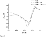
- This phenomenon can be extended for the detection of any type of electromagnetic radiation. If hexaferrite crystal is biased and irradiated by any electromagnetic waves, and/or experiences an internal photoelectric effect, the frequency of ferromagnetic resonance will be changed proportionally to the intensity of absorbed radiation. Therefore, by conducting frequency measurement of the ferromagnetic resonance similar to the approach demonstrated above, it is possible to measure the intensity of the incoming radiation.
- a matrix or array of crystals can be placed in a 2D magnetic field gradient.
- the reference signal can be generated by, for example, a sweep generator with a spectrum broad enough to cover all resonance frequencies of the crystals in the hexaferrite matrix.
- the resonance frequency measurements are made using for example a microwave spectrometer. Since the resonance frequency of each crystal is unique, it is easy to quantify the intensity of electromagnetic radiation which was absorbed by every pixel on the matrix.
- detectors built using this approach can be used for detection of any radiation for example but by no means limited to visible light, ultraviolet light, X-rays and the like. Thus, these detectors can be implemented in a variety of spectrometers and medical imaging modalities.
- an array of MxN hexaferrite resonators as described herein is arranged.
- the matrix size can vary depending on the end application.
- a CT detector matrix will be larger than a digital mammography detector or a fluoroscopy detector.
- the shape of the detector may also vary depending on the potential application - for example, CT detectors would likely be curved but in other applications, the detector may be flat or substantially flat.
- the patient is placed in the external magnetic field B0, and the gradients of the external magnetic field are created along X- and Y-axes (Gx and Gy respectively).
- the patient would be placed between the radiation source and the detector.
- the radiation source and the detector could either rotate around the patient to obtain images at different angles (for CT or fluoroscopy imaging purposes) or remain stationary (for conventional 2D X-ray imaging).
- the radiation attenuated by the patient will be detected by the crystalline array, as discussed above.
- an array of hexaferrite resonators does not require any additional electronic circuits designed for charge collection and/or current measurement. Therefore, manufacturing of the hexaferrite radiation detector described herein will avoid the difficulties associated with solid-state radiation detectors.
- the hexaferrite radiation detector utilizes hexaferrite monocrystals, which significantly improves the charge carrier mobilities.
- the hexaferrite radiation detector has a working frequency of 10-100 GHz which is up to 4 orders of magnitude higher than currently available radiation detectors. Utilization of such operating frequencies produces increases in signal detection speed and will result in significant reduction of radiation dose required for a single scan. In addition, faster performance of the hexaferrite radiation detector will allow for a substantial increase in the resulting image quality.
- the primary advantage of this radiation detection device is the high operating frequencies, as discussed above, which result in a significantly shorter dead time for the detector.
- the known hexaferrite crystal Zn 2 Y experiences ferromagnetic resonance around 12 GHz.
- Barium hexaferrite (BaFe 12 O 19 ) has a resonance frequency - 50 GHz.
- These operating frequencies are several orders of magnitude higher compared to the frequencies commonly used with for example X-ray detection. Therefore, hexaferrite detectors based on photoinduced magnetoelectric effect potentially will have significantly shorter dead-time which means that a lower radiation dose is needed to obtain the same signal-to-noise ratio of an X-ray image.
Landscapes
- Chemical & Material Sciences (AREA)
- Crystallography & Structural Chemistry (AREA)
- Engineering & Computer Science (AREA)
- Power Engineering (AREA)
- Physics & Mathematics (AREA)
- Health & Medical Sciences (AREA)
- Life Sciences & Earth Sciences (AREA)
- General Physics & Mathematics (AREA)
- High Energy & Nuclear Physics (AREA)
- Molecular Biology (AREA)
- Spectroscopy & Molecular Physics (AREA)
- Light Receiving Elements (AREA)
- Crystals, And After-Treatments Of Crystals (AREA)
Claims (6)
- Verfahren zur Bestimmung der Intensität von elektromagnetischer Strahlung, umfassend:Bereitstellung einer Vielzahl von ferrimagnetischen und/oder ferromagnetischen Kristallen, die dazu geeignet sind, einen photoinduzierten magnetoelektrischen Effekt zu erzeugen, angeordnet in einem Array, wobei jeder entsprechende ferrimagnetische oder ferromagnetische Kristall eine unterschiedliche Steuerresonanzfrequenz aufweist;Aussetzung der ferrimagnetischen und/oder ferromagnetischen Kristalle gegenüber elektromagnetischer Strahlung unbekannter oder variabler Intensität, sodass die ferrimagnetischen und/oder ferromagnetischen Kristalle einen internen photoelektrischen Effekt erfahren;Messung einer bestrahlten Resonanzfrequenz der bestrahlten ferrimagnetischen und/oder ferromagnetischen Kristalle; undBestimmung der Intensität der elektromagnetischen Strahlung, die die ferrimagnetischen und/oder ferromagnetischen Kristalle bestrahlt, basierend auf der jeweiligen Steuerresonanzfrequenz und der jeweiligen bestrahlten Resonanzfrequenz.
- Verfahren gemäß Anspruch 1, wobei jeder ferrimagnetische Kristall ein Hexaferrit-Kristall ist.
- Verfahren gemäß Anspruch 1, wobei die Intensität der elektromagnetischen Strahlung proportional zur Änderung der Resonanzfrequenz ist.
- Detektor, umfassend:eine Vielzahl von ferrimagnetischen und/oder ferromagnetischen Kristallen, die zur Erzeugung eines photoinduzierten magnetoelektrischen Effekts geeignet sind, angeordnet in einem Array, wobei sich das Array in einem zweidimensionalen Magnetfeldgradienten (GX, GY) befindet, sodass jeder entsprechende ferrimagnetische und/oder ferromagnetische Kristall eine einzigartige Resonanzfrequenz hat;einen Detektor zur Messung der Intensität einer elektromagnetischen Bestrahlung unterschiedlicher oder unbekannter Intensität; undein Mikrowellen-Spektrometer zur Messung von Resonanzfrequenzen.
- Detektor gemäß Anspruch 4, wobei jeder ferrimagnetische Kristall ein Hexaferrit-Kristall ist.
- Detektor gemäß Anspruch 4, wobei die Intensität der elektromagnetischen Strahlung proportional zur Änderung der Resonanzfrequenz ist.
Applications Claiming Priority (1)
| Application Number | Priority Date | Filing Date | Title |
|---|---|---|---|
| US202163225102P | 2021-07-23 | 2021-07-23 |
Publications (4)
| Publication Number | Publication Date |
|---|---|
| EP4134009A2 EP4134009A2 (de) | 2023-02-15 |
| EP4134009A3 EP4134009A3 (de) | 2023-06-21 |
| EP4134009C0 EP4134009C0 (de) | 2024-11-27 |
| EP4134009B1 true EP4134009B1 (de) | 2024-11-27 |
Family
ID=83271447
Family Applications (1)
| Application Number | Title | Priority Date | Filing Date |
|---|---|---|---|
| EP22185963.0A Active EP4134009B1 (de) | 2021-07-23 | 2022-07-20 | Röntgen- und fotodetektion mit fotoinduziertem magnetoelektrischem effekt |
Country Status (3)
| Country | Link |
|---|---|
| US (1) | US20230028695A1 (de) |
| EP (1) | EP4134009B1 (de) |
| CA (1) | CA3168161A1 (de) |
Family Cites Families (2)
| Publication number | Priority date | Publication date | Assignee | Title |
|---|---|---|---|---|
| US7304309B2 (en) * | 2005-03-14 | 2007-12-04 | Avraham Suhami | Radiation detectors |
| US7358846B2 (en) * | 2005-06-01 | 2008-04-15 | Bernard Doudin | Magnetic spin valve with a magnetoelectric element |
-
2022
- 2022-07-19 US US17/868,001 patent/US20230028695A1/en active Pending
- 2022-07-19 CA CA3168161A patent/CA3168161A1/en active Pending
- 2022-07-20 EP EP22185963.0A patent/EP4134009B1/de active Active
Non-Patent Citations (1)
| Title |
|---|
| JIA QI: "Enhanced Photocurrent in BiFeO 3 Materials by Coupling Temperature and Thermo-Phototronic Effects for Self-Powered Ultraviolet Photodetector System", APPLIED MATERIALS & INTERFACES, vol. 10, no. 16, 25 April 2018 (2018-04-25), US, pages 13712 - 13719, XP093162985, ISSN: 1944-8244, DOI: 10.1021/acsami.8b02543 * |
Also Published As
| Publication number | Publication date |
|---|---|
| EP4134009C0 (de) | 2024-11-27 |
| CA3168161A1 (en) | 2023-01-23 |
| US20230028695A1 (en) | 2023-01-26 |
| EP4134009A3 (de) | 2023-06-21 |
| EP4134009A2 (de) | 2023-02-15 |
Similar Documents
| Publication | Publication Date | Title |
|---|---|---|
| Hou et al. | Materials innovation and electrical engineering in X-ray detection | |
| Duff et al. | Effect of surface preparation technique on the radiation detector performance of CdZnTe | |
| Verger et al. | Characterization of CdTe and CdZnTe detectors for gamma-ray imaging applications | |
| Hu et al. | Ultrafast inorganic scintillator-based front imager for Gigahertz Hard X-ray imaging | |
| CN103261914B (zh) | 直接转换x射线探测器 | |
| Sarkar et al. | Defect driven ferromagnetism in SnO 2: a combined study using density functional theory and positron annihilation spectroscopy | |
| Abbene et al. | Development of new CdZnTe detectors for room-temperature high-flux radiation measurements | |
| US9958556B1 (en) | Direct conversion radiation detector | |
| JP2016202901A (ja) | 検出器装置及びx線ct装置 | |
| Iizawa et al. | Energy-resolved neutron imaging with high spatial resolution using a superconducting delay-line kinetic inductance detector | |
| US10338237B2 (en) | Inductive radiation detector | |
| Carpenter et al. | Development of Ta-based superconducting tunnel junction X-ray detector arrays | |
| Nocente et al. | Experimental investigation of silicon photomultipliers as compact light readout systems for gamma-ray spectroscopy applications in fusion plasmas | |
| EP4134009A2 (de) | Röntgen- und fotodetektion mit fotoinduziertem magnetoelektrischem effekt | |
| Burger et al. | Development of portable CdZnTe spectrometers for remote sensing of signatures from nuclear materials | |
| Tan et al. | Phase diagram and neutron spin resonance of superconducting NaFe 1− x Cu x As | |
| Risticj | The digital flat-panel x-ray detectors | |
| Fan et al. | Development of a fast electron bremsstrahlung diagnostic system based on LYSO and silicon photomultipliers during lower hybrid current drive for tokamak | |
| Hirayama et al. | Interchannel crosstalk and nonlinearity of microwave SQUID multiplexers | |
| Song et al. | Significant sensitivity enhancement of single crystal CdSe x-ray detector by liquid nitrogen cooling | |
| Rosenberg et al. | Elemental and magnetic sensitive imaging using x-ray excited luminescence microscopy | |
| Vu et al. | Narrow-area Bragg-edge transmission of iron samples using superconducting neutron sensor | |
| Camlica et al. | Increased temporal resolution of amorphous selenium detector using preferential charge sensing approach | |
| Lee et al. | Study of silicon photodiode performance for X-ray detector in cargo system | |
| Giakos | A slot-scanned detector operating on gas-solid state imaging principles |
Legal Events
| Date | Code | Title | Description |
|---|---|---|---|
| PUAI | Public reference made under article 153(3) epc to a published international application that has entered the european phase |
Free format text: ORIGINAL CODE: 0009012 |
|
| STAA | Information on the status of an ep patent application or granted ep patent |
Free format text: STATUS: THE APPLICATION HAS BEEN PUBLISHED |
|
| AK | Designated contracting states |
Kind code of ref document: A2 Designated state(s): AL AT BE BG CH CY CZ DE DK EE ES FI FR GB GR HR HU IE IS IT LI LT LU LV MC MK MT NL NO PL PT RO RS SE SI SK SM TR |
|
| PUAL | Search report despatched |
Free format text: ORIGINAL CODE: 0009013 |
|
| AK | Designated contracting states |
Kind code of ref document: A3 Designated state(s): AL AT BE BG CH CY CZ DE DK EE ES FI FR GB GR HR HU IE IS IT LI LT LU LV MC MK MT NL NO PL PT RO RS SE SI SK SM TR |
|
| RIC1 | Information provided on ipc code assigned before grant |
Ipc: G01R 29/08 20060101ALI20230512BHEP Ipc: H10N 35/85 20230101ALI20230512BHEP Ipc: H10N 30/85 20230101ALI20230512BHEP Ipc: G01J 1/42 20060101ALI20230512BHEP Ipc: A61B 6/03 20060101AFI20230512BHEP |
|
| STAA | Information on the status of an ep patent application or granted ep patent |
Free format text: STATUS: REQUEST FOR EXAMINATION WAS MADE |
|
| 17P | Request for examination filed |
Effective date: 20231220 |
|
| RBV | Designated contracting states (corrected) |
Designated state(s): AL AT BE BG CH CY CZ DE DK EE ES FI FR GB GR HR HU IE IS IT LI LT LU LV MC MK MT NL NO PL PT RO RS SE SI SK SM TR |
|
| REG | Reference to a national code |
Ref country code: DE Ref legal event code: R079 Free format text: PREVIOUS MAIN CLASS: A61B0006030000 Ipc: H10N0035850000 Ref document number: 602022008109 Country of ref document: DE |
|
| RIC1 | Information provided on ipc code assigned before grant |
Ipc: G01T 1/24 20060101ALI20240516BHEP Ipc: H10N 35/85 20230101AFI20240516BHEP |
|
| GRAP | Despatch of communication of intention to grant a patent |
Free format text: ORIGINAL CODE: EPIDOSNIGR1 |
|
| STAA | Information on the status of an ep patent application or granted ep patent |
Free format text: STATUS: GRANT OF PATENT IS INTENDED |
|
| INTG | Intention to grant announced |
Effective date: 20240624 |
|
| GRAS | Grant fee paid |
Free format text: ORIGINAL CODE: EPIDOSNIGR3 |
|
| GRAA | (expected) grant |
Free format text: ORIGINAL CODE: 0009210 |
|
| STAA | Information on the status of an ep patent application or granted ep patent |
Free format text: STATUS: THE PATENT HAS BEEN GRANTED |
|
| AK | Designated contracting states |
Kind code of ref document: B1 Designated state(s): AL AT BE BG CH CY CZ DE DK EE ES FI FR GB GR HR HU IE IS IT LI LT LU LV MC MK MT NL NO PL PT RO RS SE SI SK SM TR |
|
| REG | Reference to a national code |
Ref country code: GB Ref legal event code: FG4D |
|
| REG | Reference to a national code |
Ref country code: CH Ref legal event code: EP |
|
| REG | Reference to a national code |
Ref country code: IE Ref legal event code: FG4D |
|
| REG | Reference to a national code |
Ref country code: DE Ref legal event code: R096 Ref document number: 602022008109 Country of ref document: DE |
|
| U01 | Request for unitary effect filed |
Effective date: 20241219 |
|
| U07 | Unitary effect registered |
Designated state(s): AT BE BG DE DK EE FI FR IT LT LU LV MT NL PT RO SE SI Effective date: 20250114 |
|
| PG25 | Lapsed in a contracting state [announced via postgrant information from national office to epo] |
Ref country code: HR Free format text: LAPSE BECAUSE OF FAILURE TO SUBMIT A TRANSLATION OF THE DESCRIPTION OR TO PAY THE FEE WITHIN THE PRESCRIBED TIME-LIMIT Effective date: 20241127 Ref country code: IS Free format text: LAPSE BECAUSE OF FAILURE TO SUBMIT A TRANSLATION OF THE DESCRIPTION OR TO PAY THE FEE WITHIN THE PRESCRIBED TIME-LIMIT Effective date: 20250327 |
|
| PG25 | Lapsed in a contracting state [announced via postgrant information from national office to epo] |
Ref country code: ES Free format text: LAPSE BECAUSE OF FAILURE TO SUBMIT A TRANSLATION OF THE DESCRIPTION OR TO PAY THE FEE WITHIN THE PRESCRIBED TIME-LIMIT Effective date: 20241127 |
|
| PG25 | Lapsed in a contracting state [announced via postgrant information from national office to epo] |
Ref country code: NO Free format text: LAPSE BECAUSE OF FAILURE TO SUBMIT A TRANSLATION OF THE DESCRIPTION OR TO PAY THE FEE WITHIN THE PRESCRIBED TIME-LIMIT Effective date: 20250227 |
|
| PG25 | Lapsed in a contracting state [announced via postgrant information from national office to epo] |
Ref country code: GR Free format text: LAPSE BECAUSE OF FAILURE TO SUBMIT A TRANSLATION OF THE DESCRIPTION OR TO PAY THE FEE WITHIN THE PRESCRIBED TIME-LIMIT Effective date: 20250228 |
|
| PG25 | Lapsed in a contracting state [announced via postgrant information from national office to epo] |
Ref country code: PL Free format text: LAPSE BECAUSE OF FAILURE TO SUBMIT A TRANSLATION OF THE DESCRIPTION OR TO PAY THE FEE WITHIN THE PRESCRIBED TIME-LIMIT Effective date: 20241127 |
|
| PG25 | Lapsed in a contracting state [announced via postgrant information from national office to epo] |
Ref country code: RS Free format text: LAPSE BECAUSE OF FAILURE TO SUBMIT A TRANSLATION OF THE DESCRIPTION OR TO PAY THE FEE WITHIN THE PRESCRIBED TIME-LIMIT Effective date: 20250227 |
|
| PG25 | Lapsed in a contracting state [announced via postgrant information from national office to epo] |
Ref country code: SM Free format text: LAPSE BECAUSE OF FAILURE TO SUBMIT A TRANSLATION OF THE DESCRIPTION OR TO PAY THE FEE WITHIN THE PRESCRIBED TIME-LIMIT Effective date: 20241127 |
|
| PG25 | Lapsed in a contracting state [announced via postgrant information from national office to epo] |
Ref country code: SK Free format text: LAPSE BECAUSE OF FAILURE TO SUBMIT A TRANSLATION OF THE DESCRIPTION OR TO PAY THE FEE WITHIN THE PRESCRIBED TIME-LIMIT Effective date: 20241127 |
|
| PG25 | Lapsed in a contracting state [announced via postgrant information from national office to epo] |
Ref country code: CZ Free format text: LAPSE BECAUSE OF FAILURE TO SUBMIT A TRANSLATION OF THE DESCRIPTION OR TO PAY THE FEE WITHIN THE PRESCRIBED TIME-LIMIT Effective date: 20241127 |
|
| U20 | Renewal fee for the european patent with unitary effect paid |
Year of fee payment: 4 Effective date: 20250728 |
|
| PLBE | No opposition filed within time limit |
Free format text: ORIGINAL CODE: 0009261 |
|
| STAA | Information on the status of an ep patent application or granted ep patent |
Free format text: STATUS: NO OPPOSITION FILED WITHIN TIME LIMIT |
|
| REG | Reference to a national code |
Ref country code: CH Ref legal event code: L10 Free format text: ST27 STATUS EVENT CODE: U-0-0-L10-L00 (AS PROVIDED BY THE NATIONAL OFFICE) Effective date: 20251008 |
|
| 26N | No opposition filed |
Effective date: 20250828 |
|
| REG | Reference to a national code |
Ref country code: CH Ref legal event code: H13 Free format text: ST27 STATUS EVENT CODE: U-0-0-H10-H13 (AS PROVIDED BY THE NATIONAL OFFICE) Effective date: 20260224 |
|
| PG25 | Lapsed in a contracting state [announced via postgrant information from national office to epo] |
Ref country code: CH Free format text: LAPSE BECAUSE OF NON-PAYMENT OF DUE FEES Effective date: 20250731 |