EP4131714A2 - Leistungswandlerschaltung sowie ladegerät und system - Google Patents
Leistungswandlerschaltung sowie ladegerät und system Download PDFInfo
- Publication number
- EP4131714A2 EP4131714A2 EP22176915.1A EP22176915A EP4131714A2 EP 4131714 A2 EP4131714 A2 EP 4131714A2 EP 22176915 A EP22176915 A EP 22176915A EP 4131714 A2 EP4131714 A2 EP 4131714A2
- Authority
- EP
- European Patent Office
- Prior art keywords
- switch element
- battery
- power conversion
- conversion circuit
- charging
- Prior art date
- Legal status (The legal status is an assumption and is not a legal conclusion. Google has not performed a legal analysis and makes no representation as to the accuracy of the status listed.)
- Pending
Links
Images





Classifications
-
- H—ELECTRICITY
- H02—GENERATION; CONVERSION OR DISTRIBUTION OF ELECTRIC POWER
- H02J—ELECTRIC POWER NETWORKS; CIRCUIT ARRANGEMENTS OR SYSTEMS FOR SUPPLYING OR DISTRIBUTING ELECTRIC POWER; SYSTEMS FOR STORING ELECTRIC ENERGY
- H02J7/00—Circuit arrangements for charging or discharging batteries or for supplying loads from batteries
- H02J7/90—Regulation of charging or discharging current or voltage
-
- G—PHYSICS
- G06—COMPUTING OR CALCULATING; COUNTING
- G06F—ELECTRIC DIGITAL DATA PROCESSING
- G06F1/00—Details not covered by groups G06F3/00 - G06F13/00 and G06F21/00
- G06F1/26—Power supply means, e.g. regulation thereof
- G06F1/263—Arrangements for using multiple switchable power supplies, e.g. battery and AC
-
- H—ELECTRICITY
- H02—GENERATION; CONVERSION OR DISTRIBUTION OF ELECTRIC POWER
- H02J—ELECTRIC POWER NETWORKS; CIRCUIT ARRANGEMENTS OR SYSTEMS FOR SUPPLYING OR DISTRIBUTING ELECTRIC POWER; SYSTEMS FOR STORING ELECTRIC ENERGY
- H02J7/00—Circuit arrangements for charging or discharging batteries or for supplying loads from batteries
-
- H—ELECTRICITY
- H02—GENERATION; CONVERSION OR DISTRIBUTION OF ELECTRIC POWER
- H02J—ELECTRIC POWER NETWORKS; CIRCUIT ARRANGEMENTS OR SYSTEMS FOR SUPPLYING OR DISTRIBUTING ELECTRIC POWER; SYSTEMS FOR STORING ELECTRIC ENERGY
- H02J7/00—Circuit arrangements for charging or discharging batteries or for supplying loads from batteries
- H02J7/40—Circuit arrangements for charging or discharging batteries or for supplying loads from batteries characterised by the exchange of charge or discharge related data
- H02J7/42—Circuit arrangements for charging or discharging batteries or for supplying loads from batteries characterised by the exchange of charge or discharge related data with electronic devices having internal batteries, e.g. mobile phones
-
- H—ELECTRICITY
- H02—GENERATION; CONVERSION OR DISTRIBUTION OF ELECTRIC POWER
- H02J—ELECTRIC POWER NETWORKS; CIRCUIT ARRANGEMENTS OR SYSTEMS FOR SUPPLYING OR DISTRIBUTING ELECTRIC POWER; SYSTEMS FOR STORING ELECTRIC ENERGY
- H02J7/00—Circuit arrangements for charging or discharging batteries or for supplying loads from batteries
- H02J7/40—Circuit arrangements for charging or discharging batteries or for supplying loads from batteries characterised by the exchange of charge or discharge related data
- H02J7/44—Circuit arrangements for charging or discharging batteries or for supplying loads from batteries characterised by the exchange of charge or discharge related data between battery management systems and power sources
-
- H—ELECTRICITY
- H02—GENERATION; CONVERSION OR DISTRIBUTION OF ELECTRIC POWER
- H02J—ELECTRIC POWER NETWORKS; CIRCUIT ARRANGEMENTS OR SYSTEMS FOR SUPPLYING OR DISTRIBUTING ELECTRIC POWER; SYSTEMS FOR STORING ELECTRIC ENERGY
- H02J7/00—Circuit arrangements for charging or discharging batteries or for supplying loads from batteries
- H02J7/40—Circuit arrangements for charging or discharging batteries or for supplying loads from batteries characterised by the exchange of charge or discharge related data
- H02J7/47—Arrangements for checking compatibility or authentication between one component, e.g. a battery or a battery charger, and another component, e.g. a power source
-
- H—ELECTRICITY
- H02—GENERATION; CONVERSION OR DISTRIBUTION OF ELECTRIC POWER
- H02J—ELECTRIC POWER NETWORKS; CIRCUIT ARRANGEMENTS OR SYSTEMS FOR SUPPLYING OR DISTRIBUTING ELECTRIC POWER; SYSTEMS FOR STORING ELECTRIC ENERGY
- H02J7/00—Circuit arrangements for charging or discharging batteries or for supplying loads from batteries
- H02J7/50—Circuit arrangements for charging or discharging batteries or for supplying loads from batteries acting upon multiple batteries simultaneously or sequentially
-
- H—ELECTRICITY
- H02—GENERATION; CONVERSION OR DISTRIBUTION OF ELECTRIC POWER
- H02M—APPARATUS FOR CONVERSION BETWEEN AC AND AC, BETWEEN AC AND DC, OR BETWEEN DC AND DC, AND FOR USE WITH MAINS OR SIMILAR POWER SUPPLY SYSTEMS; CONVERSION OF DC OR AC INPUT POWER INTO SURGE OUTPUT POWER; CONTROL OR REGULATION THEREOF
- H02M3/00—Conversion of DC power input into DC power output
- H02M3/02—Conversion of DC power input into DC power output without intermediate conversion into AC
- H02M3/04—Conversion of DC power input into DC power output without intermediate conversion into AC by static converters
- H02M3/10—Conversion of DC power input into DC power output without intermediate conversion into AC by static converters using discharge tubes with control electrode or semiconductor devices with control electrode
- H02M3/145—Conversion of DC power input into DC power output without intermediate conversion into AC by static converters using discharge tubes with control electrode or semiconductor devices with control electrode using devices of a triode or transistor type requiring continuous application of a control signal
- H02M3/155—Conversion of DC power input into DC power output without intermediate conversion into AC by static converters using discharge tubes with control electrode or semiconductor devices with control electrode using devices of a triode or transistor type requiring continuous application of a control signal using semiconductor devices only
- H02M3/156—Conversion of DC power input into DC power output without intermediate conversion into AC by static converters using discharge tubes with control electrode or semiconductor devices with control electrode using devices of a triode or transistor type requiring continuous application of a control signal using semiconductor devices only with automatic control of output voltage or current, e.g. switching regulators
- H02M3/158—Conversion of DC power input into DC power output without intermediate conversion into AC by static converters using discharge tubes with control electrode or semiconductor devices with control electrode using devices of a triode or transistor type requiring continuous application of a control signal using semiconductor devices only with automatic control of output voltage or current, e.g. switching regulators including plural semiconductor devices as final control devices for a single load
-
- H—ELECTRICITY
- H02—GENERATION; CONVERSION OR DISTRIBUTION OF ELECTRIC POWER
- H02M—APPARATUS FOR CONVERSION BETWEEN AC AND AC, BETWEEN AC AND DC, OR BETWEEN DC AND DC, AND FOR USE WITH MAINS OR SIMILAR POWER SUPPLY SYSTEMS; CONVERSION OF DC OR AC INPUT POWER INTO SURGE OUTPUT POWER; CONTROL OR REGULATION THEREOF
- H02M7/00—Conversion of AC power input into DC power output; Conversion of DC power input into AC power output
- H02M7/42—Conversion of DC power input into AC power output without possibility of reversal
- H02M7/44—Conversion of DC power input into AC power output without possibility of reversal by static converters
- H02M7/48—Conversion of DC power input into AC power output without possibility of reversal by static converters using discharge tubes with control electrode or semiconductor devices with control electrode
- H02M7/483—Converters with outputs that each can have more than two voltages levels
- H02M7/4837—Flying capacitor converters
-
- H—ELECTRICITY
- H02—GENERATION; CONVERSION OR DISTRIBUTION OF ELECTRIC POWER
- H02J—ELECTRIC POWER NETWORKS; CIRCUIT ARRANGEMENTS OR SYSTEMS FOR SUPPLYING OR DISTRIBUTING ELECTRIC POWER; SYSTEMS FOR STORING ELECTRIC ENERGY
- H02J2207/00—Details of circuit arrangements for charging or discharging batteries or supplying loads from batteries
- H02J2207/20—Charging or discharging characterised by the power electronics converter
-
- H—ELECTRICITY
- H02—GENERATION; CONVERSION OR DISTRIBUTION OF ELECTRIC POWER
- H02J—ELECTRIC POWER NETWORKS; CIRCUIT ARRANGEMENTS OR SYSTEMS FOR SUPPLYING OR DISTRIBUTING ELECTRIC POWER; SYSTEMS FOR STORING ELECTRIC ENERGY
- H02J2207/00—Details of circuit arrangements for charging or discharging batteries or supplying loads from batteries
- H02J2207/30—Charge provided using DC bus or data bus of a computer
-
- H—ELECTRICITY
- H02—GENERATION; CONVERSION OR DISTRIBUTION OF ELECTRIC POWER
- H02M—APPARATUS FOR CONVERSION BETWEEN AC AND AC, BETWEEN AC AND DC, OR BETWEEN DC AND DC, AND FOR USE WITH MAINS OR SIMILAR POWER SUPPLY SYSTEMS; CONVERSION OF DC OR AC INPUT POWER INTO SURGE OUTPUT POWER; CONTROL OR REGULATION THEREOF
- H02M1/00—Details of apparatus for conversion
- H02M1/0095—Hybrid converter topologies, e.g. NPC mixed with flying capacitor, thyristor converter mixed with MMC or charge pump mixed with buck
-
- H—ELECTRICITY
- H02—GENERATION; CONVERSION OR DISTRIBUTION OF ELECTRIC POWER
- H02M—APPARATUS FOR CONVERSION BETWEEN AC AND AC, BETWEEN AC AND DC, OR BETWEEN DC AND DC, AND FOR USE WITH MAINS OR SIMILAR POWER SUPPLY SYSTEMS; CONVERSION OF DC OR AC INPUT POWER INTO SURGE OUTPUT POWER; CONTROL OR REGULATION THEREOF
- H02M3/00—Conversion of DC power input into DC power output
- H02M3/02—Conversion of DC power input into DC power output without intermediate conversion into AC
- H02M3/04—Conversion of DC power input into DC power output without intermediate conversion into AC by static converters
- H02M3/06—Conversion of DC power input into DC power output without intermediate conversion into AC by static converters using resistors or capacitors, e.g. potential divider
- H02M3/07—Conversion of DC power input into DC power output without intermediate conversion into AC by static converters using resistors or capacitors, e.g. potential divider using capacitors charged and discharged alternately by semiconductor devices with control electrode, e.g. charge pumps
Definitions
- This application relates to the field of circuits, and more specifically, to a power conversion circuit, and a charging apparatus and system.
- a battery provides energy, in a form of a voltage or a current, that allows a circuit to operate.
- energy stored in a battery is limited, and when an electronic apparatus is in use, the battery loses electric power.
- a voltage of the battery starts to decrease from a rated voltage of the battery, and the electronic apparatus that obtains electric power depending on the battery is not suitable for continuing operating.
- a battery charging system in a specific form is required.
- a battery charging system includes a power adapter and a charging apparatus. Energy and information are usually transferred between the power adapter and the charging apparatus through a USB cable.
- a purpose of the power adapter is to transfer energy of a utility power supply to the charging apparatus in a specific voltage manner.
- a purpose of the charging apparatus is to perform voltage transformation on energy obtained by using the power adapter and then transfer energy to the battery.
- an existing battery charging system supports only one voltage mode.
- different batteries support different quantities of electricity, voltages, and currents.
- the battery When charging is limited, if an excessively large voltage or current is supplied to a battery, the battery may be damaged or even explode; or if an excessively small voltage or current is supplied to a battery, a charging process may be inefficient or completely ineffective.
- This application provides a power conversion circuit, and a charging apparatus and system, to support a plurality of charging modes and effectively increase a battery charging rate.
- a power conversion circuit includes: a first switch element, a second switch element, a third switch element, a fourth switch element, a fifth switch element, a sixth switch element, a first energy storage element, and a second energy storage element.
- a first end of the first switch element is coupled and connected to an input power supply through a first external connection end of the power conversion circuit; a second end of the first switch element is separately coupled to a first end of the first energy storage element, a first end of the second switch element, and a first end of the fifth switch element; a second end of the first energy storage element is separately coupled to a first end of the third switch element, a first end of the fourth switch element, and a first end of the sixth switch element; a second end of the second switch element is coupled and connected to a battery through a second external connection end of the power conversion circuit; a second end of the fifth switch element is separately coupled to a first end of the second energy storage element and a second end of the sixth switch element; a second end of the second energy storage element is coupled to the second external connection end; a second end of the fourth switch element is coupled to the second external connection end; and a second end of the third switch element is grounded.
- the power conversion circuit further includes a seventh switch element, where a first end of the seventh switch element is separately coupled to the second end of the first switch element, the first end of the second switch element, the first end of the fifth switch element, and the first end of the first energy storage element; and a second end of the seventh switch element is separately coupled to the first end of the third switch element, the first end of the fourth switch element, the first end of the sixth switch element, and the second end of the first energy storage element.
- a charging apparatus includes the power conversion circuit in the foregoing aspect and implementation, an input/output port, and an information collection and signal control circuit coupled to the power conversion circuit, and the information collection and signal control circuit is coupled and connected to the input/output port.
- the information collection and signal control circuit includes: a digital core processing element, a battery information detection element, an output drive element, an information input element, a first power conversion element, and a second power conversion element.
- the information input element, the first power conversion element, and the second power conversion element are separately coupled and connected to the input power supply through a first external connection end of the information collection and signal control circuit;
- the information input element is connected to the digital core processing element;
- the first power conversion element is connected to the digital core processing element;
- the second power conversion element is connected to the output drive element;
- the digital core processing element is coupled and connected to a data line of a power adapter through a second external connection end of the information collection and signal control circuit;
- the digital core processing element is connected to the battery information detection element;
- the battery information detection element is coupled and connected to a battery through a third external connection end of the information collection and signal control circuit;
- the digital core processing element is connected to the output drive element; and the output drive element is separately coupled to each switch element in
- a first end of the input/output port is connected to the input power supply of the power adapter, a second end of the input/output port is separately coupled to the first external connection end of the power conversion circuit and the first external connection end of the information collection and signal control circuit, a third end of the input/output port is connected to the data line of the power adapter, and a fourth end of the input/output port is coupled to the second external connection end of the information collection and signal control circuit.
- the input/output port is a USB port.
- a charging system includes the charging apparatus in the foregoing aspect and implementations, and a power adapter and a battery element that are coupled to the charging apparatus.
- the charging apparatus and the battery element may be disposed in one device, and the device may be a terminal, a base station, or an electric vehicle.
- a method for charging a battery by a power conversion circuit is provided.
- the power conversion circuit may charge the battery based on a first charging mode, and the method includes: keeping the second switch element and the sixth switch element open, and keeping the fifth switch element closed, where in a first time period, the first switch element and the fourth switch element are in a closed state, the third switch element is in an open state, and the first energy storage element and the second energy storage element are charged; and in a second time period after the first time period, the first switch element and the fourth switch element are in an open state, the third switch element is in a closed state, and the first energy storage element and the second energy storage element are discharged.
- the power conversion circuit may charge the battery based on a second charging mode
- the method includes: keeping the fourth switch element and the fifth switch element open, and keeping the sixth switch element closed, where in a first time period, the first switch element is in a closed state, the second switch element and the third switch element are in an open state, and the first energy storage element and the second energy storage element are charged; and in a second time period after the first time period, the first switch element is in an open state, the second switch element and the third switch element are in a closed state, and the first energy storage element and the second energy storage element are discharged.
- the power conversion circuit may charge the battery based on a third charging mode, and the method includes: keeping the fifth switch element and the sixth switch element open, where in a first time period, the first switch element and the fourth switch element are in a closed state, the second switch element and the third switch element are in an open state, and the first energy storage element is charged; and in a second time period after the first time period, the first switch element and the fourth switch element are in an open state, the second switch element and the third switch element are in a closed state, and the first energy storage element is discharged.
- the power conversion circuit may charge the battery based on a fourth charging mode, and the method includes: keeping the fourth switch element, the fifth switch element, and the sixth switch element open, and keeping the first switch element and the third switch element closed, where in a first time period, the second switch element is in a closed state, and the battery is directly charged; and in a second time period after the first time period, the second switch element is in an open state, and battery charging is suspended.
- the power conversion circuit may charge the battery based on a fifth charging mode
- the method includes: keeping the second switch element, the fourth switch element, and the sixth switch element open, and keeping the fifth switch element and the seventh switch element closed, where in a first time period, the first switch element is in a closed state, the third switch element is in an open state, and the second energy storage element is charged; and in a second time period after the first time period, the first switch element is in an open state, the third switch element is in a closed state, and the second energy storage element is discharged.
- the power conversion circuit may charge the battery based on a sixth charging mode, and the method includes: keeping the second switch element, the fourth switch element, and the fifth switch element open, and keeping the sixth switch element and the seventh switch element closed, where in a first time period, the first switch element is in a closed state, the third switch element is in an open state, and the second energy storage element is charged; and in a second time period after the first time period, the first switch element is in an open state, the third switch element is in a closed state, and the second energy storage element is discharged.
- the power conversion circuit includes: a first switch element, a second switch element, a third switch element, a seventh switch element, a first energy storage element, and a second energy storage element.
- a first end of the first switch element is coupled and connected to an input power supply through a first external connection end of the power conversion circuit;
- a second end of the first switch element is separately coupled to a first end of the second switch element, a first end of the seventh switch element, and a first end of the first energy storage element;
- a second end of the first energy storage element is separately coupled to a first end of the second energy storage element, a first end of the third switch element, and a second end of the seventh switch element;
- a second end of the second switch element is coupled and connected to a battery through a second external connection end of the power conversion circuit;
- a second end of the second energy storage element is coupled to the second external connection end; and
- a second end of the third switch element is grounded.
- the power conversion circuit may charge the battery based on a second charging mode or a sixth charging mode.
- the power conversion circuit includes: a first switch element, a second switch element, a third switch element, a fifth switch element, a seventh switch element, a first energy storage element, and a second energy storage element.
- a first end of the first switch element is coupled and connected to an input power supply through a first external connection end of the power conversion circuit; a second end of the first switch element is separately coupled to a first end of the second switch element, a first end of the fifth switch element, a first end of the seventh switch element, and a first end of the first energy storage element; a second end of the first energy storage element is separately coupled to a first end of the third switch element and a second end of the seventh switch element; a second end of the second switch element is coupled and connected to a battery through a second external connection end of the power conversion circuit; a second end of the fifth switch element is connected to a first end of the second energy storage element; a second end of the second energy storage element is coupled to the second external connection end; and a second end of the third switch element is grounded.
- the power conversion circuit may charge the battery based on a second charging mode, a fourth charging mode, a fifth charging mode, or a sixth charging mode.
- the power conversion circuit further includes a fourth switch element, where a first end of the fourth switch element is separately coupled to the first end of the third switch element, the second end of the seventh switch element, and the second end of the first energy storage element; and a second end of the fourth switch element is coupled to the second external connection end.
- the power conversion circuit may alternatively charge the battery based on a third charging mode.
- the power conversion circuit includes: a first switch element, a second switch element, a third switch element, a sixth switch element, a seventh switch element, a first energy storage element, and a second energy storage element.
- a first end of the first switch element is coupled and connected to an input power supply through a first external connection end of the power conversion circuit; a second end of the first switch element is separately coupled to a first end of the second switch element, a first end of the seventh switch element, and a first end of the first energy storage element; a second end of the first energy storage element is separately coupled to a first end of the third switch element, a first end of the sixth switch element, and a second end of the seventh switch element; a second end of the second switch element is coupled and connected to a battery through a second external connection end of the power conversion circuit; a second end of the sixth switch element is connected to a first end of the second energy storage element; a second end of the second energy storage element is coupled to the second external connection end; and a second end of the third switch element is grounded.
- the power conversion circuit may charge the battery based on a second charging mode, a fourth charging mode, or a sixth charging mode.
- the power conversion circuit further includes a fourth switch element, where a first end of the fourth switch element is separately coupled to the first end of the third switch element, the first end of the sixth switch element, the second end of the seventh switch element, and the second end of the first energy storage element; and a second end of the fourth switch element is coupled to the second external connection end.
- the power conversion circuit may alternatively charge the battery based on a third charging mode.
- the power conversion circuit includes: a first switch element, a second switch element, a third switch element, a fourth switch element, and a first energy storage element.
- a first end of the first switch element is coupled and connected to an input power supply through a first external connection end of the power conversion circuit
- a second end of the first switch element is separately coupled to a first end of the second switch element and a first end of the first energy storage element
- a second end of the first energy storage element is separately coupled to a first end of the third switch element and a first end of the fourth switch element
- a second end of the second switch element is coupled and connected to a battery through a second external connection end of the power conversion circuit
- a second end of the fourth switch element is coupled to the second external connection end
- a second end of the third switch element is grounded.
- the power conversion circuit may charge the battery based on a third charging mode or a fourth charging mode.
- the power conversion circuit further includes a fifth switch element and a second energy storage element, where a first end of the fifth switch element is separately coupled to the second end of the first switch element, the first end of the second switch element, and the first end of the first energy storage element; a second end of the fifth switch element is connected to a first end of the second energy storage element; and a second end of the second energy storage element is coupled to the second external connection end.
- the power conversion circuit may alternatively charge the battery based on a first charging mode.
- the power conversion circuit includes: a first switch element, a second switch element, a third switch element, a sixth switch element, a first energy storage element, and a second energy storage element.
- a first end of the first switch element is coupled and connected to an input power supply through a first external connection end of the power conversion circuit
- a second end of the first switch element is separately coupled to a first end of the second switch element and a first end of the first energy storage element
- a second end of the first energy storage element is separately coupled to a first end of the third switch element and a first end of the sixth switch element
- a second end of the second switch element is coupled and connected to a battery through a second external connection end of the power conversion circuit
- a second end of the sixth switch element is connected to a first end of the second energy storage element
- a second end of the second energy storage element is coupled to the second external connection end
- a second end of the third switch element is grounded.
- the power conversion circuit may charge the battery based on a second charging mode or a fourth charging mode.
- the power conversion circuit further includes a fourth switch element, where a first end of the fourth switch element is separately coupled to the first end of the third switch element, the first end of the sixth switch element, and the second end of the first energy storage element; and a second end of the fourth switch element is coupled to the second external connection end.
- the power conversion circuit may alternatively charge the battery based on a third charging mode.
- the power conversion circuit includes: a first switch element, a third switch element, a fourth switch element, a seventh switch element, a first energy storage element, and a second energy storage element.
- a first end of the first switch element is coupled and connected to an input power supply through a first external connection end of the power conversion circuit;
- a second end of the first switch element is separately coupled to a first end of the seventh switch element, a first end of the first energy storage element, and a first end of the second energy storage element;
- a second end of the first energy storage element is separately coupled to a first end of the third switch element, a first end of the fourth switch element, and a second end of the seventh switch element;
- a second end of the second energy storage element is coupled and connected to a battery through a second external connection end of the power conversion circuit;
- a second end of the fourth switch element is coupled to the second external connection end; and a second end of the third switch element is grounded.
- the power conversion circuit may charge the battery based on a first charging mode or a fifth charging mode.
- the power conversion circuit includes: a first switch element, a third switch element, a fourth switch element, a fifth switch element, a sixth switch element, a seventh switch element, a first energy storage element, and a second energy storage element.
- a first end of the first switch element is coupled and connected to an input power supply through a first external connection end of the power conversion circuit; a second end of the first switch element is separately coupled to a first end of the fifth switch element, a first end of the seventh switch element, and a first end of the first energy storage element; a second end of the first energy storage element is separately coupled to a first end of the third switch element, a first end of the fourth switch element, a first end of the sixth switch element, and a second end of the seventh switch element; a first end of the second energy storage element is separately coupled to a second end of the fifth switch element and a second end of the sixth switch element; a second end of the second energy storage element is coupled and connected to a battery through a second external connection end of the power conversion circuit; a second end of the fourth switch element is coupled to the second external connection end; and a second end of the third switch element is grounded.
- the power conversion circuit may charge the battery based on a first charging mode, a fifth charging mode, or a sixth charging mode.
- a plurality of different charging modes can be supported. This can not only meet a battery charging requirement, but also effectively increase a battery charging rate.
- the first energy storage element is a capacitor
- the second energy storage element is an inductor
- the first energy storage element includes at least two capacitors that are connected in parallel
- the second energy storage element includes at least two inductors that are connected in series.
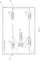
- FIG. 1 shows a charging apparatus 100 according to an embodiment of the present invention.
- the charging apparatus 100 may be configured to convert input power energy based on a preset mode and then provide energy for a battery.
- the charging apparatus 100 includes a power conversion circuit 101, an information collection and signal control circuit 102, and an input/output port 103.
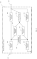
- FIG. 2 shows a structure of the power conversion circuit according to an embodiment of the present invention.
- the power conversion circuit 101 is configured to convert a power supply V BUS into power energy required by a battery.
- the power conversion circuit 101 includes: a first switch element 201, a second switch element 202, a third switch element 203, a fourth switch element 204, a fifth switch element 205, a sixth switch element 206, a first energy storage element 207, and a second energy storage element 208.
- a first end of the first switch element 201 is coupled and connected to the power supply V BUS through a first external connection end 209 of the power conversion circuit 101; a second end of the first switch element 201 is separately coupled to a first end of the first energy storage element 207, a first end of the second switch element 202, and a first end of the fifth switch element 205; a second end of the first energy storage element 207 is separately coupled to a first end of the third switch element 203, a first end of the fourth switch element 204, and a first end of the sixth switch element 206; a second end of the second switch element 202 is coupled and connected to a battery through a second external connection end 210 of the power conversion circuit 101; a second end of the fifth switch element 205 is separately coupled to a first end of the second energy storage element 208 and a second end of the sixth switch element 206; a second end of the second energy storage element 208 is coupled to the second external connection end 210; a second end of the fourth
- the first energy storage element 207 and the second energy storage element 208 each may be one or more devices that can store energy and can release the stored energy.
- the device is a capacitor or an inductor.
- the first energy storage element 207 and the second energy storage element 208 may have different device types.
- the first energy storage element 207 is a capacitor
- the second energy storage element 208 is an inductor.
- the first energy storage element 207 includes at least two capacitors that are connected in parallel
- the second energy storage element 208 includes at least two inductors that are connected in series.
- a device type, a device quantity, and a device composition form that are included in an energy storage element are not limited in this embodiment of the present invention.
- At least one of the first switch element 201, the second switch element 202, the third switch element 203, the fourth switch element 204, the fifth switch element 205, and the sixth switch element 206 is a metal oxide semiconductor (metal oxide semiconductor, MOS) field effect transistor or a bipolar junction transistor (bipolar junction transistor, BJT). This is not limited in the embodiments of the present invention.
- MOS metal oxide semiconductor
- BJT bipolar junction transistor
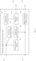
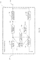
- FIG. 3 shows a structure of the information collection and signal control circuit according to an embodiment of the present invention.
- the information collection and signal control circuit 102 includes: a digital core processing element (which may also be expressed as a digital core) 301, a battery information detection element (which may also be expressed as a BAT info DET) 302, an output drive element (which may also be expressed as an output driver) 303, an information input element (which may also be expressed as an INPT info) 304, a first power conversion element (which may also be expressed as an LD) 305, and a second power conversion element (which may also be expressed as an LD) 306.
- a digital core processing element which may also be expressed as a digital core
- a battery information detection element which may also be expressed as a BAT info DET
- an output drive element which may also be expressed as an output driver
- an information input element which may also be expressed as an INPT info
- a first power conversion element which may also be expressed as an LD
- a second power conversion element which
- the information input element 304, the first power conversion element 305, and the second power conversion element 306 are separately coupled and connected to a power supply V BUS through a first external connection end 307 of the information collection and signal control circuit 102.
- the information input element 304 is connected to the digital core processing element 301.
- the information input element 304 is configured to collect an electrical characteristic of the power supply V BUS .
- the electrical characteristic may be voltage and/or current information. Then the information input element 304 transfers the collected electrical characteristic to the digital core processing element 301.
- the first power conversion element 305 is connected to the digital core processing element 301.
- the first power conversion element 305 is configured to convert a voltage of the power supply V BUS into a voltage V 1 required by the digital core processing element 301.
- the second power conversion element 306 is connected to the output drive element 303.
- the second power conversion element 306 is configured to convert a voltage of the power supply V BUS into a voltage V 2 required by the output drive element 303.
- the digital core processing element 301 is coupled and connected to a data line of a power adapter through a second external connection end 308 of the information collection and signal control circuit 102, and implements data communication by reading a D+/D- high/low level. For example, the communication is protocol-based handshaking between the power adapter and the charging apparatus, or is adjusting a voltage of the power supply V BUS .
- the digital core processing element 301 is further connected to the battery information detection element 302, and the battery information detection element 302 is coupled and connected to a battery through a third external connection end 309 of the information collection and signal control circuit 102.
- the battery information detection element 302 is configured to collect battery system information, for example, information about a voltage and a current that can be supported by the battery, or a battery retention capacity (retention capacity). Then the battery information detection element 302 transfers the collected battery system information to the digital core processing element 301.
- the digital core processing element 301 is further connected to the output drive element 303, for example, is connected through a gate control bus.
- the digital core processing unit 301 analyzes the electrical characteristic of the power supply V BUS and the battery system information that are collected, generates a time sequence signal according to a service requirement, and then transfers the time sequence signal to the output drive element 303.
- the service requirement is a charging mode set by the charging apparatus. For example, a charging mode is charging the battery by using a relatively large current (for example, 2 A), and another charging mode is charging the battery by using a relatively high voltage (for example, 9 V or 12 V).
- the time sequence signal is used to control closing or opening of each switch element in the power conversion circuit 101, so that an energy storage element stores and releases energy based on different charging modes.
- the output drive element 303 is coupled to each switch element in the power conversion circuit 101 through a fourth external connection end 310 of the information collection and signal control circuit 102.
- the output drive element 303 is configured to convert a digital signal transferred by the digital core processing element 301 into an analog signal. Then each switch element in the power conversion circuit 101 is closed or opened based on the analog signal, so that the charging apparatus charges the battery according to the service requirement.
- the battery information detection element 302 and the information input element 304 may periodically collect information, or may dynamically collect information according to a charging requirement. This is not limited in this embodiment of the present invention.
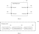
- FIG. 4 shows a structure of the input/output port according to an embodiment of the present invention.
- the input/output port 103 is a USB port (which may also be expressed as a USB port), and belongs to serial communications.
- a first end 401 of the USB port is connected to a power supply V BUS of a power adapter, and a second end 402 of the USB port is separately coupled to a first external connection end 209 of the power conversion circuit 101 and a first external connection end 307 of the information collection and signal control circuit 102.
- the second end 402 transfers energy of the power supply V BUS to the power conversion circuit 101 and the information collection and signal control circuit 102.
- a third end 403 of the USB port is connected to a data line of the power adapter.
- a fourth end 404 of the USB port is coupled to a second external connection end 308 of the information collection and signal control circuit 102.
- the fourth end 404 transfers a high or low level to implement data reading and writing for the information collection and signal control circuit 102.
- FIG. 5 shows a charging system 500 according to an embodiment of the present invention.
- the charging system 500 includes: a charging apparatus 100, a power adapter 501, and a battery element 502.
- One end of the power adapter 501 is connected to an external power supply, and the other end of the power adapter 501 is connected to an input/output port 103 of the charging apparatus 100.
- the power adapter 501 is configured to convert the external power supply into a power supply V BUS required by the charging apparatus 100. Then energy of the power supply V BUS is output to the charging apparatus 100 through a power cable.
- Output types may be classified into an alternating-current output type and a direct-current output type.
- the power adapter 501 is further configured to implement data communication and exchange with the charging apparatus 100 through a data line.
- the charging apparatus 100 may be an independent apparatus, or may be disposed inside a device, where the device may be a device such as a terminal, a base station, or an electric vehicle.
- the terminal may be a mobile phone (also referred to as a smartphone), a tablet computer (Tablet Personal Computer), a personal digital assistant (personal digital assistant, PDA), an electronic book reader (e-book reader), a wearable device (wearable device), or the like.
- the base station may include a macro base station, a micro base station (also referred to as a small cell), a relay station, an access point, or the like in various forms.
- the charging apparatus 100 is connected to the battery element 502, and is configured to charge a battery by using obtained energy.
- the device may further include the battery element 502, and the battery element 502 may include one or more batteries. If the battery element 502 includes a plurality of batteries, the plurality of batteries may be connected in series or in parallel. This is not limited in this embodiment of the present invention.
- constituent parts included in the charging apparatus and the charging system in this application are expressed as "xx elements". This expression presents each constituent part from a perspective of a function, but does not limit an implementation form of the constituent part.
- each constituent part may be implemented by a physical device, or a chip, or a circuit or an integrated circuit. This is not limited in this embodiment of the present invention.
- the power conversion circuit in FIG. 2 includes at least six switch elements.
- a composition structure of the power conversion circuit enables the charging apparatus to support battery charging in different charging modes. The following describes the technical solutions provided in the embodiments of the present invention by using different charging modes as examples and with reference to the foregoing descriptions of the charging apparatus.
- the power conversion circuit is configured to charge the battery in a low-voltage large-current mode.
- the second switch element and the sixth switch element in the power conversion circuit are always kept open, and the fifth switch element is always kept closed.
- the "kept open” because an open switch element has very large impedance, from a perspective of an actual effect, this is similar to that the open switch element is not connected to other elements.
- the "kept closed” because a closed switch element has very small impedance, from a perspective of an actual effect, this is similar to that the closed switch element is connected to another element through a conductor.
- an effective operating circuit structure of the power conversion circuit actually includes the first switch element, the third switch element, the fourth switch element, the first energy storage element, and the second energy storage element.
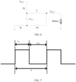
- FIG. 6 shows the effective operating circuit structure of the power conversion circuit in the first charging mode according to an embodiment of the present invention.
- the first switch element is denoted as Q 1
- the third switch element is denoted as Q 3
- the fourth switch element is denoted as Q 4
- the first energy storage element is a capacitor C FLY
- the second energy storage element is an inductor L.
- a first end of the capacitor C FLY is connected to a power supply V BUS through the switch element Q 1 , the first end of the capacitor C FLY is further connected to the inductor L, a second end of the capacitor C FLY is grounded through the switch element Q 3 , the second end of the capacitor C FLY is connected to a second end of the inductor L through the switch element Q 4 , the second end of the inductor L is coupled and connected to a positive end of a battery element (a battery shown in FIG. 6 ), and a negative end of the battery element is grounded.
- a battery element a battery shown in FIG. 6
- FIG. 7 shows a control signal time sequence of the power conversion circuit according to an embodiment of the present invention.
- a complete control signal period T includes two time periods: a first time period t ON and a second time period t OFF .
- the switch element Q 1 and the switch element Q 4 are in a closed state
- the switch element Q 3 is in an open state
- the input power supply V BUS is connected to the capacitor C FLY and then connected to a battery V BAT
- the input power supply V BUS is connected to the inductor L and then connected to the battery V BAT .
- the capacitor C FLY and the inductor L are in a charging and energy storage state.
- the switch element Q 1 and the switch element Q 4 are in an open state, the switch element Q 3 is in a closed state, a lower plate of the capacitor C FLY is grounded through the switch element Q 3 , and a voltage of an upper plate of the capacitor C FLY is V BUS - V BAT .
- the capacitor C FLY and the inductor L are in a discharging state, and charge the battery element.
- the first charging mode is usually applicable to a case in which a power adapter supports a 5 V/2 A power supply.
- the charging apparatus charges the battery in the first charging mode by using the power conversion circuit.
- a charging voltage of the battery is V BUS - V BAT , and the voltage is not high (for example, 5 V).
- An energy loss of an inductive winding in the circuit is relatively low, and an energy loss at a junction between the capacitor C FLY and the inductor L is relatively low, so that an overall energy loss of the power conversion circuit is relatively low when the power conversion circuit is charging the battery.
- a current input to the battery increases (for example, 2 A), thereby effectively increasing a battery charging rate.
- the power conversion circuit in a second charging mode, is configured to charge the battery in a high-voltage large-current mode. Based on this mode, with reference to FIG. 2 , the fourth switch element and the fifth switch element in the power conversion circuit are always kept open, and the sixth switch element is always kept closed.
- an effective operating circuit structure of the power conversion circuit actually includes the first switch element, the second switch element, the third switch element, the first energy storage element, and the second energy storage element.
- FIG. 8 shows the effective operating circuit structure of the power conversion circuit in the second charging mode according to an embodiment of the present invention. In FIG.
- the first switch element is denoted as Q 1
- the second switch element is denoted as Q 2
- the third switch element is denoted as Q 3
- the first energy storage element is a capacitor C FLY
- the second energy storage element is an inductor L.
- a first end of the capacitor C FLY is connected to a power supply V BUS through the switch element Q 1
- the first end of the capacitor C FLY is further coupled and connected to a positive end of a battery element (a battery shown in FIG.
- the switch element Q 1 in the first time period t ON , the switch element Q 1 is in a closed state, the switch element Q 2 and the switch element Q 3 are in an open state, the input power supply V BUS is connected to the capacitor C FLY , then connected to the inductor L, and then connected to a battery V BAT , and the capacitor C FLY and the inductor L are connected in series. In this case, the capacitor C FLY and the inductor L are in a charging and energy storage state.
- the switch element Q 1 In the second time period t OFF after the first time period t ON , the switch element Q 1 is in an open state, the switch element Q 2 and the switch element Q 3 are in a closed state, both a lower plate of the capacitor C FLY and a first end of the inductor are grounded, both an upper plate of the capacitor C FLY and a second end of the inductor L are connected to the battery V BAT , and the capacitor C FLY and the inductor L are connected in parallel. In this case, the capacitor C FLY and the inductor L are in a discharging state, and charge the battery element.
- the second charging mode is usually applicable to a case in which a power adapter supports a voltage of 9 V or 12 V
- the charging apparatus charges the battery in the second charging mode by using the power conversion circuit.
- a charging voltage of the battery is a difference between voltages at two ends of the capacitor C FLY and the inductor L, and usually, the charging voltage is relatively high (for example, 9 V or 12 V).
- An energy loss of an inductive winding in the circuit is relatively low, and an energy loss at a junction between the capacitor C FLY and the inductor L is relatively low, so that an overall energy loss of the power conversion circuit is relatively low when the power conversion circuit is charging the battery.
- a current input to the battery increases (for example, 2 A), thereby effectively increasing a battery charging rate.
- the power conversion circuit is configured to charge the battery in a high-voltage direct-charge mode.
- the fifth switch element and the sixth switch element in the power conversion circuit are always kept open, so that the second energy storage element is always in a non-operating state.
- an effective operating circuit structure of the power conversion circuit actually includes the first switch element, the second switch element, the third switch element, the fourth switch element, and the first energy storage element.
- FIG. 9 shows a structure of the power conversion circuit based on the third charging mode according to an embodiment of the present invention. In FIG.
- the first switch element is denoted as Q 1
- the second switch element is denoted as Q 2
- the third switch element is denoted as Q 3
- the fourth switch element is denoted as Q 4
- the first energy storage element is a capacitor C FLY .
- a first end of the capacitor C FLY is connected to a power supply V BUS through the switch element Q 1
- the first end of the capacitor C FLY is further coupled and connected to a positive end of a battery element (a battery shown in FIG.
- the switch element Q 1 and the switch element Q 4 are in a closed state, the switch element Q 2 and the switch element Q 3 are in an open state, and the input power supply V BUS is connected to the capacitor C FLY and then connected to a battery V BAT .
- the capacitor C FLY is in a charging and energy storage state.
- the switch element Q 1 and the switch element Q 4 are in an open state, the switch element Q 2 and the switch element Q 3 are in a closed state, a lower plate of the capacitor C FLY is grounded, and an upper plate of the capacitor C FLY is connected to the battery V BAT .
- the capacitor C FLY is in a discharging state, and charges the battery element.
- the charging apparatus charges the battery in the third charging mode by using the power conversion circuit.
- the first time period t ON two ends of the capacitor C FLY are separately directly connected to the power supply V BUS and the battery V BAT ; and in the second time period t OFF , a charging voltage of the battery is a difference between voltages at two ends of the capacitor C FLY . Therefore, this direct-charge and direct-discharge mode of the charging circuit leads to very high battery charging efficiency.
- the third charging mode is usually applicable to a case in which a power adapter supports a relatively high voltage (for example, 9 V or 12 V).
- the charging apparatus charges the battery in the third charging mode by using the power conversion circuit.
- the charging voltage of the battery is the difference between the voltages at the two ends of the capacitor C FLY . Because the input power supply V BUS directly charges the capacitor C FLY , charging efficiency of the capacitor is relatively high, and energy input to the battery directly sources from charging energy of the capacitor, so that a voltage of the input power supply approaches twice a voltage of the battery. In this high-voltage direct-charge case, an energy loss is relatively low, and the battery is likely to be fully charged with electricity fast, thereby effectively increasing a battery charging rate.
- the power conversion circuit is configured to charge the battery in a low-voltage direct-charge mode.
- the fourth switch element, the fifth switch element, and the sixth switch element in the power conversion circuit are always kept open, and the first switch element and the third switch element are always kept closed, so that the first energy storage element and the second energy storage element are always in a non-operating state.
- one end of the second switch element is coupled and connected to a power supply V BUS
- the other end of the second switch element is coupled and connected to a positive end of a battery
- a negative end of a battery element is grounded.
- the second switch element in the first time period t ON , the second switch element is in a closed state, and the input power supply V BUS is connected to a battery V BAT . In this case, the battery element is directly charged.
- the second time period t OFF the second switch element is in an open state, and charging of the battery element is suspended.
- the fourth charging mode is usually applicable to a case in which a power adapter supports a relatively low voltage (for example, 3 V or 5 V).
- the charging apparatus directly charges the battery with power energy through closing and opening of the second switch element in the power conversion circuit.
- a relatively low voltage for example, 3 V or 5 V.
- FIG. 10 shows another structure of the power conversion circuit according to an embodiment of the present invention.
- the power conversion circuit 101 is configured to convert a power supply V BUS into power energy required by a battery.
- the power conversion circuit 101 further includes a seventh switch element 211.
- a first end of the seventh switch element 211 is separately coupled to the second end of the first switch element 201, the first end of the second switch element 202, the first end of the fifth switch element 205, and the first end of the first energy storage element 207.
- a second end of the seventh switch element 211 is separately coupled to the first end of the third switch element 203, the first end of the fourth switch element 204, the first end of the sixth switch element 206, and the second end of the first energy storage element 207.
- the power conversion circuit in FIG. 10 includes at least seven switch elements.
- a composition structure of the power conversion circuit enables the charging apparatus to support not only the foregoing four charging modes but also other charging modes, so as to charge the battery.
- the power conversion circuit charges the battery in a conventional mode.
- the power conversion circuit is similar to a typical BUCK circuit, and is usually applicable to a case in which a power adapter supports a voltage of 5 V, 9 V, or 12 V.
- the fifth charging mode or the sixth charging mode with reference to FIG. 10 , in the fifth charging mode, the second switch element, the fourth switch element, and the sixth switch element in the power conversion circuit are always kept open, and the fifth switch element and the seventh switch element are always kept closed; and in the sixth charging mode, the second switch element, the fourth switch element, and the fifth switch element in the power conversion circuit are always kept open, and the sixth switch element and the seventh switch element are always kept closed.
- the seventh switch element is always kept closed, so that the first energy storage element is short-circuited and is in a non-operating state.
- an effective operating circuit structure of the power conversion circuit actually includes the first switch element, the third switch element, and the second energy storage element.
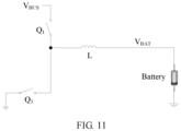
- FIG. 11 shows the effective operating circuit structure of the power conversion circuit in the fifth charging mode or the sixth charging mode according to an embodiment of the present invention.
- the first switch element is denoted as Q 1
- the third switch element is denoted as Q 3
- the second energy storage element is an inductor L.
- a first end of the inductor L is connected to a power supply V BUS through the switch element Q 1 , the first end of the inductor L is further grounded through the switch element Q 3 , a second end of the inductor L is coupled and connected to a positive end of a battery element (a battery shown in FIG. 11 ), and a negative end of the battery element is grounded.
- the switch element Q 1 in the first time period t ON , the switch element Q 1 is in a closed state, the switch element Q 3 is in an open state, and the input power supply V BUS is connected to the inductor L and then connected to a battery V BAT . In this case, the inductor L is in a charging and energy storage state.
- the switch element Q 1 is in an open state, the switch element Q 3 is in a closed state, and the inductor L is in a discharging state, and charges the battery element.
- the six switch elements or the seven switch elements, the first energy storage element, and the second energy storage element are not a mandatory composition structure of the power conversion circuit.
- An element quantity and a composition structure of the power conversion circuit may be pre-adjusted based on a supported charging mode.
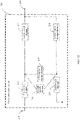
- FIG. 12 shows another structure of a power conversion circuit according to an embodiment of the present invention.
- the power conversion circuit 101 includes: a first switch element 201, a second switch element 202, a third switch element 203, a seventh switch element 211, a first energy storage element 207, and a second energy storage element 208.
- a first end of the first switch element 201 is coupled and connected to an input power supply through a first external connection end 209 of the power conversion circuit.
- a second end of the first switch element 201 is separately coupled to a first end of the second switch element 202, a first end of the seventh switch element 211, and a first end of the first energy storage element 207.
- a second end of the first energy storage element 207 is separately coupled to a first end of the second energy storage element 208, a first end of the third switch element 203, and a second end of the seventh switch element 211.
- a second end of the second switch element 202 is coupled and connected to a battery through a second external connection end 210 of the power conversion circuit.
- a second end of the second energy storage element 208 is coupled to the second external connection end 210.
- a second end of the third switch element 203 is grounded.
- the power conversion circuit 101 may charge the battery based on a second charging mode or a sixth charging mode. Specifically, in the second charging mode, in the power conversion circuit 101, the seventh switch element 211 is kept open; in a first time period, the first switch element 201 is in a closed state, the second switch element 202 and the third switch element 203 are in an open state, and the first energy storage element 207 and the second energy storage element 208 are charged; and in a second time period after the first time period, the first switch element 201 is in an open state, the second switch element 202 and the third switch element 203 are in a closed state, and the first energy storage element 207 and the second energy storage element 208 are discharged.
- the seventh switch element 211 in the power conversion circuit 101, the seventh switch element 211 is kept open; in a first time period, the first switch element 201 is in a closed state, the second switch element 202 and the third switch element 203 are in an open state, and the first energy storage element 207 and the second energy storage element 208 are
- the second switch element 202 is kept open, and the seventh switch element 211 is kept closed; in a first time period, the first switch element 201 is in a closed state, the third switch element 203 is in an open state, and the second energy storage element 208 is charged; and in a second time period after the first time period, the first switch element 201 is in an open state, the third switch element 203 is in a closed state, and the second energy storage element 208 is discharged.
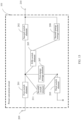
- FIG. 13 shows another structure of a power conversion circuit according to an embodiment of the present invention.
- the power conversion circuit 101 includes: a first switch element 201, a second switch element 202, a third switch element 203, a fifth switch element 205, a seventh switch element 211, a first energy storage element 207, and a second energy storage element 208.
- a first end of the first switch element 201 is coupled and connected to an input power supply through a first external connection end 209 of the power conversion circuit 101.
- a second end of the first switch element 201 is separately coupled to a first end of the second switch element 202, a first end of the fifth switch element 205, a first end of the seventh switch element 211, and a first end of the first energy storage element 207.
- a second end of the first energy storage element 207 is separately coupled to a first end of the third switch element 203 and a second end of the seventh switch element 211.
- a second end of the second switch element 202 is coupled and connected to a battery through a second external connection end 210 of the power conversion circuit 101.
- a second end of the fifth switch element 205 is connected to a first end of the second energy storage element 208.
- a second end of the second energy storage element 208 is coupled to the second external connection end 210.
- a second end of the third switch element 203 is grounded.
- the power conversion circuit may charge the battery based on a second charging mode, a fourth charging mode, a fifth charging mode, or a sixth charging mode.
- the second charging mode in the power conversion circuit 101, the fifth switch element 205 and the seventh switch element 211 are kept open; in a first time period, the first switch element 201 is in a closed state, the second switch element 202 and the third switch element 203 are in an open state, and the first energy storage element 207 and the second energy storage element 208 are charged; and in a second time period after the first time period, the first switch element 201 is in an open state, the second switch element 202 and the third switch element 203 are in a closed state, and the first energy storage element 207 and the second energy storage element 208 are discharged.
- the fifth switch element 205 and the seventh switch element 211 are kept open, and the first switch element 201 and the third switch element 203 are kept closed; in a first time period, the second switch element 202 is in a closed state, and the battery is directly charged; and in a second time period after the first time period, the second switch element 202 is in an open state, and battery charging is suspended.
- the second switch element 202 In the fifth charging mode, in the power conversion circuit 101, the second switch element 202 is kept open, and the fifth switch element 205 and the seventh switch element 211 are kept closed; in a first time period, the first switch element 201 is in a closed state, the third switch element 203 is in an open state, and the second energy storage element 208 is charged; and in a second time period after the first time period, the first switch element 201 is in an open state, the third switch element 203 is in a closed state, and the second energy storage element 208 is discharged.
- the second switch element 202 and the fifth switch element 205 are kept open, and the seventh switch element 211 is kept closed; in a first time period, the first switch element 201 is in a closed state, the third switch element 203 is in an open state, and the second energy storage element 208 is charged; and in a second time period after the first time period, the first switch element 201 is in an open state, the third switch element 203 is in a closed state, and the second energy storage element 208 is discharged.
- the power conversion circuit in FIG. 13 further includes a fourth switch element (not shown in the figure).
- a first end of the fourth switch element is separately coupled to the first end of the third switch element, the second end of the seventh switch element, and the second end of the first energy storage element.
- a second end of the fourth switch element is coupled to the second external connection end.
- the power conversion circuit may alternatively charge the battery based on a third charging mode.
- the fifth switch element in the third charging mode, in the power conversion circuit, the fifth switch element is kept open; in a first time period, the first switch element and the fourth switch element are in a closed state, the second switch element and the third switch element are in an open state, and the first energy storage element is charged; and in a second time period after the first time period, the first switch element and the fourth switch element are in an open state, the second switch element and the third switch element are in a closed state, and the first energy storage element is discharged.
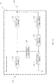
- FIG. 14 shows another structure of a power conversion circuit according to an embodiment of the present invention.
- the power conversion circuit 101 includes: a first switch element 201, a second switch element 202, a third switch element 203, a sixth switch element 206, a seventh switch element 211, a first energy storage element 207, and a second energy storage element 208.
- a first end of the first switch element 201 is coupled and connected to an input power supply through a first external connection end 209 of the power conversion circuit 101.
- a second end of the first switch element 201 is separately coupled to a first end of the second switch element 202, a first end of the seventh switch element 211, and a first end of the first energy storage element 207.
- a second end of the first energy storage element 207 is separately coupled to a first end of the third switch element 203, a first end of the sixth switch element 206, and a second end of the seventh switch element 211.
- a second end of the second switch element 202 is coupled and connected to a battery through a second external connection end 210 of the power conversion circuit 101.
- a second end of the sixth switch element 206 is connected to a first end of the second energy storage element 208.
- a second end of the second energy storage element 208 is coupled to the second external connection end 210.
- a second end of the third switch element 203 is grounded.
- the power conversion circuit may charge the battery based on a second charging mode, a fourth charging mode, or a sixth charging mode.
- the second charging mode in the power conversion circuit 101, the sixth switch element 206 is kept closed; in a first time period, the first switch element 201 is in a closed state, the second switch element 202 and the third switch element 203 are in an open state, and the first energy storage element 207 and the second energy storage element 208 are charged; and in a second time period after the first time period, the first switch element 201 is in an open state, the second switch element 202 and the third switch element 203 are in a closed state, and the first energy storage element 207 and the second energy storage element 208 are discharged.
- the sixth switch element 206 is kept open, and the first switch element 201 and the third switch element 203 are kept closed; in a first time period, the second switch element 202 is in a closed state, and the battery is directly charged; and in a second time period after the first time period, the second switch element 202 is in an open state, and battery charging is suspended.
- the second switch element 202 In the sixth charging mode, in the power conversion circuit 101, the second switch element 202 is kept open, and the sixth switch element 206 and the seventh switch element 211 are kept closed; in a first time period, the first switch element 201 is in a closed state, the third switch element 203 is in an open state, and the second energy storage element 208 is charged; and in a second time period after the first time period, the first switch element 201 is in an open state, the third switch element 203 is in a closed state, and the second energy storage element 208 is discharged.
- the power conversion circuit in FIG. 14 further includes a fourth switch element (not shown in the figure).
- a first end of the fourth switch element is separately coupled to the first end of the third switch element, the first end of the sixth switch element, the second end of the seventh switch element, and the second end of the first energy storage element.
- a second end of the fourth switch element is coupled to the second external connection end.
- the power conversion circuit may alternatively charge the battery based on a third charging mode.
- the sixth switch element in the third charging mode, in the power conversion circuit, the sixth switch element is kept open; in a first time period, the first switch element and the fourth switch element are in a closed state, the second switch element and the third switch element are in an open state, and the first energy storage element is charged; and in a second time period after the first time period, the first switch element and the fourth switch element are in an open state, the second switch element and the third switch element are in a closed state, and the first energy storage element is discharged.
- FIG. 15 shows another structure of a power conversion circuit according to an embodiment of the present invention.
- the power conversion circuit 101 includes: a first switch element 201, a second switch element 202, a third switch element 203, a fourth switch element 204, and a first energy storage element 207.
- a first end of the first switch element 201 is coupled and connected to an input power supply through a first external connection end 209 of the power conversion circuit 101.
- a second end of the first switch element 201 is separately coupled to a first end of the second switch element 202 and a first end of the first energy storage element 207.
- a second end of the first energy storage element 207 is separately coupled to a first end of the third switch element 203 and a first end of the fourth switch element 204.
- a second end of the second switch element 202 is coupled and connected to a battery through a second external connection end 210 of the power conversion circuit 101.
- a second end of the fourth switch element 204 is coupled to the second external connection end 210.
- a second end of the third switch element 203 is grounded.
- the power conversion circuit may charge the battery based on a third charging mode or a fourth charging mode.
- the third charging mode in the power conversion circuit 101, in a first time period, the first switch element 201 and the fourth switch element 204 are in a closed state, the second switch element 202 and the third switch element 203 are in an open state, and the first energy storage element 201 is charged; and in a second time period after the first time period, the first switch element 201 and the fourth switch element 204 are in an open state, the second switch element 202 and the third switch element 203 are in a closed state, and the first energy storage element 207 is discharged.
- the power conversion circuit in FIG. 15 further includes a fifth switch element and a second energy storage element (not shown in the figure).
- a first end of the fifth switch element is separately coupled to the second end of the first switch element, the first end of the second switch element, and the first end of the first energy storage element.
- a second end of the fifth switch element is connected to a first end of the second energy storage element.
- a second end of the second energy storage element is coupled to the second external connection end.
- the power conversion circuit may alternatively charge the battery based on a first charging mode.
- the second switch element in the first charging mode, in the power conversion circuit, the second switch element is kept open, and the fifth switch element is kept closed; in a first time period, the first switch element and the fourth switch element are in a closed state, the third switch element is in an open state, and the first energy storage element and the second energy storage element are charged; and in a second time period after the first time period, the first switch element and the fourth switch element are in an open state, the third switch element is in a closed state, and the first energy storage element and the second energy storage element are discharged.
- FIG. 16 shows another structure of a power conversion circuit according to an embodiment of the present invention.
- the power conversion circuit 101 includes: a first switch element 201, a second switch element 202, a third switch element 203, a sixth switch element 206, a first energy storage element 207, and a second energy storage element 208.
- a first end of the first switch element 201 is coupled and connected to an input power supply through a first external connection end 209 of the power conversion circuit 101.
- a second end of the first switch element 201 is separately coupled to a first end of the second switch element 202 and a first end of the first energy storage element 207.
- a second end of the first energy storage element 207 is separately coupled to a first end of the third switch element 203 and a first end of the sixth switch element 206.
- a second end of the second switch element 202 is coupled and connected to a battery through a second external connection end 210 of the power conversion circuit 101.
- a second end of the sixth switch element 206 is connected to a first end of the second energy storage element 208.
- a second end of the second energy storage element 208 is coupled to the second external connection end 210.
- a second end of the third switch element 203 is grounded.
- the power conversion circuit may charge the battery based on a second charging mode or a fourth charging mode.
- the second charging mode in the power conversion circuit 101, the sixth switch element 206 is kept closed; in a first time period, the first switch element 201 is in a closed state, the second switch element 202 and the third switch element 203 are in an open state, and the first energy storage element 207 and the second energy storage element 208 are charged; and in a second time period after the first time period, the first switch element 201 is in an open state, the second switch element 202 and the third switch element 203 are in a closed state, and the first energy storage element 207 and the second energy storage element 208 are discharged.
- the sixth switch element 206 is kept open, and the first switch element 201 and the third switch element 203 are kept closed; in a first time period, the second switch element 202 is in a closed state, and the battery is directly charged; and in a second time period after the first time period, the second switch element 202 is in an open state, and battery charging is suspended.
- the power conversion circuit in FIG. 16 further includes a fourth switch element (not shown in the figure).
- a first end of the fourth switch element is separately coupled to the first end of the third switch element, the first end of the sixth switch element, and the second end of the first energy storage element.
- a second end of the fourth switch element is coupled to the second external connection end.
- the power conversion circuit may alternatively charge the battery based on a third charging mode.
- the sixth switch element in the third charging mode, in the power conversion circuit, the sixth switch element is kept open; in a first time period, the first switch element and the fourth switch element are in a closed state, the second switch element and the third switch element are in an open state, and the first energy storage element is charged; and in a second time period after the first time period, the first switch element and the fourth switch element are in an open state, the second switch element and the third switch element are in a closed state, and the first energy storage element is discharged.
- FIG. 17 shows another structure of a power conversion circuit according to an embodiment of the present invention.
- the power conversion circuit 101 includes: a first switch element 201, a third switch element 203, a fourth switch element 204, a seventh switch element 211, a first energy storage element 207, and a second energy storage element 208.
- a first end of the first switch element 201 is coupled and connected to an input power supply through a first external connection end 209 of the power conversion circuit 101.
- a second end of the first switch element 201 is separately coupled to a first end of the seventh switch element 211, a first end of the first energy storage element 207, and a first end of the second energy storage element 208.
- a second end of the first energy storage element 207 is separately coupled to a first end of the third switch element 203, a first end of the fourth switch element 204, and a second end of the seventh switch element 211.
- a second end of the second energy storage element 208 is coupled and connected to a battery through a second external connection end 210 of the power conversion circuit 101.
- a second end of the fourth switch element 204 is coupled to the second external connection end 210.
- a second end of the third switch element 203 is grounded.
- the power conversion circuit may charge the battery based on a first charging mode or a fifth charging mode.
- the first charging mode in the power conversion circuit 101, in a first time period, the first switch element 201 and the fourth switch element 204 are in a closed state, the third switch element 203 is in an open state, and the first energy storage element 207 and the second energy storage element 208 are charged; and in a second time period after the first time period, the first switch element 201 and the fourth switch element 204 are in an open state, the third switch element 203 is in a closed state, and the first energy storage element 207 and the second energy storage element 208 are discharged.
- the fourth switch element 204 is kept open, and the seventh switch element 211 is kept closed; in a first time period, the first switch element 201 is in a closed state, the third switch element 203 is in an open state, and the second energy storage element 208 is charged; and in a second time period after the first time period, the first switch element 201 is in an open state, the third switch element 203 is in a closed state, and the second energy storage element 208 is discharged.
- FIG. 18 shows another structure of a power conversion circuit according to an embodiment of the present invention.
- the power conversion circuit 101 includes: a first switch element 201, a third switch element 203, a fourth switch element 204, a fifth switch element 205, a sixth switch element 206, a seventh switch element 211, a first energy storage element 207, and a second energy storage element 208.
- a first end of the first switch element 201 is coupled and connected to an input power supply through a first external connection end 209 of the power conversion circuit 101.
- a second end of the first switch element 201 is separately coupled to a first end of the fifth switch element 205, a first end of the seventh switch element 211, and a first end of the first energy storage element 207.
- a second end of the first energy storage element 207 is separately coupled to a first end of the third switch element 203, a first end of the fourth switch element 204, a first end of the sixth switch element 206, and a second end of the seventh switch element 211.
- a first end of the second energy storage element 208 is separately coupled to a second end of the fifth switch element 205 and a second end of the sixth switch element 206.
- a second end of the second energy storage element 208 is coupled and connected to a battery through a second external connection end 210 of the power conversion circuit 101.
- a second end of the fourth switch element 204 is coupled to the second external connection end 210.
- a second end of the third switch element 203 is grounded.
- the power conversion circuit may charge the battery based on a first charging mode, a fifth charging mode, or a sixth charging mode.
- the first charging mode in the power conversion circuit 101, the sixth switch element 206 is kept open, and the fifth switch element 205 is kept closed; in a first time period, the first switch element 201 and the fourth switch element 204 are in a closed state, the third switch element 203 is in an open state, and the first energy storage element 207 and the second energy storage element 208 are charged; and in a second time period after the first time period, the first switch element 201 and the fourth switch element 204 are in an open state, the third switch element 203 is in a closed state, and the first energy storage element 207 and the second energy storage element 208 are discharged.
- the fourth switch element 204 and the sixth switch element 206 are kept open, and the fifth switch element 205 and the seventh switch element 211 are kept closed; in a first time period, the first switch element 201 is in a closed state, the third switch element 203 is in an open state, and the second energy storage element 208 is charged; and in a second time period after the first time period, the first switch element 201 is in an open state, the third switch element 203 is in a closed state, and the second energy storage element 208 is discharged.
- the fourth switch element 204 and the fifth switch element 205 are kept open, and the sixth switch element 206 and the seventh switch element 211 are kept closed; in a first time period, the first switch element 201 is in a closed state, the third switch element 203 is in an open state, and the second energy storage element 208 is charged; and in a second time period after the first time period, the first switch element 201 is in an open state, the third switch element 203 is in a closed state, and the second energy storage element 208 is discharged.
- magnitude of a gate voltage of the switch element may be changed to close or open the switch element.
- the first end of the switch element Q 1 is coupled and connected to the power supply V BUS , and the second end of the switch element Q 1 is connected to another element.
- a gate voltage of the switch element Q 1 is increased, so that the gate voltage is higher than a voltage at the second end of the switch element Q 1 .
- the switch element Q 1 is in a low-resistance conducting state.
- the charging apparatus determines that the switch element Q 1 needs to be opened, the gate voltage of the switch element Q 1 is decreased, so that the gate voltage is lower than the voltage at the second end of the switch element Q 1 . In this case, the switch element Q 1 is in a high-resistance cut-off state. Because types of switch elements are different, correspondingly, implementations of closing or opening the switch elements are different. This is not limited in the embodiments of the present invention.
- the input/output port 103 of the charging apparatus 100 is connected to the power adapter 501 to obtain the input power supply V BUS , and then separately provides power energy for the power conversion circuit 101 and the information collection and signal control circuit 102.
- the digital core processing element 301 in the information collection and signal control circuit 102 performs protocol-based communication with the power adapter 501 through the input/output port 103; and then determines, based on a charging mode supported by the power adapter 501, a charging mode used by the power conversion circuit 101.
- the digital core processing element 301 determines that the power adapter 501 supports the foregoing five charging modes; then determines, based on the electrical characteristic of the power supply V BUS that is collected by the information input element 304 and the battery system information collected by the battery information detection element 302, that the third charging mode of the five charging modes has a highest charging rate; and then sets a charging status to the third charging mode.
- the digital core processing element 301 determines that the power adapter 501 supports the first charging mode and the second charging mode; then determines, based on the electrical characteristic of the power supply V BUS that is collected by the information input element 304 and the battery system information collected by the battery information detection element 302, that the second charging mode of the two charging modes has a highest charging rate; and then sets a charging status to the second charging mode.
- the digital core processing element 301 performs protocol-based communication with the power adapter 501 through the input/output port 103; and drives, based on a determined charging mode, the power adapter 501 to adjust a power voltage and/or current input to the charging apparatus 100.
- the digital core processing element 301 drives closing or opening of each switch element in the power conversion circuit 101 through the output drive element 303 based on the determined charging mode, so that the charging apparatus 100 charges the battery element 502.
- the battery information detection element 302 detects that the battery element 502 is fully charged and then notifies the digital core processing element 301.
- the digital core processing element 301 performs protocol-based communication with the power adapter 501 through the input/output port 103; drives the power adapter 501 to adjust, to 5 V, a voltage input to the charging apparatus 100; and then drives, through the output drive element 303, the power conversion circuit 101 to exit the used charging mode. Because the input/output port 103 is usually a USB port, a standard voltage of the input/output port 103 is 5 V by default.
- a circuit structure of the charging apparatus can support a plurality of different charging modes, so that the battery can be charged more quickly, thereby effectively improving charging efficiency.
- a is connected to B may indicate that A is directly connected to B, or A is indirectly connected to B.
- the disclosed system, apparatus, and method may be implemented in other manners.
- the element division is merely logical function division, and there may be other division manners in actual implementation.
- a plurality of elements may be combined or integrated into another system, or some features may be ignored or not performed.
- the shown or discussed mutual couplings or communication connections may be implemented by using some interfaces.
- the indirect couplings or communication connections between the apparatuses or units may be implemented in electrical, mechanical, or other forms.
Landscapes
- Engineering & Computer Science (AREA)
- Power Engineering (AREA)
- Theoretical Computer Science (AREA)
- Physics & Mathematics (AREA)
- General Engineering & Computer Science (AREA)
- General Physics & Mathematics (AREA)
- Charge And Discharge Circuits For Batteries Or The Like (AREA)
- Electric Propulsion And Braking For Vehicles (AREA)
- Dc-Dc Converters (AREA)
Applications Claiming Priority (3)
| Application Number | Priority Date | Filing Date | Title |
|---|---|---|---|
| CN201710429394.6A CN109038694B (zh) | 2017-06-08 | 2017-06-08 | 电源转换电路、充电装置及系统 |
| EP18813483.7A EP3627650B1 (de) | 2017-06-08 | 2018-06-07 | Stromversorgungswandlungsschaltung, ladevorrichtung und system |
| PCT/CN2018/090279 WO2018224010A1 (zh) | 2017-06-08 | 2018-06-07 | 电源转换电路、充电装置及系统 |
Related Parent Applications (2)
| Application Number | Title | Priority Date | Filing Date |
|---|---|---|---|
| EP18813483.7A Division EP3627650B1 (de) | 2017-06-08 | 2018-06-07 | Stromversorgungswandlungsschaltung, ladevorrichtung und system |
| EP18813483.7A Division-Into EP3627650B1 (de) | 2017-06-08 | 2018-06-07 | Stromversorgungswandlungsschaltung, ladevorrichtung und system |
Publications (2)
| Publication Number | Publication Date |
|---|---|
| EP4131714A2 true EP4131714A2 (de) | 2023-02-08 |
| EP4131714A3 EP4131714A3 (de) | 2023-04-26 |
Family
ID=64566354
Family Applications (2)
| Application Number | Title | Priority Date | Filing Date |
|---|---|---|---|
| EP18813483.7A Active EP3627650B1 (de) | 2017-06-08 | 2018-06-07 | Stromversorgungswandlungsschaltung, ladevorrichtung und system |
| EP22176915.1A Pending EP4131714A3 (de) | 2017-06-08 | 2018-06-07 | Leistungswandlerschaltung sowie ladegerät und system |
Family Applications Before (1)
| Application Number | Title | Priority Date | Filing Date |
|---|---|---|---|
| EP18813483.7A Active EP3627650B1 (de) | 2017-06-08 | 2018-06-07 | Stromversorgungswandlungsschaltung, ladevorrichtung und system |
Country Status (4)
| Country | Link |
|---|---|
| US (2) | US11404895B2 (de) |
| EP (2) | EP3627650B1 (de) |
| CN (1) | CN109038694B (de) |
| WO (1) | WO2018224010A1 (de) |
Families Citing this family (5)
| Publication number | Priority date | Publication date | Assignee | Title |
|---|---|---|---|---|
| CN106685219B (zh) * | 2017-02-28 | 2019-10-01 | 华为技术有限公司 | 电压转换器及其控制方法和电压转换系统 |
| CN109038694B (zh) * | 2017-06-08 | 2020-02-21 | 华为技术有限公司 | 电源转换电路、充电装置及系统 |
| CN112311101A (zh) | 2019-08-01 | 2021-02-02 | 北京小米移动软件有限公司 | 无线受电设备、无线充电方法及系统 |
| CN114598147A (zh) * | 2022-03-03 | 2022-06-07 | 珠海澳大科技研究院 | 降压直流-直流转换器、控制方法及电子设备 |
| CN115037011A (zh) * | 2022-04-19 | 2022-09-09 | 伏达半导体(合肥)有限公司 | 双电池充电装置、方法及其控制器 |
Family Cites Families (15)
| Publication number | Priority date | Publication date | Assignee | Title |
|---|---|---|---|---|
| US6304068B1 (en) * | 2000-04-20 | 2001-10-16 | City University Of Hong Kong | Bi-directional switched-capacitor based voltage converter |
| US7812579B2 (en) * | 2006-12-30 | 2010-10-12 | Advanced Analogic Technologies, Inc. | High-efficiency DC/DC voltage converter including capacitive switching pre-converter and up inductive switching post-regulator |
| CN201369577Y (zh) * | 2008-12-18 | 2009-12-23 | 成都市华为赛门铁克科技有限公司 | 一种掉电保护装置及利用其实现的电子设备 |
| FR2959624A1 (fr) * | 2010-04-28 | 2011-11-04 | St Ericsson Sa | Circuit de conversion de tension continue |
| CN104052278B (zh) * | 2013-03-15 | 2018-10-16 | 马克西姆综合产品公司 | 多电平增压变换器拓扑、控制和软启动系统及方法 |
| US10903678B2 (en) * | 2014-10-21 | 2021-01-26 | Maxwell Technologies, Inc. | Apparatus and method for providing bidirectional voltage support |
| JP6164195B2 (ja) * | 2014-11-06 | 2017-07-19 | トヨタ自動車株式会社 | 電力変換器 |
| US9602057B1 (en) * | 2015-09-18 | 2017-03-21 | Samsung Electronics Co., Ltd | Apparatus for and method of a supply modulator for a power amplifier |
| US9893628B2 (en) * | 2015-10-30 | 2018-02-13 | Apple Inc. | AC-DC power converters with improved voltage output level transitions |
| CN205945143U (zh) * | 2016-08-15 | 2017-02-08 | 珠海市魅族科技有限公司 | 一种充电电路、系统及移动终端 |
| US10797500B2 (en) * | 2016-09-20 | 2020-10-06 | Richtek Technology Corporation | Charger circuit and capacitive power conversion circuit and charging control method thereof |
| US10177576B2 (en) * | 2016-09-20 | 2019-01-08 | Richtek Technology Corporation | Charger circuit and capacitive power conversion circuit and reverse blocking switch circuit thereof |
| US10181744B2 (en) * | 2016-09-20 | 2019-01-15 | Richtek Technology Corporation | Capacitive power conversion circuit and charging control method thereof |
| CN106685219B (zh) * | 2017-02-28 | 2019-10-01 | 华为技术有限公司 | 电压转换器及其控制方法和电压转换系统 |
| CN109038694B (zh) * | 2017-06-08 | 2020-02-21 | 华为技术有限公司 | 电源转换电路、充电装置及系统 |
-
2017
- 2017-06-08 CN CN201710429394.6A patent/CN109038694B/zh active Active
-
2018
- 2018-06-07 EP EP18813483.7A patent/EP3627650B1/de active Active
- 2018-06-07 WO PCT/CN2018/090279 patent/WO2018224010A1/zh not_active Ceased
- 2018-06-07 EP EP22176915.1A patent/EP4131714A3/de active Pending
-
2019
- 2019-12-06 US US16/706,030 patent/US11404895B2/en active Active
-
2022
- 2022-07-08 US US17/860,402 patent/US11811254B2/en active Active
Also Published As
| Publication number | Publication date |
|---|---|
| EP3627650A1 (de) | 2020-03-25 |
| EP3627650A4 (de) | 2020-05-13 |
| US20200112177A1 (en) | 2020-04-09 |
| WO2018224010A1 (zh) | 2018-12-13 |
| WO2018224010A9 (zh) | 2019-11-28 |
| US11811254B2 (en) | 2023-11-07 |
| US20230017143A1 (en) | 2023-01-19 |
| EP4131714A3 (de) | 2023-04-26 |
| US11404895B2 (en) | 2022-08-02 |
| EP3627650B1 (de) | 2022-07-27 |
| CN109038694B (zh) | 2020-02-21 |
| CN109038694A (zh) | 2018-12-18 |
Similar Documents
| Publication | Publication Date | Title |
|---|---|---|
| US11342774B2 (en) | Power conversion circuit, and charging apparatus and system | |
| US11811254B2 (en) | Power conversion circuit, and charging apparatus and system | |
| CN102340169A (zh) | 双电池供电电路 | |
| CN112311038A (zh) | 一种充放电保护电路、终端设备及电池放电控制方法 | |
| CN103560550A (zh) | 一种可同时给移动电子设备供电及充电装置 | |
| CN102255345A (zh) | 双电池供电电路 | |
| KR20220158817A (ko) | 하이브리드 배터리 시스템 | |
| CN103904698A (zh) | 一种电池单元、终端设备及电池单元配置方法 | |
| CN103326459B (zh) | 低电压直流电源切换电路及其直流电源 | |
| CN213754015U (zh) | 一种蓝牙耳机的充电电路、充电盒及充电系统 | |
| CN116545048A (zh) | 一种电池及用电系统 | |
| CN207766009U (zh) | 直流充电桩功率分配电路及充电桩 | |
| CN116667473B (zh) | 一种控制电路、电路控制方法和电子设备 | |
| CN112448424B (zh) | 终端 | |
| CN203983422U (zh) | 具有自我保护功能和可扩展性的大电流锂离子电池组 | |
| CN100547877C (zh) | 正负组合脉冲充电机的自动停充控制电路 | |
| CN209375162U (zh) | 一种安全性高的充电桩电源装置 | |
| CN223858856U (zh) | 双向电源预充电路和设备 | |
| CN105553054A (zh) | 多电源电子设备的电源管理装置和供电/充电管理方法 | |
| CN217135204U (zh) | 一种具备pd快充功能的锂离子电池组 | |
| CN203691029U (zh) | 具时间阶段控制的多功能智能型交换充电器 | |
| CN104143663A (zh) | 具有自我保护功能和可扩展性的大电流锂离子电池组 | |
| CN221009826U (zh) | 一种Power Delivery USB充电电池 | |
| CN210297548U (zh) | 兼容pd充电器的锂电池组 | |
| CN107732333B (zh) | 电门锁控制模块 |
Legal Events
| Date | Code | Title | Description |
|---|---|---|---|
| PUAI | Public reference made under article 153(3) epc to a published international application that has entered the european phase |
Free format text: ORIGINAL CODE: 0009012 |
|
| STAA | Information on the status of an ep patent application or granted ep patent |
Free format text: STATUS: REQUEST FOR EXAMINATION WAS MADE |
|
| 17P | Request for examination filed |
Effective date: 20220602 |
|
| AC | Divisional application: reference to earlier application |
Ref document number: 3627650 Country of ref document: EP Kind code of ref document: P |
|
| AK | Designated contracting states |
Kind code of ref document: A2 Designated state(s): AL AT BE BG CH CY CZ DE DK EE ES FI FR GB GR HR HU IE IS IT LI LT LU LV MC MK MT NL NO PL PT RO RS SE SI SK SM TR |
|
| PUAL | Search report despatched |
Free format text: ORIGINAL CODE: 0009013 |
|
| AK | Designated contracting states |
Kind code of ref document: A3 Designated state(s): AL AT BE BG CH CY CZ DE DK EE ES FI FR GB GR HR HU IE IS IT LI LT LU LV MC MK MT NL NO PL PT RO RS SE SI SK SM TR |
|
| RIC1 | Information provided on ipc code assigned before grant |
Ipc: H02M 7/483 20070101ALI20230320BHEP Ipc: H02M 3/07 20060101ALI20230320BHEP Ipc: H02M 3/158 20060101ALI20230320BHEP Ipc: G06F 1/26 20060101ALI20230320BHEP Ipc: H02J 7/02 20160101ALI20230320BHEP Ipc: H02J 7/00 20060101AFI20230320BHEP |
|
| STAA | Information on the status of an ep patent application or granted ep patent |
Free format text: STATUS: EXAMINATION IS IN PROGRESS |
|
| 17Q | First examination report despatched |
Effective date: 20241204 |