EP4131428A1 - Laminated photovoltaic device, and production method - Google Patents
Laminated photovoltaic device, and production method Download PDFInfo
- Publication number
- EP4131428A1 EP4131428A1 EP20929299.4A EP20929299A EP4131428A1 EP 4131428 A1 EP4131428 A1 EP 4131428A1 EP 20929299 A EP20929299 A EP 20929299A EP 4131428 A1 EP4131428 A1 EP 4131428A1
- Authority
- EP
- European Patent Office
- Prior art keywords
- layer
- crystalline silicon
- energy level
- silicon layer
- metal oxide
- Prior art date
- Legal status (The legal status is an assumption and is not a legal conclusion. Google has not performed a legal analysis and makes no representation as to the accuracy of the status listed.)
- Pending
Links
- 238000004519 manufacturing process Methods 0.000 title abstract description 10
- 229910021419 crystalline silicon Inorganic materials 0.000 claims abstract description 240
- 229910044991 metal oxide Inorganic materials 0.000 claims abstract description 161
- 150000004706 metal oxides Chemical group 0.000 claims abstract description 154
- 230000005641 tunneling Effects 0.000 claims abstract description 97
- 238000000034 method Methods 0.000 claims abstract description 59
- 230000008569 process Effects 0.000 claims abstract description 30
- 239000000463 material Substances 0.000 claims description 30
- XUIMIQQOPSSXEZ-UHFFFAOYSA-N Silicon Chemical compound [Si] XUIMIQQOPSSXEZ-UHFFFAOYSA-N 0.000 claims description 27
- 239000010703 silicon Substances 0.000 claims description 27
- 230000007704 transition Effects 0.000 claims description 25
- 238000000151 deposition Methods 0.000 claims description 24
- 230000003647 oxidation Effects 0.000 claims description 24
- 238000007254 oxidation reaction Methods 0.000 claims description 24
- 229910052710 silicon Inorganic materials 0.000 claims description 24
- GWEVSGVZZGPLCZ-UHFFFAOYSA-N Titan oxide Chemical compound O=[Ti]=O GWEVSGVZZGPLCZ-UHFFFAOYSA-N 0.000 claims description 22
- XLOMVQKBTHCTTD-UHFFFAOYSA-N Zinc monoxide Chemical compound [Zn]=O XLOMVQKBTHCTTD-UHFFFAOYSA-N 0.000 claims description 22
- OGIDPMRJRNCKJF-UHFFFAOYSA-N titanium oxide Inorganic materials [Ti]=O OGIDPMRJRNCKJF-UHFFFAOYSA-N 0.000 claims description 22
- 230000008021 deposition Effects 0.000 claims description 20
- 230000006870 function Effects 0.000 claims description 17
- 239000002243 precursor Substances 0.000 claims description 12
- 239000011787 zinc oxide Substances 0.000 claims description 12
- 238000006243 chemical reaction Methods 0.000 claims description 11
- 238000005245 sintering Methods 0.000 claims description 10
- 238000000137 annealing Methods 0.000 claims description 9
- 239000011148 porous material Substances 0.000 claims description 9
- -1 Group III elements Inorganic materials 0.000 claims description 8
- 239000000126 substance Substances 0.000 claims description 8
- XOLBLPGZBRYERU-UHFFFAOYSA-N tin dioxide Chemical compound O=[Sn]=O XOLBLPGZBRYERU-UHFFFAOYSA-N 0.000 claims description 8
- 229910001887 tin oxide Inorganic materials 0.000 claims description 8
- PXHVJJICTQNCMI-UHFFFAOYSA-N Nickel Chemical compound [Ni] PXHVJJICTQNCMI-UHFFFAOYSA-N 0.000 claims description 7
- 238000002347 injection Methods 0.000 claims description 7
- 239000007924 injection Substances 0.000 claims description 7
- 229910052814 silicon oxide Inorganic materials 0.000 claims description 7
- UQSXHKLRYXJYBZ-UHFFFAOYSA-N Iron oxide Chemical compound [Fe]=O UQSXHKLRYXJYBZ-UHFFFAOYSA-N 0.000 claims description 6
- 239000002086 nanomaterial Substances 0.000 claims description 6
- XEEYBQQBJWHFJM-UHFFFAOYSA-N Iron Chemical compound [Fe] XEEYBQQBJWHFJM-UHFFFAOYSA-N 0.000 claims description 5
- 239000011651 chromium Substances 0.000 claims description 4
- 239000010949 copper Substances 0.000 claims description 4
- 238000005289 physical deposition Methods 0.000 claims description 4
- 229910052684 Cerium Inorganic materials 0.000 claims description 3
- VYZAMTAEIAYCRO-UHFFFAOYSA-N Chromium Chemical compound [Cr] VYZAMTAEIAYCRO-UHFFFAOYSA-N 0.000 claims description 3
- RYGMFSIKBFXOCR-UHFFFAOYSA-N Copper Chemical compound [Cu] RYGMFSIKBFXOCR-UHFFFAOYSA-N 0.000 claims description 3
- QPLDLSVMHZLSFG-UHFFFAOYSA-N Copper oxide Chemical compound [Cu]=O QPLDLSVMHZLSFG-UHFFFAOYSA-N 0.000 claims description 3
- 239000005751 Copper oxide Substances 0.000 claims description 3
- CBENFWSGALASAD-UHFFFAOYSA-N Ozone Chemical compound [O-][O+]=O CBENFWSGALASAD-UHFFFAOYSA-N 0.000 claims description 3
- WGLPBDUCMAPZCE-UHFFFAOYSA-N Trioxochromium Chemical compound O=[Cr](=O)=O WGLPBDUCMAPZCE-UHFFFAOYSA-N 0.000 claims description 3
- XHCLAFWTIXFWPH-UHFFFAOYSA-N [O-2].[O-2].[O-2].[O-2].[O-2].[V+5].[V+5] Chemical compound [O-2].[O-2].[O-2].[O-2].[O-2].[V+5].[V+5] XHCLAFWTIXFWPH-UHFFFAOYSA-N 0.000 claims description 3
- 229910052783 alkali metal Inorganic materials 0.000 claims description 3
- CXKCTMHTOKXKQT-UHFFFAOYSA-N cadmium oxide Inorganic materials [Cd]=O CXKCTMHTOKXKQT-UHFFFAOYSA-N 0.000 claims description 3
- CFEAAQFZALKQPA-UHFFFAOYSA-N cadmium(2+);oxygen(2-) Chemical compound [O-2].[Cd+2] CFEAAQFZALKQPA-UHFFFAOYSA-N 0.000 claims description 3
- KOPBYBDAPCDYFK-UHFFFAOYSA-N caesium oxide Chemical compound [O-2].[Cs+].[Cs+] KOPBYBDAPCDYFK-UHFFFAOYSA-N 0.000 claims description 3
- 229910001942 caesium oxide Inorganic materials 0.000 claims description 3
- GWXLDORMOJMVQZ-UHFFFAOYSA-N cerium Chemical compound [Ce] GWXLDORMOJMVQZ-UHFFFAOYSA-N 0.000 claims description 3
- 229910052804 chromium Inorganic materials 0.000 claims description 3
- 229910000423 chromium oxide Inorganic materials 0.000 claims description 3
- 229910017052 cobalt Inorganic materials 0.000 claims description 3
- 239000010941 cobalt Substances 0.000 claims description 3
- GUTLYIVDDKVIGB-UHFFFAOYSA-N cobalt atom Chemical compound [Co] GUTLYIVDDKVIGB-UHFFFAOYSA-N 0.000 claims description 3
- 229910000428 cobalt oxide Inorganic materials 0.000 claims description 3
- IVMYJDGYRUAWML-UHFFFAOYSA-N cobalt(ii) oxide Chemical compound [Co]=O IVMYJDGYRUAWML-UHFFFAOYSA-N 0.000 claims description 3
- 229910052802 copper Inorganic materials 0.000 claims description 3
- 229910000431 copper oxide Inorganic materials 0.000 claims description 3
- HTXDPTMKBJXEOW-UHFFFAOYSA-N dioxoiridium Chemical compound O=[Ir]=O HTXDPTMKBJXEOW-UHFFFAOYSA-N 0.000 claims description 3
- 229910021480 group 4 element Inorganic materials 0.000 claims description 3
- 229910021478 group 5 element Inorganic materials 0.000 claims description 3
- 229910000449 hafnium oxide Inorganic materials 0.000 claims description 3
- WIHZLLGSGQNAGK-UHFFFAOYSA-N hafnium(4+);oxygen(2-) Chemical compound [O-2].[O-2].[Hf+4] WIHZLLGSGQNAGK-UHFFFAOYSA-N 0.000 claims description 3
- 150000004820 halides Chemical class 0.000 claims description 3
- 229910052736 halogen Inorganic materials 0.000 claims description 3
- 150000002367 halogens Chemical class 0.000 claims description 3
- 229910000457 iridium oxide Inorganic materials 0.000 claims description 3
- 230000001788 irregular Effects 0.000 claims description 3
- 239000007791 liquid phase Substances 0.000 claims description 3
- CPLXHLVBOLITMK-UHFFFAOYSA-N magnesium oxide Inorganic materials [Mg]=O CPLXHLVBOLITMK-UHFFFAOYSA-N 0.000 claims description 3
- 239000000395 magnesium oxide Substances 0.000 claims description 3
- AXZKOIWUVFPNLO-UHFFFAOYSA-N magnesium;oxygen(2-) Chemical compound [O-2].[Mg+2] AXZKOIWUVFPNLO-UHFFFAOYSA-N 0.000 claims description 3
- 229910000476 molybdenum oxide Inorganic materials 0.000 claims description 3
- 229910052759 nickel Inorganic materials 0.000 claims description 3
- 229910000480 nickel oxide Inorganic materials 0.000 claims description 3
- 229910000484 niobium oxide Inorganic materials 0.000 claims description 3
- URLJKFSTXLNXLG-UHFFFAOYSA-N niobium(5+);oxygen(2-) Chemical compound [O-2].[O-2].[O-2].[O-2].[O-2].[Nb+5].[Nb+5] URLJKFSTXLNXLG-UHFFFAOYSA-N 0.000 claims description 3
- 150000004767 nitrides Chemical class 0.000 claims description 3
- QGLKJKCYBOYXKC-UHFFFAOYSA-N nonaoxidotritungsten Chemical compound O=[W]1(=O)O[W](=O)(=O)O[W](=O)(=O)O1 QGLKJKCYBOYXKC-UHFFFAOYSA-N 0.000 claims description 3
- PQQKPALAQIIWST-UHFFFAOYSA-N oxomolybdenum Chemical compound [Mo]=O PQQKPALAQIIWST-UHFFFAOYSA-N 0.000 claims description 3
- GNRSAWUEBMWBQH-UHFFFAOYSA-N oxonickel Chemical compound [Ni]=O GNRSAWUEBMWBQH-UHFFFAOYSA-N 0.000 claims description 3
- RVTZCBVAJQQJTK-UHFFFAOYSA-N oxygen(2-);zirconium(4+) Chemical compound [O-2].[O-2].[Zr+4] RVTZCBVAJQQJTK-UHFFFAOYSA-N 0.000 claims description 3
- 229910052761 rare earth metal Inorganic materials 0.000 claims description 3
- 229910052712 strontium Inorganic materials 0.000 claims description 3
- CIOAGBVUUVVLOB-UHFFFAOYSA-N strontium atom Chemical compound [Sr] CIOAGBVUUVVLOB-UHFFFAOYSA-N 0.000 claims description 3
- 229910052723 transition metal Inorganic materials 0.000 claims description 3
- 229910001930 tungsten oxide Inorganic materials 0.000 claims description 3
- 229910001935 vanadium oxide Inorganic materials 0.000 claims description 3
- 229910001928 zirconium oxide Inorganic materials 0.000 claims description 3
- HCHKCACWOHOZIP-UHFFFAOYSA-N Zinc Chemical compound [Zn] HCHKCACWOHOZIP-UHFFFAOYSA-N 0.000 claims description 2
- QCWXUUIWCKQGHC-UHFFFAOYSA-N Zirconium Chemical compound [Zr] QCWXUUIWCKQGHC-UHFFFAOYSA-N 0.000 claims description 2
- 229910052742 iron Inorganic materials 0.000 claims description 2
- 239000011701 zinc Substances 0.000 claims description 2
- 229910052725 zinc Inorganic materials 0.000 claims description 2
- 229910052726 zirconium Inorganic materials 0.000 claims description 2
- 230000006798 recombination Effects 0.000 abstract description 10
- 238000005215 recombination Methods 0.000 abstract description 10
- 239000002800 charge carrier Substances 0.000 abstract 4
- 239000010408 film Substances 0.000 description 19
- VYPSYNLAJGMNEJ-UHFFFAOYSA-N silicon dioxide Inorganic materials O=[Si]=O VYPSYNLAJGMNEJ-UHFFFAOYSA-N 0.000 description 17
- 238000010521 absorption reaction Methods 0.000 description 14
- 238000002161 passivation Methods 0.000 description 14
- 229910021417 amorphous silicon Inorganic materials 0.000 description 13
- 230000000694 effects Effects 0.000 description 10
- 239000010409 thin film Substances 0.000 description 9
- 238000009792 diffusion process Methods 0.000 description 8
- 229910052681 coesite Inorganic materials 0.000 description 7
- 229910052906 cristobalite Inorganic materials 0.000 description 7
- 238000002425 crystallisation Methods 0.000 description 7
- 230000008025 crystallization Effects 0.000 description 7
- 230000005525 hole transport Effects 0.000 description 7
- 238000005240 physical vapour deposition Methods 0.000 description 7
- 239000000377 silicon dioxide Substances 0.000 description 7
- 229910052682 stishovite Inorganic materials 0.000 description 7
- 229910052905 tridymite Inorganic materials 0.000 description 7
- 238000006388 chemical passivation reaction Methods 0.000 description 6
- 150000002500 ions Chemical class 0.000 description 6
- 230000005012 migration Effects 0.000 description 6
- 238000013508 migration Methods 0.000 description 6
- 230000003287 optical effect Effects 0.000 description 5
- PNEYBMLMFCGWSK-UHFFFAOYSA-N aluminium oxide Inorganic materials [O-2].[O-2].[O-2].[Al+3].[Al+3] PNEYBMLMFCGWSK-UHFFFAOYSA-N 0.000 description 4
- 238000005452 bending Methods 0.000 description 4
- 239000000969 carrier Substances 0.000 description 4
- 239000011248 coating agent Substances 0.000 description 4
- 238000000576 coating method Methods 0.000 description 4
- 229910052593 corundum Inorganic materials 0.000 description 4
- 238000005137 deposition process Methods 0.000 description 4
- 229910001845 yogo sapphire Inorganic materials 0.000 description 4
- 230000009471 action Effects 0.000 description 3
- 230000004888 barrier function Effects 0.000 description 3
- 230000005540 biological transmission Effects 0.000 description 3
- 230000015572 biosynthetic process Effects 0.000 description 3
- 238000005234 chemical deposition Methods 0.000 description 3
- QNWMNMIVDYETIG-UHFFFAOYSA-N gallium(ii) selenide Chemical compound [Se]=[Ga] QNWMNMIVDYETIG-UHFFFAOYSA-N 0.000 description 3
- 239000000758 substrate Substances 0.000 description 3
- 238000010301 surface-oxidation reaction Methods 0.000 description 3
- 238000002834 transmittance Methods 0.000 description 3
- GRYLNZFGIOXLOG-UHFFFAOYSA-N Nitric acid Chemical compound O[N+]([O-])=O GRYLNZFGIOXLOG-UHFFFAOYSA-N 0.000 description 2
- 239000005083 Zinc sulfide Substances 0.000 description 2
- 238000009825 accumulation Methods 0.000 description 2
- QVGXLLKOCUKJST-UHFFFAOYSA-N atomic oxygen Chemical compound [O] QVGXLLKOCUKJST-UHFFFAOYSA-N 0.000 description 2
- 230000009286 beneficial effect Effects 0.000 description 2
- HVMJUDPAXRRVQO-UHFFFAOYSA-N copper indium Chemical compound [Cu].[In] HVMJUDPAXRRVQO-UHFFFAOYSA-N 0.000 description 2
- 230000007547 defect Effects 0.000 description 2
- 238000005516 engineering process Methods 0.000 description 2
- 230000006872 improvement Effects 0.000 description 2
- 229910052751 metal Inorganic materials 0.000 description 2
- 239000002184 metal Substances 0.000 description 2
- 238000001451 molecular beam epitaxy Methods 0.000 description 2
- 229910017604 nitric acid Inorganic materials 0.000 description 2
- 229910052760 oxygen Inorganic materials 0.000 description 2
- 239000001301 oxygen Substances 0.000 description 2
- SOQBVABWOPYFQZ-UHFFFAOYSA-N oxygen(2-);titanium(4+) Chemical group [O-2].[O-2].[Ti+4] SOQBVABWOPYFQZ-UHFFFAOYSA-N 0.000 description 2
- 239000000243 solution Substances 0.000 description 2
- 238000001771 vacuum deposition Methods 0.000 description 2
- 229910052984 zinc sulfide Inorganic materials 0.000 description 2
- MARUHZGHZWCEQU-UHFFFAOYSA-N 5-phenyl-2h-tetrazole Chemical compound C1=CC=CC=C1C1=NNN=N1 MARUHZGHZWCEQU-UHFFFAOYSA-N 0.000 description 1
- JBRZTFJDHDCESZ-UHFFFAOYSA-N AsGa Chemical compound [As]#[Ga] JBRZTFJDHDCESZ-UHFFFAOYSA-N 0.000 description 1
- 229910001218 Gallium arsenide Inorganic materials 0.000 description 1
- 229910002370 SrTiO3 Inorganic materials 0.000 description 1
- KTSFMFGEAAANTF-UHFFFAOYSA-N [Cu].[Se].[Se].[In] Chemical compound [Cu].[Se].[Se].[In] KTSFMFGEAAANTF-UHFFFAOYSA-N 0.000 description 1
- 230000008901 benefit Effects 0.000 description 1
- 230000003139 buffering effect Effects 0.000 description 1
- 238000004140 cleaning Methods 0.000 description 1
- 239000013078 crystal Substances 0.000 description 1
- 230000003247 decreasing effect Effects 0.000 description 1
- 239000003989 dielectric material Substances 0.000 description 1
- 239000011810 insulating material Substances 0.000 description 1
- MHWZQNGIEIYAQJ-UHFFFAOYSA-N molybdenum diselenide Chemical compound [Se]=[Mo]=[Se] MHWZQNGIEIYAQJ-UHFFFAOYSA-N 0.000 description 1
- 229910021423 nanocrystalline silicon Inorganic materials 0.000 description 1
- TWNQGVIAIRXVLR-UHFFFAOYSA-N oxo(oxoalumanyloxy)alumane Chemical compound O=[Al]O[Al]=O TWNQGVIAIRXVLR-UHFFFAOYSA-N 0.000 description 1
- 239000002245 particle Substances 0.000 description 1
- 238000000623 plasma-assisted chemical vapour deposition Methods 0.000 description 1
- 239000002096 quantum dot Substances 0.000 description 1
- 230000009467 reduction Effects 0.000 description 1
- 230000004044 response Effects 0.000 description 1
- VSZWPYCFIRKVQL-UHFFFAOYSA-N selanylidenegallium;selenium Chemical compound [Se].[Se]=[Ga].[Se]=[Ga] VSZWPYCFIRKVQL-UHFFFAOYSA-N 0.000 description 1
- HBMJWWWQQXIZIP-UHFFFAOYSA-N silicon carbide Chemical compound [Si+]#[C-] HBMJWWWQQXIZIP-UHFFFAOYSA-N 0.000 description 1
- 235000012239 silicon dioxide Nutrition 0.000 description 1
- ABTOQLMXBSRXSM-UHFFFAOYSA-N silicon tetrafluoride Chemical compound F[Si](F)(F)F ABTOQLMXBSRXSM-UHFFFAOYSA-N 0.000 description 1
- 230000003595 spectral effect Effects 0.000 description 1
- JBQYATWDVHIOAR-UHFFFAOYSA-N tellanylidenegermanium Chemical compound [Te]=[Ge] JBQYATWDVHIOAR-UHFFFAOYSA-N 0.000 description 1
- DRDVZXDWVBGGMH-UHFFFAOYSA-N zinc;sulfide Chemical compound [S-2].[Zn+2] DRDVZXDWVBGGMH-UHFFFAOYSA-N 0.000 description 1
Images

Classifications
-
- H—ELECTRICITY
- H10—SEMICONDUCTOR DEVICES; ELECTRIC SOLID-STATE DEVICES NOT OTHERWISE PROVIDED FOR
- H10K—ORGANIC ELECTRIC SOLID-STATE DEVICES
- H10K30/00—Organic devices sensitive to infrared radiation, light, electromagnetic radiation of shorter wavelength or corpuscular radiation
- H10K30/40—Organic devices sensitive to infrared radiation, light, electromagnetic radiation of shorter wavelength or corpuscular radiation comprising a p-i-n structure, e.g. having a perovskite absorber between p-type and n-type charge transport layers
-
- H—ELECTRICITY
- H10—SEMICONDUCTOR DEVICES; ELECTRIC SOLID-STATE DEVICES NOT OTHERWISE PROVIDED FOR
- H10F—INORGANIC SEMICONDUCTOR DEVICES SENSITIVE TO INFRARED RADIATION, LIGHT, ELECTROMAGNETIC RADIATION OF SHORTER WAVELENGTH OR CORPUSCULAR RADIATION
- H10F10/00—Individual photovoltaic cells, e.g. solar cells
- H10F10/10—Individual photovoltaic cells, e.g. solar cells having potential barriers
- H10F10/14—Photovoltaic cells having only PN homojunction potential barriers
- H10F10/142—Photovoltaic cells having only PN homojunction potential barriers comprising multiple PN homojunctions, e.g. tandem cells
-
- H—ELECTRICITY
- H10—SEMICONDUCTOR DEVICES; ELECTRIC SOLID-STATE DEVICES NOT OTHERWISE PROVIDED FOR
- H10F—INORGANIC SEMICONDUCTOR DEVICES SENSITIVE TO INFRARED RADIATION, LIGHT, ELECTROMAGNETIC RADIATION OF SHORTER WAVELENGTH OR CORPUSCULAR RADIATION
- H10F10/00—Individual photovoltaic cells, e.g. solar cells
- H10F10/10—Individual photovoltaic cells, e.g. solar cells having potential barriers
- H10F10/16—Photovoltaic cells having only PN heterojunction potential barriers
- H10F10/161—Photovoltaic cells having only PN heterojunction potential barriers comprising multiple PN heterojunctions, e.g. tandem cells
-
- H—ELECTRICITY
- H10—SEMICONDUCTOR DEVICES; ELECTRIC SOLID-STATE DEVICES NOT OTHERWISE PROVIDED FOR
- H10F—INORGANIC SEMICONDUCTOR DEVICES SENSITIVE TO INFRARED RADIATION, LIGHT, ELECTROMAGNETIC RADIATION OF SHORTER WAVELENGTH OR CORPUSCULAR RADIATION
- H10F10/00—Individual photovoltaic cells, e.g. solar cells
- H10F10/10—Individual photovoltaic cells, e.g. solar cells having potential barriers
- H10F10/17—Photovoltaic cells having only PIN junction potential barriers
- H10F10/172—Photovoltaic cells having only PIN junction potential barriers comprising multiple PIN junctions, e.g. tandem cells
-
- H—ELECTRICITY
- H10—SEMICONDUCTOR DEVICES; ELECTRIC SOLID-STATE DEVICES NOT OTHERWISE PROVIDED FOR
- H10F—INORGANIC SEMICONDUCTOR DEVICES SENSITIVE TO INFRARED RADIATION, LIGHT, ELECTROMAGNETIC RADIATION OF SHORTER WAVELENGTH OR CORPUSCULAR RADIATION
- H10F10/00—Individual photovoltaic cells, e.g. solar cells
- H10F10/10—Individual photovoltaic cells, e.g. solar cells having potential barriers
- H10F10/17—Photovoltaic cells having only PIN junction potential barriers
- H10F10/174—Photovoltaic cells having only PIN junction potential barriers comprising monocrystalline or polycrystalline materials
-
- H—ELECTRICITY
- H10—SEMICONDUCTOR DEVICES; ELECTRIC SOLID-STATE DEVICES NOT OTHERWISE PROVIDED FOR
- H10F—INORGANIC SEMICONDUCTOR DEVICES SENSITIVE TO INFRARED RADIATION, LIGHT, ELECTROMAGNETIC RADIATION OF SHORTER WAVELENGTH OR CORPUSCULAR RADIATION
- H10F10/00—Individual photovoltaic cells, e.g. solar cells
- H10F10/10—Individual photovoltaic cells, e.g. solar cells having potential barriers
- H10F10/19—Photovoltaic cells having multiple potential barriers of different types, e.g. tandem cells having both PN and PIN junctions
-
- H—ELECTRICITY
- H10—SEMICONDUCTOR DEVICES; ELECTRIC SOLID-STATE DEVICES NOT OTHERWISE PROVIDED FOR
- H10F—INORGANIC SEMICONDUCTOR DEVICES SENSITIVE TO INFRARED RADIATION, LIGHT, ELECTROMAGNETIC RADIATION OF SHORTER WAVELENGTH OR CORPUSCULAR RADIATION
- H10F71/00—Manufacture or treatment of devices covered by this subclass
-
- H—ELECTRICITY
- H10—SEMICONDUCTOR DEVICES; ELECTRIC SOLID-STATE DEVICES NOT OTHERWISE PROVIDED FOR
- H10F—INORGANIC SEMICONDUCTOR DEVICES SENSITIVE TO INFRARED RADIATION, LIGHT, ELECTROMAGNETIC RADIATION OF SHORTER WAVELENGTH OR CORPUSCULAR RADIATION
- H10F71/00—Manufacture or treatment of devices covered by this subclass
- H10F71/10—Manufacture or treatment of devices covered by this subclass the devices comprising amorphous semiconductor material
- H10F71/103—Manufacture or treatment of devices covered by this subclass the devices comprising amorphous semiconductor material including only Group IV materials
-
- H—ELECTRICITY
- H10—SEMICONDUCTOR DEVICES; ELECTRIC SOLID-STATE DEVICES NOT OTHERWISE PROVIDED FOR
- H10F—INORGANIC SEMICONDUCTOR DEVICES SENSITIVE TO INFRARED RADIATION, LIGHT, ELECTROMAGNETIC RADIATION OF SHORTER WAVELENGTH OR CORPUSCULAR RADIATION
- H10F71/00—Manufacture or treatment of devices covered by this subclass
- H10F71/121—The active layers comprising only Group IV materials
-
- H—ELECTRICITY
- H10—SEMICONDUCTOR DEVICES; ELECTRIC SOLID-STATE DEVICES NOT OTHERWISE PROVIDED FOR
- H10F—INORGANIC SEMICONDUCTOR DEVICES SENSITIVE TO INFRARED RADIATION, LIGHT, ELECTROMAGNETIC RADIATION OF SHORTER WAVELENGTH OR CORPUSCULAR RADIATION
- H10F77/00—Constructional details of devices covered by this subclass
- H10F77/10—Semiconductor bodies
- H10F77/12—Active materials
- H10F77/122—Active materials comprising only Group IV materials
-
- H—ELECTRICITY
- H10—SEMICONDUCTOR DEVICES; ELECTRIC SOLID-STATE DEVICES NOT OTHERWISE PROVIDED FOR
- H10F—INORGANIC SEMICONDUCTOR DEVICES SENSITIVE TO INFRARED RADIATION, LIGHT, ELECTROMAGNETIC RADIATION OF SHORTER WAVELENGTH OR CORPUSCULAR RADIATION
- H10F77/00—Constructional details of devices covered by this subclass
- H10F77/10—Semiconductor bodies
- H10F77/14—Shape of semiconductor bodies; Shapes, relative sizes or dispositions of semiconductor regions within semiconductor bodies
- H10F77/147—Shapes of bodies
-
- H—ELECTRICITY
- H10—SEMICONDUCTOR DEVICES; ELECTRIC SOLID-STATE DEVICES NOT OTHERWISE PROVIDED FOR
- H10F—INORGANIC SEMICONDUCTOR DEVICES SENSITIVE TO INFRARED RADIATION, LIGHT, ELECTROMAGNETIC RADIATION OF SHORTER WAVELENGTH OR CORPUSCULAR RADIATION
- H10F77/00—Constructional details of devices covered by this subclass
- H10F77/70—Surface textures, e.g. pyramid structures
- H10F77/703—Surface textures, e.g. pyramid structures of the semiconductor bodies, e.g. textured active layers
-
- H—ELECTRICITY
- H10—SEMICONDUCTOR DEVICES; ELECTRIC SOLID-STATE DEVICES NOT OTHERWISE PROVIDED FOR
- H10K—ORGANIC ELECTRIC SOLID-STATE DEVICES
- H10K39/00—Integrated devices, or assemblies of multiple devices, comprising at least one organic radiation-sensitive element covered by group H10K30/00
- H10K39/10—Organic photovoltaic [PV] modules; Arrays of single organic PV cells
- H10K39/15—Organic photovoltaic [PV] modules; Arrays of single organic PV cells comprising both organic PV cells and inorganic PV cells
-
- H—ELECTRICITY
- H10—SEMICONDUCTOR DEVICES; ELECTRIC SOLID-STATE DEVICES NOT OTHERWISE PROVIDED FOR
- H10K—ORGANIC ELECTRIC SOLID-STATE DEVICES
- H10K85/00—Organic materials used in the body or electrodes of devices covered by this subclass
- H10K85/50—Organic perovskites; Hybrid organic-inorganic perovskites [HOIP], e.g. CH3NH3PbI3
-
- Y—GENERAL TAGGING OF NEW TECHNOLOGICAL DEVELOPMENTS; GENERAL TAGGING OF CROSS-SECTIONAL TECHNOLOGIES SPANNING OVER SEVERAL SECTIONS OF THE IPC; TECHNICAL SUBJECTS COVERED BY FORMER USPC CROSS-REFERENCE ART COLLECTIONS [XRACs] AND DIGESTS
- Y02—TECHNOLOGIES OR APPLICATIONS FOR MITIGATION OR ADAPTATION AGAINST CLIMATE CHANGE
- Y02E—REDUCTION OF GREENHOUSE GAS [GHG] EMISSIONS, RELATED TO ENERGY GENERATION, TRANSMISSION OR DISTRIBUTION
- Y02E10/00—Energy generation through renewable energy sources
- Y02E10/50—Photovoltaic [PV] energy
- Y02E10/549—Organic PV cells
-
- Y—GENERAL TAGGING OF NEW TECHNOLOGICAL DEVELOPMENTS; GENERAL TAGGING OF CROSS-SECTIONAL TECHNOLOGIES SPANNING OVER SEVERAL SECTIONS OF THE IPC; TECHNICAL SUBJECTS COVERED BY FORMER USPC CROSS-REFERENCE ART COLLECTIONS [XRACs] AND DIGESTS
- Y02—TECHNOLOGIES OR APPLICATIONS FOR MITIGATION OR ADAPTATION AGAINST CLIMATE CHANGE
- Y02P—CLIMATE CHANGE MITIGATION TECHNOLOGIES IN THE PRODUCTION OR PROCESSING OF GOODS
- Y02P70/00—Climate change mitigation technologies in the production process for final industrial or consumer products
- Y02P70/50—Manufacturing or production processes characterised by the final manufactured product
Definitions
- the disclosure relates to the technical field of photovoltaics, in particular to a tandem photovoltaic device and a producing method for the same.
- tandem photovoltaic devices sunlight can be divided into multiple bands and units of a solar cell with gradually decreasing band gaps from front to back are adopted to absorb sunlight with different energies, so as to broaden a spectral response band to sunlight and reduce energy loss. Therefore, the tandem photovoltaic devices present wide application prospect.
- the tandem photovoltaic devices with a crystalline silicon cell as a lower cell unit have a large space for mass production.
- a tunnel junction has strong recombination ability and its thickness required to achieve high recombination rate is relatively small. Therefore, the tunnel junction is usually adopted to connect respective cell units in series in the tandem photovoltaic devices.
- the tunnel junction of the tandem photovoltaic devices with the crystalline silicon cell as the lower cell unit is with a complicated process, serious interface recombination, large overall series resistance, and low tunneling efficiency.
- a tandem photovoltaic device and a producing method for the same are provided in the present disclosure, aiming at solving problems of complicated process, serious interface recombination, large overall series resistance and low tunneling efficiency in the tandem photovoltaic device.
- a tandem photovoltaic device including an upper cell unit and a lower cell unit, and a tunnel junction located between the upper cell unit and the lower cell unit; and the lower cell unit is a crystalline silicon cell;
- a conductivity type of the metal oxide layer is different from that of the crystalline silicon layer.
- the metal oxide layer is made of a material selected from metal oxides with work functions greater than or equal to 3 eV, when the crystalline silicon layer is a p-type crystalline silicon layer;
- the metal oxide layer is made of a material selected from n-type metal oxides with work functions greater than or equal to 5 eV or p-type metal oxides with work functions less than or equal to 6 eV, when the crystalline silicon layer is an n-type crystalline silicon layer.
- the metal oxide layer is made of a material selected from at least one of zinc oxide, tin oxide, titanium oxide, molybdenum oxide, vanadium oxide, tungsten oxide, chromium oxide, copper oxide and hafnium oxide, when the crystalline silicon layer is a p-type crystalline silicon layer; and the metal oxide layer is made of a material selected from at least one of nickel oxide, niobium oxide, iron oxide, cadmium oxide, iridium oxide, magnesium oxide, cesium oxide, cobalt oxide and zirconium oxide, when the crystalline silicon layer is an n-type crystalline silicon layer.
- the metal oxide layer is further doped with at least one of following elements: halogen elements, transition metal elements, alkali metal elements, rare earth elements, Group III elements, Group IV elements or Group V elements.
- the metal oxide layer is doped with at least one of following elements: strontium, chromium, iron, cobalt, nickel, copper, zinc, cerium and zirconium.
- the tunneling layer is made of a material selected from at least one of oxides of silicon, nitrides of silicon, oxynitrides of silicon, halides of silicon and metal oxides with a dielectric strength greater than 3 MV/cm.
- the intermediate layer further includes a first transition layer located between the tunneling layer and the metal oxide layer, and/or the intermediate layer further includes a second transition layer located between the tunneling layer and the crystalline silicon layer;
- the energy level at the bottom of the conduction band of the metal oxide layer is the same as the first energy level E1
- the energy level at the top of the valence band of the p-type crystalline silicon layer is the same as the second energy level E2
- the energy level at the top of the valence band of the metal oxide layer is the same as the third energy level E3
- the energy level at the bottom of the conduction band of the n-type crystalline silicon layer is the same as the fourth energy level E4.
- a first surface in contact with the shadow surface of the upper cell unit has a porous morphology, an irregular morphology or a nanostructure morphology, and a second surface in contact with the intermediate layer has a flat and compact morphology.
- thicknesses of the crystalline silicon layer and the metal oxide layer are both 2 nm to 100 nm; and a thickness of the intermediate layer is 0.1 nm to 5 nm.
- a light-facing surface of the lower cell unit is provided with a light-trapping structure, and a shadow surface of the tunnel junction is adapted to a shape of the light-facing surface of the lower cell unit.
- a producing method for a tandem photovoltaic device which includes following steps:
- the crystalline silicon layer is prepared with one of following processes:
- the metal oxide layer is prepared by:
- the step of preparing the tunnel junction further includes: performing a post-treating on the metal oxide layer, wherein the post-treating includes one of following processes: annealing, sintering, ultraviolet light treatment, light injection, electric injection, ozone oxidation and liquid phase treatment.
- the step of preparing the tunnel junction further includes:
- the lower cell unit is the crystalline silicon cell
- the tunnel junction includes the carrier transport layer, the crystalline silicon layer and the intermediate layer located between the carrier transport layer and the crystalline silicon layer.
- the carrier transport layer is the metal oxide layer.
- the intermediate layer includes a tunneling layer, and the carrier transport layer and the crystalline silicon layer are in direct contact with the intermediate layer, respectively.
- the carrier transport layer is directly contacted with the shadow surface of the upper cell unit, and the metal oxide layer can serve as a hole transport layer or an electron transport layer or a buffer layer of the upper cell unit, this facilitates realization of better connection performance, and additionally there is no need to separately provide the hole transport layer or the electron transport layer or the buffer layer for the upper cell unit, so that complexity of a whole structure and a number of interfaces can be reduced, the process complexity can be reduced, recombination, attenuation and the like generated when carriers cross the interfaces can be effectively reduced, and overall tunneling efficiency of a device structure can be improved. Meanwhile, the metal oxide layer and the crystalline silicon layer are quite different from each other and an abruptly doped interface structure is formed at an interface between them.
- the intermediate layer including the tunneling layer is added between the metal oxide layer and the crystalline silicon layer, which can further facilitate formation of the abruptly doped interface structure at the interface with barrier effect of the tunneling layer, so that the tunneling efficiency can be effectively improved, a series resistance of a tunnel junction can be reduced, and a peak tunnel current can be increased.
- energy level degeneracy can be realized without an extremely high doping concentration of the crystalline silicon layer, that is, the doping concentration of the crystalline silicon layer is greater than or equal to 10 17 cm -3 , which reduces bulk recombination of the crystalline silicon layer and facilitates improvement of the overall tunneling efficiency of the device.
- the intermediate layer including the tunneling layer inserted at the interface between the metal layer and the crystalline silicon layer, better chemical passivation can be realized.
- there is majority carrier accumulation on both sides of the intermediate layer including the tunneling layer in the tunnel junction which leads to bending of an energy band, improves the tunneling efficiency, and drives away minority carriers, thus achieving good field passivation effect.
- the energy level at the bottom of the conduction band of the metal oxide at the interface where the metal oxide layer contacts the intermediate layer and the energy level at the top of the valence band of the p-type crystalline silicon at the interface where the intermediate layer contacts the p-type crystalline silicon layer satisfy the relationship described above.
- the energy level at the top of the valence band of the metal oxide at the interface where the metal oxide layer contacts the intermediate layer, and the energy level at the bottom of the conduction band of the n-type crystalline silicon at the interface where the intermediate layer contacts the n-type crystalline silicon layer satisfy the relationship described above. That is, energy levels at both sides are matched at the interface regardless of the crystalline silicon layer being the p-type crystalline silicon layer or the n-type crystalline silicon layer, so that direct tunneling can be easily realized and the tunneling efficiency can be improved.
- 1- upper cell unit 11- perovskite coating, 12- hole transport layer, 13- ITO, 14- zinc sulfide layer, 15- copper indium gallium selenium absorption layer, 16- molybdenum selenide transport layer, 17- antireflection film, 2- lower cell unit, 21- n-type silicon wafer, 22- intrinsic amorphous silicon, 23- n-type amorphous silicon, 24- p+ layer, 25- p-type silicon wafer, 26- n+ layer, 27- PERx passivation structure, 3- tunnel junction, 4- top electrode, 5- bottom electrode, 31- metal oxide layer, 311- titanium oxide metal oxide layer, 312- aluminum-doped zinc oxide metal oxide layer, 32- crystalline silicon layer, 321- p++ layer, 33- intermediate layer, 331- SiO 2 tunneling layer, 332- Al 2 O 3 tunneling layer.
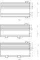
- FIG. 1 shows a first tandem photovoltaic device according to an embodiment of the present disclosure.
- the tandem photovoltaic device includes an upper cell unit 1 and a lower cell unit 2, and a tunnel junction 3 located between the upper cell unit 1 and the lower cell unit 2, and the tunnel junction 3 is configured for connecting the upper cell unit 1 and the lower cell unit 2 in series to form the tandem photovoltaic device.
- the upper cell unit 1 and the lower cell unit 2 have different band gaps, and a band gap of the upper cell unit 1 is larger than that of the lower cell unit 2.
- the lower cell unit is a crystalline silicon cell. Numbers of the tunnel junction, the upper cell unit and the lower cell unit included in the tandem photovoltaic device are not specifically limited in embodiments of the present disclosure.
- a top electrode is indicated by 4 and a bottom electrode is indicated by 5.
- the tunnel junction 3 has light transmittance for transmitting remaining wave bands after absorption by the upper cell unit.
- a light-transmission wave bands corresponds to the light transmittance can be determined according to the remaining lights after the absorption by the upper cell unit adjacent to the tunnel junction.
- this light-transmission wave bands corresponds to the light transmittance can be the remaining wave bands after the absorption by the upper cell unit adjacent to the tunnel junction.
- the tunnel junction 3 may include a carrier transport layer, a crystalline silicon layer 32, and an intermediate layer 33 located between the carrier transport layer and the crystalline silicon layer 32.
- the carrier transport layer is a metal oxide layer 31, which has property of carrier transmission.
- the intermediate layer 33 includes a tunneling layer. The carrier transport layer and the crystalline silicon layer 32 are in direct contact with the intermediate layer 33, respectively.
- the carrier transport layer is directly contacted with the shadow surface of the upper cell unit 1, and the metal oxide layer 31 can serve as a hole transport layer or an electron transport layer or a buffer layer of the upper cell unit 1, this facilitates realization of better connection performance, and additionally there is no need to separately provide the hole transport layer or the electron transport layer or the buffer layer for the upper cell unit 1, so that complexity of a whole structure and a number of interfaces can be reduced, process complexity can be reduced, recombination, attenuation and the like generated when carriers cross the interfaces can be effectively reduced, and overall tunneling efficiency of a device structure can be improved. Meanwhile, the metal oxide layer 31 and the crystalline silicon layer 32 are quite different from each other and an abruptly doped interface structure is formed at an interface between them.
- the intermediate layer 33 including the tunneling layer is added between the metal oxide layer 31 and the crystalline silicon layer 32, which can further facilitate formation of the abruptly doped interface structure at the interface with barrier effect of the tunneling layer, so that tunneling efficiency can be effectively improved, a series resistance of a tunnel junction can be reduced, and a peak tunnel current can be increased.
- the crystalline silicon layer 32 is in contact with the lower cell unit 2.
- a doping type of the silicon layer 32 is the same as that of a light-facing surface of the lower cell unit 2.
- the doping concentration of the crystalline silicon layer is greater than or equal to 10 17 cm -3 , which reduces bulk recombination of the crystalline silicon layer 32 and facilitates improvement of the overall tunneling efficiency of the device.
- a contact interface between the intermediate layer 33 including the tunneling layer and the crystalline silicon layer 32 and a contact interface between the intermediate layer 33 including the tunneling layer and the metal oxide layer 31 both have fixed charges or fixed defects, and majority carrier accumulation may occur at both sides of the intermediate layer 33 including the tunneling layer in the tunnel junction, which leads to band bending or band pinning of the crystalline silicon.
- band bending at the interface direct tunneling can be realized after the band bending, which improves the tunneling efficiency and drives away minority carriers, thus achieving good field passivation effect.
- the crystalline silicon layer 32 may be made of single crystal or polycrystalline.
- the crystalline silicon layer 32 may be a p -type crystalline silicon layer or an n-type crystalline silicon layer.
- the first energy level E1 and the second energy level E2 satisfy E1-E2 ⁇ 0.5 eV.
- the first energy level E1 is an energy level at a bottom of a conduction band of a metal oxide at an interface where the metal oxide layer 31 contacts the intermediate layer 33.
- the second energy level E2 is an energy level at a top of a valence band of a p-type crystalline silicon at an interface where the intermediate layer 33 contacts the p-type crystalline silicon layer.
- E1-E2 may be a positive number not greater than 0.5 eV, or zero, or a negative number.
- the first energy level E1 and the second energy level E2 can be as close or flush as possible. With the first energy level E1 and the second energy level E2 being closer to each other, matching of energy levels at both sides can be realized at the interface, so that direct tunneling can be easily realized, and the tunneling efficiency can be improved.
- energy levels at the bottom of the conduction band of the metal oxide at various positions in the metal oxide layer 31 may be the same or different.
- energy levels at the top of the valence band of the p-type crystalline silicon at various positions in the p-type crystalline silicon layer may be the same or different.
- the third energy level E3 is close to the fourth energy level E4.
- the third energy level E3 is an energy level at a top of a valence band of the metal oxide at an interface where the carrier transport layer contacts the intermediate layer 33.
- the fourth energy level E4 is an energy level at a bottom of a conduction band of the n-type crystalline silicon at an interface where the intermediate layer 33 contacts the n-type crystalline silicon layer.
- the third energy level E3 and the fourth energy level E4 can be as close or flush as possible.
- an absolute value of difference between the third energy level and the fourth energy level is not more than 0.5 eV.
- a value obtained by the third energy level E3 subtracting the fourth energy level E4 is not more than 0.5 eV, or a value obtained by the fourth energy level E4 subtracting the third energy level E3 is not more than 0.5 eV.
- the energy levels at the top of the valence band of the metal oxide at various positions in the metal oxide layer 31 may be the same or different.
- energy levels at the bottom of the conduction band of the n-type crystalline silicon at various positions in the n-type crystalline silicon layer may be the same or different.
- the first energy level is close to the second energy level.
- the third energy level is close to the fourth energy level. Further, matching of energy levels at both sides can be realized at the interface, so that direct tunneling can be easily realized, and the tunneling efficiency can be improved.
- the energy level at the bottom of the conduction band of the metal oxide layer 31 is the same as the first energy level E1
- the energy level at the top of the valence band of the p-type crystalline silicon layer is the same as the second energy level E2. That is, when the crystalline silicon layer 32 is the p-type crystalline silicon layer, the energy levels at the bottom of the conduction band of the metal oxide at various positions in the metal oxide layer 31 are equal, and the energy levels at the top of the valence band of the p-type crystalline silicon at various position in the p-type crystalline silicon layer are equal, so that it can be ensured sufficiently that the first energy level E1 is close to the second energy level E2.
- the energy level at the top of the valence band of the metal oxide layer is the same as the third energy level E3; and the energy level at the bottom of the conduction band of the n-type crystalline silicon layer is the same as the fourth energy level E4, when the crystalline silicon layer 32 is the n-type crystalline silicon layer. That is, when the crystalline silicon layer 32 is the n-type crystalline silicon layer, the energy levels at the top of the valence band of the metal oxide at various positions in the metal oxide layer 31 are equal, and the energy levels at the bottom of the conduction band of the n-type crystalline silicon at various position in the n-type crystalline silicon layer are equal, so that it can be ensured sufficiently that the third energy level E3 is close to the fourth energy level E4.
- the tunneling layer is made of a material selected from at least one of oxides of silicon, nitrides of silicon, oxynitrides of silicon, halides of silicon and metal oxides with a dielectric strength greater than 3 MV/cm, with a diversified material selection of the tunneling layer, and good passivation and tunneling effect.
- the tunneling layer can be made of silicon oxide, aluminum oxide, or silicon fluoride.
- the intermediate layer 33 further includes a first transition layer between the tunneling layer and the metal oxide layer 31, and/or the intermediate layer further includes a second transition layer between the tunneling layer and the crystalline silicon layer 32.
- the first transition layer is made of a material selected from at least one product of interface reactions (which are not limited to mutual doping or ion migration) between the tunneling layer and the metal oxide layer 31.
- the second transition layer is made of a material selected from at least one product of interface reactions (which are not limited to mutual doping or ion migration) between the tunneling layer and the crystalline silicon layer 32.
- the first transition layer and the second transition layer both can function in good chemical passivation of surfaces.
- the first transition layer may be formed by interface reactions (which are not limited to mutual doping or ion migration) between the tunneling layer and the metal oxide layer 31, or formed independently.
- the second transition layer can be formed by the interface reactions (which are not limited to mutual doping or ion migration) between the tunneling layer and the crystalline silicon layer 32, or formed independently.
- a thickness of the intermediate layer is 0.1 nm to 5 nm. Further, the thickness of the intermediate layer may be 0.5 nm to 1 nm. A thickness of the tunnel junction thus formed is small, which facilitates reducing of a tunneling distance and improves the tunneling efficiency. Meanwhile, with a small thickness of the tunnel junction, more optical shielding may not be caused to the lower cell unit.
- the conductive type of the metal oxide layer 31 is different from that of the crystalline silicon layer 32, and thus the metal oxide layer 31 and the crystalline silicon layer 32 are not only made of different materials but also with different conductive types, which is more conducive to formation of an abruptly doped interface structure at the interface with the barrier effect of the intermediate layer including the tunneling layer, so that the tunneling efficiency can be effectively improved, the series resistance of the tunnel junction can be reduced, and the peak tunnel current can be increased.
- the metal oxide layer 31 is made of a material selected from metal oxides with work functions greater than or equal to 3 eV, when the crystalline silicon layer 32 is a p-type crystalline silicon layer.
- the metal oxide layer 31 is made of a material selected from n-type metal oxides with work functions not less than 5 eV or p-type metal oxides with work functions not more than 6 eV when the crystalline silicon layer 32 is an n-type crystalline silicon layer. Energy level matching between the crystalline silicon layer 32 and the metal oxide layer 31 can be better realized, so that direct tunneling can be easily realized, and the tunneling efficiency can be improved.
- the metal oxide layer 31 can be further made of a material selected from at least one of zinc oxide, tin oxide, titanium oxide, molybdenum oxide, vanadium oxide, tungsten oxide, chromium oxide, copper oxide and hafnium oxide, when the crystalline silicon layer 32 is the p-type crystalline silicon layer.
- a work function of the metal oxide layer 31 of above materials is usually greater than or equal to 3 eV, so that better energy level matching with the p-type crystalline silicon layer can be realized, direct tunneling can be achieved more easily, and the tunneling efficiency can be further improved.
- the metal oxide layer can be further made of a material selected from at least one of nickel oxide, niobium oxide, iron oxide, cadmium oxide, iridium oxide, magnesium oxide, cesium oxide, cobalt oxide and zirconium oxide, when the crystalline silicon layer 32 is an n-type crystalline silicon layer.
- nickel oxide, niobium oxide, iron oxide, cadmium oxide, iridium oxide, magnesium oxide, cesium oxide, cobalt oxide and zirconium oxide when the crystalline silicon layer 32 is an n-type crystalline silicon layer.
- the metal oxide layer 31 can further doped with at least one of following elements: halogen elements, transition metal elements, alkali metal elements, rare earth elements, Group III elements, Group IV elements or Group V elements.
- halogen elements transition metal elements
- alkali metal elements alkali metal elements
- rare earth elements Group III elements
- Group IV elements Group IV elements
- Group V elements Group V elements
- the metal oxide layer 31 is made of titanium oxide
- the titanium oxide can be doped or co-doped, such as SrTiO3.
- the metal oxide layer 31 is made of zinc oxide
- the zinc oxide is doped or co-doped to obtain aluminum-doped zinc oxide and indium-gallium-doped zinc oxide.
- the metal oxide layer 31 is made of tin oxide
- the tin oxide is doped or co-doped to obtain indium-doped tin oxide, fluorine-doped tin oxide or the like.
- the above doping facilitates improving of the overall work function of the metal oxide layer 31, and then better energy level matching with the p-type crystalline silicon layer can be achieved to improve the tunneling efficiency.
- the metal oxide layer 31 can be doped or co-doped, to obtain that such as CuNbsOs, Ce 0.8 Gd 0.2 O 2 , ZnIr 2 O 4 , Ca 3 Co 4 O 9 , etc., which facilitates reducing of the overall work function of the metal oxide layer 31, and then better energy level matching with the n-type crystalline silicon layer can be achieved to improve the tunneling efficiency.
- the metal oxide layer 31 can further doped with at least one of following elements: strontium (Sr), chromium (Cr), iron (Fe), cobalt (Co), nickel (Ni), copper (Cu), zinc (Zn), cerium (Ce), zirconium (Zr), and the like.
- strontium Sr
- Cr chromium
- Fe Fe
- Co cobalt
- Ni nickel
- Cu copper
- Zn cerium
- Ce cerium
- a first surface in contact with a shadow surface of the upper cell unit 1 can be with various morphologies such as a porous morphology, an irregular morphology or a nanostructure morphology, and a second surface in contact with the intermediate layer 33 has a flat and compact morphology.
- the first surface is a light-facing surface of the metal oxide layer 31, and the second surface is a shadow surface of the metal oxide layer 31.
- the shadow surface of the upper cell unit 1 can be embedded on the first surface with a porous morphology, so as to improve connection performance between the metal oxide layer 31 and the intermediate layer 33, so that the tunneling efficiency can be improved.
- thicknesses of the crystalline silicon layer 32 and the metal oxide layer 31 are both 2 nm to 100 nm. Further, the thickness of the metal oxide layer 31 may be 5 nm to 35 nm, and the thickness of the crystalline silicon layer 32 may be 5 nm to 10 nm. A thickness of the tunnel junction thus formed is small, which facilitates reducing of a tunneling distance and improves the tunneling efficiency. Meanwhile, with a small thickness of the tunnel junction, more optical shielding may not be caused to the lower cell unit.
- a light-trapping structure is provided on a light-facing surface of the lower cell unit, and the light-facing surface of the lower cell unit is a surface where the lower cell unit contacts the crystalline silicon layer.
- the shadow surface of the tunnel junction is adapted to a shape of the light-facing surface of the lower cell unit.
- the shadow surface of the tunnel junction is a surface in contact with the light-facing surface of the lower cell unit.
- the light-trapping structure can be an optical nanostructure, a textured structure, etc.
- the optical nanostructure is a regular light-trapping nanostructure.
- the textured structure is a pyramid structure, an inverted pyramid structure, or the like.
- the light-trapping structure is arranged on the light-facing surface of the lower cell unit, and the shadow surface of the tunnel junction is matched with the light-facing surface of the lower cell unit in shape, so that the light-trapping structure is also arranged on the shadow surface of the tunnel junction to increase an optical path. Meanwhile, a structure and material of the tunnel junction are conducive to obtaining the tunnel junction with a uniform thickness and function on the light-trapping structure of the light-facing surface of the lower cell unit.
- FIG. 2 shows a second tandem photovoltaic device according to an embodiment of the present disclosure.
- the light-facing surface of the lower cell unit 2 is provided with a light-trapping structure
- the shadow surface of the tunnel junction 3 is provided with a light-trapping structure which is adapted to a shape of the light-facing surface of the lower cell unit 2.
- the light-facing surface of the tunnel junction 3 is provided with a light-trapping structure
- the shadow surface of the upper cell unit 1 is provided with a light-trapping structure adapted to a shape of the light-facing surface of the tunnel junction 3.
- the light-facing surface of the upper cell unit 1 is provided with a light-trapping structure.
- the lower cell unit is the crystalline silicon cell, and a doping type of substrate silicon of the lower cell unit is not limited, and the lower cell unit may be with a front p-n junction or a back p-n junction structure, and it can be with a single-side or double-side structure, that is, the bottom electrode can serve as a whole metal back field or can be a local grid line.
- the light-facing surface of the lower cell unit may have a planar structure or a light-trapping structure. A top of the light-facing surface of the lower cell unit cannot be covered with insulating material or dielectric material, such as a conventional passivation layer or antireflection layer, so as to make electrical contact with the tunnel junction.
- the top of the light-facing surface of the lower cell unit may be covered with an oxide tunneling passivation layer and a polycrystalline transmission layer, such as a TOPCon (Tunnel Oxide Passivated Contact) structure.
- a TOPCon Tel Oxide Passivated Contact
- the shadow surface of the lower cell unit may directly cover an electrode.
- any structure may be designed on the shadow surface of the lower cell unit, for example, a passivation layer and an opened electrical lead-out structure (such as Passivated Emitter and Rear Contact (PERC)) can be made; or full or local heavy doping (such as PERT (Passivated Emitter and Rear Totally-Diffused) and PERL (Passivated Emitter and Rear Locally-Diffused)) may be further adopted; or an oxide tunneling passivation layer and a polycrystalline transport layer structure (such as TOPCon) may be adopted.
- PERC Passivated Emitter and Rear Contact
- the upper cell unit is not specifically limited.
- a band gap of the upper cell unit may be 1.5 eV to 2.3 eV.
- the band gap of the upper cell unit may be 1.7 eV to 1.8 eV.
- the upper cell unit may be a perovskite thin film solar cell, an organic thin film solar cell, a quantum dot thin film solar cell, an amorphous silicon thin film solar cell, an amorphous silicon carbide thin film solar cell, a copper indium gallium selenium thin film solar cell, a cadmium telluride thin film solar cell, a gallium arsenide thin film solar cell, or the like.
- the upper cell unit may contain one or more buffer layers or matching layers needed to contact with the tunnel junction so as to further reduce resistance or recombination between the tunnel junction and the upper cell unit.
- the buffer layer or matching layer has functions of energy band buffering, energy band matching, lattice matching and contact resistance reduction, so as to further reduce the overall series resistance of the device.
- a producing method of a tandem photovoltaic device is further provided in an embodiment of the disclosure.
- the method comprises following steps S1 to S3.
- step S1 a lower cell unit is prepared.
- the lower cell unit is a crystalline silicon cell.
- a tunnel junction is prepared.
- the tunnel junction includes a carrier transport layer, a crystalline silicon layer and an intermediate layer located between the carrier transport layer and the crystalline silicon layer.
- the carrier transport layer is a metal oxide layer.
- the intermediate layer includes a tunneling layer.
- the carrier transport layer and the crystalline silicon layer are in direct contact with the intermediate layer, respectively, and a doping concentration of the crystalline silicon layer is greater than or equal to 10 17 cm -3 .
- the carrier transport layer is in direct contact with a shadow surface of the upper cell unit.
- the first energy level E1 is an energy level at a bottom of a conduction band of a metal oxide at an interface where the metal oxide layer contacts the intermediate layer.
- the second energy level E2 is an energy level at a top of a valence band of a p-type crystalline silicon at an interface where the intermediate layer contacts the p-type crystalline silicon layer.
- a third energy level E3 and a fourth energy level E4 satisfy -0.5 eV ⁇ E3-E4 ⁇ 0.5 eV.
- the third energy level E3 is an energy level at a top of a valence band of the metal oxide at an interface where the metal oxide layer contacts the intermediate layer.
- the fourth energy level E4 is an energy level of a conduction band at a bottom of the n-type crystalline silicon at an interface where the intermediate layer contacts the n-type crystalline silicon layer.
- step S3 an upper cell unit is prepared.
- a sequence of steps S 1 to S3 is not particularly limited.
- the layers which cannot bear the high temperature in the lower cell unit can be prepared after the tunnel junction or other parts of the tandem photovoltaic device have been prepared.
- the crystalline silicon layer can be prepared with one of following processes: deposition, doping and growth.
- the deposition process can include depositing a crystalline silicon layer of amorphous or nanocrystalline silicon with a corresponding doping concentration on the light-facing surface of the lower cell unit by PVD, CVD or other methods and performing rapid or slow annealing to crystallize.
- the growth process can include CVD, PVD, ALD and other vapor growth methods, or MBE (Molecular beam epitaxy) and other epitaxial growth methods, in which performance of the layer can be further improved by fast or slow annealing after growth.
- further doping can be made to the light-facing surface of the lower cell unit by thermal diffusion, particle injection, laser doping or other methods.
- the intermediate layer may be formed by mutual doping of the crystalline silicon layer and the metal oxide layer, or formed independently.
- the intermediate layer can be formed with a higher substrate temperature in the metal oxide deposition process or an added post-annealing process.
- One of the following processes can be adopted for the independently formed intermediate layer: deposition, wet thermal oxidation, dry thermal oxidation, plasma oxidation, and plasma enhanced or assisted oxidation.
- PVD, CVD, ALD or other deposition processes can be adopted.
- wet thermal oxidation such as HNO 3
- dry thermal oxidation, O 3 , UV/O 3 plasma oxidation
- PECVD-assisted N 2 O-oxidized SiO x , CVD or other processes can be used.
- wet thermal oxygen such as HNO 3
- dry thermal oxygen such as Os and UV/O 3
- the second transition layer located between the tunneling layer and the crystalline silicon layer can be formed by interface reactions such as mutual doping or ion migration of the tunneling layer and the crystalline silicon layer, or can be formed independently.
- the first transition layer located between the tunneling layer and the metal oxide layer can also be formed by interface reactions such as mutual doping or ion migration between the tunneling layer and the metal oxide layer, or can be formed independently.
- the metal oxide layer can be prepared with one of following processes: deposition and growth.
- the deposition process includes vacuum methods such as PVD, CVD and ALD, or chemical methods such as coating and a Czochralski method, and the growth can be vacuum growth or solution growth. It can be realized by deposition (including a post-annealing crystallization process), growth, or the like on the light-facing surface of the intermediate layer. The structure and properties of this layer can be improved by high-temperature processes such as post-annealing.
- a zinc oxide or tin oxide thin film can be deposited by PVD, and then the film is rapidly annealed to further improve crystallinity.
- the metal oxide layer can be prepared with following steps.
- a film layer with a flat and compact morphology in contact with the intermediate layer is obtained using a physical deposition method.
- a metal-oxide porous film precursor is deposited and obtained on a surface of the film layer with the flat and compact morphology by using a chemical method.
- the metal-oxide porous film precursor is filled with a pore former.
- the pore former can be organic.
- the metal-oxide porous film precursor is sintered to remove the pore former filled therein, so as to obtain a surface with a porous morphology in contact with the shadow surface of the upper cell unit. That is, different morphologies can be obtained by different processes. Meanwhile, crystallinity of the film with the flat and compact morphology can be improved during the sintering process.
- a titanium oxide film with a lower surface having a flat and compact morphology can be obtained by a physical deposition method. Then, a porous titanium oxide film precursor is deposited and obtained on the surface of the titanium oxide film with the flat and compact morphology by using a chemical deposition method. The porous titanium oxide film precursor is filled with the pore former with titanium oxide as a framework. Then, the porous titanium oxide film precursor is sintered, and the pore former is removed in the sintering process to obtain a porous surface. Meanwhile, crystallinity of the lower titanium oxide with the flat and compact morphology can be improved during the sintering process.
- a step in which the tunnel junction is prepared further includes post-treating the metal oxide layer.
- the post-treating includes one of following processes: annealing, sintering, ultraviolet light treatment, light injection, electric injection, ozone oxidation and liquid phase treatment.
- FIG. 3 shows a third tandem photovoltaic device according to an embodiment of the present disclosure.
- the lower cell unit 2 is made of an n-type silicon wafer 21, in which intrinsic amorphous silicon 22 is used for passivating and n-type amorphous silicon 23 is deposited for electronic transmission. Because the amorphous silicon has poor temperature tolerance, the amorphous silicon can be deposited after the tunnel junction or other parts of the tandem photovoltaic device have been prepared.
- the light-facing surface and the shadow surface of the lower cell unit 2 may have a pyramid textured structure.
- Perovskite with a wide band gap is adopted in the upper cell unit 1 as an absorption layer, and a band gap width of the absorption layer is 1.6 eV to 1.8 eV.
- the absorption layer has a morphology that conforms to the light-facing surface of the lower cell unit 2.
- the metal oxide layer 31 is made of TiO 2
- the tunneling layer in the intermediate layer 33 is made of SiO 2
- the crystalline silicon layer 32 is of a p++ type.
- the manufacturing process of the tandem photovoltaic device shown in FIG. 3 is as follows.
- a silicon wafer is cleaned and its upper and lower surfaces are textured.
- a p-type layer is made on a light-facing surface of the n-type silicon wafer 21 by diffusion or by deposition followed by crystallization to form a p-n junction, and a crystalline silicon layer is prepared on the light-facing surface of the p-type layer by thermal diffusion or by amorphous silicon deposition followed by crystallization.
- the crystalline silicon layer 32 is heavily p++ doped with a doping concentration of 10 19 cm -3 .
- the p-type layer and a p++ layer 321of the crystalline silicon layer can be made by one-step diffusion or by deposition followed by crystallization, and a transition p+ layer 24 is formed between them.
- a thickness of the p++ layer 321 of the crystalline silicon layer is 5 nm, which is calculated from a position where the doping concentration reaches 10 19 cm -3 .
- a SiO 2 tunneling layer 331 with a thickness of 0.8 nm is fabricated on the light-facing surface of the p++ layer 321 of the crystalline silicon layer, which can be made by surface oxidation (thermal oxidation, chemical oxidation), ALD deposition or other methods to form good chemical passivation.
- a titanium oxide metal oxide layer 311 with a thickness of 20 nm is fabricated on the SiO 2 tunneling layer 331. It can be made by sintering after chemical deposition, vacuum deposition or other methods, and can contain a double-layer titanium oxide structure (one layer of dense titanium oxide and one layer of porous titanium oxide).
- Intrinsic amorphous silicon 22 and n-type amorphous silicon 23 are deposited on a shadow surface of a resulting structure to complete a bottom cell structure.
- a perovskite coating 11 and a hole transport layer 12 are deposited on a light-facing surface of the resulting structure to complete a top cell structure.
- ITO 13 is deposited on both sides of the resulting structure and electrodes are deposited to complete a whole structure.
- FIG. 4 shows a fourth tandem photovoltaic device according to an embodiment of the present disclosure.
- the lower cell unit 2 is made of a p-type silicon wafer 25, and the shadow surface is made by PERx (PERC, PERT, PERL) passivation technologies, the lower cell unit 2is textured on both sides and can receive light on both sides.
- Perovskite with a wide band gap is adopted in the upper cell unit 1 as an absorption layer, and a band gap width of the absorption layer is 1.6 to 1.8 eV.
- the absorption layer has a morphology that conforms to the light-facing surface of the lower cell unit 2.
- the metal oxide layer is made of TiO 2
- the tunneling layer in the intermediate layer is made of Al 2 O 3
- the crystalline silicon layer is of a p++ type.
- the manufacturing process of the tandem photovoltaic device shown in FIG. 4 is as follows.
- a silicon wafer is cleaned and its upper and lower surfaces are textured.
- a n-type layer is made on a shadow surface of the p-type silicon wafer 25 by diffusion to form a p-n junction, and a crystalline silicon layer is made on the light-facing surface of the p-type silicon wafer 25 by diffusion or by deposition followed by crystallization.
- the crystalline silicon layer 32 is heavily p++ doped with a doping concentration of 10 19 cm -3 .
- a transition p+ layer 24 is formed between the p-type layer and the p++ layer 321 of the crystalline silicon layer.
- a thickness of the p++ layer 321 of the crystalline silicon layer is 5 nm, which is calculated from a position where the doping concentration reaches 10 19 cm -3 .
- An Al 2 O 3 tunneling layer with a thickness of 0.8 nm is fabricated on the light-facing surface of the p++ layer 321 of the crystalline silicon layer, which can be made by surface oxidation (thermal oxidation, chemical oxidation), ALD deposition or other methods to form good chemical passivation.
- a titanium oxide metal oxide layer 311 with a thickness of 20 nm is fabricated on the Al 2 O 3 tunneling layer 332. It can be made by sintering after chemical deposition, vacuum deposition or other methods, and can contain a double-layer titanium oxide structure (one layer of dense titanium oxide and one layer of porous titanium oxide). After deposition, post-treatment, rapid annealing at 450°C is adopted to improve a morphology of titanium oxide, and charges can be injected into titanium oxide in this process at the same time.
- a perovskite coating 11 and a hole transport layer 12 are deposited on a light-facing surface of the resulting structure to complete a top cell structure.
- a passivation layer is deposited on a shadow surface of the resulting structure and a PERC passivation structure is formed.
- ITO 13 is deposited on both sides of the resulting structure and electrodes are deposited or printed to complete a whole structure.
- FIG. 5 shows a fifth tandem photovoltaic device according to an embodiment of the present disclosure.
- the lower cell unit 2 is made of a n-type silicon wafer 21, and the shadow surface is made by PERx (PERC, PERT, PERL) passivation technologies, the lower cell unit 2 is textured on both sides and can receive light on both sides.
- Copper indium gallium selenium with a wide band gap is adopted in the upper cell unit 1 as an absorption layer, and a band gap width of the absorption layer is 1.6 to 1.8 eV.
- the absorption layer has a morphology that conforms to the light-facing surface of the lower cell unit 2.
- the metal oxide layer is made of aluminum-doped zinc oxide
- the tunneling layer in the intermediate layer is made of SiO2
- the crystalline silicon layer is of a p++ type.
- the manufacturing process of the tandem photovoltaic device shown in FIG. 5 is as follows.
- a silicon wafer is cleaned and its upper and lower surfaces are textured.
- a p-type layer is made on a light-facing surface of the n-type silicon wafer 21 by diffusion or by deposition followed by crystallization to form a p-n junction, and a crystalline silicon layer is made of amorphous silicon on the light-facing surface of the p-type layer by diffusion or by deposition followed by crystallization.
- the crystalline silicon layer 32 is heavily p++ doped with a doping concentration of 10 20 cm -3 .
- a transition p+ layer 24 is formed between the p-type layer and the p++ layer 321 of the crystalline silicon layer.
- a thickness of the p++ layer 321 of the crystalline silicon layer is 8 nm, which is calculated from a position where the doping concentration reaches 10 20 cm -3 .
- a SiO 2 tunneling layer 331 with a thickness of 0.8 nm is fabricated on the light-facing surface of the p++ layer 321 of the crystalline silicon layer, which can be made by surface oxidation (thermal oxidation, chemical oxidation), ALD deposition or other methods to form good chemical passivation.
- An aluminum-doped zinc oxide metal oxide layer 312 with a thickness of 30 nm is deposited on the SiO 2 tunneling layer 331. It can be made by PVD or CVD, with a substrate temperature of 150 to 300°C. With a process of depositing this layer, a silicon oxide layer of about 0.6 nm can be formed between them.
- a zinc sulfide layer 14 is deposited on a light-facing surface of the aluminum-doped zinc oxide layer 312, using PVD or CVD or chemical methods.
- a copper indium gallium selenide absorption layer 15 and a molybdenum selenide transport layer 16 are deposited on a light-facing surface of the resulting structure.
- a passivation layer is deposited on a shadow surface of the resulting structure and a PERC passivation structure is formed.
- An antireflection film 17 is deposited on the light-facing surface of the resulting structure. Electrodes are deposited or printed on both sides of the resulting structure to complete a whole structure.
- respective steps of the method can refer to relevant records in the previous embodiment, and the same or similar beneficial effects can be achieved, which, in order to avoid repetition, will not be described repeatedly here.
- tandem photovoltaic device and the producing method for the same, respective devices and the like can be referred to each other.
Landscapes
- Chemical & Material Sciences (AREA)
- Engineering & Computer Science (AREA)
- Inorganic Chemistry (AREA)
- Materials Engineering (AREA)
- Physics & Mathematics (AREA)
- Electromagnetism (AREA)
- Photovoltaic Devices (AREA)
- Crystallography & Structural Chemistry (AREA)
- Life Sciences & Earth Sciences (AREA)
- Sustainable Development (AREA)
- Sustainable Energy (AREA)
- Laminated Bodies (AREA)
Abstract
Description
- The present disclosure claims the priority of the Chinese patent application filed on
March 30th, 2020 before the China Patent Office with the application number of 202010239146.7 - The disclosure relates to the technical field of photovoltaics, in particular to a tandem photovoltaic device and a producing method for the same.
- In tandem photovoltaic devices, sunlight can be divided into multiple bands and units of a solar cell with gradually decreasing band gaps from front to back are adopted to absorb sunlight with different energies, so as to broaden a spectral response band to sunlight and reduce energy loss. Therefore, the tandem photovoltaic devices present wide application prospect. The tandem photovoltaic devices with a crystalline silicon cell as a lower cell unit have a large space for mass production.
- A tunnel junction has strong recombination ability and its thickness required to achieve high recombination rate is relatively small. Therefore, the tunnel junction is usually adopted to connect respective cell units in series in the tandem photovoltaic devices.
- However, in related art, the tunnel junction of the tandem photovoltaic devices with the crystalline silicon cell as the lower cell unit is with a complicated process, serious interface recombination, large overall series resistance, and low tunneling efficiency.
- A tandem photovoltaic device and a producing method for the same are provided in the present disclosure, aiming at solving problems of complicated process, serious interface recombination, large overall series resistance and low tunneling efficiency in the tandem photovoltaic device.
- According to a first aspect of the present disclosure, a tandem photovoltaic device is provided, including an upper cell unit and a lower cell unit, and a tunnel junction located between the upper cell unit and the lower cell unit; and the lower cell unit is a crystalline silicon cell;
- the tunnel junction includes a carrier transport layer, a crystalline silicon layer and an intermediate layer located between the carrier transport layer and the crystalline silicon layer, wherein the carrier transport layer is a metal oxide layer, and the intermediate layer includes a tunneling layer;
- the carrier transport layer and the crystalline silicon layer are in direct contact with the intermediate layer, respectively, and a doping concentration of the crystalline silicon layer is greater than or equal to 1017 cm-3. The carrier transport layer is in direct contact with a shadow surface of the upper cell unit;
- when the crystalline silicon layer is a p-type crystalline silicon layer, a first energy level E1 and a second energy level E2 satisfy E1-E2≤0.5 eV, wherein the first energy level E1 is an energy level at a bottom of a conduction band of a metal oxide at an interface where the metal oxide layer contacts the intermediate layer, and the second energy level E2 is an energy level at a top of a valence band of a p-type crystalline silicon at an interface where the intermediate layer contacts the p-type crystalline silicon layer; and
- when the crystalline silicon layer is an n-type crystalline silicon layer, a third energy level E3 and a fourth energy level E4 satisfy -0.5 eV≤E3-E4≤0.5 eV, wherein the third energy level E3 is an energy level at a top of a valence band of the metal oxide at an interface where the metal oxide layer contacts the intermediate layer, and the fourth energy level E4 is an energy level at a bottom of a conduction band of the n-type crystalline silicon at an interface where the intermediate layer contacts with the n-type crystalline silicon layer.
- Optionally, a conductivity type of the metal oxide layer is different from that of the crystalline silicon layer.
- Optionally, the metal oxide layer is made of a material selected from metal oxides with work functions greater than or equal to 3 eV, when the crystalline silicon layer is a p-type crystalline silicon layer; and
- the metal oxide layer is made of a material selected from n-type metal oxides with work functions greater than or equal to 5 eV or p-type metal oxides with work functions less than or equal to 6 eV, when the crystalline silicon layer is an n-type crystalline silicon layer.
- Optionally, the metal oxide layer is made of a material selected from at least one of zinc oxide, tin oxide, titanium oxide, molybdenum oxide, vanadium oxide, tungsten oxide, chromium oxide, copper oxide and hafnium oxide, when the crystalline silicon layer is a p-type crystalline silicon layer; and
the metal oxide layer is made of a material selected from at least one of nickel oxide, niobium oxide, iron oxide, cadmium oxide, iridium oxide, magnesium oxide, cesium oxide, cobalt oxide and zirconium oxide, when the crystalline silicon layer is an n-type crystalline silicon layer. - Optionally, the metal oxide layer is further doped with at least one of following elements: halogen elements, transition metal elements, alkali metal elements, rare earth elements, Group III elements, Group IV elements or Group V elements.
- Optionally, the metal oxide layer is doped with at least one of following elements: strontium, chromium, iron, cobalt, nickel, copper, zinc, cerium and zirconium.
- Optionally, the tunneling layer is made of a material selected from at least one of oxides of silicon, nitrides of silicon, oxynitrides of silicon, halides of silicon and metal oxides with a dielectric strength greater than 3 MV/cm.
- Optionally, the intermediate layer further includes a first transition layer located between the tunneling layer and the metal oxide layer, and/or the intermediate layer further includes a second transition layer located between the tunneling layer and the crystalline silicon layer;
- the first transition layer is made of a material selected from at least one product of interface reactions between the tunneling layer and the metal oxide layer; and
- the second transition layer is made of a material selected from at least one product of interface reactions between the tunneling layer and the crystalline silicon layer.
- Optionally, when the crystalline silicon layer is the p-type crystalline silicon layer, the energy level at the bottom of the conduction band of the metal oxide layer is the same as the first energy level E1, and the energy level at the top of the valence band of the p-type crystalline silicon layer is the same as the second energy level E2; and
when the crystalline silicon layer is the n-type crystalline silicon layer, the energy level at the top of the valence band of the metal oxide layer is the same as the third energy level E3, and the energy level at the bottom of the conduction band of the n-type crystalline silicon layer is the same as the fourth energy level E4. - Optionally, in the metal oxide layer, a first surface in contact with the shadow surface of the upper cell unit has a porous morphology, an irregular morphology or a nanostructure morphology, and a second surface in contact with the intermediate layer has a flat and compact morphology.
- Optionally, thicknesses of the crystalline silicon layer and the metal oxide layer are both 2 nm to 100 nm; and
a thickness of the intermediate layer is 0.1 nm to 5 nm. - Optionally, a light-facing surface of the lower cell unit is provided with a light-trapping structure, and a shadow surface of the tunnel junction is adapted to a shape of the light-facing surface of the lower cell unit.
- According to a second aspect of the present disclosure, there is provided a producing method for a tandem photovoltaic device, which includes following steps:
- preparing a lower cell unit, wherein the lower cell unit is a crystalline silicon cell;
- preparing a tunnel junction, wherein the tunnel junction includes a carrier transport layer, a crystalline silicon layer and an intermediate layer located between the carrier transport layer and the crystalline silicon layer, the carrier transport layer is a metal oxide layer. The intermediate layer includes a tunneling layer. The carrier transport layer and the crystalline silicon layer are in direct contact with the intermediate layer, respectively, and a doping concentration of the crystalline silicon layer is greater than or equal to 1017 cm-3. The carrier transport layer is in direct contact with a shadow surface of the upper cell unit. When the crystalline silicon layer is a p-type crystalline silicon layer, a first energy level E1 and a second energy level E2 satisfy E1-E2≤0.5 eV. The first energy level E1 is an energy level at a bottom of a conduction band of a metal oxide at an interface where the metal oxide layer contacts the intermediate layer. The second energy level E2 is an energy level at a top of a valence band of a p-type crystalline silicon at an interface where the intermediate layer contacts the p-type crystalline silicon layer. When the crystalline silicon layer is an n-type crystalline silicon layer, a third energy level E3 and a fourth energy level E4 satisfy -0.5 eV≤E3-E4≤0.5 eV. The third energy level E3 is an energy level at a top of a valence band of the metal oxide at an interface where the metal oxide layer contacts the intermediate layer. The fourth energy level E4 is an energy level at a bottom of a conduction band of the n-type crystalline silicon at an interface where the intermediate layer contacts the n-type crystalline silicon layer; and
- preparing an upper cell unit.
- Optionally, the crystalline silicon layer is prepared with one of following processes:
- deposition, doping and growth; and
- the intermediate layer is formed:
- by mutual doping of the crystalline silicon layer and the metal oxide layer, or independently; one of following processes can be adopted for the independently formed intermediate layer: deposition, wet thermal oxidation, dry thermal oxidation, plasma oxidation, and plasma enhanced or assisted oxidation; and
- the metal oxide layer can be prepared with one of following processes:
- deposition and growth.
- Optionally, the metal oxide layer is prepared by:
- obtaining a film layer with a flat and compact morphology in contact with the intermediate layer by using a physical deposition method.
- depositing and obtaining a metal-oxide porous film precursor on a surface of the film layer with the flat and compact morphology by a chemical method, wherein the metal-oxide porous film precursor contains a pore former; and
- sintering the metal-oxide porous film precursor to remove the pore former, so as to obtain a surface with a porous morphology in contact with the shadow surface of the upper cell unit.
- Optionally, the step of preparing the tunnel junction further includes:
performing a post-treating on the metal oxide layer, wherein the post-treating includes one of following processes: annealing, sintering, ultraviolet light treatment, light injection, electric injection, ozone oxidation and liquid phase treatment. - Optionally, the step of preparing the tunnel junction further includes:
- independently forming a first transition layer between the tunneling layer and the metal oxide layer; and
- independently forming a second transition layer between the tunneling layer and the crystalline silicon layer.
- In an embodiment of the disclosure, the lower cell unit is the crystalline silicon cell, and the tunnel junction includes the carrier transport layer, the crystalline silicon layer and the intermediate layer located between the carrier transport layer and the crystalline silicon layer. The carrier transport layer is the metal oxide layer. The intermediate layer includes a tunneling layer, and the carrier transport layer and the crystalline silicon layer are in direct contact with the intermediate layer, respectively. The carrier transport layer is directly contacted with the shadow surface of the upper cell unit, and the metal oxide layer can serve as a hole transport layer or an electron transport layer or a buffer layer of the upper cell unit, this facilitates realization of better connection performance, and additionally there is no need to separately provide the hole transport layer or the electron transport layer or the buffer layer for the upper cell unit, so that complexity of a whole structure and a number of interfaces can be reduced, the process complexity can be reduced, recombination, attenuation and the like generated when carriers cross the interfaces can be effectively reduced, and overall tunneling efficiency of a device structure can be improved. Meanwhile, the metal oxide layer and the crystalline silicon layer are quite different from each other and an abruptly doped interface structure is formed at an interface between them. The intermediate layer including the tunneling layer is added between the metal oxide layer and the crystalline silicon layer, which can further facilitate formation of the abruptly doped interface structure at the interface with barrier effect of the tunneling layer, so that the tunneling efficiency can be effectively improved, a series resistance of a tunnel junction can be reduced, and a peak tunnel current can be increased. With charge effect of oxide materials in the metal oxide layer or band pinning effect at the interface, energy level degeneracy can be realized without an extremely high doping concentration of the crystalline silicon layer, that is, the doping concentration of the crystalline silicon layer is greater than or equal to 1017 cm-3, which reduces bulk recombination of the crystalline silicon layer and facilitates improvement of the overall tunneling efficiency of the device. With the intermediate layer including the tunneling layer inserted at the interface between the metal layer and the crystalline silicon layer, better chemical passivation can be realized. In addition, there is majority carrier accumulation on both sides of the intermediate layer including the tunneling layer in the tunnel junction, which leads to bending of an energy band, improves the tunneling efficiency, and drives away minority carriers, thus achieving good field passivation effect.
- Meanwhile, when the crystalline silicon layer is the p-type crystalline silicon layer, the energy level at the bottom of the conduction band of the metal oxide at the interface where the metal oxide layer contacts the intermediate layer and the energy level at the top of the valence band of the p-type crystalline silicon at the interface where the intermediate layer contacts the p-type crystalline silicon layer satisfy the relationship described above. When the crystalline silicon layer is an n-type crystalline silicon layer, the energy level at the top of the valence band of the metal oxide at the interface where the metal oxide layer contacts the intermediate layer, and the energy level at the bottom of the conduction band of the n-type crystalline silicon at the interface where the intermediate layer contacts the n-type crystalline silicon layer satisfy the relationship described above. That is, energy levels at both sides are matched at the interface regardless of the crystalline silicon layer being the p-type crystalline silicon layer or the n-type crystalline silicon layer, so that direct tunneling can be easily realized and the tunneling efficiency can be improved.
- The above description is merely a summary of the technical solutions of the present disclosure. In order to more clearly know the technological means of the present disclosure to enable the implementation according to the contents of the description, and in order to make the above and other purposes, features, and advantages of the present disclosure more apparent and understandable, the embodiments of the present disclosure are provided below.
- In order to explain embodiments of the present disclosure more clearly, the drawings required in the description of the embodiments of the present disclosure will be briefly introduced below; obviously, the drawings in the following description are only some embodiments of the present disclosure, and other drawings can be obtained according to these drawings by those of ordinary skill in the art without paying creative labor.
-
FIG. 1 shows a first tandem photovoltaic device according to an embodiment of the present disclosure; -
FIG. 2 shows a second tandem photovoltaic device according to an embodiment of the present disclosure; -
FIG. 3 shows a third tandem photovoltaic device according to an embodiment of the present disclosure; -
FIG. 4 shows a fourth tandem photovoltaic device according to an embodiment of the present disclosure; and -
FIG. 5 shows a fifth tandem photovoltaic device according to an embodiment of the present disclosure. - 1- upper cell unit, 11- perovskite coating, 12- hole transport layer, 13- ITO, 14- zinc sulfide layer, 15- copper indium gallium selenium absorption layer, 16- molybdenum selenide transport layer, 17- antireflection film, 2- lower cell unit, 21- n-type silicon wafer, 22- intrinsic amorphous silicon, 23- n-type amorphous silicon, 24- p+ layer, 25- p-type silicon wafer, 26- n+ layer, 27- PERx passivation structure, 3- tunnel junction, 4- top electrode, 5- bottom electrode, 31- metal oxide layer, 311- titanium oxide metal oxide layer, 312- aluminum-doped zinc oxide metal oxide layer, 32- crystalline silicon layer, 321- p++ layer, 33- intermediate layer, 331- SiO2 tunneling layer, 332- Al2O3 tunneling layer.
- Technical schemes in the implementations of this disclosure will be described clearly and completely with reference to the drawings in the implementations of this disclosure; and it is obvious that the described implementations are part of the implementations of this disclosure, but not all of them. On a basis of the implementations in this disclosure, all other implementations obtained by the ordinary skilled in the art without any creative effort are within the protection scope of this disclosure.
- In an embodiment of the present disclosure, reference is made to
FIG. 1 , which shows a first tandem photovoltaic device according to an embodiment of the present disclosure. The tandem photovoltaic device includes anupper cell unit 1 and alower cell unit 2, and atunnel junction 3 located between theupper cell unit 1 and thelower cell unit 2, and thetunnel junction 3 is configured for connecting theupper cell unit 1 and thelower cell unit 2 in series to form the tandem photovoltaic device. It can be understood that theupper cell unit 1 and thelower cell unit 2 have different band gaps, and a band gap of theupper cell unit 1 is larger than that of thelower cell unit 2. The lower cell unit is a crystalline silicon cell. Numbers of the tunnel junction, the upper cell unit and the lower cell unit included in the tandem photovoltaic device are not specifically limited in embodiments of the present disclosure. InFIG. 1 , a top electrode is indicated by 4 and a bottom electrode is indicated by 5. - It can be understood that the
tunnel junction 3 has light transmittance for transmitting remaining wave bands after absorption by the upper cell unit. A light-transmission wave bands corresponds to the light transmittance can be determined according to the remaining lights after the absorption by the upper cell unit adjacent to the tunnel junction. For example, this light-transmission wave bands corresponds to the light transmittance can be the remaining wave bands after the absorption by the upper cell unit adjacent to the tunnel junction. - Referring to
FIG. 1 , thetunnel junction 3 may include a carrier transport layer, acrystalline silicon layer 32, and anintermediate layer 33 located between the carrier transport layer and thecrystalline silicon layer 32. The carrier transport layer is ametal oxide layer 31, which has property of carrier transmission. Theintermediate layer 33 includes a tunneling layer. The carrier transport layer and thecrystalline silicon layer 32 are in direct contact with theintermediate layer 33, respectively. The carrier transport layer is directly contacted with the shadow surface of theupper cell unit 1, and themetal oxide layer 31 can serve as a hole transport layer or an electron transport layer or a buffer layer of theupper cell unit 1, this facilitates realization of better connection performance, and additionally there is no need to separately provide the hole transport layer or the electron transport layer or the buffer layer for theupper cell unit 1, so that complexity of a whole structure and a number of interfaces can be reduced, process complexity can be reduced, recombination, attenuation and the like generated when carriers cross the interfaces can be effectively reduced, and overall tunneling efficiency of a device structure can be improved. Meanwhile, themetal oxide layer 31 and thecrystalline silicon layer 32 are quite different from each other and an abruptly doped interface structure is formed at an interface between them. Theintermediate layer 33 including the tunneling layer is added between themetal oxide layer 31 and thecrystalline silicon layer 32, which can further facilitate formation of the abruptly doped interface structure at the interface with barrier effect of the tunneling layer, so that tunneling efficiency can be effectively improved, a series resistance of a tunnel junction can be reduced, and a peak tunnel current can be increased. - The
crystalline silicon layer 32 is in contact with thelower cell unit 2. A doping type of thesilicon layer 32 is the same as that of a light-facing surface of thelower cell unit 2. With charge effect of oxide materials in themetal oxide layer 31 or band pinning effect at the interface, energy level degeneracy can be realized without an extremely high doping concentration of thecrystalline silicon layer 32, that is, the doping concentration of the crystalline silicon layer is greater than or equal to 1017 cm-3, which reduces bulk recombination of thecrystalline silicon layer 32 and facilitates improvement of the overall tunneling efficiency of the device. - With the
intermediate layer 33 including the tunneling layer inserted at the interface between themetal oxide layer 31 and thecrystalline silicon layer 32, better chemical passivation can be realized. A contact interface between theintermediate layer 33 including the tunneling layer and thecrystalline silicon layer 32 and a contact interface between theintermediate layer 33 including the tunneling layer and themetal oxide layer 31 both have fixed charges or fixed defects, and majority carrier accumulation may occur at both sides of theintermediate layer 33 including the tunneling layer in the tunnel junction, which leads to band bending or band pinning of the crystalline silicon. With the band bending at the interface, direct tunneling can be realized after the band bending, which improves the tunneling efficiency and drives away minority carriers, thus achieving good field passivation effect. - The
crystalline silicon layer 32 may be made of single crystal or polycrystalline. Thecrystalline silicon layer 32 may be a p -type crystalline silicon layer or an n-type crystalline silicon layer. When thecrystalline silicon layer 32 is the p-type crystalline silicon layer, the first energy level E1 and the second energy level E2 satisfy E1-E2≤0.5 eV. The first energy level E1 is an energy level at a bottom of a conduction band of a metal oxide at an interface where themetal oxide layer 31 contacts theintermediate layer 33. The second energy level E2 is an energy level at a top of a valence band of a p-type crystalline silicon at an interface where theintermediate layer 33 contacts the p-type crystalline silicon layer. E1-E2 may be a positive number not greater than 0.5 eV, or zero, or a negative number. Specifically, the first energy level E1 and the second energy level E2 can be as close or flush as possible. With the first energy level E1 and the second energy level E2 being closer to each other, matching of energy levels at both sides can be realized at the interface, so that direct tunneling can be easily realized, and the tunneling efficiency can be improved. - It should be noted that energy levels at the bottom of the conduction band of the metal oxide at various positions in the
metal oxide layer 31 may be the same or different. Similarly, energy levels at the top of the valence band of the p-type crystalline silicon at various positions in the p-type crystalline silicon layer may be the same or different. However, it is necessary to ensure that the first energy level E1 and the second energy level E2 meet conditions described above. - When the
crystalline silicon layer 32 is an n-type crystalline silicon layer, the third energy level E3 is close to the fourth energy level E4. The third energy level E3 is an energy level at a top of a valence band of the metal oxide at an interface where the carrier transport layer contacts theintermediate layer 33. The fourth energy level E4 is an energy level at a bottom of a conduction band of the n-type crystalline silicon at an interface where theintermediate layer 33 contacts the n-type crystalline silicon layer. Specifically, the third energy level E3 and the fourth energy level E4 can be as close or flush as possible. Optionally, an absolute value of difference between the third energy level and the fourth energy level is not more than 0.5 eV. Specifically, a value obtained by the third energy level E3 subtracting the fourth energy level E4 is not more than 0.5 eV, or a value obtained by the fourth energy level E4 subtracting the third energy level E3 is not more than 0.5 eV. With the third energy level E3 and the fourth energy level E4 being closer to each other, matching of energy levels at both sides can be realized at the interface, so that direct tunneling can be easily realized, and the tunneling efficiency can be improved. - It should be noted that the energy levels at the top of the valence band of the metal oxide at various positions in the
metal oxide layer 31 may be the same or different. Similarly, energy levels at the bottom of the conduction band of the n-type crystalline silicon at various positions in the n-type crystalline silicon layer may be the same or different. However, it needs to be ensured that the third energy level E3 is close to the fourth energy level E4. - When the
crystalline silicon layer 32 is the p-type crystalline silicon layer, the first energy level is close to the second energy level. When thecrystalline silicon layer 32 is the n-type crystalline silicon layer, the third energy level is close to the fourth energy level. Further, matching of energy levels at both sides can be realized at the interface, so that direct tunneling can be easily realized, and the tunneling efficiency can be improved. - Optionally, when the
crystalline silicon layer 32 is a p-type crystalline silicon layer, the energy level at the bottom of the conduction band of themetal oxide layer 31 is the same as the first energy level E1, and the energy level at the top of the valence band of the p-type crystalline silicon layer is the same as the second energy level E2. That is, when thecrystalline silicon layer 32 is the p-type crystalline silicon layer, the energy levels at the bottom of the conduction band of the metal oxide at various positions in themetal oxide layer 31 are equal, and the energy levels at the top of the valence band of the p-type crystalline silicon at various position in the p-type crystalline silicon layer are equal, so that it can be ensured sufficiently that the first energy level E1 is close to the second energy level E2. - Optionally, the energy level at the top of the valence band of the metal oxide layer is the same as the third energy level E3; and the energy level at the bottom of the conduction band of the n-type crystalline silicon layer is the same as the fourth energy level E4, when the
crystalline silicon layer 32 is the n-type crystalline silicon layer. That is, when thecrystalline silicon layer 32 is the n-type crystalline silicon layer, the energy levels at the top of the valence band of the metal oxide at various positions in themetal oxide layer 31 are equal, and the energy levels at the bottom of the conduction band of the n-type crystalline silicon at various position in the n-type crystalline silicon layer are equal, so that it can be ensured sufficiently that the third energy level E3 is close to the fourth energy level E4. - Optionally, the tunneling layer is made of a material selected from at least one of oxides of silicon, nitrides of silicon, oxynitrides of silicon, halides of silicon and metal oxides with a dielectric strength greater than 3 MV/cm, with a diversified material selection of the tunneling layer, and good passivation and tunneling effect. For example, the tunneling layer can be made of silicon oxide, aluminum oxide, or silicon fluoride.
- Optionally, in addition to the tunneling layer described above, the
intermediate layer 33 further includes a first transition layer between the tunneling layer and themetal oxide layer 31, and/or the intermediate layer further includes a second transition layer between the tunneling layer and thecrystalline silicon layer 32. The first transition layer is made of a material selected from at least one product of interface reactions (which are not limited to mutual doping or ion migration) between the tunneling layer and themetal oxide layer 31. The second transition layer is made of a material selected from at least one product of interface reactions (which are not limited to mutual doping or ion migration) between the tunneling layer and thecrystalline silicon layer 32. The first transition layer and the second transition layer both can function in good chemical passivation of surfaces. - The first transition layer may be formed by interface reactions (which are not limited to mutual doping or ion migration) between the tunneling layer and the
metal oxide layer 31, or formed independently. The second transition layer can be formed by the interface reactions (which are not limited to mutual doping or ion migration) between the tunneling layer and thecrystalline silicon layer 32, or formed independently. - Optionally, a thickness of the intermediate layer is 0.1 nm to 5 nm. Further, the thickness of the intermediate layer may be 0.5 nm to 1 nm. A thickness of the tunnel junction thus formed is small, which facilitates reducing of a tunneling distance and improves the tunneling efficiency. Meanwhile, with a small thickness of the tunnel junction, more optical shielding may not be caused to the lower cell unit.
- Optionally, the conductive type of the
metal oxide layer 31 is different from that of thecrystalline silicon layer 32, and thus themetal oxide layer 31 and thecrystalline silicon layer 32 are not only made of different materials but also with different conductive types, which is more conducive to formation of an abruptly doped interface structure at the interface with the barrier effect of the intermediate layer including the tunneling layer, so that the tunneling efficiency can be effectively improved, the series resistance of the tunnel junction can be reduced, and the peak tunnel current can be increased. - Optionally, the
metal oxide layer 31 is made of a material selected from metal oxides with work functions greater than or equal to 3 eV, when thecrystalline silicon layer 32 is a p-type crystalline silicon layer. Themetal oxide layer 31 is made of a material selected from n-type metal oxides with work functions not less than 5 eV or p-type metal oxides with work functions not more than 6 eV when thecrystalline silicon layer 32 is an n-type crystalline silicon layer. Energy level matching between thecrystalline silicon layer 32 and themetal oxide layer 31 can be better realized, so that direct tunneling can be easily realized, and the tunneling efficiency can be improved. - Optionally, the
metal oxide layer 31 can be further made of a material selected from at least one of zinc oxide, tin oxide, titanium oxide, molybdenum oxide, vanadium oxide, tungsten oxide, chromium oxide, copper oxide and hafnium oxide, when thecrystalline silicon layer 32 is the p-type crystalline silicon layer. A work function of themetal oxide layer 31 of above materials is usually greater than or equal to 3 eV, so that better energy level matching with the p-type crystalline silicon layer can be realized, direct tunneling can be achieved more easily, and the tunneling efficiency can be further improved. - Optionally, the metal oxide layer can be further made of a material selected from at least one of nickel oxide, niobium oxide, iron oxide, cadmium oxide, iridium oxide, magnesium oxide, cesium oxide, cobalt oxide and zirconium oxide, when the
crystalline silicon layer 32 is an n-type crystalline silicon layer. With above materials, better energy level matching with the n-type crystalline silicon layer can be realized, direct tunneling can be achieved more easily, and the tunneling efficiency can be further improved. - Optionally, on a basis of above material selection for the
metal oxide layer 31, themetal oxide layer 31 can further doped with at least one of following elements: halogen elements, transition metal elements, alkali metal elements, rare earth elements, Group III elements, Group IV elements or Group V elements. By adding above elements into themetal oxide layer 31, an overall work function of themetal oxide layer 31 can be flexibly adjusted to achieve better energy level matching. - For example, when the
crystalline silicon layer 32 is the p-type crystalline silicon layer, if themetal oxide layer 31 is made of titanium oxide, the titanium oxide can be doped or co-doped, such as SrTiO3. For example, when thecrystalline silicon layer 32 is the p-type crystalline silicon layer, if themetal oxide layer 31 is made of zinc oxide, the zinc oxide is doped or co-doped to obtain aluminum-doped zinc oxide and indium-gallium-doped zinc oxide. For example, when thecrystalline silicon layer 32 is the p-type crystalline silicon layer, if themetal oxide layer 31 is made of tin oxide, the tin oxide is doped or co-doped to obtain indium-doped tin oxide, fluorine-doped tin oxide or the like. The above doping facilitates improving of the overall work function of themetal oxide layer 31, and then better energy level matching with the p-type crystalline silicon layer can be achieved to improve the tunneling efficiency. - For example, when the
crystalline silicon layer 32 is the n-type crystalline silicon layer, themetal oxide layer 31 can be doped or co-doped, to obtain that such as CuNbsOs, Ce0.8Gd0.2O2, ZnIr2O4, Ca3Co4O9, etc., which facilitates reducing of the overall work function of themetal oxide layer 31, and then better energy level matching with the n-type crystalline silicon layer can be achieved to improve the tunneling efficiency. - Optionally, on a basis of above material selection for the
metal oxide layer 31, themetal oxide layer 31 can further doped with at least one of following elements: strontium (Sr), chromium (Cr), iron (Fe), cobalt (Co), nickel (Ni), copper (Cu), zinc (Zn), cerium (Ce), zirconium (Zr), and the like. With above elements, the overall work function of themetal oxide layer 31 can be can further flexibly adjusted and improved to achieve better energy level matching. - Optionally, in the
metal oxide layer 31, a first surface in contact with a shadow surface of theupper cell unit 1 can be with various morphologies such as a porous morphology, an irregular morphology or a nanostructure morphology, and a second surface in contact with theintermediate layer 33 has a flat and compact morphology. The first surface is a light-facing surface of themetal oxide layer 31, and the second surface is a shadow surface of themetal oxide layer 31. The shadow surface of theupper cell unit 1 can be embedded on the first surface with a porous morphology, so as to improve connection performance between themetal oxide layer 31 and theintermediate layer 33, so that the tunneling efficiency can be improved. - Optionally, thicknesses of the
crystalline silicon layer 32 and themetal oxide layer 31 are both 2 nm to 100 nm. Further, the thickness of themetal oxide layer 31 may be 5 nm to 35 nm, and the thickness of thecrystalline silicon layer 32 may be 5 nm to 10 nm. A thickness of the tunnel junction thus formed is small, which facilitates reducing of a tunneling distance and improves the tunneling efficiency. Meanwhile, with a small thickness of the tunnel junction, more optical shielding may not be caused to the lower cell unit. - Optionally, a light-trapping structure is provided on a light-facing surface of the lower cell unit, and the light-facing surface of the lower cell unit is a surface where the lower cell unit contacts the crystalline silicon layer. The shadow surface of the tunnel junction is adapted to a shape of the light-facing surface of the lower cell unit. The shadow surface of the tunnel junction is a surface in contact with the light-facing surface of the lower cell unit. The light-trapping structure can be an optical nanostructure, a textured structure, etc. The optical nanostructure is a regular light-trapping nanostructure. The textured structure is a pyramid structure, an inverted pyramid structure, or the like. The light-trapping structure is arranged on the light-facing surface of the lower cell unit, and the shadow surface of the tunnel junction is matched with the light-facing surface of the lower cell unit in shape, so that the light-trapping structure is also arranged on the shadow surface of the tunnel junction to increase an optical path. Meanwhile, a structure and material of the tunnel junction are conducive to obtaining the tunnel junction with a uniform thickness and function on the light-trapping structure of the light-facing surface of the lower cell unit.
- For example, reference is made to
FIG. 2 , which shows a second tandem photovoltaic device according to an embodiment of the present disclosure. In this tandem photovoltaic device, the light-facing surface of thelower cell unit 2 is provided with a light-trapping structure, and the shadow surface of thetunnel junction 3 is provided with a light-trapping structure which is adapted to a shape of the light-facing surface of thelower cell unit 2. The light-facing surface of thetunnel junction 3 is provided with a light-trapping structure, and the shadow surface of theupper cell unit 1 is provided with a light-trapping structure adapted to a shape of the light-facing surface of thetunnel junction 3. The light-facing surface of theupper cell unit 1 is provided with a light-trapping structure. - In an embodiment of the disclosure, the lower cell unit is the crystalline silicon cell, and a doping type of substrate silicon of the lower cell unit is not limited, and the lower cell unit may be with a front p-n junction or a back p-n junction structure, and it can be with a single-side or double-side structure, that is, the bottom electrode can serve as a whole metal back field or can be a local grid line. The light-facing surface of the lower cell unit may have a planar structure or a light-trapping structure. A top of the light-facing surface of the lower cell unit cannot be covered with insulating material or dielectric material, such as a conventional passivation layer or antireflection layer, so as to make electrical contact with the tunnel junction. However, the top of the light-facing surface of the lower cell unit may be covered with an oxide tunneling passivation layer and a polycrystalline transmission layer, such as a TOPCon (Tunnel Oxide Passivated Contact) structure. The shadow surface of the lower cell unit may directly cover an electrode. In order to improve photoelectric conversion efficiency of the lower cell unit, any structure may be designed on the shadow surface of the lower cell unit, for example, a passivation layer and an opened electrical lead-out structure (such as Passivated Emitter and Rear Contact (PERC)) can be made; or full or local heavy doping (such as PERT (Passivated Emitter and Rear Totally-Diffused) and PERL (Passivated Emitter and Rear Locally-Diffused)) may be further adopted; or an oxide tunneling passivation layer and a polycrystalline transport layer structure (such as TOPCon) may be adopted.
- In the embodiments of the present disclosure, the upper cell unit is not specifically limited. For example, a band gap of the upper cell unit may be 1.5 eV to 2.3 eV. For example, the band gap of the upper cell unit may be 1.7 eV to 1.8 eV. For example, the upper cell unit may be a perovskite thin film solar cell, an organic thin film solar cell, a quantum dot thin film solar cell, an amorphous silicon thin film solar cell, an amorphous silicon carbide thin film solar cell, a copper indium gallium selenium thin film solar cell, a cadmium telluride thin film solar cell, a gallium arsenide thin film solar cell, or the like. The upper cell unit may contain one or more buffer layers or matching layers needed to contact with the tunnel junction so as to further reduce resistance or recombination between the tunnel junction and the upper cell unit. The buffer layer or matching layer has functions of energy band buffering, energy band matching, lattice matching and contact resistance reduction, so as to further reduce the overall series resistance of the device.
- A producing method of a tandem photovoltaic device is further provided in an embodiment of the disclosure. The method comprises following steps S1 to S3.
- In step S1, a lower cell unit is prepared. The lower cell unit is a crystalline silicon cell.
- In step S2, a tunnel junction is prepared. The tunnel junction includes a carrier transport layer, a crystalline silicon layer and an intermediate layer located between the carrier transport layer and the crystalline silicon layer. The carrier transport layer is a metal oxide layer. The intermediate layer includes a tunneling layer. The carrier transport layer and the crystalline silicon layer are in direct contact with the intermediate layer, respectively, and a doping concentration of the crystalline silicon layer is greater than or equal to 1017 cm-3. The carrier transport layer is in direct contact with a shadow surface of the upper cell unit. When the crystalline silicon layer is a p-type crystalline silicon layer, a first energy level E1 and a second energy level E2 satisfy E1-E2≤0.5 eV. The first energy level E1 is an energy level at a bottom of a conduction band of a metal oxide at an interface where the metal oxide layer contacts the intermediate layer. The second energy level E2 is an energy level at a top of a valence band of a p-type crystalline silicon at an interface where the intermediate layer contacts the p-type crystalline silicon layer. When the crystalline silicon layer is an n-type crystalline silicon layer, a third energy level E3 and a fourth energy level E4 satisfy -0.5 eV≤E3-E4≤0.5 eV. The third energy level E3 is an energy level at a top of a valence band of the metal oxide at an interface where the metal oxide layer contacts the intermediate layer. The fourth energy level E4 is an energy level of a conduction band at a bottom of the n-type crystalline silicon at an interface where the intermediate layer contacts the n-type crystalline silicon layer.
- In step S3, an upper cell unit is prepared.
- Description of the lower cell unit, the upper cell unit and the tunnel junction in the above steps S1 to S3 can refer to description in the previous embodiment, and the same or similar beneficial effects can be achieved, which, in order to avoid repetition, will not be described repeatedly here.
- In the embodiment of the present disclosure, a sequence of steps S 1 to S3 is not particularly limited. For example, in a process of preparing the lower cell unit, in view of a fact that some of layers of the lower cell unit cannot bear a high temperature, the layers which cannot bear the high temperature in the lower cell unit can be prepared after the tunnel junction or other parts of the tandem photovoltaic device have been prepared.
- Optionally, the crystalline silicon layer can be prepared with one of following processes: deposition, doping and growth. The deposition process can include depositing a crystalline silicon layer of amorphous or nanocrystalline silicon with a corresponding doping concentration on the light-facing surface of the lower cell unit by PVD, CVD or other methods and performing rapid or slow annealing to crystallize. The growth process can include CVD, PVD, ALD and other vapor growth methods, or MBE (Molecular beam epitaxy) and other epitaxial growth methods, in which performance of the layer can be further improved by fast or slow annealing after growth. Alternatively, further doping can be made to the light-facing surface of the lower cell unit by thermal diffusion, particle injection, laser doping or other methods.
- Optionally, the intermediate layer may be formed by mutual doping of the crystalline silicon layer and the metal oxide layer, or formed independently. Specifically, the intermediate layer can be formed with a higher substrate temperature in the metal oxide deposition process or an added post-annealing process. One of the following processes can be adopted for the independently formed intermediate layer: deposition, wet thermal oxidation, dry thermal oxidation, plasma oxidation, and plasma enhanced or assisted oxidation. Specifically, PVD, CVD, ALD or other deposition processes can be adopted. Alternatively, wet thermal oxidation (such as HNO3), dry thermal oxidation, O3, UV/O3, plasma oxidation, PECVD-assisted N2O-oxidized SiOx, CVD or other processes can be used. For example, when the tunneling layer of the intermediate layer is made of silicon oxide, wet thermal oxygen (such as HNO3) or dry thermal oxygen (such as Os and UV/O3) can be used.
- Optionally, the second transition layer located between the tunneling layer and the crystalline silicon layer can be formed by interface reactions such as mutual doping or ion migration of the tunneling layer and the crystalline silicon layer, or can be formed independently. The first transition layer located between the tunneling layer and the metal oxide layer can also be formed by interface reactions such as mutual doping or ion migration between the tunneling layer and the metal oxide layer, or can be formed independently.
- Optionally, the metal oxide layer can be prepared with one of following processes: deposition and growth. Specifically, the deposition process includes vacuum methods such as PVD, CVD and ALD, or chemical methods such as coating and a Czochralski method, and the growth can be vacuum growth or solution growth. It can be realized by deposition (including a post-annealing crystallization process), growth, or the like on the light-facing surface of the intermediate layer. The structure and properties of this layer can be improved by high-temperature processes such as post-annealing.
- For example, a zinc oxide or tin oxide thin film can be deposited by PVD, and then the film is rapidly annealed to further improve crystallinity.
- Optionally, the metal oxide layer can be prepared with following steps. A film layer with a flat and compact morphology in contact with the intermediate layer is obtained using a physical deposition method. Then, a metal-oxide porous film precursor is deposited and obtained on a surface of the film layer with the flat and compact morphology by using a chemical method. The metal-oxide porous film precursor is filled with a pore former. The pore former can be organic. The metal-oxide porous film precursor is sintered to remove the pore former filled therein, so as to obtain a surface with a porous morphology in contact with the shadow surface of the upper cell unit. That is, different morphologies can be obtained by different processes. Meanwhile, crystallinity of the film with the flat and compact morphology can be improved during the sintering process.
- For example, a titanium oxide film with a lower surface having a flat and compact morphology can be obtained by a physical deposition method. Then, a porous titanium oxide film precursor is deposited and obtained on the surface of the titanium oxide film with the flat and compact morphology by using a chemical deposition method. The porous titanium oxide film precursor is filled with the pore former with titanium oxide as a framework. Then, the porous titanium oxide film precursor is sintered, and the pore former is removed in the sintering process to obtain a porous surface. Meanwhile, crystallinity of the lower titanium oxide with the flat and compact morphology can be improved during the sintering process.
- Optionally, a step in which the tunnel junction is prepared further includes post-treating the metal oxide layer. The post-treating includes one of following processes: annealing, sintering, ultraviolet light treatment, light injection, electric injection, ozone oxidation and liquid phase treatment. With the above post-treating, fixed charges on the surface of the metal oxide layer or the interface defects can be increased, so that the energy band at the interface is bent and direct tunneling can be realized.
- Several tandem photovoltaic devices and their manufacturing processes are illustrated in the following.
- Reference is made to
FIG. 3 , which shows a third tandem photovoltaic device according to an embodiment of the present disclosure. In the tandem photovoltaic device shown inFIG. 3 , thelower cell unit 2 is made of an n-type silicon wafer 21, in which intrinsicamorphous silicon 22 is used for passivating and n-typeamorphous silicon 23 is deposited for electronic transmission. Because the amorphous silicon has poor temperature tolerance, the amorphous silicon can be deposited after the tunnel junction or other parts of the tandem photovoltaic device have been prepared. The light-facing surface and the shadow surface of thelower cell unit 2 may have a pyramid textured structure. Perovskite with a wide band gap is adopted in theupper cell unit 1 as an absorption layer, and a band gap width of the absorption layer is 1.6 eV to 1.8 eV. The absorption layer has a morphology that conforms to the light-facing surface of thelower cell unit 2. In the tunnel junction shown inFIG. 3 , themetal oxide layer 31 is made of TiO2, the tunneling layer in theintermediate layer 33 is made of SiO2, and thecrystalline silicon layer 32 is of a p++ type. - The manufacturing process of the tandem photovoltaic device shown in
FIG. 3 is as follows. - Firstly, a silicon wafer is cleaned and its upper and lower surfaces are textured. A p-type layer is made on a light-facing surface of the n-
type silicon wafer 21 by diffusion or by deposition followed by crystallization to form a p-n junction, and a crystalline silicon layer is prepared on the light-facing surface of the p-type layer by thermal diffusion or by amorphous silicon deposition followed by crystallization. Thecrystalline silicon layer 32 is heavily p++ doped with a doping concentration of 1019cm-3. The p-type layer and a p++ layer 321of the crystalline silicon layer can be made by one-step diffusion or by deposition followed by crystallization, and atransition p+ layer 24 is formed between them. A thickness of thep++ layer 321 of the crystalline silicon layer is 5 nm, which is calculated from a position where the doping concentration reaches 1019cm-3. - A SiO2 tunneling layer 331 with a thickness of 0.8 nm is fabricated on the light-facing surface of the
p++ layer 321 of the crystalline silicon layer, which can be made by surface oxidation (thermal oxidation, chemical oxidation), ALD deposition or other methods to form good chemical passivation. - A titanium oxide
metal oxide layer 311 with a thickness of 20 nm is fabricated on the SiO2 tunneling layer 331. It can be made by sintering after chemical deposition, vacuum deposition or other methods, and can contain a double-layer titanium oxide structure (one layer of dense titanium oxide and one layer of porous titanium oxide). - High-temperature processes are allowed for the above layers, from cleaning of the silicon wafer to complete fabrication of the titanium oxide
metal oxide layer 311. - Intrinsic
amorphous silicon 22 and n-typeamorphous silicon 23 are deposited on a shadow surface of a resulting structure to complete a bottom cell structure. Aperovskite coating 11 and ahole transport layer 12 are deposited on a light-facing surface of the resulting structure to complete a top cell structure.ITO 13 is deposited on both sides of the resulting structure and electrodes are deposited to complete a whole structure. - Reference is made to
FIG. 4 , which shows a fourth tandem photovoltaic device according to an embodiment of the present disclosure. In the tandem photovoltaic device shown inFIG. 4 , thelower cell unit 2 is made of a p-type silicon wafer 25, and the shadow surface is made by PERx (PERC, PERT, PERL) passivation technologies, the lower cell unit 2is textured on both sides and can receive light on both sides. Perovskite with a wide band gap is adopted in theupper cell unit 1 as an absorption layer, and a band gap width of the absorption layer is 1.6 to 1.8 eV. The absorption layer has a morphology that conforms to the light-facing surface of thelower cell unit 2. In the tunnel junction shown inFIG. 4 , the metal oxide layer is made of TiO2, the tunneling layer in the intermediate layer is made of Al2O3, and the crystalline silicon layer is of a p++ type. - The manufacturing process of the tandem photovoltaic device shown in
FIG. 4 is as follows. - Firstly, a silicon wafer is cleaned and its upper and lower surfaces are textured. A n-type layer is made on a shadow surface of the p-type silicon wafer 25 by diffusion to form a p-n junction, and a crystalline silicon layer is made on the light-facing surface of the p-type silicon wafer 25 by diffusion or by deposition followed by crystallization. The
crystalline silicon layer 32 is heavily p++ doped with a doping concentration of 1019cm-3. Atransition p+ layer 24 is formed between the p-type layer and thep++ layer 321 of the crystalline silicon layer. A thickness of thep++ layer 321 of the crystalline silicon layer is 5 nm, which is calculated from a position where the doping concentration reaches 1019cm-3. - An Al2O3 tunneling layer with a thickness of 0.8 nm is fabricated on the light-facing surface of the
p++ layer 321 of the crystalline silicon layer, which can be made by surface oxidation (thermal oxidation, chemical oxidation), ALD deposition or other methods to form good chemical passivation. - A titanium oxide
metal oxide layer 311 with a thickness of 20 nm is fabricated on the Al2O3 tunneling layer 332. It can be made by sintering after chemical deposition, vacuum deposition or other methods, and can contain a double-layer titanium oxide structure (one layer of dense titanium oxide and one layer of porous titanium oxide). After deposition, post-treatment, rapid annealing at 450°C is adopted to improve a morphology of titanium oxide, and charges can be injected into titanium oxide in this process at the same time. - A
perovskite coating 11 and ahole transport layer 12 are deposited on a light-facing surface of the resulting structure to complete a top cell structure. A passivation layer is deposited on a shadow surface of the resulting structure and a PERC passivation structure is formed.ITO 13 is deposited on both sides of the resulting structure and electrodes are deposited or printed to complete a whole structure. - Reference is made to
FIG. 5 , which shows a fifth tandem photovoltaic device according to an embodiment of the present disclosure. In the tandem photovoltaic device shown inFIG. 5 , thelower cell unit 2 is made of a n-type silicon wafer 21, and the shadow surface is made by PERx (PERC, PERT, PERL) passivation technologies, thelower cell unit 2 is textured on both sides and can receive light on both sides. Copper indium gallium selenium with a wide band gap is adopted in theupper cell unit 1 as an absorption layer, and a band gap width of the absorption layer is 1.6 to 1.8 eV. The absorption layer has a morphology that conforms to the light-facing surface of thelower cell unit 2. In the tunnel junction shown inFIG. 5 , the metal oxide layer is made of aluminum-doped zinc oxide, the tunneling layer in the intermediate layer is made of SiO2, and the crystalline silicon layer is of a p++ type. - The manufacturing process of the tandem photovoltaic device shown in
FIG. 5 is as follows. - Firstly, a silicon wafer is cleaned and its upper and lower surfaces are textured. A p-type layer is made on a light-facing surface of the n-
type silicon wafer 21 by diffusion or by deposition followed by crystallization to form a p-n junction, and a crystalline silicon layer is made of amorphous silicon on the light-facing surface of the p-type layer by diffusion or by deposition followed by crystallization. Thecrystalline silicon layer 32 is heavily p++ doped with a doping concentration of 1020cm-3. Atransition p+ layer 24 is formed between the p-type layer and thep++ layer 321 of the crystalline silicon layer. A thickness of thep++ layer 321 of the crystalline silicon layer is 8 nm, which is calculated from a position where the doping concentration reaches 1020cm-3. - A SiO2 tunneling layer 331 with a thickness of 0.8 nm is fabricated on the light-facing surface of the
p++ layer 321 of the crystalline silicon layer, which can be made by surface oxidation (thermal oxidation, chemical oxidation), ALD deposition or other methods to form good chemical passivation. - An aluminum-doped zinc oxide
metal oxide layer 312 with a thickness of 30 nm is deposited on the SiO2 tunneling layer 331. It can be made by PVD or CVD, with a substrate temperature of 150 to 300°C. With a process of depositing this layer, a silicon oxide layer of about 0.6 nm can be formed between them. - A
zinc sulfide layer 14 is deposited on a light-facing surface of the aluminum-dopedzinc oxide layer 312, using PVD or CVD or chemical methods. A copper indium galliumselenide absorption layer 15 and a molybdenumselenide transport layer 16 are deposited on a light-facing surface of the resulting structure. A passivation layer is deposited on a shadow surface of the resulting structure and a PERC passivation structure is formed. Anantireflection film 17 is deposited on the light-facing surface of the resulting structure. Electrodes are deposited or printed on both sides of the resulting structure to complete a whole structure. - In the embodiments of the present disclosure, respective steps of the method can refer to relevant records in the previous embodiment, and the same or similar beneficial effects can be achieved, which, in order to avoid repetition, will not be described repeatedly here.
- It should be noted that, for sake of simple description, the method embodiments are all expressed as combination of a series of action, but it should be known by those skilled in the art should that the embodiments of the present disclosure are not limited by a sequence of the described actions, because some of the steps can be performed in other sequences or simultaneously according to the embodiments of the present disclosure. Secondly, it also should be known by those skilled in the art that the embodiments described in the specification are all preferred embodiments, and the actions involved are not necessarily necessary for the embodiments of the present disclosure.
- In the embodiment of the disclosure, the tandem photovoltaic device and the producing method for the same, respective devices and the like can be referred to each other.
- The embodiments of the present disclosure have been described with reference to the drawings, but the present disclosure is not limited to the specific embodiments described above, which are merely illustrative rather than restrictive. Many forms can be made by those skilled in the art without departing from spirit of the present disclosure and the scope of the claims upon inspiration of the present disclosure, all of which are within the scope of the present disclosure.
Claims (17)
- A tandem photovoltaic device, comprising an upper cell unit, a lower cell unit and a tunnel junction located between the upper cell unit and the lower cell unit, wherein the lower cell unit is a crystalline silicon cell;the tunnel junction comprises a carrier transport layer, a crystalline silicon layer and an intermediate layer located between the carrier transport layer and the crystalline silicon layer, wherein the carrier transport layer is a metal oxide layer, and the intermediate layer includes a tunneling layer;the carrier transport layer and the crystalline silicon layer are in direct contact with the intermediate layer, respectively, and a doping concentration of the crystalline silicon layer is greater than or equal to 1017 cm-3, the carrier transport layer is in direct contact with a shadow surface of the upper cell unit;when the crystalline silicon layer is a p-type crystalline silicon layer, a first energy level E1 and a second energy level E2 satisfy E1-E2≤0.5 eV, wherein the first energy level E1 is an energy level at a bottom of a conduction band of a metal oxide at an interface where the metal oxide layer contacts the intermediate layer, and the second energy level E2 is an energy level at a top of a valence band of a p-type crystalline silicon at an interface where the intermediate layer contacts the p-type crystalline silicon layer; andwhen the crystalline silicon layer is an n-type crystalline silicon layer, a third energy level E3 and a fourth energy level E4 satisfy -0.5 eV≤E3-E4≤0.5 eV, wherein the third energy level E3 is an energy level at a top of a valence band of the metal oxide at an interface where the metal oxide layer contacts the intermediate layer, and the fourth energy level E4 is an energy level at a bottom of a conduction band of the n-type crystalline silicon at an interface where the intermediate layer contacts the n-type crystalline silicon layer.
- The tandem photovoltaic device according to claim 1, characterized in that a conductivity type of the metal oxide layer is different from a conductivity type of the crystalline silicon layer.
- The tandem photovoltaic device according to claim 1, characterized in thatthe metal oxide layer is made of a material selected from metal oxides with work functions greater than or equal to 3 eV, when the crystalline silicon layer is a p-type crystalline silicon layer; andthe metal oxide layer is made of a material selected from n-type metal oxides with work functions greater than or equal to 5 eV or p-type metal oxides with work functions less than or equal to 6 eV, when the crystalline silicon layer is an n-type crystalline silicon layer.
- The tandem photovoltaic device according to claim 1, characterized in thatthe metal oxide layer is made of a material selected from at least one of zinc oxide, tin oxide, titanium oxide, molybdenum oxide, vanadium oxide, tungsten oxide, chromium oxide, copper oxide and hafnium oxide, when the crystalline silicon layer is a p-type crystalline silicon layer; andthe metal oxide layer is made of a material selected from at least one of nickel oxide, niobium oxide, iron oxide, cadmium oxide, iridium oxide, magnesium oxide, cesium oxide, cobalt oxide and zirconium oxide, when the crystalline silicon layer is an n-type crystalline silicon layer.
- The tandem photovoltaic device according to claim 3 or 4, characterized in that the metal oxide layer is further doped with at least one of following elements: halogen elements, transition metal elements, alkali metal elements, rare earth elements, Group III elements, Group IV elements or Group V elements.
- The tandem photovoltaic device according to claim 5, characterized in that the metal oxide layer is doped with at least one of following elements: strontium, chromium, iron, cobalt, nickel, copper, zinc, cerium and zirconium.
- The tandem photovoltaic device according to claim 1, characterized in that the tunneling layer is made of a material selected from at least one of oxides of silicon, nitrides of silicon, oxynitrides of silicon, halides of silicon and metal oxides with a dielectric strength greater than 3 MV/cm.
- The tandem photovoltaic device according to claim 1 or 7, characterized in that the intermediate layer further comprises a first transition layer located between the tunneling layer and the metal oxide layer, and/or the intermediate layer further comprises a second transition layer located between the tunneling layer and the crystalline silicon layer;the first transition layer is made of a material selected from at least one product of interface reactions between the tunneling layer and the metal oxide layer; andthe second transition layer is made of a material selected from at least one product of interface reactions between the tunneling layer and the crystalline silicon layer.
- The tandem photovoltaic device according to claim 1, characterized in thatwhen the crystalline silicon layer is the p-type crystalline silicon layer, the energy level at the bottom of the conduction band of the metal oxide layer is the same as the first energy level E1, and the energy level at the top of the valence band of the p-type crystalline silicon layer is the same as the second energy level E2; andwhen the crystalline silicon layer is the n-type crystalline silicon layer, the energy level at the top of the valence band of the metal oxide layer is the same as the third energy level E3, and the energy level at the bottom of the conduction band of the n-type crystalline silicon layer is the same as the fourth energy level E4.
- The tandem photovoltaic device according to claim 1, characterized in that in the metal oxide layer, a first surface in contact with the shadow surface of the upper cell unit has a porous morphology, an irregular morphology or a nanostructure morphology, and a second surface in contact with the intermediate layer has a flat and compact morphology.
- The tandem photovoltaic device according to claim 1, characterized in that thicknesses of the crystalline silicon layer and the metal oxide layer are both 2 nm to 100 nm; and
a thickness of the intermediate layer is 0.1 nm to 5 nm. - The tandem photovoltaic device according to claim 1, characterized in that a light-facing surface of the lower cell unit is provided with a light-trapping structure, and a shadow surface of the tunnel junction is adapted to a shape of the light-facing surface of the lower cell unit.
- A producing method for a tandem photovoltaic device, comprising:preparing a lower cell unit, wherein the lower cell unit is a crystalline silicon cell;preparing a tunnel junction, wherein the tunnel junction comprises a carrier transport layer, a crystalline silicon layer and an intermediate layer located between the carrier transport layer and the crystalline silicon layer, the carrier transport layer is a metal oxide layer, the intermediate layer comprises a tunneling layer; the carrier transport layer and the crystalline silicon layer are in direct contact with the intermediate layer, respectively, and a doping concentration of the crystalline silicon layer is greater than or equal to 1017 cm-3; the carrier transport layer is in direct contact with a shadow surface of the upper cell unit; when the crystalline silicon layer is a p-type crystalline silicon layer, a first energy level E1 and a second energy level E2 satisfy E1-E2≤0.5 eV, the first energy level E1 is an energy level at a bottom of a conduction band of a metal oxide at an interface where the metal oxide layer contacts the intermediate layer, and the second energy level E2 is an energy level at a top of a valence band of a p-type crystalline silicon at an interface where the intermediate layer contacts the p-type crystalline silicon layer; and when the crystalline silicon layer is an n-type crystalline silicon layer, a third energy level E3 and a fourth energy level E4 satisfy -0.5 eV≤E3-E4≤0.5 eV, the third energy level E3 is an energy level at a top of a valence band of the metal oxide at an interface where the metal oxide layer contacts the intermediate layer, and the fourth energy level E4 is an energy level at a bottom of a conduction band of the n-type crystalline silicon at an interface where the intermediate layer contacts the n-type crystalline silicon layer; andpreparing an upper cell unit.
- The method according to claim 13, characterized in that the crystalline silicon layer is prepared with one of following processes:deposition, doping and growth; andthe intermediate layer is formed:
by mutual doping of the crystalline silicon layer and the metal oxide layer, or, independently; one of following processes is adopted for the independently formed intermediate layer: deposition, wet thermal oxidation, dry thermal oxidation, plasma oxidation, and plasma enhanced or assisted oxidation; andthe metal oxide layer is prepared with one of following processes:
deposition and growth. - The method according to claim 13 or 14, characterized in that the metal oxide layer is prepared by:obtaining a film layer with a flat and compact morphology in contact with the intermediate layer by using a physical deposition method;depositing and obtaining a metal-oxide porous film precursor on a surface of the film layer with the flat and compact morphology by a chemical method, wherein the metal-oxide porous film precursor contains a pore former; andsintering the metal-oxide porous film precursor to remove the pore former, so as to obtain a surface with a porous morphology in contact with the shadow surface of the upper cell unit.
- The method according to claim 13, characterized in that the step of preparing the tunnel junction further comprises:
performing a post-treating on the metal oxide layer, wherein the post-treating comprises one of following processes: annealing, sintering, ultraviolet light treatment, light injection, electric injection, ozone oxidation and liquid phase treatment. - The method according to claim 13, characterized in that the step of preparing the tunnel junction comprises:independently forming a first transition layer between the tunneling layer and the metal oxide layer; andindependently forming a second transition layer between the tunneling layer and the crystalline silicon layer.
Applications Claiming Priority (2)
| Application Number | Priority Date | Filing Date | Title |
|---|---|---|---|
| CN202010239146.7A CN113471322B (en) | 2020-03-30 | 2020-03-30 | Laminated photovoltaic device and production method |
| PCT/CN2020/126079 WO2021196606A1 (en) | 2020-03-30 | 2020-11-03 | Laminated photovoltaic device, and production method |
Publications (2)
| Publication Number | Publication Date |
|---|---|
| EP4131428A1 true EP4131428A1 (en) | 2023-02-08 |
| EP4131428A4 EP4131428A4 (en) | 2024-02-28 |
Family
ID=77865055
Family Applications (1)
| Application Number | Title | Priority Date | Filing Date |
|---|---|---|---|
| EP20929299.4A Pending EP4131428A4 (en) | 2020-03-30 | 2020-11-03 | LAMINATED PHOTOVOLTAIC DEVICE AND PRODUCTION METHOD |
Country Status (5)
| Country | Link |
|---|---|
| US (1) | US11942564B2 (en) |
| EP (1) | EP4131428A4 (en) |
| CN (1) | CN113471322B (en) |
| AU (1) | AU2020439578B2 (en) |
| WO (1) | WO2021196606A1 (en) |
Families Citing this family (7)
| Publication number | Priority date | Publication date | Assignee | Title |
|---|---|---|---|---|
| CN114188422B (en) * | 2021-11-05 | 2025-12-02 | 西安隆基乐叶光伏科技有限公司 | Metal oxide doped layers, solar cells and their fabrication methods |
| CN116344651A (en) * | 2021-12-22 | 2023-06-27 | 嘉兴阿特斯技术研究院有限公司 | Stacked solar cells |
| CN115472711B (en) * | 2022-06-28 | 2024-10-15 | 隆基绿能科技股份有限公司 | Tandem battery with ferroelectric tunnel junction tandem structure |
| CN115425094A (en) * | 2022-08-05 | 2022-12-02 | 深圳黑晶光电技术有限公司 | Perovskite/crystalline silicon tandem solar cell and preparation method thereof |
| WO2024217475A1 (en) * | 2023-04-17 | 2024-10-24 | 隆基绿能科技股份有限公司 | Solar cell |
| CN119300609A (en) * | 2024-09-29 | 2025-01-10 | 苏州大学 | Composite layer for stacked solar cells and its application |
| CN120265012B (en) * | 2025-06-05 | 2025-08-19 | 无锡博达新能科技有限公司 | Intermediate connecting layer structure, preparation method thereof and laminated solar cell |
Family Cites Families (22)
| Publication number | Priority date | Publication date | Assignee | Title |
|---|---|---|---|---|
| JP3724272B2 (en) * | 1999-09-16 | 2005-12-07 | トヨタ自動車株式会社 | Solar cell |
| WO2009144944A1 (en) * | 2008-05-30 | 2009-12-03 | 三菱電機株式会社 | Photoelectric converter |
| US8101856B2 (en) * | 2008-10-02 | 2012-01-24 | International Business Machines Corporation | Quantum well GaP/Si tandem photovoltaic cells |
| CN101510568A (en) * | 2009-03-16 | 2009-08-19 | 江苏双登集团有限公司 | Amorphous silicon/dye-sensitized laminated thin film solar cell and preparation method thereof |
| US9455364B2 (en) * | 2010-01-06 | 2016-09-27 | Epir Technologies, Inc. | Tunnel homojunctions in group IV / group II-VI multijunction solar cells |
| CN102088060A (en) * | 2010-12-06 | 2011-06-08 | 电子科技大学 | Laminated organic thin-film solar cell and preparation method thereof |
| JP5677341B2 (en) * | 2012-03-01 | 2015-02-25 | 三菱電機株式会社 | PHOTOELECTRIC CONVERSION DEVICE, ITS MANUFACTURING METHOD, AND PHOTOELECTRIC CONVERSION MODULE |
| CN103378208A (en) * | 2012-04-25 | 2013-10-30 | 杜邦太阳能有限公司 | Solar cell |
| CN102709349A (en) * | 2012-06-21 | 2012-10-03 | 厦门乾照光电股份有限公司 | Wide-band gap multi-heterojunction tunnel junction structure |
| US20160133672A1 (en) * | 2014-07-01 | 2016-05-12 | Sharp Laboratories Of America, Inc. | Hybrid Perovskite with Adjustable Bandgap |
| US9741882B2 (en) * | 2014-08-25 | 2017-08-22 | IntriEnergy Inc. | Tandem junction photovoltaic cell |
| US10535791B2 (en) * | 2014-12-03 | 2020-01-14 | The Board Of Trustees Of The Leland Stanford Junior University | 2-terminal metal halide semiconductor/C-silicon multijunction solar cell with tunnel junction |
| JP2016111279A (en) * | 2014-12-10 | 2016-06-20 | 国立大学法人東京農工大学 | Multi-junction solar battery and manufacturing method thereof |
| US9899556B2 (en) | 2015-09-14 | 2018-02-20 | Wisconsin Alumni Research Foundation | Hybrid tandem solar cells with improved tunnel junction structures |
| GB2559800B (en) * | 2017-02-20 | 2019-06-12 | Oxford Photovoltaics Ltd | Multijunction photovoltaic device |
| CN107564989A (en) * | 2017-07-20 | 2018-01-09 | 南开大学 | The structure design of tunnel junctions in a kind of perovskite/silicon heterogenous stacked solar cell, cascade solar cell |
| WO2019210263A1 (en) | 2018-04-26 | 2019-10-31 | California Institute Of Technology | Multi-junction photovoltaic cell having wide bandgap oxide conductor between subcells and method of making same |
| CN109390430A (en) * | 2018-10-19 | 2019-02-26 | 君泰创新(北京)科技有限公司 | A kind of lamination solar cell and preparation method thereof |
| CN210015861U (en) * | 2019-03-29 | 2020-02-04 | 东泰高科装备科技有限公司 | a solar cell |
| CN110071182B (en) * | 2019-05-23 | 2024-01-30 | 泰州中来光电科技有限公司 | A multi-layer tunnel junction passivated solar cell and its preparation method |
| CN110246923B (en) * | 2019-06-29 | 2024-05-28 | 深圳黑晶光电技术有限公司 | Tandem perovskite/homogeneous junction silicon laminated solar cell and preparation method thereof |
| CN110911503B (en) * | 2019-12-19 | 2025-08-12 | 通威太阳能(眉山)有限公司 | Crystalline silicon solar cell and manufacturing method thereof |
-
2020
- 2020-03-30 CN CN202010239146.7A patent/CN113471322B/en active Active
- 2020-11-03 US US17/915,108 patent/US11942564B2/en active Active
- 2020-11-03 AU AU2020439578A patent/AU2020439578B2/en active Active
- 2020-11-03 WO PCT/CN2020/126079 patent/WO2021196606A1/en not_active Ceased
- 2020-11-03 EP EP20929299.4A patent/EP4131428A4/en active Pending
Also Published As
| Publication number | Publication date |
|---|---|
| EP4131428A4 (en) | 2024-02-28 |
| CN113471322B (en) | 2022-12-02 |
| US20230155049A1 (en) | 2023-05-18 |
| US11942564B2 (en) | 2024-03-26 |
| AU2020439578A1 (en) | 2022-10-13 |
| CN113471322A (en) | 2021-10-01 |
| WO2021196606A1 (en) | 2021-10-07 |
| AU2020439578B2 (en) | 2023-10-12 |
Similar Documents
| Publication | Publication Date | Title |
|---|---|---|
| AU2020439578B2 (en) | Laminated photovoltaic device, and production method | |
| US20240387759A1 (en) | Back contact solar cell and method for manufacturing the same | |
| AU2020429125B2 (en) | Tandem photovoltaic device and production method | |
| EP3012875B1 (en) | Solar cell and manufacturing method therefor | |
| WO2023050824A1 (en) | Back contact cell and manufacturing method therefor | |
| CN107180880B (en) | A kind of ultra-thin translucent thin-film solar cell and its preparation method | |
| CN106298988A (en) | A kind of heterojunction solar battery and preparation method thereof | |
| WO2022134991A1 (en) | Solar cell and production method, and photovoltaic module | |
| CN106784113A (en) | A kind of silicon based hetero-junction solar cell and preparation method thereof | |
| CN106684161B (en) | A kind of silicon based hetero-junction solar cell and preparation method thereof | |
| EP4106018B1 (en) | Stacked photovoltaic device and production method | |
| CN114744052B (en) | Solar cells and photovoltaic modules | |
| CN114937707A (en) | An electronic passivation contact structure and crystalline silicon solar cell | |
| CN118712244B (en) | Back contact battery and preparation method thereof | |
| CN119300609A (en) | Composite layer for stacked solar cells and its application | |
| EP3419057B1 (en) | Solar cell and method for preparing same | |
| CN117337065A (en) | The structure of a TOP Con crystalline silicon/perovskite stacked solar cell and its preparation method | |
| KR20200061479A (en) | Silicon solar cell including a carrier seletive thin layer and method of manufacturing the same | |
| KR101662885B1 (en) | Solar cells and manufacturing method for the same | |
| CN121240546B (en) | Back contact solar cell preparation method, back contact solar cell and photovoltaic module | |
| CN120603331B (en) | Low-ultraviolet-attenuation crystalline silicon heterojunction solar cell and preparation method thereof | |
| CN113990959B (en) | Intermediate tandem layer, production method thereof, laminated photovoltaic device and preparation method thereof | |
| CN210668381U (en) | Silicon-based laminated solar cell | |
| CN120051103A (en) | Laminated battery and preparation method thereof |
Legal Events
| Date | Code | Title | Description |
|---|---|---|---|
| STAA | Information on the status of an ep patent application or granted ep patent |
Free format text: STATUS: THE INTERNATIONAL PUBLICATION HAS BEEN MADE |
|
| PUAI | Public reference made under article 153(3) epc to a published international application that has entered the european phase |
Free format text: ORIGINAL CODE: 0009012 |
|
| STAA | Information on the status of an ep patent application or granted ep patent |
Free format text: STATUS: REQUEST FOR EXAMINATION WAS MADE |
|
| 17P | Request for examination filed |
Effective date: 20220919 |
|
| AK | Designated contracting states |
Kind code of ref document: A1 Designated state(s): AL AT BE BG CH CY CZ DE DK EE ES FI FR GB GR HR HU IE IS IT LI LT LU LV MC MK MT NL NO PL PT RO RS SE SI SK SM TR |
|
| DAV | Request for validation of the european patent (deleted) | ||
| DAX | Request for extension of the european patent (deleted) | ||
| REG | Reference to a national code |
Ref country code: DE Ref legal event code: R079 Free format text: PREVIOUS MAIN CLASS: H01L0031072500 Ipc: H01L0031078000 |
|
| A4 | Supplementary search report drawn up and despatched |
Effective date: 20240129 |
|
| RIC1 | Information provided on ipc code assigned before grant |
Ipc: H01L 29/88 20060101ALI20240123BHEP Ipc: H10K 30/40 20230101ALI20240123BHEP Ipc: H10K 39/15 20230101ALI20240123BHEP Ipc: H01L 31/078 20120101AFI20240123BHEP |