EP4130785A1 - Sensor device - Google Patents
Sensor device Download PDFInfo
- Publication number
- EP4130785A1 EP4130785A1 EP21776304.4A EP21776304A EP4130785A1 EP 4130785 A1 EP4130785 A1 EP 4130785A1 EP 21776304 A EP21776304 A EP 21776304A EP 4130785 A1 EP4130785 A1 EP 4130785A1
- Authority
- EP
- European Patent Office
- Prior art keywords
- unit
- movable reflection
- electromagnetic waves
- receiving
- reflection unit
- Prior art date
- Legal status (The legal status is an assumption and is not a legal conclusion. Google has not performed a legal analysis and makes no representation as to the accuracy of the status listed.)
- Pending
Links
Images



Classifications
-
- G—PHYSICS
- G01—MEASURING; TESTING
- G01S—RADIO DIRECTION-FINDING; RADIO NAVIGATION; DETERMINING DISTANCE OR VELOCITY BY USE OF RADIO WAVES; LOCATING OR PRESENCE-DETECTING BY USE OF THE REFLECTION OR RERADIATION OF RADIO WAVES; ANALOGOUS ARRANGEMENTS USING OTHER WAVES
- G01S7/00—Details of systems according to groups G01S13/00, G01S15/00, G01S17/00
- G01S7/48—Details of systems according to groups G01S13/00, G01S15/00, G01S17/00 of systems according to group G01S17/00
- G01S7/481—Constructional features, e.g. arrangements of optical elements
- G01S7/4817—Constructional features, e.g. arrangements of optical elements relating to scanning
-
- G—PHYSICS
- G01—MEASURING; TESTING
- G01S—RADIO DIRECTION-FINDING; RADIO NAVIGATION; DETERMINING DISTANCE OR VELOCITY BY USE OF RADIO WAVES; LOCATING OR PRESENCE-DETECTING BY USE OF THE REFLECTION OR RERADIATION OF RADIO WAVES; ANALOGOUS ARRANGEMENTS USING OTHER WAVES
- G01S17/00—Systems using the reflection or reradiation of electromagnetic waves other than radio waves, e.g. lidar systems
- G01S17/02—Systems using the reflection of electromagnetic waves other than radio waves
- G01S17/06—Systems determining position data of a target
- G01S17/42—Simultaneous measurement of distance and other co-ordinates
-
- G—PHYSICS
- G01—MEASURING; TESTING
- G01S—RADIO DIRECTION-FINDING; RADIO NAVIGATION; DETERMINING DISTANCE OR VELOCITY BY USE OF RADIO WAVES; LOCATING OR PRESENCE-DETECTING BY USE OF THE REFLECTION OR RERADIATION OF RADIO WAVES; ANALOGOUS ARRANGEMENTS USING OTHER WAVES
- G01S17/00—Systems using the reflection or reradiation of electromagnetic waves other than radio waves, e.g. lidar systems
- G01S17/88—Lidar systems specially adapted for specific applications
- G01S17/89—Lidar systems specially adapted for specific applications for mapping or imaging
-
- G—PHYSICS
- G01—MEASURING; TESTING
- G01S—RADIO DIRECTION-FINDING; RADIO NAVIGATION; DETERMINING DISTANCE OR VELOCITY BY USE OF RADIO WAVES; LOCATING OR PRESENCE-DETECTING BY USE OF THE REFLECTION OR RERADIATION OF RADIO WAVES; ANALOGOUS ARRANGEMENTS USING OTHER WAVES
- G01S7/00—Details of systems according to groups G01S13/00, G01S15/00, G01S17/00
- G01S7/48—Details of systems according to groups G01S13/00, G01S15/00, G01S17/00 of systems according to group G01S17/00
- G01S7/483—Details of pulse systems
- G01S7/484—Transmitters
-
- G—PHYSICS
- G01—MEASURING; TESTING
- G01S—RADIO DIRECTION-FINDING; RADIO NAVIGATION; DETERMINING DISTANCE OR VELOCITY BY USE OF RADIO WAVES; LOCATING OR PRESENCE-DETECTING BY USE OF THE REFLECTION OR RERADIATION OF RADIO WAVES; ANALOGOUS ARRANGEMENTS USING OTHER WAVES
- G01S7/00—Details of systems according to groups G01S13/00, G01S15/00, G01S17/00
- G01S7/48—Details of systems according to groups G01S13/00, G01S15/00, G01S17/00 of systems according to group G01S17/00
- G01S7/497—Means for monitoring or calibrating
- G01S7/4972—Alignment of sensor
-
- G—PHYSICS
- G02—OPTICS
- G02B—OPTICAL ELEMENTS, SYSTEMS OR APPARATUS
- G02B26/00—Optical devices or arrangements for the control of light using movable or deformable optical elements
- G02B26/08—Optical devices or arrangements for the control of light using movable or deformable optical elements for controlling the direction of light
- G02B26/0816—Optical devices or arrangements for the control of light using movable or deformable optical elements for controlling the direction of light by means of one or more reflecting elements
- G02B26/0833—Optical devices or arrangements for the control of light using movable or deformable optical elements for controlling the direction of light by means of one or more reflecting elements the reflecting element being a micromechanical device, e.g. a MEMS mirror, DMD
-
- G—PHYSICS
- G02—OPTICS
- G02B—OPTICAL ELEMENTS, SYSTEMS OR APPARATUS
- G02B26/00—Optical devices or arrangements for the control of light using movable or deformable optical elements
- G02B26/08—Optical devices or arrangements for the control of light using movable or deformable optical elements for controlling the direction of light
- G02B26/10—Scanning systems
- G02B26/101—Scanning systems with both horizontal and vertical deflecting means, e.g. raster or XY scanners
-
- G—PHYSICS
- G02—OPTICS
- G02B—OPTICAL ELEMENTS, SYSTEMS OR APPARATUS
- G02B26/00—Optical devices or arrangements for the control of light using movable or deformable optical elements
- G02B26/08—Optical devices or arrangements for the control of light using movable or deformable optical elements for controlling the direction of light
- G02B26/10—Scanning systems
- G02B26/105—Scanning systems with one or more pivoting mirrors or galvano-mirrors
Definitions
- the present invention relates to a sensor device.
- the sensor device includes a movable reflection unit such as a Micro Electro Mechanical Systems (MEMS) mirror.
- MEMS Micro Electro Mechanical Systems
- the sensor device reflects electromagnetic waves such as infrared rays toward a predetermined scanning range by a movable reflection unit to scan a target object such as an object present outside the sensor device.
- Patent Document 1 describes that a reflecting member is disposed on one end side of the scanning range of the movable reflection unit in order to obtain the output direction of the laser beam reflected by the movable reflection unit.
- the laser beam reflected by the reflecting member is received by the light receiving unit.
- the distance from the movable reflection unit to the reflecting member is calculated based on the light receiving result of the light receiving unit.
- the direction in which the laser beam reflected by the movable reflection unit is output is calculated, based on the distance from the movable reflection unit to the reflecting member.
- Patent Document 2 describes that a reflecting member is provided in a housing accommodating a member configuring a sensor device, such as a movable reflection unit, and a deviation in the scanning position of the movable reflection unit is detected by a laser beam reflected by the reflecting member.
- a point cloud is generated by the irradiation of electromagnetic waves reflected by a movable reflection unit.
- the position of the point cloud may deviate from the position in the design state due to various factors, for example, the deviation of the gain of the transfer function of the movable reflection unit from the gain in the design state.
- One example of a problem to be solved by the present invention is to correct the deviation of the position of the point cloud from the position in the design state.
- the invention according to claim 1 is a sensor device including:
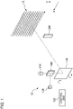
- Fig. 1 is a diagram showing a sensor device 10 according to an embodiment.
- a first direction X and a second direction Y intersect each other and are specifically orthogonal to each other.
- the first direction X is the horizontal direction.
- the positive direction of the first direction X which is the direction of the arrow indicating the first direction X, is the left direction when viewed from the movable reflection unit 120 described later toward the scanning range described later of the movable reflection unit 120.
- the negative direction of the first direction X which is the direction opposite to the direction of the arrow indicating the first direction X, is the right direction when viewed from the side where the movable reflection unit 120 is positioned toward the scanning range of the movable reflection unit 120.
- the second direction Y is the vertical direction.
- the positive direction of the second direction Y which is the direction of the arrow indicating the second direction Y, is the upward direction.
- the negative direction of the second direction Y which is the direction opposite to the direction of the arrow indicating the second direction Y, is the downward direction.
- the first direction X may be a direction different from the horizontal direction
- the second direction Y may be a direction different from the vertical direction
- the sensor device 10 includes an emitting unit 110, a movable reflection unit 120, a receiving unit 130, a beam splitter 140, and a control unit 150.
- the dotted line extending over the emitting unit 110, the movable reflection unit 120, the receiving unit 130, the beam splitter 140, and the scan line L shows electromagnetic waves propagating over the emitting unit 110, the movable reflection unit 120, the receiving unit 130, the beam splitter 140, and the scan line L.
- the electromagnetic waves reflected from the movable reflection unit 120 toward the scan line L are irradiated to the approximately central part of the region where the scan line L is formed.
- the emitting unit 110 emits electromagnetic waves such as pulsed infrared rays at regular timing intervals.
- the emitting unit 110 is an element such as a laser diode (LD) that can convert electricity such as an electric current into an electromagnetic waves such as light.
- LD laser diode
- the electromagnetic waves emitted from the emitting unit 110 pass through the beam splitter 140 and are incident on the movable reflection unit 120.
- the movable reflection unit 120 reflects the electromagnetic waves emitted from the emitting unit 110 toward a predetermined scanning range.
- the scanning range of the movable reflection unit 120 is a range that can be irradiated with the electromagnetic waves reflected by the movable reflection unit 120.
- the movable reflection unit 120 is, for example, a two-axis MEMS mirror.
- the movable reflection unit 120 is resonantly driven in the first direction X and linearly driven in the second direction Y.
- a sine wave or a cosine wave is used for the resonance drive of the movable reflection unit 120.
- a sawtooth wave or a triangular wave is used for the linear drive of the movable reflection unit 120.
- a portion of electromagnetic waves emitted from the emitting unit 110 and reflected by the movable reflection unit 120 are reflected or scattered by a target object such as an object present outside the sensor device 10.
- This electromagnetic waves return to the movable reflection unit 120, pass through the reflection by the movable reflection unit 120 and the reflection by the beam splitter 140 in order, are incident on the receiving unit 130, and are received by the receiving unit 130.
- the receiving unit 130 is an element such as an avalanche photodiode (APD) capable of converting an electromagnetic waves such as light into electricity such as an electric current.
- APD avalanche photodiode
- Another portion of electromagnetic waves emitted from the emitting unit 110 and reflected by the movable reflection unit 120 are reflected or scattered by the structure 200 positioned closer to the movable reflection unit 120 than the target object.
- This electromagnetic waves return toward the movable reflection unit 120, pass through the reflection by the movable reflection unit 120 and the transmission of the beam splitter 140 in order, are incident on the receiving unit 130, and are received by the receiving unit 130.
- the structure 200 for example, a metal or the like that has been subjected to a surface treatment having high stability over time such as plating is used.
- the distance from the movable reflection unit 120 to the structure 200 is shorter than the distance from the movable reflection unit 120 to the target object. Therefore, the time from the emitting of the electromagnetic waves from the emitting unit 110 to the receiving of the electromagnetic waves by the receiving unit 130 through the reflection of the electromagnetic waves by the structure 200 is shorter than the time from the emitting of the electromagnetic waves from the emitting unit 110 to the receiving of the electromagnetic waves by the receiving unit 130 through the reflection of the electromagnetic waves by the target object. Therefore, based on the time difference of the signal generated in the receiving unit 130, the sensor device 10 can determine whether the signal generated in the receiving unit 130 is a signal caused by the structure 200 or a signal caused by the target object.
- the sensor device 10 may include the structure 200.
- the structure 200 may be provided outside the sensor device 10.
- the structure 200 can be provided in, for example, in a window portion of a housing that houses members constituting the sensor device 10, such as the emitting unit 110, the movable reflection unit 120, the receiving unit 130, and the beam splitter 140, that is, a portion through which electromagnetic waves pass between the inside and the outside of the housing.
- the place where the structure 200 is provided is not limited to the window portion.
- control unit 150 shows blocks of functional units, not a configuration of hardware units.
- the control unit 150 is implemented by any combination of software and hardware centering on the CPU, a memory, a program loaded in the memory, a storage medium such as a hard disk for storing the program, and an interface for network connection of any computer.
- a storage medium such as a hard disk for storing the program
- an interface for network connection of any computer There are various modification examples in the implementation method and the device.
- the control unit 150 controls the amplitude of the oscillation of the movable reflection unit 120, based on the receiving result from the receiving unit 130 for the electromagnetic waves reflected or scattered by the structure 200. Further, the control unit 150 controls the interval of the emitting timing of the electromagnetic waves from the emitting unit 110, based on the receiving result from the receiving unit 130 for the electromagnetic waves reflected or scattered by the structure 200. Further, the control unit 150 shifts the emitting timing of the electromagnetic waves from the emitting unit 110, based on the receiving result from the receiving unit 130 for the electromagnetic waves reflected or scattered by the structure 200. The control unit 150 performs at least one of these controls for the emitting unit 110 and the movable reflection unit 120, according to the receiving result from the receiving unit 130 for the electromagnetic waves reflected or scattered by the structure 200. Due to the control by the control unit 150, it is possible to correct the deviation of the position of the point cloud generated by the movable reflection unit 120 from the position in the design state.
- Fig. 2 is a diagram showing an example of the relationship between the structure 200 and the scan line L of the movable reflection unit 120.
- the scan line L extends from the positive direction to the negative direction in the second direction Y, that is, the linear drive direction of the movable reflection unit 120 while turning around in the first direction X, that is, the direction of the resonance drive of the movable reflection unit 120.
- a portion of a first period T1 of the scan line L, a second period T2, and a third period T3 are shown.
- the first period T1 of the scan line L is a section from the upper end of the scan line L being at a position deviated about 1/4 period from the start point of the first period T1, through the turnaround of first stage from the top on the right side of the scan line L, to the turnaround of the first stage from above on the left side of the scan line L.
- the second period T2 of the scan line L is a section from the end point of the first period T1 of the scan line L, through the turnaround of second stage from the top on the right side of the scan line L, to the turnaround of the second stage from above on the left side of the scan line L.
- the third period T3 of the scan line L is a section from the end point of the second period T2 of the scan line L, through the turnaround of third stage from the top on the right side of the scan line L, and to the turnaround of the third stage from above on the left side of the scan line L.
- the structure 200 intersects at least a portion of a turnaround of the scan line L of the movable reflection unit 120.
- the structure 200 intersects with at least a portion of the right-side turnaround of the first period T1 of the scan line L, at least a portion of the right-side turnaround of the second period T2 of the scan line L, and at least a portion of the right-side turnaround of the third period T3 of the scan line L.
- the sensor device 10 may not be able to detect a target object in the region where the structure 200 is disposed, or may have difficulty in detecting the target object.
- the region where the sensor device 10 cannot detect the target object or has difficulty in detecting the target object can be limited to the end part of the scanning range of the movable reflection unit 120.
- the region where the structure 200 is disposed is not limited to the example shown in Fig. 2 .
- the structure 200 may be disposed approximately at or around the center in the first direction X of the region where the scan line L is generated.
- the structure 200 may be a member such as a wire extending linearly along the second direction Y. Even in this case, when the width of the structure 200 in the first direction X is relatively narrow, for example, narrower than the width of the spot generated by the movable reflection unit 120 in the first direction X, electromagnetic waves attenuated by the structure 200 can be suppressed.
- the movable reflection unit 120 In the first period T1 of the scan line L, the movable reflection unit 120 is operating in the design state. Three spots generated by the electromagnetic waves emitted from the emitting unit 110 and reflected by the movable reflection unit 120 are shown as black circles on the right-side turnaround in the first period T1 of the scan line L.
- the movable reflection unit 120 operates in a state where the gain of the transfer function of the movable reflection unit 120 deviates from the gain in the design state.
- Three spots generated by the electromagnetic waves emitted from the emitting unit 110 and reflected by the movable reflection unit 120 are shown as black circles on the right-side turnaround in the second period T2 of the scan line L. Due to the gain deviation, the amplitude of the scan line L in the first direction X in the second period T2 is smaller than the amplitude in the design state. Thus, the three spots in the second period T2 of the scan line L are deviated to the left with respect to the three spots in the first period T1 of the scan line L.
- the movable reflection unit 120 operates in a state where the phase of the transfer function of the movable reflection unit 120 deviates from the phase in the design state.
- Three spots generated by the electromagnetic waves emitted from the emitting unit 110 and reflected by the movable reflection unit 120 are shown as black circles on and near the right-side turnaround and its vicinity in the third period T3 of the scan line L. Due to the phase deviation, the phases of the three spots in the third period T3 of the scan line L is behind the phase in the design state. Thus, the three spots in the third period T3 of the scan line L deviate from the three spots in the first period T1 of the scan line L.
- Figs. 3 and 4 are diagrams for explaining a first example of control by the control unit 150.
- the field of view F such as the field of view (FOV) of the movable reflection unit 120 is shown by a broken line.
- the structure 200 shown in Figs. 1 and 2 is disposed, for example, outside the field of view F. Alternatively, the structure 200 may be disposed inside the field of view F.
- a point cloud that is, spots generated by electromagnetic waves emitted by the emitting unit 110 and reflected by the movable reflection unit 120, is shown as a plurality of black circles superimposed on the scan line L.
- the movable reflection unit 120 in the first period T1 is operating in the design state.
- the gain of the transfer function of the movable reflection unit 120 in the second period T2 deviates from the gain in the design state. Therefore, the amplitude of the scan line L in the first direction X of the second period T2 is larger than the amplitude in the design state. Therefore, in the field of view F, the point cloud of the first period T1 and the point cloud of the second period T2 are disposed so as to be offset from each other in the first direction X. Specifically, in the field of view F, the interval in the first direction X of the point cloud of the second period T2 is wider than the interval in the first direction X of the point cloud of the first period T1.
- the control unit 150 controls at least one of the amplitude of the movable reflection unit 120 and the interval of the emitting timing of the electromagnetic waves from the emitting unit 110, based on the receiving result from the receiving unit 130 for the electromagnetic waves reflected or scattered by the structure 200.
- the amplitude of the movable reflection unit 120 can be controlled by, for example, the amplitude of the drive signal input to the movable reflection unit 120.
- the control unit 150 substantially aligns the point cloud of the first period T1 and the point cloud of the second period T2 in the first direction X in the field of view F.
- the point cloud of the first period T1 and the point cloud of the second period T2 are aligned in the first direction X in the field of view F. That is, in the examples shown in Figs. 3 and 4 , the state in which the point cloud of each period in the field of view F is aligned in the first direction X as shown in Fig. 4 is a reference state such as a design state of the arrangement of the point cloud in the field of view F.
- the reference state of the arrangement of the point cloud in the field of view F is not limited to the state in which the point cloud of each period in the field of view F is aligned in the first direction X.
- the point cloud of each period in the field of view F may be deviated by a predetermined distance along the first direction X.
- the arrangement of the point cloud in the field of view F can be reverted to the arrangement in the reference state in the same manner as in the example described with reference to Figs. 3 and 4 .
- An example of controlling the amplitude of the movable reflection unit 120 by the control unit 150 is as follows.
- the control unit 150 reduces the amplitude of the oscillation of the movable reflection unit 120 in the first direction X in the second period T2 to narrow the interval in the first direction X of the point cloud in the second period T2 in the field of view F, thereby align the position of the point cloud in the first period T1 in the first direction X and the position of the point cloud in the second period T2 in the first direction X in the field of view F.
- the control unit 150 can widen the interval in the first direction X of the point cloud in the second period T2 in the field of view F, by increasing the amplitude of the oscillation of the movable reflection unit 120 in the first direction X in the second period T2, thereby align the position of the point cloud in the first period T1 in the first direction X and the position of the point cloud in the second period T2 in the first direction X in the field of view F.
- An example of controlling the interval of the emitting timing of the electromagnetic waves of the emitting unit 110 by the control unit 150 is as follows.
- the control unit 150 can narrow the interval in the first direction X of the point cloud in the second period T2 in the field of view F, by shortening the interval of the emitting timing of the electromagnetic waves from the emitting unit 110 in the field of view F.
- control unit 150 can widen the interval in the first direction X of the point cloud in the second period T2 in the field of view F, by lengthening the interval of the emitting timing of the electromagnetic waves from the emitting unit 110 in the field of view F.
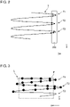
- Figs. 5 and 6 are diagrams for explaining a second example of control by the control unit 150.
- the examples shown in Figs. 5 and 6 are similar to the examples shown in Figs. 3 and 4 , except for the following points.
- the movable reflection unit 120 in the first period T1 is operating in the design state.
- the phase of the transfer function of the movable reflection unit 120 in the second period T2 deviates from the phase in the design state. Therefore, each phase of the point cloud of the second period T2 is ahead of the phase in the design state. Therefore, in the field of view F, the point cloud of the first period T1 and the point cloud of the second period T2 are disposed so as to be offset from each other in the first direction X.
- the control unit 150 shifts the emitting timing of the electromagnetic waves from the emitting unit 110, based on the receiving result from the receiving unit 130 for the electromagnetic waves reflected or scattered by the structure 200. Specifically, the control unit 150 substantially aligns the point cloud of the first period T1 and the point cloud of the second period T2 in the first direction X in the field of view F.
- the control unit 150 can align the position of the point cloud in the first period T1 in the first direction X and the position of the point cloud in the second period T2 in the first direction X in the field of view F, by accelerating the emitting timing of electromagnetic waves from the emitting unit 110 in the field of view F in the second period T2.
- control unit 150 can align the position of the point cloud in the first period T1 in the first direction X and the position of the point cloud in the second period T2 in the first direction X in the field of view F, by delaying the emitting timing of electromagnetic waves from the emitting unit 110 in the field of view F in the second period T2.
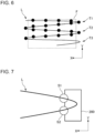
- Fig. 7 is a diagram showing a first example of a relationship between the structure 200, and a first spot S1 and a second spot S2 when the movable reflection unit 120 operates in a design state.
- Fig. 8 is a graph showing an example of a signal generated in the receiving unit 130 by the first spot S1 and the second spot S2 shown in Fig. 7 .
- Fig. 7 shows a portion of one period of the scan line L generated by the movable reflection unit 120, specifically, the right-side turnaround of the scan line L and its surroundings.
- the scan line L extends from the upper left toward the right side in Fig. 7 , turns around on the right side in Fig. 7 , and extends from the right side toward the lower left in Fig. 7 .
- the horizontal axis of the graph indicates the time t
- the vertical axis of the graph indicates the intensity of the signal generated by the receiving unit 130.
- a signal of intensity r0 is generated by the first spot S1 at time t1
- a signal of intensity r0 is generated by the second spot S2 at time t2.
- the structure 200 is provided such that the intensity r0 of the signal generated in the receiving unit 130 at time t1 by the first spot S1 when the movable reflection unit 120 operates in the design state and the intensity r0 of the signal generated in the receiving unit 130 at time t2 by the second spot S2 when the movable reflection unit 120 operates in the design state are substantially equal to each other.
- the edge of the structure 200 that intersects the right-side turnaround of the scan line L is parallel to the second direction Y.
- the reflectance of the structure 200 is uniform in any region in the structure 200.
- the intensity of the signal generated in the receiving unit 130 at time t1 by the first spot S1 when the movable reflection unit 120 operates in the design state and the intensity of the signal generated in the receiving unit 130 at time t2 by the second spot S2 when the movable reflection unit 120 operates in the design state may not be substantially equal to each other or may be different from each other.
- Fig. 9 is a diagram showing an example of a relationship between the structure 200, and the first spot S1 and the second spot S2 when the movable reflection unit 120 operates in a state where a gain in the first direction X of a transfer function of the movable reflection unit 120 deviates from the gain in the design state shown in Fig. 7 .
- Fig. 10 is a graph showing an example of a signal generated in the receiving unit 130 by the first spot S1 and the second spot S2 shown in Fig. 9 .
- the gain in the first direction X of the transfer function of the movable reflection unit 120 that is, the direction of the resonance drive, deviates from the gain in the design state.
- the amplitude of the oscillation of the movable reflection unit 120 in the first direction X is larger than the amplitude in the design state.
- the irradiation area of the first spot S1 on the structure 200 in Fig. 9 is larger than the irradiation area of the first spot S1 on the structure 200 in Fig. 7 . Therefore, the amount of electromagnetic waves received by the receiving unit 130 at time t1 in Fig. 10 is larger than the amount of electromagnetic waves received by the receiving unit 130 at time t1 in Fig. 8 . Therefore, the intensity r1 of the signal generated at time t1 in Fig. 10 is higher than the intensity r0 of the signal generated at time t1 in Fig. 8 .
- the irradiation area of the second spot S2 on the structure 200 in Fig. 9 is larger than the irradiation area of the second spot S2 on the structure 200 in Fig. 7 . Therefore, the amount of electromagnetic waves received by the receiving unit 130 at time t2 in Fig. 10 is larger than the amount of electromagnetic waves received by the receiving unit 130 at time t2 in Fig. 8 . Therefore, the intensity r1 of the signal generated at time t2 in Fig. 10 is higher than the intensity r0 of the signal generated at time t2 in Fig. 8 .
- the control unit 150 shown in Fig. 1 can determine the deviation of the gain in the first direction X of the transfer function of the movable reflection unit 120 from the gain in the design state, based on a comparison result between a relationship between a first receiving value of the electromagnetic waves reflected or scattered by a first part of the structure 200 by the receiving unit 130 and a second receiving value of the electromagnetic waves reflected or scattered by a second part of the structure 200 by the receiving unit 130 and a relationship between a first reference receiving value of the electromagnetic waves reflected or scattered by the first part of the structure 200 when the movable reflection unit 120 operates in a reference state, for example, a design state, by the receiving unit 130 and a second reference receiving value of the electromagnetic waves reflected or scattered by the second part of the structure 200 when the movable reflection unit 120 operates in the reference state by the receiving unit 130.
- a reference state for example, a design state
- the control unit 150 can perform various controls, for example, control of the amplitude of the oscillation in the first direction X of the movable reflection unit 120 or control of the interval of the emitting timing of the electromagnetic waves from the emitting unit 110.
- the first portion of the structure 200 is, for example, the portion of the structure 200 in which the first spot S1 is generated or its vicinity.
- the second portion of the structure 200 is, for example, the portion of the structure 200 in which the second spot S2 is generated or its vicinity. Further, the first portion and the second portion of the structure 200 are positioned on opposite sides of each other across the turnaround of the scan line L of the movable reflection unit 120, for example.
- the control unit 150 can determine the deviation of the gain in the first direction X of the transfer function of the movable reflection unit 120, from the gain in the design state, based on whether both the first receiving value and the second receiving value are larger or smaller than the first reference receiving value or the second reference receiving value. For example, when both the intensity r1 of the signal generated at time t1 and the intensity r1 of the signal generated at time t2 in Fig. 10 is larger than the intensity r0 of the signal generated at time t1 and the intensity r0 of the signal generated at time t2 in Fig. 8 , the control unit 150 can determine that the gain in the first direction X of the transfer function of the movable reflection unit 120 is larger than the gain in the design state.
- control unit 150 can determine that the gain in the first direction X of the transfer function of the movable reflection unit 120 is smaller than the gain in the design state.
- Fig. 11 is a diagram showing an example of a relationship between the structure 200, and the first spot S1 and the second spot S2 when the movable reflection unit 120 operates in a state where a phase of a transfer function of the movable reflection unit 120 deviates from the phase in the design state shown in Fig. 7 .
- Fig. 12 is a graph showing an example of a signal generated in the receiving unit 130 by the first spot S1 and the second spot S2 shown in Fig. 11 .
- the irradiation area of the first spot S1 on the structure 200 in Fig. 11 is larger than the irradiation area of the first spot S1 on the structure 200 in Fig. 7 . Therefore, the amount of electromagnetic waves received by the receiving unit 130 at time t1 in Fig. 12 is larger than the amount of electromagnetic waves received by the receiving unit 130 at time t1 in Fig. 8 . Therefore, the intensity r2 of the signal generated at time t1 in Fig. 12 is higher than the intensity r0 of the signal generated at time t1 in Fig. 8 .
- the irradiation area of the second spot S2 on the structure 200 in Fig. 11 is smaller than the irradiation area of the second spot S2 on the structure 200 in Fig. 7 . Therefore, the amount of electromagnetic waves received by the receiving unit 130 at time t2 in Fig. 12 is smaller than the amount of electromagnetic waves received by the receiving unit 130 at time t2 in Fig. 8 . Therefore, the intensity r3 of the signal generated at time t2 in Fig. 12 is lower than the intensity r0 of the signal generated at time t2 in Fig. 8 .
- the control unit 150 shown in Fig. 1 can determine the deviation of the phase of the transfer function of the movable reflection unit 120 from the phase of the design state, based on a comparison result between a relationship between a first receiving value of the electromagnetic waves reflected or scattered by a first part of the structure 200 by the receiving unit 130 and a second receiving value of the electromagnetic waves reflected or scattered by a second part of the structure 200 by the receiving unit 130 and a relationship between a first reference receiving value of the electromagnetic waves reflected or scattered by the first part of the structure 200 when the movable reflection unit 120 operates in a reference state, for example, a design state, by the receiving unit 130 and a second reference receiving value of the electromagnetic waves reflected or scattered by the second part of the structure 200 when the movable reflection unit 120 operates in the reference state by the receiving unit 130.
- a reference state for example, a design state
- the control unit 150 can perform various controls, for example, shift of the emitting timing of the electromagnetic waves from the emitting unit 110.
- the first portion of the structure 200 is, for example, the portion of the structure 200 in which the first spot S1 is generated or its vicinity.
- the second portion of the structure 200 is, for example, the portion of the structure 200 in which the second spot S2 is generated or its vicinity. Further, the first portion and the second portion of the structure 200 are positioned on opposite sides of each other across the turnaround of the scan line L of the movable reflection unit 120, for example.
- control unit 150 can determine the deviation of the phase of the transfer function of the movable reflection unit 120 from the phase of the design state, based on whether one of the first receiving value and the second receiving value is larger than the first reference receiving value or the second reference receiving value, and the other of the first receiving value and the second receiving value is smaller than the first reference receiving value or the second reference receiving value. For example, when the intensity r2 of the signal generated at time t1 in Fig. 12 is larger than the intensity r0 of the signal generated at time t1 in Fig. 8 , and the intensity r3 of the signal generated at time t2 in Fig. 12 is smaller than the intensity r0 of the signal generated at time t1 in Fig.
- the control unit 150 can determine that the phase of the transfer function of the movable reflection unit 120 is ahead of the phase in the design state. Further, when the intensity r2 of the signal generated at time t1 in Fig. 12 is smaller than the intensity r0 of the signal generated at time t1 in Fig. 8 , and the intensity r3 of the signal generated at time t2 in Fig. 12 is larger than the intensity r0 of the signal generated at time t1 in Fig. 8 , the control unit 150 can determine that the phase of the transfer function of the movable reflection unit 120 is behind the phase in the design state.
- Fig. 13 is a diagram showing a second example of a relationship between the structure 200A, and a first spot S1 and a second spot S2 when the movable reflection unit 120 operates in a design state.
- Fig. 14 is a graph showing an example of a signal generated in the receiving unit 130 by the first spot S1 and the second spot S2 shown in Fig. 13 .
- the structure 200A is disposed such that the intensity r0 of the signal generated in the receiving unit 130 at time t1 by the first spot S1 when the movable reflection unit 120 operates in the design state and the intensity r0' of the signal generated in the receiving unit 130 at time t2 by the second spot S2 when the movable reflection unit 120 operates in the design state are different from each other.
- the edge of the structure 200A that intersects the right-side turnaround of the scan line L is oblique to the second direction Y. More specifically, the edge of the structure 200A is inclined obliquely from the left side to the right side of the structure 200A as it goes from the upper side to the lower side of the structure 200A. Further, the reflectance of the structure 200A is uniform in any region in the structure 200A.
- Fig. 15 is a diagram showing an example of a relationship between the structure 200A, and the first spot S1 and the second spot S2 when the movable reflection unit 120 operates in a state where a gain in the second direction Y of a transfer function of the movable reflection unit 120 deviates from the gain in the design state shown in Fig. 13 .
- Fig. 16 is a graph showing an example of a signal generated in the receiving unit 130 by the first spot S1 and the second spot S2 shown in Fig. 15 .
- the gain in the second direction Y of the transfer function of the movable reflection unit 120 that is, the direction of the linear drive, deviates from the gain in the design state.
- the interval between the first spot S1 and the second spot S2 in the second direction Y is wider than the interval in the design state.
- control unit 150 can determine the deviation of the gain in the second direction Y of the transfer function of the movable reflection unit 120 from the gain in the design state, based on the comparison result of at least one of the ratio and the difference between the first receiving value and the second receiving value and at least one of the ratio and the difference between the first reference receiving value and the second reference receiving value. For example, when the ratio ⁇ is smaller than the ratio ⁇ , the control unit 150 can determine that the gain of the transfer function of the movable reflection unit 120 in the second direction Y is larger than the gain in the design state.
- the control unit 150 can determine that the gain of the transfer function of the movable reflection unit 120 in the second direction Y is smaller than the gain in the design state. Based on this determination result, the control unit 150 can perform various controls, for example, control of the amplitude of the oscillation of the movable reflection unit 120 in the second direction Y.
- the structure 200 shown in Figs. 7 and 9 and the structure 200A shown in Figs. 13 and 15 may be disposed on opposite sides in the first direction X in the region where the scan line L is formed.
- the control unit 150 can determine the deviation of the gain of the transfer function of the movable reflection unit 120 in the first direction X from the gain in the design state, by the structure 200 shown in Figs. 7 and 9 , and can determine the deviation of the gain of the transfer function of the movable reflection unit 120 in the second direction Y from the gain in the design state, by the structure 200A shown in Figs. 13 and 15 .
- the sensor device 10 is a coaxial LiDAR.
- the sensor device 10 may be a biaxial LiDAR.
- a sensor device including:
- the sensor device in which the control unit controls the amplitude of the oscillation of the movable reflection unit, based on a comparison result between a relationship between a first receiving value of the electromagnetic waves reflected or scattered by a first part of the structure by the receiving unit and a second receiving value of the electromagnetic waves reflected or scattered by a second part of the structure by the receiving unit and a relationship between a first reference receiving value of the electromagnetic waves reflected or scattered by the first part of the structure when the movable reflection unit operates in a reference state by the receiving unit and a second reference receiving value of the electromagnetic waves reflected or scattered by the second part of the structure when the movable reflection unit operates in the reference state by the receiving unit.
- the sensor device in which the control unit controls the amplitude of the oscillation of the movable reflection unit, based on whether both the first receiving value and the second receiving value are larger or smaller than the first reference receiving value or the second reference receiving value.
- the sensor device according to any one of Aspects 1-3 to 1-5, in which the first part and the second part of the structure are positioned on opposite sides of each other across a turnaround of a scan line of the movable reflection unit.
- the sensor device according to any one of Aspects 1-1 to 1-6, in which the structure intersects at least a portion of a turnaround of a scan line of the movable reflection unit.
- a sensor device including:
- the sensor device in which the control unit shifts the emitting timing of the electromagnetic waves from the emitting unit, based on a comparison result between a relationship between a first receiving value of the electromagnetic waves reflected or scattered by a first part of the structure by the receiving unit and a second receiving value of the electromagnetic waves reflected or scattered by a second part of the structure by the receiving unit and a relationship between a first reference receiving value of the electromagnetic waves reflected or scattered by the first part of the structure when the movable reflection unit operates in a reference state by the receiving unit and a second reference receiving value of the electromagnetic waves reflected or scattered by the second part of the structure when the movable reflection unit operates in the reference state by the receiving unit.
- the sensor device in which the control unit shifts the emitting timing of the electromagnetic waves from the emitting unit, based on whether or not one of the first receiving value and the second receiving value is larger than the first reference receiving value or the second reference receiving value, and the other of the first receiving value and the second receiving value is smaller than the first reference receiving value or the second reference receiving value.
- the sensor device according to Aspect 2-2 or 2-3, in which the first part and the second part of the structure are positioned on opposite sides of each other across a turnaround of a scan line of the movable reflection unit.
- the sensor device according to any one of Aspects 2-1 to 2-4, in which the structure intersects at least a portion of a turnaround of a scan line of the movable reflection unit.
Landscapes
- Physics & Mathematics (AREA)
- Engineering & Computer Science (AREA)
- General Physics & Mathematics (AREA)
- Computer Networks & Wireless Communication (AREA)
- Radar, Positioning & Navigation (AREA)
- Remote Sensing (AREA)
- Optics & Photonics (AREA)
- Electromagnetism (AREA)
- Optical Radar Systems And Details Thereof (AREA)
- Mechanical Optical Scanning Systems (AREA)
Abstract
Description
- The present invention relates to a sensor device.
- In recent years, various sensor devices, such as Light Detection And Ranging (LiDAR) have been developed. The sensor device includes a movable reflection unit such as a Micro Electro Mechanical Systems (MEMS) mirror. The sensor device reflects electromagnetic waves such as infrared rays toward a predetermined scanning range by a movable reflection unit to scan a target object such as an object present outside the sensor device.
-
Patent Document 1 describes that a reflecting member is disposed on one end side of the scanning range of the movable reflection unit in order to obtain the output direction of the laser beam reflected by the movable reflection unit. The laser beam reflected by the reflecting member is received by the light receiving unit. The distance from the movable reflection unit to the reflecting member is calculated based on the light receiving result of the light receiving unit. The direction in which the laser beam reflected by the movable reflection unit is output is calculated, based on the distance from the movable reflection unit to the reflecting member. -
Patent Document 2 describes that a reflecting member is provided in a housing accommodating a member configuring a sensor device, such as a movable reflection unit, and a deviation in the scanning position of the movable reflection unit is detected by a laser beam reflected by the reflecting member. -
- [Patent Document 1]
Japanese Unexamined Patent Publication No. 2016-6403 - [Patent Document 2]
Japanese Unexamined Patent Publication No. 2020-16481 - In the sensor device, a point cloud is generated by the irradiation of electromagnetic waves reflected by a movable reflection unit. However, the position of the point cloud may deviate from the position in the design state due to various factors, for example, the deviation of the gain of the transfer function of the movable reflection unit from the gain in the design state.
- One example of a problem to be solved by the present invention is to correct the deviation of the position of the point cloud from the position in the design state.
- The invention according to
claim 1 is a sensor device including: - a movable reflection unit that reflects electromagnetic waves toward a predetermined scanning range;
- a receiving unit that receives the electromagnetic waves reflected or scattered by a structure positioned within the scanning range; and
- a control unit that controls an amplitude of oscillation of the movable reflection unit, based on a receiving result from the receiving unit for the electromagnetic waves reflected or scattered by the structure.
-
-
Fig. 1 is a diagram showing a sensor device according to an embodiment. -
Fig. 2 is a diagram showing an example of the relationship between a structure and a scan line of a movable reflection unit. -
Fig. 3 is a diagram for explaining a first example of control by a control unit. -
Fig. 4 is a diagram for explaining a first example of control by the control unit. -
Fig. 5 is a diagram for explaining a second example of control by the control unit. -
Fig. 6 is a diagram for explaining a second example of control by the control unit. -
Fig. 7 is a diagram showing a first example of a relationship between the structure, and a first spot and a second spot when the movable reflection unit operates in a design state. -
Fig. 8 is a graph showing an example of a signal generated in a receiving unit by the first spot and the second spot shown inFig. 7 . -
Fig. 9 is a diagram showing an example of a relationship between the structure, and a first spot and a second spot when the movable reflection unit operates in a state where a gain in a first direction of a transfer function of the movable reflection unit deviates from the gain in the design state shown inFig. 7 . -
Fig. 10 is a graph showing an example of a signal generated in the receiving unit by the first spot and the second spot shown inFig. 9 . -
Fig. 11 is a diagram showing an example of a relationship between the structure, and a first spot and a second spot when the movable reflection unit operates in a state where a phase of a transfer function of the movable reflection unit deviates from the phase in the design state shown inFig. 7 . -
Fig. 12 is a graph showing an example of a signal generated in the receiving unit by the first spot and the second spot shown inFig. 11 . -
Fig. 13 is a diagram showing a second example of a relationship between the structure, and a first spot and a second spot when the movable reflection unit operates in a design state. -
Fig. 14 is a graph showing an example of a signal generated in the receiving unit by the first spot and the second spot shown inFig. 13 . -
Fig. 15 is a diagram showing an example of a relationship between the structure, and a first spot and a second spot when the movable reflection unit operates in a state where a gain in a second direction of a transfer function of the movable reflection unit deviates from the gain in the design state shown inFig. 13 . -
Fig. 16 is a graph showing an example of a signal generated in the receiving unit by the first spot and the second spot shown inFig. 15 . - Hereinafter, embodiments of the present invention will be described with reference to the drawings. In all drawings, similar components are designated by the same reference numerals, and description thereof will not be repeated as appropriate.
-
Fig. 1 is a diagram showing asensor device 10 according to an embodiment. - In
Fig. 1 , a first direction X and a second direction Y intersect each other and are specifically orthogonal to each other. InFig. 1 , the first direction X is the horizontal direction. The positive direction of the first direction X, which is the direction of the arrow indicating the first direction X, is the left direction when viewed from themovable reflection unit 120 described later toward the scanning range described later of themovable reflection unit 120. The negative direction of the first direction X, which is the direction opposite to the direction of the arrow indicating the first direction X, is the right direction when viewed from the side where themovable reflection unit 120 is positioned toward the scanning range of themovable reflection unit 120. The second direction Y is the vertical direction. The positive direction of the second direction Y, which is the direction of the arrow indicating the second direction Y, is the upward direction. The negative direction of the second direction Y, which is the direction opposite to the direction of the arrow indicating the second direction Y, is the downward direction. - As is clear from the description of the present specification, the first direction X may be a direction different from the horizontal direction, and the second direction Y may be a direction different from the vertical direction.
- The
sensor device 10 includes anemitting unit 110, amovable reflection unit 120, areceiving unit 130, abeam splitter 140, and acontrol unit 150. InFig. 1 , the dotted line extending over theemitting unit 110, themovable reflection unit 120, thereceiving unit 130, thebeam splitter 140, and the scan line L shows electromagnetic waves propagating over theemitting unit 110, themovable reflection unit 120, thereceiving unit 130, thebeam splitter 140, and the scan line L. InFig. 1 , the electromagnetic waves reflected from themovable reflection unit 120 toward the scan line L are irradiated to the approximately central part of the region where the scan line L is formed. - The emitting
unit 110 emits electromagnetic waves such as pulsed infrared rays at regular timing intervals. Theemitting unit 110 is an element such as a laser diode (LD) that can convert electricity such as an electric current into an electromagnetic waves such as light. The electromagnetic waves emitted from the emittingunit 110 pass through thebeam splitter 140 and are incident on themovable reflection unit 120. - The
movable reflection unit 120 reflects the electromagnetic waves emitted from the emittingunit 110 toward a predetermined scanning range. The scanning range of themovable reflection unit 120 is a range that can be irradiated with the electromagnetic waves reflected by themovable reflection unit 120. Themovable reflection unit 120 is, for example, a two-axis MEMS mirror. Themovable reflection unit 120 is resonantly driven in the first direction X and linearly driven in the second direction Y. For example, a sine wave or a cosine wave is used for the resonance drive of themovable reflection unit 120. For example, a sawtooth wave or a triangular wave is used for the linear drive of themovable reflection unit 120. - A portion of electromagnetic waves emitted from the
emitting unit 110 and reflected by themovable reflection unit 120 are reflected or scattered by a target object such as an object present outside thesensor device 10. This electromagnetic waves return to themovable reflection unit 120, pass through the reflection by themovable reflection unit 120 and the reflection by thebeam splitter 140 in order, are incident on thereceiving unit 130, and are received by thereceiving unit 130. The receivingunit 130 is an element such as an avalanche photodiode (APD) capable of converting an electromagnetic waves such as light into electricity such as an electric current. - Another portion of electromagnetic waves emitted from the emitting
unit 110 and reflected by themovable reflection unit 120 are reflected or scattered by thestructure 200 positioned closer to themovable reflection unit 120 than the target object. This electromagnetic waves return toward themovable reflection unit 120, pass through the reflection by themovable reflection unit 120 and the transmission of thebeam splitter 140 in order, are incident on the receivingunit 130, and are received by the receivingunit 130. As thestructure 200, for example, a metal or the like that has been subjected to a surface treatment having high stability over time such as plating is used. - The distance from the
movable reflection unit 120 to thestructure 200 is shorter than the distance from themovable reflection unit 120 to the target object. Therefore, the time from the emitting of the electromagnetic waves from the emittingunit 110 to the receiving of the electromagnetic waves by the receivingunit 130 through the reflection of the electromagnetic waves by thestructure 200 is shorter than the time from the emitting of the electromagnetic waves from the emittingunit 110 to the receiving of the electromagnetic waves by the receivingunit 130 through the reflection of the electromagnetic waves by the target object. Therefore, based on the time difference of the signal generated in the receivingunit 130, thesensor device 10 can determine whether the signal generated in the receivingunit 130 is a signal caused by thestructure 200 or a signal caused by the target object. - The
sensor device 10 may include thestructure 200. Alternatively, thestructure 200 may be provided outside thesensor device 10. When thesensor device 10 includes thestructure 200, thestructure 200 can be provided in, for example, in a window portion of a housing that houses members constituting thesensor device 10, such as the emittingunit 110, themovable reflection unit 120, the receivingunit 130, and thebeam splitter 140, that is, a portion through which electromagnetic waves pass between the inside and the outside of the housing. However, the place where thestructure 200 is provided is not limited to the window portion. - In the present embodiment, the
control unit 150 shows blocks of functional units, not a configuration of hardware units. Thecontrol unit 150 is implemented by any combination of software and hardware centering on the CPU, a memory, a program loaded in the memory, a storage medium such as a hard disk for storing the program, and an interface for network connection of any computer. There are various modification examples in the implementation method and the device. - The
control unit 150 controls the amplitude of the oscillation of themovable reflection unit 120, based on the receiving result from the receivingunit 130 for the electromagnetic waves reflected or scattered by thestructure 200. Further, thecontrol unit 150 controls the interval of the emitting timing of the electromagnetic waves from the emittingunit 110, based on the receiving result from the receivingunit 130 for the electromagnetic waves reflected or scattered by thestructure 200. Further, thecontrol unit 150 shifts the emitting timing of the electromagnetic waves from the emittingunit 110, based on the receiving result from the receivingunit 130 for the electromagnetic waves reflected or scattered by thestructure 200. Thecontrol unit 150 performs at least one of these controls for the emittingunit 110 and themovable reflection unit 120, according to the receiving result from the receivingunit 130 for the electromagnetic waves reflected or scattered by thestructure 200. Due to the control by thecontrol unit 150, it is possible to correct the deviation of the position of the point cloud generated by themovable reflection unit 120 from the position in the design state. -
Fig. 2 is a diagram showing an example of the relationship between thestructure 200 and the scan line L of themovable reflection unit 120. - The scan line L extends from the positive direction to the negative direction in the second direction Y, that is, the linear drive direction of the
movable reflection unit 120 while turning around in the first direction X, that is, the direction of the resonance drive of themovable reflection unit 120. InFig. 2 , a portion of a first period T1 of the scan line L, a second period T2, and a third period T3 are shown. - The first period T1 of the scan line L is a section from the upper end of the scan line L being at a position deviated about 1/4 period from the start point of the first period T1, through the turnaround of first stage from the top on the right side of the scan line L, to the turnaround of the first stage from above on the left side of the scan line L.
- The second period T2 of the scan line L is a section from the end point of the first period T1 of the scan line L, through the turnaround of second stage from the top on the right side of the scan line L, to the turnaround of the second stage from above on the left side of the scan line L.
- The third period T3 of the scan line L is a section from the end point of the second period T2 of the scan line L, through the turnaround of third stage from the top on the right side of the scan line L, and to the turnaround of the third stage from above on the left side of the scan line L.
- The
structure 200 intersects at least a portion of a turnaround of the scan line L of themovable reflection unit 120. In the example shown inFig. 2 , thestructure 200 intersects with at least a portion of the right-side turnaround of the first period T1 of the scan line L, at least a portion of the right-side turnaround of the second period T2 of the scan line L, and at least a portion of the right-side turnaround of the third period T3 of the scan line L. When thestructure 200 is disposed approximately at or around the center in the first direction X of the region where the scan line L is generated, thesensor device 10 may not be able to detect a target object in the region where thestructure 200 is disposed, or may have difficulty in detecting the target object. On the other hand, in the present embodiment, the region where thesensor device 10 cannot detect the target object or has difficulty in detecting the target object can be limited to the end part of the scanning range of themovable reflection unit 120. - The region where the
structure 200 is disposed is not limited to the example shown inFig. 2 . For example, thestructure 200 may be disposed approximately at or around the center in the first direction X of the region where the scan line L is generated. For example, thestructure 200 may be a member such as a wire extending linearly along the second direction Y. Even in this case, when the width of thestructure 200 in the first direction X is relatively narrow, for example, narrower than the width of the spot generated by themovable reflection unit 120 in the first direction X, electromagnetic waves attenuated by thestructure 200 can be suppressed. - In the first period T1 of the scan line L, the
movable reflection unit 120 is operating in the design state. Three spots generated by the electromagnetic waves emitted from the emittingunit 110 and reflected by themovable reflection unit 120 are shown as black circles on the right-side turnaround in the first period T1 of the scan line L. - In the second period T2 of the scan line L, the
movable reflection unit 120 operates in a state where the gain of the transfer function of themovable reflection unit 120 deviates from the gain in the design state. Three spots generated by the electromagnetic waves emitted from the emittingunit 110 and reflected by themovable reflection unit 120 are shown as black circles on the right-side turnaround in the second period T2 of the scan line L. Due to the gain deviation, the amplitude of the scan line L in the first direction X in the second period T2 is smaller than the amplitude in the design state. Thus, the three spots in the second period T2 of the scan line L are deviated to the left with respect to the three spots in the first period T1 of the scan line L. - In the third period T3 of the scan line L, the
movable reflection unit 120 operates in a state where the phase of the transfer function of themovable reflection unit 120 deviates from the phase in the design state. Three spots generated by the electromagnetic waves emitted from the emittingunit 110 and reflected by themovable reflection unit 120 are shown as black circles on and near the right-side turnaround and its vicinity in the third period T3 of the scan line L. Due to the phase deviation, the phases of the three spots in the third period T3 of the scan line L is behind the phase in the design state. Thus, the three spots in the third period T3 of the scan line L deviate from the three spots in the first period T1 of the scan line L. -
Figs. 3 and4 are diagrams for explaining a first example of control by thecontrol unit 150. - In
Figs. 3 and4 , the field of view F such as the field of view (FOV) of themovable reflection unit 120 is shown by a broken line. Thestructure 200 shown inFigs. 1 and2 is disposed, for example, outside the field of view F. Alternatively, thestructure 200 may be disposed inside the field of view F. - In
Figs. 3 and4 , a point cloud, that is, spots generated by electromagnetic waves emitted by the emittingunit 110 and reflected by themovable reflection unit 120, is shown as a plurality of black circles superimposed on the scan line L. - In
Fig. 3 , themovable reflection unit 120 in the first period T1 is operating in the design state. In contrast, the gain of the transfer function of themovable reflection unit 120 in the second period T2 deviates from the gain in the design state. Therefore, the amplitude of the scan line L in the first direction X of the second period T2 is larger than the amplitude in the design state. Therefore, in the field of view F, the point cloud of the first period T1 and the point cloud of the second period T2 are disposed so as to be offset from each other in the first direction X. Specifically, in the field of view F, the interval in the first direction X of the point cloud of the second period T2 is wider than the interval in the first direction X of the point cloud of the first period T1. - In
Fig. 4 , thecontrol unit 150 controls at least one of the amplitude of themovable reflection unit 120 and the interval of the emitting timing of the electromagnetic waves from the emittingunit 110, based on the receiving result from the receivingunit 130 for the electromagnetic waves reflected or scattered by thestructure 200. The amplitude of themovable reflection unit 120 can be controlled by, for example, the amplitude of the drive signal input to themovable reflection unit 120. Specifically, thecontrol unit 150 substantially aligns the point cloud of the first period T1 and the point cloud of the second period T2 in the first direction X in the field of view F. - In the examples shown in
Figs. 3 and4 , it is described that the point cloud of the first period T1 and the point cloud of the second period T2 are aligned in the first direction X in the field of view F. That is, in the examples shown inFigs. 3 and4 , the state in which the point cloud of each period in the field of view F is aligned in the first direction X as shown inFig. 4 is a reference state such as a design state of the arrangement of the point cloud in the field of view F. However, the reference state of the arrangement of the point cloud in the field of view F is not limited to the state in which the point cloud of each period in the field of view F is aligned in the first direction X. For example, in the reference state of the arrangement of the point cloud in the field of view F, the point cloud of each period in the field of view F may be deviated by a predetermined distance along the first direction X. Even in this example, even when the arrangement of the point cloud in the field of view F deviates from the arrangement in the reference state, the arrangement of the point cloud in the field of view F can be reverted to the arrangement in the reference state in the same manner as in the example described with reference toFigs. 3 and4 . The same applies toFigs. 5 and6 described later. - An example of controlling the amplitude of the
movable reflection unit 120 by thecontrol unit 150 is as follows. - For example, as shown in
Fig. 3 , when the interval in the first direction X of the point cloud in the second period T2 is wider than the interval in the first direction X of the point cloud in the first period T1 in the field of view F, the control unit 150 reduces the amplitude of the oscillation of the movable reflection unit 120 in the first direction X in the second period T2 to narrow the interval in the first direction X of the point cloud in the second period T2 in the field of view F, thereby align the position of the point cloud in the first period T1 in the first direction X and the position of the point cloud in the second period T2 in the first direction X in the field of view F. Further, when the interval in the first direction X of the point cloud in the second period T2 is narrower than the interval in the first direction X of the point cloud in the first period T1 in the field of view F, the control unit 150 can widen the interval in the first direction X of the point cloud in the second period T2 in the field of view F, by increasing the amplitude of the oscillation of the movable reflection unit 120 in the first direction X in the second period T2, thereby align the position of the point cloud in the first period T1 in the first direction X and the position of the point cloud in the second period T2 in the first direction X in the field of view F. - An example of controlling the interval of the emitting timing of the electromagnetic waves of the emitting
unit 110 by thecontrol unit 150 is as follows. - For example, as shown in
Fig. 3 , when the interval in the first direction X of the point cloud in the second period T2 is wider than the interval in the first direction X of the point cloud in the first period T1 in the field of view F, thecontrol unit 150 can narrow the interval in the first direction X of the point cloud in the second period T2 in the field of view F, by shortening the interval of the emitting timing of the electromagnetic waves from the emittingunit 110 in the field of view F. Further, when the interval in the first direction X of the point cloud in the second period T2 is narrower than the interval in the first direction X of the point cloud in the first period T1 in the field of view F, thecontrol unit 150 can widen the interval in the first direction X of the point cloud in the second period T2 in the field of view F, by lengthening the interval of the emitting timing of the electromagnetic waves from the emittingunit 110 in the field of view F. -
Figs. 5 and6 are diagrams for explaining a second example of control by thecontrol unit 150. The examples shown inFigs. 5 and6 are similar to the examples shown inFigs. 3 and4 , except for the following points. - In
Fig. 5 , themovable reflection unit 120 in the first period T1 is operating in the design state. In contrast, the phase of the transfer function of themovable reflection unit 120 in the second period T2 deviates from the phase in the design state. Therefore, each phase of the point cloud of the second period T2 is ahead of the phase in the design state. Therefore, in the field of view F, the point cloud of the first period T1 and the point cloud of the second period T2 are disposed so as to be offset from each other in the first direction X. - In
Fig. 6 , thecontrol unit 150 shifts the emitting timing of the electromagnetic waves from the emittingunit 110, based on the receiving result from the receivingunit 130 for the electromagnetic waves reflected or scattered by thestructure 200. Specifically, thecontrol unit 150 substantially aligns the point cloud of the first period T1 and the point cloud of the second period T2 in the first direction X in the field of view F. - An example of the shift of the emitting timing of the electromagnetic waves from the emitting
unit 110 by thecontrol unit 150 is as follows. - For example, as shown in
Fig. 5 , when each phase of the point cloud in the second period T2 is ahead of the phase in the design state, thecontrol unit 150 can align the position of the point cloud in the first period T1 in the first direction X and the position of the point cloud in the second period T2 in the first direction X in the field of view F, by accelerating the emitting timing of electromagnetic waves from the emittingunit 110 in the field of view F in the second period T2. Further, when each phase of the point cloud in the second period T2 is behind the phase in the design state, thecontrol unit 150 can align the position of the point cloud in the first period T1 in the first direction X and the position of the point cloud in the second period T2 in the first direction X in the field of view F, by delaying the emitting timing of electromagnetic waves from the emittingunit 110 in the field of view F in the second period T2. -
Fig. 7 is a diagram showing a first example of a relationship between thestructure 200, and a first spot S1 and a second spot S2 when themovable reflection unit 120 operates in a design state.Fig. 8 is a graph showing an example of a signal generated in the receivingunit 130 by the first spot S1 and the second spot S2 shown inFig. 7 . -
Fig. 7 shows a portion of one period of the scan line L generated by themovable reflection unit 120, specifically, the right-side turnaround of the scan line L and its surroundings. The scan line L extends from the upper left toward the right side inFig. 7 , turns around on the right side inFig. 7 , and extends from the right side toward the lower left inFig. 7 . - In
Fig. 8 , the horizontal axis of the graph indicates the time t, and the vertical axis of the graph indicates the intensity of the signal generated by the receivingunit 130. InFig. 8 , a signal of intensity r0 is generated by the first spot S1 at time t1, and a signal of intensity r0 is generated by the second spot S2 at time t2. - In
Figs. 7 and8 , thestructure 200 is provided such that the intensity r0 of the signal generated in the receivingunit 130 at time t1 by the first spot S1 when themovable reflection unit 120 operates in the design state and the intensity r0 of the signal generated in the receivingunit 130 at time t2 by the second spot S2 when themovable reflection unit 120 operates in the design state are substantially equal to each other. Specifically, the edge of thestructure 200 that intersects the right-side turnaround of the scan line L is parallel to the second direction Y. Further, the reflectance of thestructure 200 is uniform in any region in thestructure 200. However, the intensity of the signal generated in the receivingunit 130 at time t1 by the first spot S1 when themovable reflection unit 120 operates in the design state and the intensity of the signal generated in the receivingunit 130 at time t2 by the second spot S2 when themovable reflection unit 120 operates in the design state may not be substantially equal to each other or may be different from each other. -
Fig. 9 is a diagram showing an example of a relationship between thestructure 200, and the first spot S1 and the second spot S2 when themovable reflection unit 120 operates in a state where a gain in the first direction X of a transfer function of themovable reflection unit 120 deviates from the gain in the design state shown inFig. 7 .Fig. 10 is a graph showing an example of a signal generated in the receivingunit 130 by the first spot S1 and the second spot S2 shown inFig. 9 . - In
Fig. 9 , the gain in the first direction X of the transfer function of themovable reflection unit 120, that is, the direction of the resonance drive, deviates from the gain in the design state. Thus, the amplitude of the oscillation of themovable reflection unit 120 in the first direction X is larger than the amplitude in the design state. - The irradiation area of the first spot S1 on the
structure 200 inFig. 9 is larger than the irradiation area of the first spot S1 on thestructure 200 inFig. 7 . Therefore, the amount of electromagnetic waves received by the receivingunit 130 at time t1 inFig. 10 is larger than the amount of electromagnetic waves received by the receivingunit 130 at time t1 inFig. 8 . Therefore, the intensity r1 of the signal generated at time t1 inFig. 10 is higher than the intensity r0 of the signal generated at time t1 inFig. 8 . - The irradiation area of the second spot S2 on the
structure 200 inFig. 9 is larger than the irradiation area of the second spot S2 on thestructure 200 inFig. 7 . Therefore, the amount of electromagnetic waves received by the receivingunit 130 at time t2 inFig. 10 is larger than the amount of electromagnetic waves received by the receivingunit 130 at time t2 inFig. 8 . Therefore, the intensity r1 of the signal generated at time t2 inFig. 10 is higher than the intensity r0 of the signal generated at time t2 inFig. 8 . - The
control unit 150 shown inFig. 1 can determine the deviation of the gain in the first direction X of the transfer function of themovable reflection unit 120 from the gain in the design state, based on a comparison result between a relationship between a first receiving value of the electromagnetic waves reflected or scattered by a first part of thestructure 200 by the receivingunit 130 and a second receiving value of the electromagnetic waves reflected or scattered by a second part of thestructure 200 by the receivingunit 130 and a relationship between a first reference receiving value of the electromagnetic waves reflected or scattered by the first part of thestructure 200 when themovable reflection unit 120 operates in a reference state, for example, a design state, by the receivingunit 130 and a second reference receiving value of the electromagnetic waves reflected or scattered by the second part of thestructure 200 when themovable reflection unit 120 operates in the reference state by the receivingunit 130. Based on this determination result, thecontrol unit 150 can perform various controls, for example, control of the amplitude of the oscillation in the first direction X of themovable reflection unit 120 or control of the interval of the emitting timing of the electromagnetic waves from the emittingunit 110. The first portion of thestructure 200 is, for example, the portion of thestructure 200 in which the first spot S1 is generated or its vicinity. The second portion of thestructure 200 is, for example, the portion of thestructure 200 in which the second spot S2 is generated or its vicinity. Further, the first portion and the second portion of thestructure 200 are positioned on opposite sides of each other across the turnaround of the scan line L of themovable reflection unit 120, for example. - For example, the
control unit 150 can determine the deviation of the gain in the first direction X of the transfer function of themovable reflection unit 120, from the gain in the design state, based on whether both the first receiving value and the second receiving value are larger or smaller than the first reference receiving value or the second reference receiving value. For example, when both the intensity r1 of the signal generated at time t1 and the intensity r1 of the signal generated at time t2 inFig. 10 is larger than the intensity r0 of the signal generated at time t1 and the intensity r0 of the signal generated at time t2 inFig. 8 , thecontrol unit 150 can determine that the gain in the first direction X of the transfer function of themovable reflection unit 120 is larger than the gain in the design state. Further, when both the intensity r1 of the signal generated at time t1 and the intensity r1 of the signal generated at time t2 inFig. 10 is smaller than the intensity r0 of the signal generated at time t1 and the intensity r0 of the signal generated at time t2 inFig. 8 , thecontrol unit 150 can determine that the gain in the first direction X of the transfer function of themovable reflection unit 120 is smaller than the gain in the design state. -
Fig. 11 is a diagram showing an example of a relationship between thestructure 200, and the first spot S1 and the second spot S2 when themovable reflection unit 120 operates in a state where a phase of a transfer function of themovable reflection unit 120 deviates from the phase in the design state shown inFig. 7 .Fig. 12 is a graph showing an example of a signal generated in the receivingunit 130 by the first spot S1 and the second spot S2 shown inFig. 11 . - In
Fig. 11 , the phase of the transfer function of themovable reflection unit 120 is ahead of the phase in the design state. - The irradiation area of the first spot S1 on the
structure 200 inFig. 11 is larger than the irradiation area of the first spot S1 on thestructure 200 inFig. 7 . Therefore, the amount of electromagnetic waves received by the receivingunit 130 at time t1 inFig. 12 is larger than the amount of electromagnetic waves received by the receivingunit 130 at time t1 inFig. 8 . Therefore, the intensity r2 of the signal generated at time t1 inFig. 12 is higher than the intensity r0 of the signal generated at time t1 inFig. 8 . - The irradiation area of the second spot S2 on the
structure 200 inFig. 11 is smaller than the irradiation area of the second spot S2 on thestructure 200 inFig. 7 . Therefore, the amount of electromagnetic waves received by the receivingunit 130 at time t2 inFig. 12 is smaller than the amount of electromagnetic waves received by the receivingunit 130 at time t2 inFig. 8 . Therefore, the intensity r3 of the signal generated at time t2 inFig. 12 is lower than the intensity r0 of the signal generated at time t2 inFig. 8 . - The
control unit 150 shown inFig. 1 can determine the deviation of the phase of the transfer function of themovable reflection unit 120 from the phase of the design state, based on a comparison result between a relationship between a first receiving value of the electromagnetic waves reflected or scattered by a first part of thestructure 200 by the receivingunit 130 and a second receiving value of the electromagnetic waves reflected or scattered by a second part of thestructure 200 by the receivingunit 130 and a relationship between a first reference receiving value of the electromagnetic waves reflected or scattered by the first part of thestructure 200 when themovable reflection unit 120 operates in a reference state, for example, a design state, by the receivingunit 130 and a second reference receiving value of the electromagnetic waves reflected or scattered by the second part of thestructure 200 when themovable reflection unit 120 operates in the reference state by the receivingunit 130. Based on this determination result, thecontrol unit 150 can perform various controls, for example, shift of the emitting timing of the electromagnetic waves from the emittingunit 110. The first portion of thestructure 200 is, for example, the portion of thestructure 200 in which the first spot S1 is generated or its vicinity. The second portion of thestructure 200 is, for example, the portion of thestructure 200 in which the second spot S2 is generated or its vicinity. Further, the first portion and the second portion of thestructure 200 are positioned on opposite sides of each other across the turnaround of the scan line L of themovable reflection unit 120, for example. - For example, the
control unit 150 can determine the deviation of the phase of the transfer function of themovable reflection unit 120 from the phase of the design state, based on whether one of the first receiving value and the second receiving value is larger than the first reference receiving value or the second reference receiving value, and the other of the first receiving value and the second receiving value is smaller than the first reference receiving value or the second reference receiving value. For example, when the intensity r2 of the signal generated at time t1 inFig. 12 is larger than the intensity r0 of the signal generated at time t1 inFig. 8 , and the intensity r3 of the signal generated at time t2 inFig. 12 is smaller than the intensity r0 of the signal generated at time t1 inFig. 8 , thecontrol unit 150 can determine that the phase of the transfer function of themovable reflection unit 120 is ahead of the phase in the design state. Further, when the intensity r2 of the signal generated at time t1 inFig. 12 is smaller than the intensity r0 of the signal generated at time t1 inFig. 8 , and the intensity r3 of the signal generated at time t2 inFig. 12 is larger than the intensity r0 of the signal generated at time t1 inFig. 8 , thecontrol unit 150 can determine that the phase of the transfer function of themovable reflection unit 120 is behind the phase in the design state. -
Fig. 13 is a diagram showing a second example of a relationship between thestructure 200A, and a first spot S1 and a second spot S2 when themovable reflection unit 120 operates in a design state.Fig. 14 is a graph showing an example of a signal generated in the receivingunit 130 by the first spot S1 and the second spot S2 shown inFig. 13 . - In
Figs. 13 and14 , thestructure 200A is disposed such that the intensity r0 of the signal generated in the receivingunit 130 at time t1 by the first spot S1 when themovable reflection unit 120 operates in the design state and the intensity r0' of the signal generated in the receivingunit 130 at time t2 by the second spot S2 when themovable reflection unit 120 operates in the design state are different from each other. Specifically, the edge of thestructure 200A that intersects the right-side turnaround of the scan line L is oblique to the second direction Y. More specifically, the edge of thestructure 200A is inclined obliquely from the left side to the right side of thestructure 200A as it goes from the upper side to the lower side of thestructure 200A. Further, the reflectance of thestructure 200A is uniform in any region in thestructure 200A. -
Fig. 15 is a diagram showing an example of a relationship between thestructure 200A, and the first spot S1 and the second spot S2 when themovable reflection unit 120 operates in a state where a gain in the second direction Y of a transfer function of themovable reflection unit 120 deviates from the gain in the design state shown inFig. 13 .Fig. 16 is a graph showing an example of a signal generated in the receivingunit 130 by the first spot S1 and the second spot S2 shown inFig. 15 . - In
Fig. 15 , the gain in the second direction Y of the transfer function of themovable reflection unit 120, that is, the direction of the linear drive, deviates from the gain in the design state. Thus, the interval between the first spot S1 and the second spot S2 in the second direction Y is wider than the interval in the design state. - The ratio of the irradiation area of the second spot S2 on the
structure 200A with respect to the irradiation area of the first spot S1 on thestructure 200A inFig. 15 is smaller than the ratio of the irradiation area of the second spot S2 on thestructure 200A with respect to the irradiation area of the first spot S1 on thestructure 200A inFig. 13 . Therefore, the ratio β of the intensity r1' of the signal generated at time t2 with respect to the intensity r1 of the signal generated at time t1 inFig. 16 is smaller than the ratio α of the intensity r0' of the signal generated at time t2 with respect to the intensity r0 of the signal generated at time t1 inFig. 14 (α = r0'/r0, β = r1'/r1). - For example, the
control unit 150 can determine the deviation of the gain in the second direction Y of the transfer function of themovable reflection unit 120 from the gain in the design state, based on the comparison result of at least one of the ratio and the difference between the first receiving value and the second receiving value and at least one of the ratio and the difference between the first reference receiving value and the second reference receiving value. For example, when the ratio β is smaller than the ratio α, thecontrol unit 150 can determine that the gain of the transfer function of themovable reflection unit 120 in the second direction Y is larger than the gain in the design state. Further, when the ratio β is larger than the ratio α, thecontrol unit 150 can determine that the gain of the transfer function of themovable reflection unit 120 in the second direction Y is smaller than the gain in the design state. Based on this determination result, thecontrol unit 150 can perform various controls, for example, control of the amplitude of the oscillation of themovable reflection unit 120 in the second direction Y. - The
structure 200 shown inFigs. 7 and9 and thestructure 200A shown inFigs. 13 and15 may be disposed on opposite sides in the first direction X in the region where the scan line L is formed. In this case, thecontrol unit 150 can determine the deviation of the gain of the transfer function of themovable reflection unit 120 in the first direction X from the gain in the design state, by thestructure 200 shown inFigs. 7 and9 , and can determine the deviation of the gain of the transfer function of themovable reflection unit 120 in the second direction Y from the gain in the design state, by thestructure 200A shown inFigs. 13 and15 . - Although the embodiment has been described above with reference to the drawings, these are examples of the present invention, and various configurations other than the above can be adopted.
- For example, in the embodiment, the
sensor device 10 is a coaxial LiDAR. However, thesensor device 10 may be a biaxial LiDAR. - According to the present specification, the following aspects are provided.
- A sensor device including:
- a movable reflection unit that reflects electromagnetic waves toward a predetermined scanning range;
- a receiving unit that receives the electromagnetic waves reflected or scattered by a structure positioned within the scanning range; and
- a control unit that controls an amplitude of oscillation of the movable reflection unit, based on a receiving result from the receiving unit for the electromagnetic waves reflected or scattered by the structure.
- The sensor device according to Aspect 1-1, in which
- the movable reflection unit reflects the electromagnetic waves emitted from an emitting unit toward the scanning range, and
- the control unit further controls an interval of an emitting timing of the electromagnetic waves from the emitting unit.
- The sensor device according to Aspect 1-1 or 1-2, in which
the control unit controls the amplitude of the oscillation of the movable reflection unit, based on a comparison result between a relationship between a first receiving value of the electromagnetic waves reflected or scattered by a first part of the structure by the receiving unit and a second receiving value of the electromagnetic waves reflected or scattered by a second part of the structure by the receiving unit and a relationship between a first reference receiving value of the electromagnetic waves reflected or scattered by the first part of the structure when the movable reflection unit operates in a reference state by the receiving unit and a second reference receiving value of the electromagnetic waves reflected or scattered by the second part of the structure when the movable reflection unit operates in the reference state by the receiving unit. - The sensor device according to Aspect 1-3, in which
the control unit controls the amplitude of the oscillation of the movable reflection unit, based on whether both the first receiving value and the second receiving value are larger or smaller than the first reference receiving value or the second reference receiving value. - The sensor device according to Aspect 1-3, in which
- the structure is provided such that the first reference receiving value and the second reference receiving value are different from each other, and
- the control unit controls the amplitude of the oscillation of the movable reflection unit, based on a comparison result between at least one of a ratio and a difference between the first receiving value and the second receiving value and at least one of a ratio and a difference between the first reference receiving value and the second reference receiving value.
- The sensor device according to any one of Aspects 1-3 to 1-5, in which
the first part and the second part of the structure are positioned on opposite sides of each other across a turnaround of a scan line of the movable reflection unit. - The sensor device according to any one of Aspects 1-1 to 1-6, in which
the structure intersects at least a portion of a turnaround of a scan line of the movable reflection unit. - A sensor device including:
- an emitting unit that emits electromagnetic waves;
- a movable reflection unit that reflects the electromagnetic waves toward a predetermined scanning range;
- a receiving unit that receives the electromagnetic waves reflected or scattered by a structure positioned within the scanning range; and
- a control unit that shifts an emitting timing of the electromagnetic waves from the emitting unit, based on a receiving result from the receiving unit for the electromagnetic waves reflected by the structure.
- The sensor device according to Aspect 2-1, in which
the control unit shifts the emitting timing of the electromagnetic waves from the emitting unit, based on a comparison result between a relationship between a first receiving value of the electromagnetic waves reflected or scattered by a first part of the structure by the receiving unit and a second receiving value of the electromagnetic waves reflected or scattered by a second part of the structure by the receiving unit and a relationship between a first reference receiving value of the electromagnetic waves reflected or scattered by the first part of the structure when the movable reflection unit operates in a reference state by the receiving unit and a second reference receiving value of the electromagnetic waves reflected or scattered by the second part of the structure when the movable reflection unit operates in the reference state by the receiving unit. - The sensor device according to Aspect 2-2, in which
the control unit shifts the emitting timing of the electromagnetic waves from the emitting unit, based on whether or not one of the first receiving value and the second receiving value is larger than the first reference receiving value or the second reference receiving value, and the other of the first receiving value and the second receiving value is smaller than the first reference receiving value or the second reference receiving value. - The sensor device according to Aspect 2-2 or 2-3, in which
the first part and the second part of the structure are positioned on opposite sides of each other across a turnaround of a scan line of the movable reflection unit. - The sensor device according to any one of Aspects 2-1 to 2-4, in which
the structure intersects at least a portion of a turnaround of a scan line of the movable reflection unit. - This application is based upon and claims the benefit of priority from
Japanese Patent Application No. 2020-058896, filed March 27, 2020 -
- 10 sensor device
110 emitting unit - 120 movable reflection unit
130 receiving unit - 140 beam splitter
- 150 control unit
- 200 structure
- 200A structure
- F field of view
- L scan line
- S1 first spot
- S2 second spot
- T1 first period
- T2 second period
- T3 third period
- X first direction
- Y second direction
Claims (7)
- A sensor device comprising:a movable reflection unit that reflects electromagnetic waves toward a predetermined scanning range;a receiving unit that receives the electromagnetic waves reflected or scattered by a structure positioned within the scanning range; anda control unit that controls an amplitude of oscillation of the movable reflection unit, based on a receiving result from the receiving unit for the electromagnetic waves reflected or scattered by the structure.
- The sensor device according to claim 1, whereinthe movable reflection unit reflects the electromagnetic waves emitted from an emitting unit toward the scanning range, andthe control unit further controls an interval of an emitting timing of the electromagnetic waves from the emitting unit.
- The sensor device according to claim 1 or 2, wherein
the control unit controls the amplitude of the oscillation of the movable reflection unit, based on a comparison result between a relationship between a first receiving value of the electromagnetic waves reflected or scattered by a first part of the structure by the receiving unit and a second receiving value of the electromagnetic waves reflected or scattered by a second part of the structure by the receiving unit and a relationship between a first reference receiving value of the electromagnetic waves reflected or scattered by the first part of the structure when the movable reflection unit operates in a reference state by the receiving unit and a second reference receiving value of the electromagnetic waves reflected or scattered by the second part of the structure when the movable reflection unit operates in the reference state by the receiving unit. - The sensor device according to claim 3, wherein
the control unit controls the amplitude of the oscillation of the movable reflection unit, based on whether both the first receiving value and the second receiving value are larger or smaller than the first reference receiving value or the second reference receiving value. - The sensor device according to claim 3, whereinthe structure is provided such that the first reference receiving value and the second reference receiving value are different from each other, andthe control unit controls the amplitude of the oscillation of the movable reflection unit, based on a comparison result between at least one of a ratio and a difference between the first receiving value and the second receiving value and at least one of a ratio and a difference between the first reference receiving value and the second reference receiving value.
- The sensor device according to any one of claims 3 to 5, wherein
the first part and the second part of the structure are positioned on opposite sides of each other across a turnaround of a scan line of the movable reflection unit. - The sensor device according to any one of claims 1 to 6, wherein
the structure intersects at least a portion of a turnaround of a scan line of the movable reflection unit.
Applications Claiming Priority (2)
| Application Number | Priority Date | Filing Date | Title |
|---|---|---|---|
| JP2020058896 | 2020-03-27 | ||
| PCT/JP2021/003478 WO2021192610A1 (en) | 2020-03-27 | 2021-02-01 | Sensor device |
Publications (2)
| Publication Number | Publication Date |
|---|---|
| EP4130785A1 true EP4130785A1 (en) | 2023-02-08 |
| EP4130785A4 EP4130785A4 (en) | 2024-04-24 |
Family
ID=77890302
Family Applications (1)
| Application Number | Title | Priority Date | Filing Date |
|---|---|---|---|
| EP21776304.4A Pending EP4130785A4 (en) | 2020-03-27 | 2021-02-01 | Sensor device |
Country Status (5)
| Country | Link |
|---|---|
| US (1) | US20230131490A1 (en) |
| EP (1) | EP4130785A4 (en) |
| JP (3) | JP7504196B2 (en) |
| CN (1) | CN115485576B (en) |
| WO (1) | WO2021192610A1 (en) |
Families Citing this family (1)
| Publication number | Priority date | Publication date | Assignee | Title |
|---|---|---|---|---|
| JPWO2021199646A1 (en) * | 2020-03-31 | 2021-10-07 |
Family Cites Families (11)
| Publication number | Priority date | Publication date | Assignee | Title |
|---|---|---|---|---|
| US7972014B2 (en) * | 2008-08-05 | 2011-07-05 | Opus Microsystems Corporation | Scanning projection apparatus with phase detection and compensation |
| JP2013210316A (en) * | 2012-03-30 | 2013-10-10 | Brother Ind Ltd | Optical distance measuring device |
| JP6459239B2 (en) * | 2014-06-20 | 2019-01-30 | 船井電機株式会社 | Laser range finder |
| JP2016018076A (en) * | 2014-07-08 | 2016-02-01 | 株式会社リコー | Scanning mirror driving apparatus, optical scanner and laser rader system |
| JP6634667B2 (en) * | 2014-07-18 | 2020-01-22 | 船井電機株式会社 | Laser scanning device |
| JP6798783B2 (en) | 2016-01-14 | 2020-12-09 | 株式会社デンソー | Optical scanning device |
| US9766060B1 (en) * | 2016-08-12 | 2017-09-19 | Microvision, Inc. | Devices and methods for adjustable resolution depth mapping |
| JP6804949B2 (en) * | 2016-11-28 | 2020-12-23 | パイオニア株式会社 | Controls, measuring devices, and computer programs |
| JP6913404B2 (en) | 2017-09-28 | 2021-08-04 | 株式会社ニューギン | Pachinko machine |
| WO2019163526A1 (en) | 2018-02-22 | 2019-08-29 | パイオニア株式会社 | Measuring device, control method, program, and storage medium |
| JP6678705B2 (en) * | 2018-07-24 | 2020-04-08 | 三菱電機株式会社 | Distance measuring device |
-
2021
- 2021-02-01 JP JP2022509336A patent/JP7504196B2/en active Active
- 2021-02-01 US US17/914,709 patent/US20230131490A1/en active Pending
- 2021-02-01 EP EP21776304.4A patent/EP4130785A4/en active Pending
- 2021-02-01 CN CN202180023233.1A patent/CN115485576B/en active Active
- 2021-02-01 WO PCT/JP2021/003478 patent/WO2021192610A1/en not_active Ceased
-
2024
- 2024-06-11 JP JP2024094176A patent/JP2024113166A/en active Pending
-
2025
- 2025-08-13 JP JP2025134685A patent/JP2025156615A/en active Pending
Also Published As
| Publication number | Publication date |
|---|---|
| JP7504196B2 (en) | 2024-06-21 |
| JP2024113166A (en) | 2024-08-21 |
| US20230131490A1 (en) | 2023-04-27 |
| WO2021192610A1 (en) | 2021-09-30 |
| JPWO2021192610A1 (en) | 2021-09-30 |
| JP2025156615A (en) | 2025-10-14 |
| EP4130785A4 (en) | 2024-04-24 |
| CN115485576B (en) | 2026-03-17 |
| CN115485576A (en) | 2022-12-16 |
Similar Documents
| Publication | Publication Date | Title |
|---|---|---|
| EP4001964A1 (en) | Lidar system | |
| US9048609B2 (en) | Laser emitter module and laser detecting system to which the laser emitter module is applied | |
| CN108226899B (en) | Laser radar and working method thereof | |
| US20200033452A1 (en) | Distance measurement apparatus | |
| EP2762914A1 (en) | Object detector | |
| EP2829894A1 (en) | Laser scanning device | |
| US11137483B2 (en) | Light scanner | |
| US10802115B2 (en) | Light projecting and receiving device, and laser radar device provided with same | |
| CN113655461B (en) | A laser radar device with a prism reflection structure | |
| JP2025156615A (en) | Sensor Device | |
| JP6318663B2 (en) | Laser radar equipment | |
| CN110346775A (en) | Directed scan Mode change in coherent laser radar | |
| US20220317266A1 (en) | Ranging device and method for determining distance | |
| JP2021156794A (en) | Sensor device | |
| US12468014B2 (en) | Sensor device | |
| US20250208262A1 (en) | Optical deflection device and distance measurement device | |
| EP4050368B1 (en) | Sensor device and housing | |
| US12044800B2 (en) | Scanning LiDAR system and method with compensation for transmit laser pulse effects | |
| WO2019017379A1 (en) | Sensor device and sensing method | |
| JP2021025938A (en) | Angle detection device | |
| JP2021076408A (en) | Sensor device | |
| CN111308442B (en) | Laser radar | |
| CN118112588A (en) | Laser radar and mobile device | |
| WO2022244273A1 (en) | Light source device and sensor device | |
| Su et al. | Conceptual solutions for optical scanning lag angle of scanning ladar |
Legal Events
| Date | Code | Title | Description |
|---|---|---|---|
| STAA | Information on the status of an ep patent application or granted ep patent |
Free format text: STATUS: THE INTERNATIONAL PUBLICATION HAS BEEN MADE |
|
| PUAI | Public reference made under article 153(3) epc to a published international application that has entered the european phase |
Free format text: ORIGINAL CODE: 0009012 |
|
| STAA | Information on the status of an ep patent application or granted ep patent |
Free format text: STATUS: REQUEST FOR EXAMINATION WAS MADE |
|
| 17P | Request for examination filed |
Effective date: 20221020 |
|
| AK | Designated contracting states |
Kind code of ref document: A1 Designated state(s): AL AT BE BG CH CY CZ DE DK EE ES FI FR GB GR HR HU IE IS IT LI LT LU LV MC MK MT NL NO PL PT RO RS SE SI SK SM TR |
|
| DAV | Request for validation of the european patent (deleted) | ||
| DAX | Request for extension of the european patent (deleted) | ||
| A4 | Supplementary search report drawn up and despatched |
Effective date: 20240321 |
|
| RIC1 | Information provided on ipc code assigned before grant |
Ipc: G02B 26/08 20060101ALI20240315BHEP Ipc: G01S 7/481 20060101ALI20240315BHEP Ipc: G01S 17/42 20060101ALI20240315BHEP Ipc: G02B 26/10 20060101ALI20240315BHEP Ipc: G01S 7/497 20060101ALI20240315BHEP Ipc: G01S 7/484 20060101AFI20240315BHEP |