EP4130680A1 - Split-type piezoelectric sensor - Google Patents
Split-type piezoelectric sensor Download PDFInfo
- Publication number
- EP4130680A1 EP4130680A1 EP21780471.5A EP21780471A EP4130680A1 EP 4130680 A1 EP4130680 A1 EP 4130680A1 EP 21780471 A EP21780471 A EP 21780471A EP 4130680 A1 EP4130680 A1 EP 4130680A1
- Authority
- EP
- European Patent Office
- Prior art keywords
- circuit board
- board
- connector
- piezoelectric film
- sub
- Prior art date
- Legal status (The legal status is an assumption and is not a legal conclusion. Google has not performed a legal analysis and makes no representation as to the accuracy of the status listed.)
- Pending
Links
- 238000012545 processing Methods 0.000 claims abstract description 16
- RYGMFSIKBFXOCR-UHFFFAOYSA-N Copper Chemical compound [Cu] RYGMFSIKBFXOCR-UHFFFAOYSA-N 0.000 claims description 4
- 229910052802 copper Inorganic materials 0.000 claims description 4
- 239000010949 copper Substances 0.000 claims description 4
- 238000006073 displacement reaction Methods 0.000 abstract description 4
- 239000002184 metal Substances 0.000 description 10
- 229910052751 metal Inorganic materials 0.000 description 10
- 239000000463 material Substances 0.000 description 5
- 238000003466 welding Methods 0.000 description 5
- 238000012360 testing method Methods 0.000 description 4
- XUIMIQQOPSSXEZ-UHFFFAOYSA-N Silicon Chemical compound [Si] XUIMIQQOPSSXEZ-UHFFFAOYSA-N 0.000 description 3
- 230000001133 acceleration Effects 0.000 description 3
- 239000011152 fibreglass Substances 0.000 description 3
- 238000000034 method Methods 0.000 description 3
- 229910052710 silicon Inorganic materials 0.000 description 3
- 239000010703 silicon Substances 0.000 description 3
- 239000000758 substrate Substances 0.000 description 3
- 239000002033 PVDF binder Substances 0.000 description 2
- 239000000919 ceramic Substances 0.000 description 2
- 238000010586 diagram Methods 0.000 description 2
- 239000004205 dimethyl polysiloxane Substances 0.000 description 2
- 230000000694 effects Effects 0.000 description 2
- 238000005259 measurement Methods 0.000 description 2
- 229920000435 poly(dimethylsiloxane) Polymers 0.000 description 2
- 229920002981 polyvinylidene fluoride Polymers 0.000 description 2
- 239000011188 CEM-1 Substances 0.000 description 1
- 239000011190 CEM-3 Substances 0.000 description 1
- 101100257127 Caenorhabditis elegans sma-2 gene Proteins 0.000 description 1
- 239000004593 Epoxy Substances 0.000 description 1
- KOMIMHZRQFFCOR-UHFFFAOYSA-N [Ni].[Cu].[Zn] Chemical compound [Ni].[Cu].[Zn] KOMIMHZRQFFCOR-UHFFFAOYSA-N 0.000 description 1
- 229910045601 alloy Inorganic materials 0.000 description 1
- 239000000956 alloy Substances 0.000 description 1
- 230000000712 assembly Effects 0.000 description 1
- 238000000429 assembly Methods 0.000 description 1
- 238000005452 bending Methods 0.000 description 1
- 230000009286 beneficial effect Effects 0.000 description 1
- 230000000903 blocking effect Effects 0.000 description 1
- 230000015556 catabolic process Effects 0.000 description 1
- 239000002131 composite material Substances 0.000 description 1
- 238000006731 degradation reaction Methods 0.000 description 1
- 230000001066 destructive effect Effects 0.000 description 1
- 238000001514 detection method Methods 0.000 description 1
- 239000003365 glass fiber Substances 0.000 description 1
- 238000010438 heat treatment Methods 0.000 description 1
- 238000004519 manufacturing process Methods 0.000 description 1
- 238000012986 modification Methods 0.000 description 1
- 230000004048 modification Effects 0.000 description 1
- 238000012544 monitoring process Methods 0.000 description 1
- 238000013021 overheating Methods 0.000 description 1
- -1 polydimethylsiloxane Polymers 0.000 description 1
- 229920000642 polymer Polymers 0.000 description 1
- 239000002861 polymer material Substances 0.000 description 1
- 230000008054 signal transmission Effects 0.000 description 1
- 230000026683 transduction Effects 0.000 description 1
- 238000010361 transduction Methods 0.000 description 1
- 238000005493 welding type Methods 0.000 description 1
Images


Classifications
-
- G—PHYSICS
- G01—MEASURING; TESTING
- G01D—MEASURING NOT SPECIALLY ADAPTED FOR A SPECIFIC VARIABLE; ARRANGEMENTS FOR MEASURING TWO OR MORE VARIABLES NOT COVERED IN A SINGLE OTHER SUBCLASS; TARIFF METERING APPARATUS; MEASURING OR TESTING NOT OTHERWISE PROVIDED FOR
- G01D5/00—Mechanical means for transferring the output of a sensing member; Means for converting the output of a sensing member to another variable where the form or nature of the sensing member does not constrain the means for converting; Transducers not specially adapted for a specific variable
- G01D5/12—Mechanical means for transferring the output of a sensing member; Means for converting the output of a sensing member to another variable where the form or nature of the sensing member does not constrain the means for converting; Transducers not specially adapted for a specific variable using electric or magnetic means
-
- G—PHYSICS
- G01—MEASURING; TESTING
- G01L—MEASURING FORCE, STRESS, TORQUE, WORK, MECHANICAL POWER, MECHANICAL EFFICIENCY, OR FLUID PRESSURE
- G01L1/00—Measuring force or stress, in general
- G01L1/16—Measuring force or stress, in general using properties of piezoelectric devices
-
- G—PHYSICS
- G01—MEASURING; TESTING
- G01L—MEASURING FORCE, STRESS, TORQUE, WORK, MECHANICAL POWER, MECHANICAL EFFICIENCY, OR FLUID PRESSURE
- G01L19/00—Details of, or accessories for, apparatus for measuring steady or quasi-steady pressure of a fluent medium insofar as such details or accessories are not special to particular types of pressure gauges
- G01L19/06—Means for preventing overload or deleterious influence of the measured medium on the measuring device or vice versa
- G01L19/069—Protection against electromagnetic or electrostatic interferences
-
- G—PHYSICS
- G01—MEASURING; TESTING
- G01L—MEASURING FORCE, STRESS, TORQUE, WORK, MECHANICAL POWER, MECHANICAL EFFICIENCY, OR FLUID PRESSURE
- G01L19/00—Details of, or accessories for, apparatus for measuring steady or quasi-steady pressure of a fluent medium insofar as such details or accessories are not special to particular types of pressure gauges
- G01L19/14—Housings
- G01L19/148—Details about the circuit board integration, e.g. integrated with the diaphragm surface or encapsulation
-
- G—PHYSICS
- G01—MEASURING; TESTING
- G01L—MEASURING FORCE, STRESS, TORQUE, WORK, MECHANICAL POWER, MECHANICAL EFFICIENCY, OR FLUID PRESSURE
- G01L9/00—Measuring steady of quasi-steady pressure of fluid or fluent solid material by electric or magnetic pressure-sensitive elements; Transmitting or indicating the displacement of mechanical pressure-sensitive elements, used to measure the steady or quasi-steady pressure of a fluid or fluent solid material, by electric or magnetic means
- G01L9/0041—Transmitting or indicating the displacement of flexible diaphragms
- G01L9/008—Transmitting or indicating the displacement of flexible diaphragms using piezoelectric devices
-
- G—PHYSICS
- G01—MEASURING; TESTING
- G01P—MEASURING LINEAR OR ANGULAR SPEED, ACCELERATION, DECELERATION, OR SHOCK; INDICATING PRESENCE, ABSENCE, OR DIRECTION, OF MOVEMENT
- G01P15/00—Measuring acceleration; Measuring deceleration; Measuring shock, i.e. sudden change of acceleration
- G01P15/02—Measuring acceleration; Measuring deceleration; Measuring shock, i.e. sudden change of acceleration by making use of inertia forces using solid seismic masses
- G01P15/08—Measuring acceleration; Measuring deceleration; Measuring shock, i.e. sudden change of acceleration by making use of inertia forces using solid seismic masses with conversion into electric or magnetic values
- G01P15/09—Measuring acceleration; Measuring deceleration; Measuring shock, i.e. sudden change of acceleration by making use of inertia forces using solid seismic masses with conversion into electric or magnetic values by piezoelectric pick-up
- G01P15/0922—Measuring acceleration; Measuring deceleration; Measuring shock, i.e. sudden change of acceleration by making use of inertia forces using solid seismic masses with conversion into electric or magnetic values by piezoelectric pick-up of the bending or flexing mode type
Definitions
- the present disclosure relates to the field of piezoelectric sensing, and in particular to a split-type piezoelectric sensor.
- a piezoelectric film which is a novel high polymer type flexible transduction material, can be machined into a vibration sensor or an accelerometer, which is efficient, reliable and cost-effective, and can also be combined with a suitable circuit to form a wireless detecting and monitoring system.
- a piezoelectric film sensor is widely used in many fields such as buildings, speed and acceleration measurement, medical physiological signal collection and vehicle theft deterrent owing to numerous advantages of the piezoelectric film sensor.
- the piezoelectric film sensor is often of a cantilevered beam type, and a piezoelectric film is attached on an inner side of a cantilevered beam.
- a piezoelectric film is attached on an inner side of a cantilevered beam.
- a cantilevered beam structure of an existing piezoelectric film sensor is generally of two types.
- One is an integrated type, where slotting and hollowing are directly performed on a circuit board capable of signal processing, so as to form the cantilevered beam structure, and a piezoelectric film is then attached on one side of a cantilevered beam that has an electrode (generally on the inner side).
- the attached piezoelectric film is prone to heating influence of the circuit board since the piezoelectric film and a signal processing unit are located on the same circuit board.
- the bonded piezoelectric film cannot be tested independently.
- an overhaul will be difficult, and after the piezoelectric film is damaged, the sensor must be replaced as a whole, which contributes to increased cost.
- the other one is a welding type or a riveting type, where a metal plate or a ceramic plate is selected to be a cantilevered beam, and the metal plate or the ceramic plate attached with a piezoelectric film by way of welding or riveting is then mounted on a substrate carrying a signal processing unit.
- a welding or riveting end has functions of both connection and signal transmission.
- the piezoelectric film has low temperature resistance as being a high polymer material. During a welding process, the piezoelectric film is possibly damaged or suffers performance degradation. It could also become difficult to test the bonding quality of the film.
- the welding or riveting manner is not conducive to the dismantlement of the sensor. In particular, in the riveting manner, it is only possible to realize dismantlement in a destructive manner, which is not conducive to overhaul and reuse of a piezoelectric film board.
- an objective of the disclosure is to propose a split-type piezoelectric sensor, in which a piezoelectric film can be flexibly replaced and the performance of the piezoelectric film can be readily tested.
- the disclosure provides a split-type piezoelectric sensor, including a first circuit board and a second circuit board.
- the first circuit board includes a sub-board, a piezoelectric film, and a first connector.
- the sub-board and the first circuit board are located on a same plane, and the sub-board is located in a hollow area of the first circuit board and connected to one end in the first circuit board, so that the sub-board is displaceable by taking the end in the first circuit board as a fulcrum.
- the piezoelectric film is attached to and electrically connected to the sub-board.
- the first connector and the piezoelectric film are provided on a same side, and the first connector is electrically connected to the first circuit board.
- the second circuit board includes a signal processing unit and a second connector electrically connected to the signal processing unit.
- the second connector is opposite to and detachably connected to the first connector, and the second connector supports the first circuit board.
- one side of the second circuit board on which the second connector is arranged is clad with copper.
- first connectors and a plurality of second connectors are provided, and the first connectors surround the hollow area.
- an elastic pad is provided, which is arranged between the piezoelectric film and the second circuit board.
- a shielding is arranged on a surface of the first circuit board that is opposite to the piezoelectric film, and the shielding surrounds the hollow area.
- the shielding includes a through hole.
- the disclosure has a beneficial effect in that the piezoelectric film and an operation processing unit are separated, the piezoelectric film can be detached and tested at any time, and reuse of a piezoelectric film circuit board can be achieved.
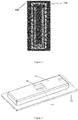
- Fig. 1 shows the structure of an inner side of the first circuit board 100.
- the first circuit board 100 is internally hollowed out.
- the sub-board 103 located in a hollow area inside the first circuit board 100 is connected to one end in the first circuit board 100, on a same plane as the first circuit board 100. Further, the sub-board 103 is attached with a piezoelectric film 101 which is electrically connected thereto, and is also provided with a first connector 102 on the same side as the piezoelectric film 191.
- the sub-board 103 When a pressure stress is applied, the sub-board 103 can be subject to bending deformation in the direction of the pressure stress and by taking one end connected to the first circuit board 100 as a fulcrum. When the pressure stress is released, the sub-board 103 can undergo a reciprocating displacement due to its elasticity.
- the material of the piezoelectric film 101 may be a currently common piezoelectric material, such as polyvinylidene fluoride (PVDF) and polydimethylsiloxane (PDMS), which is not limited herein.
- PVDF polyvinylidene fluoride
- PDMS polydimethylsiloxane
- the sub-board 103 is subject to deformation when a pressure stress is applied thereto, the piezoelectric film 101 will be forced to deform together, so as to generate an electrical signal.
- the electrical signal generated by the piezoelectric film 101 is transferred, via a circuit on the first circuit board 100, to the first connector 102 arranged on the same side as the piezoelectric film 101.
- a tail end of the sub-board 103 is not connected to the circuit board.
- Fig. 2 shows a structural schematic diagram of the second circuit board 200, which is provided with a second connector 201 and an elastic pad 202.
- the second circuit board 200 is also integrated with a signal processing unit (not shown in the figures).
- the second connector 201 and the first connector 102 are arranged opposite to each other and detachably connected to each other.
- the second connector 201 receives the electrical signal transmitted from the first connector 102 and transfers the electrical signal to the signal processing unit, and the signal processing unit responds to the electrical signal and processes it to obtain a test result.
- the second connector 201 supports the first circuit board 100, such that the second connector, as a support, enables the sub-board 103 to deform when subjected to a pressure stress, and enough detectable electrical signals will be generated from the piezoelectric film 101.
- more than two first connectors 102 can be provided, and can be disposed surrounding a hollow area outside the sub-board 103.
- the first connectors 102 and the second connectors 201 are plug-in board-to-board connectors, each of which has a certain height.
- a gap is formed therebetween, and a distance between boards is nominally 0.98 mm.
- the elastic pad 202 is arranged within the foregoing gap and should be in contact with the sub-board 103 and the piezoelectric film 101 for relieving a vibration interference caused by externally induced motion of the entire sensor itself.
- the elastic pad can also support the sub-board 103 and the piezoelectric film 101, and will contribute to generation of a pre-pressure.
- the elastic pad 202 is made of soft silicon gel with a thickness of 1 mm. The thickness of the soft silicon gel is variable with the height of the board-to-board connectors.
- the soft silicon gel optionally has a Shore hardness of 20 to 40, which is adjustable depending on the pressure stress to be measured.
- the elastic pad 202 can also be pressed against the piezoelectric film 101, so as to prevent the latter from accidentally falling off.
- a surface on one side of the second circuit board 200 that is close to the first circuit board 100 is clad with copper, which is used for being grounded, in order to achieve its function of blocking an ambient electromagnetic noise.
- Figs. 3 and 4 show the structure of an outer side of the first circuit board 100.
- the metal shielding 105 generally made of a zinc-copper-nickel alloy, surrounds the sub-board 103 to suppress an ambient electromagnetic noise and to avoid a power frequency electromagnetic interference.
- the metal shielding 105 is provided with a through hole 106.
- a protrusion of an external device under test can penetrate the through hole to apply a pressure stress on the first circuit board.
- the position of the through hole can be selected anywhere on the sub-board 103, merely by allowing the sub-board 103 to deform correspondingly when subjected to the pressure stress.
- the position is also adjustable depending on a range of pressure stress to be measured. For example, when the pressure stress to be measured is relatively small, the through hole can be disposed at the tail end of the sub-board 103, such that the sensor is more sensitive. In contrast, when the pressure stress to be measured is relatively large, the through hole can be alternatively disposed in the middle of the sub-board 103 or a connection end of the sub-board 103.
- the piezoelectric film 101 sandwiched between two shielding layers is shielded by the metal shielding 105 on a top side and is shielded by clad copper of the second circuit board 200 on a bottom side, which jointly suppress an ambient interference.
- both the first circuit board 100 and the second circuit board 200 may be made of a conventional circuit board material FR-4 (a glass fiber epoxy laminate), or may be made of other circuit board materials on which a circuit layout can be designed, for example a composite substrate, such as a single-sided partial-fiberglass plate 22F, a single-sided fiberglass plate CEM-1 and a dual-sided partial-fiberglass plate CEM-3, or a metal substrate.
- FR-4 a glass fiber epoxy laminate
- the board-to-board connectors and the metal shielding 105 are respectively welded to the first circuit board 100 and the second circuit board 200, the piezoelectric film 101 is then attached at room temperature, and the first circuit board 100 and the second circuit board 200 are respectively tested. After the test is completed, the first circuit board 100 is directly plugged onto the second circuit board 200, so as to form the complete piezoelectric sensor.
- the first circuit board 100 is directly detached, so that fault detection can be separately performed, and the piezoelectric film 101 can be conveniently replaced. Moreover, an operation at a high temperature is avoided in the presence of the piezoelectric film, thereby preventing any damage to the piezoelectric film caused by overheating.
- the sensor can be used as an acceleration sensor.
- the sensor vibrates, since there is no elastic pad 202, the sub-board 103 vibrates along with it to force the piezoelectric film 101 to deform, and then a current acceleration value can be accurately obtained by providing the signal processing unit.
Abstract
Description
- The present disclosure relates to the field of piezoelectric sensing, and in particular to a split-type piezoelectric sensor.
- A piezoelectric film, which is a novel high polymer type flexible transduction material, can be machined into a vibration sensor or an accelerometer, which is efficient, reliable and cost-effective, and can also be combined with a suitable circuit to form a wireless detecting and monitoring system. A piezoelectric film sensor is widely used in many fields such as buildings, speed and acceleration measurement, medical physiological signal collection and vehicle theft deterrent owing to numerous advantages of the piezoelectric film sensor.
- Currently, the piezoelectric film sensor is often of a cantilevered beam type, and a piezoelectric film is attached on an inner side of a cantilevered beam. In this way, when an external longitudinal stress is applied to the sensor, a relatively large stress will be transversely generated, so as to generate deformation and thus an electrical signal, which is converted by a signal processing unit to obtain a specific measurement parameter.
- A cantilevered beam structure of an existing piezoelectric film sensor is generally of two types. One is an integrated type, where slotting and hollowing are directly performed on a circuit board capable of signal processing, so as to form the cantilevered beam structure, and a piezoelectric film is then attached on one side of a cantilevered beam that has an electrode (generally on the inner side). However, the attached piezoelectric film is prone to heating influence of the circuit board since the piezoelectric film and a signal processing unit are located on the same circuit board. The bonded piezoelectric film cannot be tested independently. Moreover, an overhaul will be difficult, and after the piezoelectric film is damaged, the sensor must be replaced as a whole, which contributes to increased cost.
- The other one is a welding type or a riveting type, where a metal plate or a ceramic plate is selected to be a cantilevered beam, and the metal plate or the ceramic plate attached with a piezoelectric film by way of welding or riveting is then mounted on a substrate carrying a signal processing unit. A welding or riveting end has functions of both connection and signal transmission. However, the piezoelectric film has low temperature resistance as being a high polymer material. During a welding process, the piezoelectric film is possibly damaged or suffers performance degradation. It could also become difficult to test the bonding quality of the film. In addition, the welding or riveting manner is not conducive to the dismantlement of the sensor. In particular, in the riveting manner, it is only possible to realize dismantlement in a destructive manner, which is not conducive to overhaul and reuse of a piezoelectric film board.
- In view of the above-mentioned disadvantages of existing techniques, an objective of the disclosure is to propose a split-type piezoelectric sensor, in which a piezoelectric film can be flexibly replaced and the performance of the piezoelectric film can be readily tested.
- In order to achieve the above-mentioned objective, the disclosure provides a split-type piezoelectric sensor, including a first circuit board and a second circuit board.
- The first circuit board includes a sub-board, a piezoelectric film, and a first connector. The sub-board and the first circuit board are located on a same plane, and the sub-board is located in a hollow area of the first circuit board and connected to one end in the first circuit board, so that the sub-board is displaceable by taking the end in the first circuit board as a fulcrum. The piezoelectric film is attached to and electrically connected to the sub-board. The first connector and the piezoelectric film are provided on a same side, and the first connector is electrically connected to the first circuit board.
- The second circuit board includes a signal processing unit and a second connector electrically connected to the signal processing unit. The second connector is opposite to and detachably connected to the first connector, and the second connector supports the first circuit board.
- Furthermore, one side of the second circuit board on which the second connector is arranged is clad with copper.
- Furthermore, a plurality of first connectors and a plurality of second connectors are provided, and the first connectors surround the hollow area.
- Furthermore, an elastic pad is provided, which is arranged between the piezoelectric film and the second circuit board.
- Furthermore, a shielding is arranged on a surface of the first circuit board that is opposite to the piezoelectric film, and the shielding surrounds the hollow area.
- Furthermore, the shielding includes a through hole.
- The disclosure has a beneficial effect in that the piezoelectric film and an operation processing unit are separated, the piezoelectric film can be detached and tested at any time, and reuse of a piezoelectric film circuit board can be achieved.
- The concept, specific structure and resulting effect of the disclosure are further described below in conjunction with the accompanying drawings to fully understand the objectives, features, and effects of the disclosure.
- By reading the following detailed description made with reference to the accompanying drawings for non-limiting embodiments, further features, objectives and advantages of the disclosure will become more apparent.
-
Fig.1 is a structural bottom view of a first circuit board of the disclosure; -
Fig. 2 is a structural schematic diagram of a second circuit board of the disclosure; and -
Fig. 3 is a structural top view of the first circuit board of the disclosure; and -
Fig. 4 is a structural perspective view of the first circuit board of the disclosure. - 100-First circuit board; 101-Piezoelectric film; 102-First connector; 103-Sub-board; 104-Metal shielding welding spot; 105-Metal shielding; 106-Through hole; 200-Second circuit board; 201-Second connector; and 202-Elastic pad.
- Preferred embodiments of the disclosure are described below with reference to the accompanying drawings of the description to make the disclosed contents clearer and easier to understand. The disclosure can be embodied in various implementations of embodiments, and the scope of the disclosure is not limited to the embodiments mentioned herein.
- In the accompanying drawings, an identical reference number indicates components having identical structure, and similar reference numbers indicate assemblies having similar structures or functions throughout. The size and thickness of each assembly shown in the figures are shown arbitrarily, and the disclosure does not define the size and thickness of each assembly. In order to make the illustration clearer, the thickness of the component in some individual places of the accompanying drawings is appropriately exaggerated.
-
Fig. 1 shows the structure of an inner side of thefirst circuit board 100. Thefirst circuit board 100 is internally hollowed out. Thesub-board 103 located in a hollow area inside thefirst circuit board 100 is connected to one end in thefirst circuit board 100, on a same plane as thefirst circuit board 100. Further, thesub-board 103 is attached with apiezoelectric film 101 which is electrically connected thereto, and is also provided with afirst connector 102 on the same side as the piezoelectric film 191. - When a pressure stress is applied, the
sub-board 103 can be subject to bending deformation in the direction of the pressure stress and by taking one end connected to thefirst circuit board 100 as a fulcrum. When the pressure stress is released, thesub-board 103 can undergo a reciprocating displacement due to its elasticity. - The material of the
piezoelectric film 101 may be a currently common piezoelectric material, such as polyvinylidene fluoride (PVDF) and polydimethylsiloxane (PDMS), which is not limited herein. Thesub-board 103 is subject to deformation when a pressure stress is applied thereto, thepiezoelectric film 101 will be forced to deform together, so as to generate an electrical signal. The electrical signal generated by thepiezoelectric film 101 is transferred, via a circuit on thefirst circuit board 100, to thefirst connector 102 arranged on the same side as thepiezoelectric film 101. - Certainly, in order to generate the reciprocating displacement, a tail end of the
sub-board 103 is not connected to the circuit board. In addition, it is necessary to reserve a part of space between thefirst circuit board 100 and thesecond circuit board 200 in order to provide a sufficient freedom for the displacement of thesub-board 103. -
Fig. 2 shows a structural schematic diagram of thesecond circuit board 200, which is provided with asecond connector 201 and anelastic pad 202. In addition, thesecond circuit board 200 is also integrated with a signal processing unit (not shown in the figures). - The
second connector 201 and thefirst connector 102 are arranged opposite to each other and detachably connected to each other. Thesecond connector 201 receives the electrical signal transmitted from thefirst connector 102 and transfers the electrical signal to the signal processing unit, and the signal processing unit responds to the electrical signal and processes it to obtain a test result. During operation of a sensor, thesecond connector 201 supports thefirst circuit board 100, such that the second connector, as a support, enables thesub-board 103 to deform when subjected to a pressure stress, and enough detectable electrical signals will be generated from thepiezoelectric film 101. - In order to realize a more stable support for the
first circuit board 100, more than twofirst connectors 102, as well as more than two second connectors opposite thereto, can be provided, and can be disposed surrounding a hollow area outside the sub-board 103. - In the embodiment, the
first connectors 102 and thesecond connectors 201 are plug-in board-to-board connectors, each of which has a certain height. When thefirst circuit board 100 and thesecond circuit board 200 are arranged in connection, a gap is formed therebetween, and a distance between boards is nominally 0.98 mm. - The
elastic pad 202 is arranged within the foregoing gap and should be in contact with the sub-board 103 and thepiezoelectric film 101 for relieving a vibration interference caused by externally induced motion of the entire sensor itself. The elastic pad can also support the sub-board 103 and thepiezoelectric film 101, and will contribute to generation of a pre-pressure. In this embodiment, theelastic pad 202 is made of soft silicon gel with a thickness of 1 mm. The thickness of the soft silicon gel is variable with the height of the board-to-board connectors. The soft silicon gel optionally has a Shore hardness of 20 to 40, which is adjustable depending on the pressure stress to be measured. In addition, theelastic pad 202 can also be pressed against thepiezoelectric film 101, so as to prevent the latter from accidentally falling off. - Furthermore, a surface on one side of the
second circuit board 200 that is close to thefirst circuit board 100 is clad with copper, which is used for being grounded, in order to achieve its function of blocking an ambient electromagnetic noise. -
Figs. 3 and 4 show the structure of an outer side of thefirst circuit board 100. There is a metal shielding 105 outside the hollow area. The metal shielding 105, generally made of a zinc-copper-nickel alloy, surrounds the sub-board 103 to suppress an ambient electromagnetic noise and to avoid a power frequency electromagnetic interference. - The metal shielding 105 is provided with a through
hole 106. During use of the sensor, a protrusion of an external device under test can penetrate the through hole to apply a pressure stress on the first circuit board. The position of the through hole can be selected anywhere on the sub-board 103, merely by allowing the sub-board 103 to deform correspondingly when subjected to the pressure stress. The position is also adjustable depending on a range of pressure stress to be measured. For example, when the pressure stress to be measured is relatively small, the through hole can be disposed at the tail end of the sub-board 103, such that the sensor is more sensitive. In contrast, when the pressure stress to be measured is relatively large, the through hole can be alternatively disposed in the middle of the sub-board 103 or a connection end of the sub-board 103. - In one embodiment, during operation of the sensor, the
piezoelectric film 101 sandwiched between two shielding layers is shielded by the metal shielding 105 on a top side and is shielded by clad copper of thesecond circuit board 200 on a bottom side, which jointly suppress an ambient interference. - Furthermore, both the
first circuit board 100 and thesecond circuit board 200 may be made of a conventional circuit board material FR-4 (a glass fiber epoxy laminate), or may be made of other circuit board materials on which a circuit layout can be designed, for example a composite substrate, such as a single-sided partial-fiberglass plate 22F, a single-sided fiberglass plate CEM-1 and a dual-sided partial-fiberglass plate CEM-3, or a metal substrate. - During manufacturing of the sensor, firstly, the board-to-board connectors and the metal shielding 105 are respectively welded to the
first circuit board 100 and thesecond circuit board 200, thepiezoelectric film 101 is then attached at room temperature, and thefirst circuit board 100 and thesecond circuit board 200 are respectively tested. After the test is completed, thefirst circuit board 100 is directly plugged onto thesecond circuit board 200, so as to form the complete piezoelectric sensor. During overhaul of the sensor, thefirst circuit board 100 is directly detached, so that fault detection can be separately performed, and thepiezoelectric film 101 can be conveniently replaced. Moreover, an operation at a high temperature is avoided in the presence of the piezoelectric film, thereby preventing any damage to the piezoelectric film caused by overheating. - Furthermore, it is also possible to provide no
elastic pad 202 in the gap between thefirst circuit board 100 and thesecond circuit board 200, in which case the sensor can be used as an acceleration sensor. When the sensor vibrates, since there is noelastic pad 202, the sub-board 103 vibrates along with it to force thepiezoelectric film 101 to deform, and then a current acceleration value can be accurately obtained by providing the signal processing unit. - The preferred embodiments of the disclosure have been described in detail above. It should be understood that those of ordinary skill in the art would be able to make various modifications and variations according to the concept of the disclosure without involving any inventive effort. Therefore, any solution that can be obtained by those skilled in the art by logical analysis, reasoning or limited trials on the basis of the prior art and according to the concept of the disclosure should be included within the scope of the claims.
Claims (6)
- A split-type piezoelectric sensor, characterized by comprising a first circuit board and a second circuit board,wherein the first circuit board comprises a sub-board, a piezoelectric film, and a first connector, wherein the sub-board and the first circuit board are located on a same plane, and the sub-board is located in a hollow area of the first circuit board and connected to one end in the first circuit board, so that the sub-board is displaceable by taking the end in the first circuit board as a fulcrum, wherein the piezoelectric film is attached to electrically connected to the sub-board, and wherein the first connector and the piezoelectric film are provided on a same side, and the first connector is electrically connected to the first circuit board; andwherein the second circuit board includes a signal processing unit and a second connector electrically connected to the signal processing unit, and wherein the second connector is opposite to and detachably connected to the first connector, and the second connector supports the first circuit board.
- The split-type piezoelectric sensor according to claim 1, characterized in that one side of the second circuit board on which the second connector is arranged is clad with copper.
- The split-type piezoelectric sensor according to claim 1, characterized in that a plurality of first connectors and a plurality of second connectors are provided, and the first connectors surround the hollow area.
- The split-type piezoelectric sensor according to claim 1, characterized by further comprising an elastic pad, which is arranged between the piezoelectric film and the second circuit board.
- The split-type piezoelectric sensor according to any one of claims 1 to 4, characterized in that a shielding is arranged on a surface of the first circuit board that is opposite to the piezoelectric film, and the shielding surrounds the hollow area.
- The split-type piezoelectric sensor according to claim 5, characterized in that the shielding comprises a through hole.
Applications Claiming Priority (3)
| Application Number | Priority Date | Filing Date | Title |
|---|---|---|---|
| CN201922450236 | 2019-12-26 | ||
| CN202010253531.7A CN111649767A (en) | 2019-12-26 | 2020-04-01 | Split type piezoelectric sensor |
| PCT/CN2021/078462 WO2021196944A1 (en) | 2019-12-26 | 2021-03-01 | Split-type piezoelectric sensor |
Publications (2)
| Publication Number | Publication Date |
|---|---|
| EP4130680A1 true EP4130680A1 (en) | 2023-02-08 |
| EP4130680A4 EP4130680A4 (en) | 2024-04-10 |
Family
ID=72352076
Family Applications (1)
| Application Number | Title | Priority Date | Filing Date |
|---|---|---|---|
| EP21780471.5A Pending EP4130680A4 (en) | 2019-12-26 | 2021-03-01 | Split-type piezoelectric sensor |
Country Status (3)
| Country | Link |
|---|---|
| EP (1) | EP4130680A4 (en) |
| CN (2) | CN212567429U (en) |
| WO (1) | WO2021196944A1 (en) |
Families Citing this family (3)
| Publication number | Priority date | Publication date | Assignee | Title |
|---|---|---|---|---|
| CN212567429U (en) * | 2019-12-26 | 2021-02-19 | 麒盛科技股份有限公司 | Split type piezoelectric sensor |
| CN114305395A (en) * | 2020-09-29 | 2022-04-12 | 麒盛科技股份有限公司 | Physiological signal detection sensor with environmental vibration compensation |
| CN114486043A (en) * | 2022-01-26 | 2022-05-13 | 浙江清华长三角研究院 | Sensor capable of measuring tension of binding band in real time |
Family Cites Families (6)
| Publication number | Priority date | Publication date | Assignee | Title |
|---|---|---|---|---|
| JP2013178241A (en) * | 2012-02-07 | 2013-09-09 | Sumitomo Electric Ind Ltd | Pressure-sensitive sensor mounting wiring board |
| CN108061563A (en) * | 2017-11-21 | 2018-05-22 | 麒盛科技股份有限公司 | Cantilever piezoelectric film small-signal sensor |
| CN108398181A (en) * | 2018-02-06 | 2018-08-14 | 麒盛科技股份有限公司 | Integral type bio-signal acquisition sensor |
| CN208350246U (en) * | 2018-06-11 | 2019-01-08 | 上海智杰自动化设备有限公司 | A kind of force snesor of direct measurement terminal crimp force |
| CN209609993U (en) * | 2018-11-26 | 2019-11-12 | 河南师范大学 | A kind of foot force Timing acquisition device based on piezoelectric sensor |
| CN212567429U (en) * | 2019-12-26 | 2021-02-19 | 麒盛科技股份有限公司 | Split type piezoelectric sensor |
-
2020
- 2020-04-01 CN CN202020461831.XU patent/CN212567429U/en active Active
- 2020-04-01 CN CN202010253531.7A patent/CN111649767A/en active Pending
-
2021
- 2021-03-01 EP EP21780471.5A patent/EP4130680A4/en active Pending
- 2021-03-01 WO PCT/CN2021/078462 patent/WO2021196944A1/en active Application Filing
Also Published As
| Publication number | Publication date |
|---|---|
| CN111649767A (en) | 2020-09-11 |
| CN212567429U (en) | 2021-02-19 |
| EP4130680A4 (en) | 2024-04-10 |
| WO2021196944A1 (en) | 2021-10-07 |
Similar Documents
| Publication | Publication Date | Title |
|---|---|---|
| EP4130680A1 (en) | Split-type piezoelectric sensor | |
| JP5384678B2 (en) | Ultrasonic probe and ultrasonic diagnostic apparatus using the same | |
| US20060154398A1 (en) | Method of manufacturing a structural health monitoring layer | |
| JP6301948B2 (en) | Measuring device and component with built-in measuring device | |
| KR20060050752A (en) | Acceleration sensor | |
| JP6776152B2 (en) | A strain-causing body and a force sensor equipped with the strain-causing body | |
| KR101127711B1 (en) | A microphone component and a method for its manufacture | |
| JP2782940B2 (en) | Floating magnetic head device | |
| JP2018048915A (en) | Force sensor | |
| WO2021191948A1 (en) | Substrate module for measuring vibration and vibration detection device | |
| WO2018154898A1 (en) | Elastic body and force sensor provided with said elastic body | |
| CN211090109U (en) | PCB and MEMS sensor applying same | |
| JPH08261857A (en) | Pressure sensor | |
| US20220155169A1 (en) | Capacitive Pressure Sensor, Manufacturing Method Thereof, and Capacitive Pressure Sensor Device | |
| JP6324803B2 (en) | Pressure-sensitive sensor and manufacturing method thereof | |
| CN113432773B (en) | Sensor suitable for measuring pressure of shock wave on surface of flexible object and manufacturing method | |
| CN210641123U (en) | PCB and MEMS sensor applying same | |
| JPS6238323A (en) | Vibration detection probe | |
| EP2717059B1 (en) | Acceleration sensor | |
| JP2018138890A (en) | Strain body and force sensor having the strain body | |
| JP2014085259A (en) | Strain gauge, strain measuring device and strain gauge type converter | |
| KR101572118B1 (en) | Flip-chip bonding device used in contact condition | |
| JP2006038824A (en) | Semiconductor sensor device | |
| US20220039748A1 (en) | Piezoelectric sensor | |
| US20220344572A1 (en) | Deformation detection sensor |
Legal Events
| Date | Code | Title | Description |
|---|---|---|---|
| STAA | Information on the status of an ep patent application or granted ep patent |
Free format text: STATUS: THE INTERNATIONAL PUBLICATION HAS BEEN MADE |
|
| PUAI | Public reference made under article 153(3) epc to a published international application that has entered the european phase |
Free format text: ORIGINAL CODE: 0009012 |
|
| STAA | Information on the status of an ep patent application or granted ep patent |
Free format text: STATUS: REQUEST FOR EXAMINATION WAS MADE |
|
| 17P | Request for examination filed |
Effective date: 20220715 |
|
| AK | Designated contracting states |
Kind code of ref document: A1 Designated state(s): AL AT BE BG CH CY CZ DE DK EE ES FI FR GB GR HR HU IE IS IT LI LT LU LV MC MK MT NL NO PL PT RO RS SE SI SK SM TR |
|
| DAV | Request for validation of the european patent (deleted) | ||
| DAX | Request for extension of the european patent (deleted) | ||
| A4 | Supplementary search report drawn up and despatched |
Effective date: 20240314 |
|
| RIC1 | Information provided on ipc code assigned before grant |
Ipc: G01P 15/09 20060101ALI20240307BHEP Ipc: G01L 19/14 20060101ALI20240307BHEP Ipc: G01L 19/06 20060101ALI20240307BHEP Ipc: G01L 9/00 20060101ALI20240307BHEP Ipc: G01D 11/00 20060101ALI20240307BHEP Ipc: G01L 1/18 20060101ALI20240307BHEP Ipc: G01L 1/16 20060101ALI20240307BHEP Ipc: G01D 5/12 20060101AFI20240307BHEP |