EP4130346A1 - Laminate, metal plating liquid, and laminate manufacturing method - Google Patents
Laminate, metal plating liquid, and laminate manufacturing method Download PDFInfo
- Publication number
- EP4130346A1 EP4130346A1 EP20929210.1A EP20929210A EP4130346A1 EP 4130346 A1 EP4130346 A1 EP 4130346A1 EP 20929210 A EP20929210 A EP 20929210A EP 4130346 A1 EP4130346 A1 EP 4130346A1
- Authority
- EP
- European Patent Office
- Prior art keywords
- metal
- metal element
- laminate
- films
- interface layer
- Prior art date
- Legal status (The legal status is an assumption and is not a legal conclusion. Google has not performed a legal analysis and makes no representation as to the accuracy of the status listed.)
- Pending
Links
- 229910052751 metal Inorganic materials 0.000 title claims abstract description 242
- 239000002184 metal Substances 0.000 title claims abstract description 235
- 238000004519 manufacturing process Methods 0.000 title claims abstract description 21
- 238000007747 plating Methods 0.000 title claims description 90
- 239000007788 liquid Substances 0.000 title 1
- 239000000758 substrate Substances 0.000 claims abstract description 22
- 229910052759 nickel Inorganic materials 0.000 claims abstract description 13
- 229910052721 tungsten Inorganic materials 0.000 claims abstract description 11
- 229910052804 chromium Inorganic materials 0.000 claims abstract description 9
- 239000010949 copper Substances 0.000 claims description 44
- 150000003839 salts Chemical class 0.000 claims description 19
- 229910052802 copper Inorganic materials 0.000 claims description 16
- 150000001875 compounds Chemical class 0.000 claims description 15
- 239000000654 additive Substances 0.000 claims description 13
- 229910052718 tin Inorganic materials 0.000 claims description 13
- 229910052725 zinc Inorganic materials 0.000 claims description 11
- 229910052738 indium Inorganic materials 0.000 claims description 10
- 229910052717 sulfur Inorganic materials 0.000 claims description 10
- 230000000996 additive effect Effects 0.000 claims description 8
- 229910052787 antimony Inorganic materials 0.000 claims description 7
- JZCCFEFSEZPSOG-UHFFFAOYSA-L copper(II) sulfate pentahydrate Chemical compound O.O.O.O.O.[Cu+2].[O-]S([O-])(=O)=O JZCCFEFSEZPSOG-UHFFFAOYSA-L 0.000 claims description 7
- 229910052797 bismuth Inorganic materials 0.000 claims description 6
- 229910052698 phosphorus Inorganic materials 0.000 claims description 6
- NINIDFKCEFEMDL-UHFFFAOYSA-N Sulfur Chemical compound [S] NINIDFKCEFEMDL-UHFFFAOYSA-N 0.000 claims description 5
- CVHZOJJKTDOEJC-UHFFFAOYSA-N saccharin Chemical compound C1=CC=C2C(=O)NS(=O)(=O)C2=C1 CVHZOJJKTDOEJC-UHFFFAOYSA-N 0.000 claims description 5
- 239000011593 sulfur Substances 0.000 claims description 5
- ABLZXFCXXLZCGV-UHFFFAOYSA-N Phosphorous acid Chemical compound OP(O)=O ABLZXFCXXLZCGV-UHFFFAOYSA-N 0.000 claims description 4
- 229940081974 saccharin Drugs 0.000 claims description 4
- 235000019204 saccharin Nutrition 0.000 claims description 4
- 239000000901 saccharin and its Na,K and Ca salt Substances 0.000 claims description 4
- 239000013078 crystal Substances 0.000 claims description 3
- RYGMFSIKBFXOCR-UHFFFAOYSA-N Copper Chemical group [Cu] RYGMFSIKBFXOCR-UHFFFAOYSA-N 0.000 claims description 2
- 229910052796 boron Inorganic materials 0.000 claims description 2
- 238000006243 chemical reaction Methods 0.000 claims description 2
- 239000008139 complexing agent Substances 0.000 claims description 2
- 239000003002 pH adjusting agent Substances 0.000 claims description 2
- 239000011574 phosphorus Substances 0.000 claims description 2
- OAICVXFJPJFONN-UHFFFAOYSA-N Phosphorus Chemical compound [P] OAICVXFJPJFONN-UHFFFAOYSA-N 0.000 claims 1
- 239000011651 chromium Substances 0.000 abstract description 10
- 230000007797 corrosion Effects 0.000 abstract description 9
- 238000005260 corrosion Methods 0.000 abstract description 9
- JOPOVCBBYLSVDA-UHFFFAOYSA-N chromium(6+) Chemical compound [Cr+6] JOPOVCBBYLSVDA-UHFFFAOYSA-N 0.000 abstract description 8
- 239000010408 film Substances 0.000 description 183
- 239000010410 layer Substances 0.000 description 129
- PXHVJJICTQNCMI-UHFFFAOYSA-N nickel Substances [Ni] PXHVJJICTQNCMI-UHFFFAOYSA-N 0.000 description 46
- 230000000052 comparative effect Effects 0.000 description 21
- 238000000034 method Methods 0.000 description 20
- 238000012360 testing method Methods 0.000 description 14
- 238000009713 electroplating Methods 0.000 description 13
- 230000008569 process Effects 0.000 description 11
- 239000011135 tin Substances 0.000 description 11
- 238000000137 annealing Methods 0.000 description 10
- 229910000990 Ni alloy Inorganic materials 0.000 description 9
- 230000000694 effects Effects 0.000 description 9
- 239000002356 single layer Substances 0.000 description 9
- 239000011701 zinc Substances 0.000 description 9
- 238000000329 molecular dynamics simulation Methods 0.000 description 8
- 238000010008 shearing Methods 0.000 description 8
- 238000011156 evaluation Methods 0.000 description 7
- 239000000126 substance Substances 0.000 description 7
- 239000002245 particle Substances 0.000 description 6
- 229910052692 Dysprosium Inorganic materials 0.000 description 5
- 229910052691 Erbium Inorganic materials 0.000 description 5
- 229910052693 Europium Inorganic materials 0.000 description 5
- 229910052689 Holmium Inorganic materials 0.000 description 5
- 229910052779 Neodymium Inorganic materials 0.000 description 5
- 229910052772 Samarium Inorganic materials 0.000 description 5
- 229910052771 Terbium Inorganic materials 0.000 description 5
- 229910052775 Thulium Inorganic materials 0.000 description 5
- 229910052769 Ytterbium Inorganic materials 0.000 description 5
- 229910052783 alkali metal Inorganic materials 0.000 description 5
- 150000001340 alkali metals Chemical class 0.000 description 5
- 229910052784 alkaline earth metal Inorganic materials 0.000 description 5
- 150000001342 alkaline earth metals Chemical class 0.000 description 5
- 230000015572 biosynthetic process Effects 0.000 description 5
- 238000005868 electrolysis reaction Methods 0.000 description 5
- 229910052733 gallium Inorganic materials 0.000 description 5
- 229910052742 iron Inorganic materials 0.000 description 5
- 229910052745 lead Inorganic materials 0.000 description 5
- 229910052748 manganese Inorganic materials 0.000 description 5
- 239000011572 manganese Substances 0.000 description 5
- 238000001878 scanning electron micrograph Methods 0.000 description 5
- 229910052716 thallium Inorganic materials 0.000 description 5
- GWEVSGVZZGPLCZ-UHFFFAOYSA-N Titan oxide Chemical compound O=[Ti]=O GWEVSGVZZGPLCZ-UHFFFAOYSA-N 0.000 description 4
- 239000003795 chemical substances by application Substances 0.000 description 4
- 229910052732 germanium Inorganic materials 0.000 description 4
- 229910052752 metalloid Inorganic materials 0.000 description 4
- -1 ZnF Chemical compound 0.000 description 3
- 229910052793 cadmium Inorganic materials 0.000 description 3
- 230000032798 delamination Effects 0.000 description 3
- 238000009826 distribution Methods 0.000 description 3
- 229910052737 gold Inorganic materials 0.000 description 3
- 230000006872 improvement Effects 0.000 description 3
- 239000000463 material Substances 0.000 description 3
- 238000005259 measurement Methods 0.000 description 3
- 150000002739 metals Chemical class 0.000 description 3
- 239000000203 mixture Substances 0.000 description 3
- 229910052709 silver Inorganic materials 0.000 description 3
- 230000001629 suppression Effects 0.000 description 3
- 238000004381 surface treatment Methods 0.000 description 3
- OKTJSMMVPCPJKN-UHFFFAOYSA-N Carbon Chemical compound [C] OKTJSMMVPCPJKN-UHFFFAOYSA-N 0.000 description 2
- VEXZGXHMUGYJMC-UHFFFAOYSA-M Chloride anion Chemical compound [Cl-] VEXZGXHMUGYJMC-UHFFFAOYSA-M 0.000 description 2
- ATJFFYVFTNAWJD-UHFFFAOYSA-N Tin Chemical compound [Sn] ATJFFYVFTNAWJD-UHFFFAOYSA-N 0.000 description 2
- 238000002441 X-ray diffraction Methods 0.000 description 2
- 229910045601 alloy Inorganic materials 0.000 description 2
- 239000000956 alloy Substances 0.000 description 2
- PNEYBMLMFCGWSK-UHFFFAOYSA-N aluminium oxide Inorganic materials [O-2].[O-2].[O-2].[Al+3].[Al+3] PNEYBMLMFCGWSK-UHFFFAOYSA-N 0.000 description 2
- 238000004458 analytical method Methods 0.000 description 2
- 230000008901 benefit Effects 0.000 description 2
- 229910052790 beryllium Inorganic materials 0.000 description 2
- 230000033228 biological regulation Effects 0.000 description 2
- 230000015556 catabolic process Effects 0.000 description 2
- 150000001805 chlorine compounds Chemical class 0.000 description 2
- 239000002131 composite material Substances 0.000 description 2
- 229910052593 corundum Inorganic materials 0.000 description 2
- 230000006378 damage Effects 0.000 description 2
- 238000006731 degradation reaction Methods 0.000 description 2
- 238000005238 degreasing Methods 0.000 description 2
- 238000013461 design Methods 0.000 description 2
- 229910003460 diamond Inorganic materials 0.000 description 2
- 239000010432 diamond Substances 0.000 description 2
- 239000010931 gold Substances 0.000 description 2
- 229910002804 graphite Inorganic materials 0.000 description 2
- 239000010439 graphite Substances 0.000 description 2
- 239000012535 impurity Substances 0.000 description 2
- 229910052961 molybdenite Inorganic materials 0.000 description 2
- CWQXQMHSOZUFJS-UHFFFAOYSA-N molybdenum disulfide Chemical compound S=[Mo]=S CWQXQMHSOZUFJS-UHFFFAOYSA-N 0.000 description 2
- 229910052982 molybdenum disulfide Inorganic materials 0.000 description 2
- LAIZPRYFQUWUBN-UHFFFAOYSA-L nickel chloride hexahydrate Chemical compound O.O.O.O.O.O.[Cl-].[Cl-].[Ni+2] LAIZPRYFQUWUBN-UHFFFAOYSA-L 0.000 description 2
- RRIWRJBSCGCBID-UHFFFAOYSA-L nickel sulfate hexahydrate Chemical compound O.O.O.O.O.O.[Ni+2].[O-]S([O-])(=O)=O RRIWRJBSCGCBID-UHFFFAOYSA-L 0.000 description 2
- 229940116202 nickel sulfate hexahydrate Drugs 0.000 description 2
- 150000002894 organic compounds Chemical class 0.000 description 2
- 238000005554 pickling Methods 0.000 description 2
- 239000002243 precursor Substances 0.000 description 2
- 238000002203 pretreatment Methods 0.000 description 2
- 239000002994 raw material Substances 0.000 description 2
- 230000009467 reduction Effects 0.000 description 2
- 239000011347 resin Substances 0.000 description 2
- 229920005989 resin Polymers 0.000 description 2
- 239000000523 sample Substances 0.000 description 2
- 239000010944 silver (metal) Substances 0.000 description 2
- 238000004088 simulation Methods 0.000 description 2
- NLJMYIDDQXHKNR-UHFFFAOYSA-K sodium citrate Chemical compound O.O.[Na+].[Na+].[Na+].[O-]C(=O)CC(O)(CC([O-])=O)C([O-])=O NLJMYIDDQXHKNR-UHFFFAOYSA-K 0.000 description 2
- 239000007787 solid Substances 0.000 description 2
- 238000004544 sputter deposition Methods 0.000 description 2
- 229910001220 stainless steel Inorganic materials 0.000 description 2
- 239000010935 stainless steel Substances 0.000 description 2
- 150000004763 sulfides Chemical class 0.000 description 2
- UMGDCJDMYOKAJW-UHFFFAOYSA-N thiourea Chemical compound NC(N)=S UMGDCJDMYOKAJW-UHFFFAOYSA-N 0.000 description 2
- 229910003470 tongbaite Inorganic materials 0.000 description 2
- 229910001845 yogo sapphire Inorganic materials 0.000 description 2
- 229910000851 Alloy steel Inorganic materials 0.000 description 1
- 229910000975 Carbon steel Inorganic materials 0.000 description 1
- 229910020515 Co—W Inorganic materials 0.000 description 1
- 229910017709 Ni Co Inorganic materials 0.000 description 1
- 229910003267 Ni-Co Inorganic materials 0.000 description 1
- 229910018104 Ni-P Inorganic materials 0.000 description 1
- 229910021586 Nickel(II) chloride Inorganic materials 0.000 description 1
- 229910003262 Ni‐Co Inorganic materials 0.000 description 1
- 229910018487 Ni—Cr Inorganic materials 0.000 description 1
- 229910018536 Ni—P Inorganic materials 0.000 description 1
- WINXNKPZLFISPD-UHFFFAOYSA-M Saccharin sodium Chemical compound [Na+].C1=CC=C2C(=O)[N-]S(=O)(=O)C2=C1 WINXNKPZLFISPD-UHFFFAOYSA-M 0.000 description 1
- 229910000831 Steel Inorganic materials 0.000 description 1
- LSNNMFCWUKXFEE-UHFFFAOYSA-N Sulfurous acid Chemical compound OS(O)=O LSNNMFCWUKXFEE-UHFFFAOYSA-N 0.000 description 1
- UCKMPCXJQFINFW-UHFFFAOYSA-N Sulphide Chemical compound [S-2] UCKMPCXJQFINFW-UHFFFAOYSA-N 0.000 description 1
- XSQUKJJJFZCRTK-UHFFFAOYSA-N Urea Natural products NC(N)=O XSQUKJJJFZCRTK-UHFFFAOYSA-N 0.000 description 1
- 239000000853 adhesive Substances 0.000 description 1
- 230000001070 adhesive effect Effects 0.000 description 1
- 239000012790 adhesive layer Substances 0.000 description 1
- 238000004220 aggregation Methods 0.000 description 1
- 230000002776 aggregation Effects 0.000 description 1
- 229910052782 aluminium Inorganic materials 0.000 description 1
- XAGFODPZIPBFFR-UHFFFAOYSA-N aluminium Chemical compound [Al] XAGFODPZIPBFFR-UHFFFAOYSA-N 0.000 description 1
- 238000013475 authorization Methods 0.000 description 1
- 230000006399 behavior Effects 0.000 description 1
- 229910000380 bismuth sulfate Inorganic materials 0.000 description 1
- KGBXLFKZBHKPEV-UHFFFAOYSA-N boric acid Chemical compound OB(O)O KGBXLFKZBHKPEV-UHFFFAOYSA-N 0.000 description 1
- 239000004327 boric acid Substances 0.000 description 1
- 150000001639 boron compounds Chemical class 0.000 description 1
- 238000004364 calculation method Methods 0.000 description 1
- 239000010962 carbon steel Substances 0.000 description 1
- 230000008859 change Effects 0.000 description 1
- 239000003638 chemical reducing agent Substances 0.000 description 1
- GVPFVAHMJGGAJG-UHFFFAOYSA-L cobalt dichloride Chemical compound [Cl-].[Cl-].[Co+2] GVPFVAHMJGGAJG-UHFFFAOYSA-L 0.000 description 1
- 229910000361 cobalt sulfate Inorganic materials 0.000 description 1
- 229940044175 cobalt sulfate Drugs 0.000 description 1
- KTVIXTQDYHMGHF-UHFFFAOYSA-L cobalt(2+) sulfate Chemical compound [Co+2].[O-]S([O-])(=O)=O KTVIXTQDYHMGHF-UHFFFAOYSA-L 0.000 description 1
- 238000010276 construction Methods 0.000 description 1
- 229910000365 copper sulfate Inorganic materials 0.000 description 1
- ORTQZVOHEJQUHG-UHFFFAOYSA-L copper(II) chloride Chemical compound Cl[Cu]Cl ORTQZVOHEJQUHG-UHFFFAOYSA-L 0.000 description 1
- ARUVKPQLZAKDPS-UHFFFAOYSA-L copper(II) sulfate Chemical compound [Cu+2].[O-][S+2]([O-])([O-])[O-] ARUVKPQLZAKDPS-UHFFFAOYSA-L 0.000 description 1
- 230000002596 correlated effect Effects 0.000 description 1
- 230000003247 decreasing effect Effects 0.000 description 1
- 230000006735 deficit Effects 0.000 description 1
- 238000010612 desalination reaction Methods 0.000 description 1
- 238000010586 diagram Methods 0.000 description 1
- BEQZMQXCOWIHRY-UHFFFAOYSA-H dibismuth;trisulfate Chemical compound [Bi+3].[Bi+3].[O-]S([O-])(=O)=O.[O-]S([O-])(=O)=O.[O-]S([O-])(=O)=O BEQZMQXCOWIHRY-UHFFFAOYSA-H 0.000 description 1
- 238000004090 dissolution Methods 0.000 description 1
- 238000001035 drying Methods 0.000 description 1
- 230000007613 environmental effect Effects 0.000 description 1
- 238000002474 experimental method Methods 0.000 description 1
- 230000005283 ground state Effects 0.000 description 1
- 230000001771 impaired effect Effects 0.000 description 1
- 238000010348 incorporation Methods 0.000 description 1
- 229910000337 indium(III) sulfate Inorganic materials 0.000 description 1
- XGCKLPDYTQRDTR-UHFFFAOYSA-H indium(iii) sulfate Chemical compound [In+3].[In+3].[O-]S([O-])(=O)=O.[O-]S([O-])(=O)=O.[O-]S([O-])(=O)=O XGCKLPDYTQRDTR-UHFFFAOYSA-H 0.000 description 1
- 238000003475 lamination Methods 0.000 description 1
- 238000005461 lubrication Methods 0.000 description 1
- 238000012423 maintenance Methods 0.000 description 1
- 229940099596 manganese sulfate Drugs 0.000 description 1
- 239000011702 manganese sulphate Substances 0.000 description 1
- 235000007079 manganese sulphate Nutrition 0.000 description 1
- SQQMAOCOWKFBNP-UHFFFAOYSA-L manganese(II) sulfate Chemical compound [Mn+2].[O-]S([O-])(=O)=O SQQMAOCOWKFBNP-UHFFFAOYSA-L 0.000 description 1
- 230000013011 mating Effects 0.000 description 1
- 238000002844 melting Methods 0.000 description 1
- 230000008018 melting Effects 0.000 description 1
- 230000007935 neutral effect Effects 0.000 description 1
- QMMRZOWCJAIUJA-UHFFFAOYSA-L nickel dichloride Chemical compound Cl[Ni]Cl QMMRZOWCJAIUJA-UHFFFAOYSA-L 0.000 description 1
- LGQLOGILCSXPEA-UHFFFAOYSA-L nickel sulfate Chemical compound [Ni+2].[O-]S([O-])(=O)=O LGQLOGILCSXPEA-UHFFFAOYSA-L 0.000 description 1
- 229940053662 nickel sulfate Drugs 0.000 description 1
- 229910000363 nickel(II) sulfate Inorganic materials 0.000 description 1
- 229910052757 nitrogen Inorganic materials 0.000 description 1
- 238000005498 polishing Methods 0.000 description 1
- 238000010248 power generation Methods 0.000 description 1
- 238000002360 preparation method Methods 0.000 description 1
- UIIIBRHUICCMAI-UHFFFAOYSA-N prop-2-ene-1-sulfonic acid Chemical compound OS(=O)(=O)CC=C UIIIBRHUICCMAI-UHFFFAOYSA-N 0.000 description 1
- 230000000644 propagated effect Effects 0.000 description 1
- 239000013535 sea water Substances 0.000 description 1
- 235000019333 sodium laurylsulphate Nutrition 0.000 description 1
- 238000001179 sorption measurement Methods 0.000 description 1
- 239000010959 steel Substances 0.000 description 1
- YOUIDGQAIILFBW-UHFFFAOYSA-J tetrachlorotungsten Chemical compound Cl[W](Cl)(Cl)Cl YOUIDGQAIILFBW-UHFFFAOYSA-J 0.000 description 1
- 239000010409 thin film Substances 0.000 description 1
- FAKFSJNVVCGEEI-UHFFFAOYSA-J tin(4+);disulfate Chemical compound [Sn+4].[O-]S([O-])(=O)=O.[O-]S([O-])(=O)=O FAKFSJNVVCGEEI-UHFFFAOYSA-J 0.000 description 1
- RZLVQBNCHSJZPX-UHFFFAOYSA-L zinc sulfate heptahydrate Chemical compound O.O.O.O.O.O.O.[Zn+2].[O-]S([O-])(=O)=O RZLVQBNCHSJZPX-UHFFFAOYSA-L 0.000 description 1
Images




Classifications
-
- B—PERFORMING OPERATIONS; TRANSPORTING
- B32—LAYERED PRODUCTS
- B32B—LAYERED PRODUCTS, i.e. PRODUCTS BUILT-UP OF STRATA OF FLAT OR NON-FLAT, e.g. CELLULAR OR HONEYCOMB, FORM
- B32B15/00—Layered products comprising a layer of metal
- B32B15/01—Layered products comprising a layer of metal all layers being exclusively metallic
-
- C—CHEMISTRY; METALLURGY
- C23—COATING METALLIC MATERIAL; COATING MATERIAL WITH METALLIC MATERIAL; CHEMICAL SURFACE TREATMENT; DIFFUSION TREATMENT OF METALLIC MATERIAL; COATING BY VACUUM EVAPORATION, BY SPUTTERING, BY ION IMPLANTATION OR BY CHEMICAL VAPOUR DEPOSITION, IN GENERAL; INHIBITING CORROSION OF METALLIC MATERIAL OR INCRUSTATION IN GENERAL
- C23C—COATING METALLIC MATERIAL; COATING MATERIAL WITH METALLIC MATERIAL; SURFACE TREATMENT OF METALLIC MATERIAL BY DIFFUSION INTO THE SURFACE, BY CHEMICAL CONVERSION OR SUBSTITUTION; COATING BY VACUUM EVAPORATION, BY SPUTTERING, BY ION IMPLANTATION OR BY CHEMICAL VAPOUR DEPOSITION, IN GENERAL
- C23C22/00—Chemical surface treatment of metallic material by reaction of the surface with a reactive liquid, leaving reaction products of surface material in the coating, e.g. conversion coatings, passivation of metals
- C23C22/05—Chemical surface treatment of metallic material by reaction of the surface with a reactive liquid, leaving reaction products of surface material in the coating, e.g. conversion coatings, passivation of metals using aqueous solutions
- C23C22/06—Chemical surface treatment of metallic material by reaction of the surface with a reactive liquid, leaving reaction products of surface material in the coating, e.g. conversion coatings, passivation of metals using aqueous solutions using aqueous acidic solutions with pH less than 6
- C23C22/48—Chemical surface treatment of metallic material by reaction of the surface with a reactive liquid, leaving reaction products of surface material in the coating, e.g. conversion coatings, passivation of metals using aqueous solutions using aqueous acidic solutions with pH less than 6 not containing phosphates, hexavalent chromium compounds, fluorides or complex fluorides, molybdates, tungstates, vanadates or oxalates
- C23C22/52—Treatment of copper or alloys based thereon
-
- C—CHEMISTRY; METALLURGY
- C23—COATING METALLIC MATERIAL; COATING MATERIAL WITH METALLIC MATERIAL; CHEMICAL SURFACE TREATMENT; DIFFUSION TREATMENT OF METALLIC MATERIAL; COATING BY VACUUM EVAPORATION, BY SPUTTERING, BY ION IMPLANTATION OR BY CHEMICAL VAPOUR DEPOSITION, IN GENERAL; INHIBITING CORROSION OF METALLIC MATERIAL OR INCRUSTATION IN GENERAL
- C23C—COATING METALLIC MATERIAL; COATING MATERIAL WITH METALLIC MATERIAL; SURFACE TREATMENT OF METALLIC MATERIAL BY DIFFUSION INTO THE SURFACE, BY CHEMICAL CONVERSION OR SUBSTITUTION; COATING BY VACUUM EVAPORATION, BY SPUTTERING, BY ION IMPLANTATION OR BY CHEMICAL VAPOUR DEPOSITION, IN GENERAL
- C23C22/00—Chemical surface treatment of metallic material by reaction of the surface with a reactive liquid, leaving reaction products of surface material in the coating, e.g. conversion coatings, passivation of metals
- C23C22/73—Chemical surface treatment of metallic material by reaction of the surface with a reactive liquid, leaving reaction products of surface material in the coating, e.g. conversion coatings, passivation of metals characterised by the process
- C23C22/77—Controlling or regulating of the coating process
-
- C—CHEMISTRY; METALLURGY
- C25—ELECTROLYTIC OR ELECTROPHORETIC PROCESSES; APPARATUS THEREFOR
- C25D—PROCESSES FOR THE ELECTROLYTIC OR ELECTROPHORETIC PRODUCTION OF COATINGS; ELECTROFORMING; APPARATUS THEREFOR
- C25D3/00—Electroplating: Baths therefor
- C25D3/02—Electroplating: Baths therefor from solutions
- C25D3/56—Electroplating: Baths therefor from solutions of alloys
-
- C—CHEMISTRY; METALLURGY
- C25—ELECTROLYTIC OR ELECTROPHORETIC PROCESSES; APPARATUS THEREFOR
- C25D—PROCESSES FOR THE ELECTROLYTIC OR ELECTROPHORETIC PRODUCTION OF COATINGS; ELECTROFORMING; APPARATUS THEREFOR
- C25D3/00—Electroplating: Baths therefor
- C25D3/02—Electroplating: Baths therefor from solutions
- C25D3/56—Electroplating: Baths therefor from solutions of alloys
- C25D3/562—Electroplating: Baths therefor from solutions of alloys containing more than 50% by weight of iron or nickel or cobalt
-
- C—CHEMISTRY; METALLURGY
- C25—ELECTROLYTIC OR ELECTROPHORETIC PROCESSES; APPARATUS THEREFOR
- C25D—PROCESSES FOR THE ELECTROLYTIC OR ELECTROPHORETIC PRODUCTION OF COATINGS; ELECTROFORMING; APPARATUS THEREFOR
- C25D5/00—Electroplating characterised by the process; Pretreatment or after-treatment of workpieces
- C25D5/10—Electroplating with more than one layer of the same or of different metals
-
- C—CHEMISTRY; METALLURGY
- C25—ELECTROLYTIC OR ELECTROPHORETIC PROCESSES; APPARATUS THEREFOR
- C25D—PROCESSES FOR THE ELECTROLYTIC OR ELECTROPHORETIC PRODUCTION OF COATINGS; ELECTROFORMING; APPARATUS THEREFOR
- C25D5/00—Electroplating characterised by the process; Pretreatment or after-treatment of workpieces
- C25D5/10—Electroplating with more than one layer of the same or of different metals
- C25D5/12—Electroplating with more than one layer of the same or of different metals at least one layer being of nickel or chromium
- C25D5/14—Electroplating with more than one layer of the same or of different metals at least one layer being of nickel or chromium two or more layers being of nickel or chromium, e.g. duplex or triplex layers
-
- C—CHEMISTRY; METALLURGY
- C25—ELECTROLYTIC OR ELECTROPHORETIC PROCESSES; APPARATUS THEREFOR
- C25D—PROCESSES FOR THE ELECTROLYTIC OR ELECTROPHORETIC PRODUCTION OF COATINGS; ELECTROFORMING; APPARATUS THEREFOR
- C25D5/00—Electroplating characterised by the process; Pretreatment or after-treatment of workpieces
- C25D5/60—Electroplating characterised by the structure or texture of the layers
- C25D5/615—Microstructure of the layers, e.g. mixed structure
- C25D5/617—Crystalline layers
-
- C—CHEMISTRY; METALLURGY
- C25—ELECTROLYTIC OR ELECTROPHORETIC PROCESSES; APPARATUS THEREFOR
- C25D—PROCESSES FOR THE ELECTROLYTIC OR ELECTROPHORETIC PRODUCTION OF COATINGS; ELECTROFORMING; APPARATUS THEREFOR
- C25D5/00—Electroplating characterised by the process; Pretreatment or after-treatment of workpieces
- C25D5/48—After-treatment of electroplated surfaces
- C25D5/50—After-treatment of electroplated surfaces by heat-treatment
Definitions
- the present invention relates to a laminate with a plurality of layers of films laminated on a substrate, a metal plating solution, and a manufacturing process of the laminate.
- Hexavalent chromium is however designated as a substance of very high environmental concern in restrictions on environment and restrictions on drainage such as the REACH regulations (Regulation concerning the Registration, Evaluation, Authorization and Restrictions of Chemicals, establishing a European Chemical Agency), and a reduction of its employment is desired worldwide.
- REACH regulations Regulation concerning the Registration, Evaluation, Authorization and Restrictions of Chemicals, establishing a European Chemical Agency
- plating techniques that replace hexavalent chromium plating.
- Patent Document 1 discloses a multilayered Ni alloy plating film or the like, in which a plurality of Ni alloy plating films is formed on a surface of a workpiece, the Ni alloy plating films in the individual layers contain an element, which is selected from P, B, or S, at different concentrations, and as a mutual potential relation between each two adjacent Ni alloy plating films, the outer Ni alloy plating film is disposed in a relation with its inner Ni alloy plating film in such a manner that the former is baser by 30 mV or more than the latter.
- Patent Document 2 discloses a film laminate with a plurality of layers of sulfur-containing nickel alloy films laminated on a substrate, in which differences in Ni concentration among the individual films are within one mass%, and S-concentrated layers are arranged between the respective films. It is also disclosed that pitting corrosion is changed into a direction horizontal to the film thickness under a sacrificial corrosion protection effect of the S-concentrated layers.
- the present invention therefore has as an object thereof the provision of a laminate excellent in corrosion resistance and wear resistance without use of hexavalent chromium, and a manufacturing process of the laminate.
- a laminate according to the present invention includes a substrate and a laminated film portion with metal films laminated in two or more layers.
- the laminate has an interface layer between each two adjacent ones of the metal films.
- the laminated film portion contains a first metal element as a principal component, the first metal element being at least one element of Ni, Cr, Co, and W, and a second metal element that is a metal element of smaller cohesive energy than that of the first metal element.
- the second metal element contained in the interface layer is at a content ratio higher than that of the second metal element contained in each of the adjacent metal films.
- a laminate that is free of hexavalent chromium and excellent in corrosion resistance and wear resistance can be provided.
- FIG. 1 is a schematic cross-sectional view illustrating an example of the laminate according to the present invention.
- the laminate includes a laminated film portion 1 formed on a surface of a substrate 2.
- the laminated film portion 1 has a metal film 3 and another metal film 4 laminated in two layers.
- the substrate 2 is not particularly limited, and an appropriate selection can be made depending on the use of the laminate.
- carbon steel, low alloy steel, stainless steel, copper, aluminum, their alloys, and the like can appropriately be used.
- a metal element of small cohesive energy may be contained in the substrate (for example, a case in which Cu or the like is contained in the substrate as will be mentioned below). This is because, if a plating process is applied to a manufacturing process of the laminate, dissolution of the metal element of small cohesive energy takes place from the substrate into a plating solution, thereby obviating any deliberate incorporation of the metal element of small cohesive energy as an additive in the plating solution.
- the metal element of small cohesive energy may be contained as a component in the substrate, or the substrate may include plural materials (for example, a thin film is formed on a stainless steel substrate). As to its contained form, no particular limitations should be imposed accordingly.
- a characteristic feature of the laminate of the present invention is that, in the laminated film portion 1, an interface layer 5 is provided between the adjacent metal films 3 and 4 (in an interface region).
- the metal films 3 and 4 contain, as a principal component, at least one element (first metal element) of Ni, Cr, Co, and W.
- the content of the metal element (second metal element) of smaller cohesive energy than that of the principal component (first metal element) constituting the metal films 3 and 4 is higher in the interface layer 5 than in the adjacent metal films 3 and 4.
- cohesive energy means energy (cohesive energy) required to separate atoms of a substance, which exists in an aggregation state, apart from each other to infinity.
- the present inventors lately conducted a study using the value of energy that is required to form separated neutral atoms in their ground state from a solid at 0K and 1 atm and that is published at p.70 in Kittel, Introduction to Solid State Physics, Vol. 1, 5th ed., Maruzen Co., Ltd., 1978 (Reference 1). Lattice constants (nearest-neighbor distances) and the like are also published in ibid. p.28.
- the metal films 3 and 4 are made from metals including, as a principal component, at least one element (first metal element) selected from Ni, Cr, Co, and W which metals are employed for wear-resistant surface treatment.
- first metal element selected from Ni, Cr, Co, and W which metals are employed for wear-resistant surface treatment.
- the term "principal component" indicates a content of 50 at% or higher, and those prepared using harmful hexavalent chromium as Cr should be excluded.
- Illustrative are single metals such as Ni, Cr, Co, and W and alloys such as Ni-Cr, Ni-Co, Ni-W, Cr-W, and Co-W. From viewpoints of wear resistance and corrosion resistance, it is desired to contain Ni. More desirably, the concentration of Ni is 90 at% or higher.
- the metal element of small cohesive energy contained in the metal films 3 and 4 is preferably at 1 at% or less. These settings can improve wear resistance alone without impairment to the characteristics of the whole laminated film portion 1.
- the Ni-based metal films 3 and 4 are preferably crystalline. Further addition of P or/and B to increase the hardness makes the crystallite size of Ni finer, so that the metal films can be made hard and highly resistant to wear. A smaller crystallite size can facilitate hardening and therefore is preferred. More specifically, as calculated by X-ray diffraction measurement, an average crystallite size is preferably set at 4 nm or greater but 10 nm or smaller, more preferably, 6 nm or greater but 8 nm or smaller. These components are preferably contained at 3 at% or higher based on Ni from a viewpoint of high hardening, although their contents can appropriately be adjusted according to the characteristics required for the laminate.
- the metal films 3 and 4 may also be composite metal films that contain particles of an oxide (for example, TiO 2 or Al 2 O 3 ) or particles of a carbide (SiC, diamond, B 4 C, WC, or Cr 3 C 2 ).
- the metal films 3 and 4 may also be composite metal films that contain particles of, for example, BN, TiN, MoS 2 , ZnF, graphite, or the like.
- the Ni-based metal films 3 and 4 preferably contain S at 1 at% or less.
- S is selectively adsorbed on a (111) surface of Ni when the metal films are formed by plating, an orientation plane can be set in a (100) orientation. The inclusion of S therefore can reduce an internal stress of the metal films 3 and 4 and can be expected to suppress occurrence of cracks and to improve the wear resistance.
- Thicknesses of the metal films 3 and 4 are each preferably set at 4 nm or greater but 1000 nm or smaller, more preferably, 8 nm or greater but 500 nm or smaller. If smaller than 4 nm, the thickness of each layer is equal to or smaller than the average crystallite size, affects the overall characteristics as the laminated film portion 1 in principle, and hence is not preferred. If greater than 1000 nm, on the other hand, the effect that improves the wear resistance is hardly produced. The wear resistance can therefore be improved by setting the thicknesses of the individual metal films 3 and 4 in the above-described range. Concerning the wear resistance, the smaller the thicknesses of the metal films 3 and 4, the better. A thickness of 50 nm or smaller is particularly preferred, but thin metal films lead to an increase in the number of layers to be laminated until a target film thickness is achieved, and hence to a longer manufacturing time.
- the metal films 3 and 4 may be set to have substantially the same thickness as illustrated in FIG. 2 , and as an alternative, one or more thicker metal films and/or one or more thinner metal films may be appropriately included in combination.
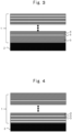
- FIG. 3 illustrates an example in which the thicknesses of metal films are made smaller in a surface portion
- FIG. 4 illustrates an example in which the thicknesses of metal films are made smaller in a region near the substrate. From a viewpoint of the manufacturing process, it is desired to set the thicknesses of the individual metal films to be substantially equal as in FIG. 2 .
- the interface layer 5 is a layer in which the metal element (second metal element) of small cohesive energy is contained more than in the metal films 3 and 4. It is basically preferred from a manufacturing viewpoint to use, as the principal component of the interface layer 5, the same component as in the metal film 3 or 4.
- the large content of the metal element of small cohesive energy means to make a binding force of the interface layer 5 weaker than those of the metal films 3 and 4, and the weaker interface layer 5 produces an effect that changes a propagation direction of cracks, which occur at surfaces and inside at the time of wear, into a direction perpendicular to the lamination direction of the laminate (into an in-plane direction of the interface layer). By this change in the propagation direction of the cracks, the wear rate of the laminate can be reduced, and the wear resistance is improved.
- metal elements smaller in cohesive energy than Cr are alkali metals, alkaline earth metals, Sc, Mn, Fe, Co, Cu, Ag, Au, Zn, Cd, Hg, Al, Ga, In, Tl, Ge, Sn, Pb, Sb, Bi, Pr, Nd, Sm, Eu, Tb, Dy, Ho, Er, Tm, and Yb.
- the binding force of the interface layer 5 can be made weaker by a small addition amount.
- a metal element of 2.79 ⁇ or longer or 2.19 ⁇ or shorter based on the values of the nearest-neighbor distances described on P.28 in Reference 1 is pertinent as such a metal element.
- alkaline earth metals except for Be, alkali metals, Sc, Ag, Au, Cd, Hg, Al, In, Tl, Sn, Pb, Sb, Bi, Pr, Nd, Sm, Eu, Tb, Dy, Ho, Er, Tm, and Yb.
- the binding force of the interface layer 5 is desired to be as closer to those of the metal films 3 and 4 as possible although the former must be weaker than the latter.
- examples include Be, Mn, Fe, Co, Cu, Zn, Ga, and Ge if selected in a similar manner as mentioned above.
- the metal element of small cohesive energy is desired to be an element that has a high standard electrode potential and is noble compared to the metal element contained as a principal component in the metal films 3 and 4. It is therefore facilitated to have the metal element of small cohesive energy contained more in the interface film 5 than in the metal films 3 and 4. It is also possible to decrease the amount of the additive, which is needed to form the interface layer 5, to a plating solution.
- S a metalloid element
- S may be further contained in addition to the metal element of small cohesive energy.
- the further inclusion of S not only facilitates occurrence of slippage at the interlace layer 5 upon shearing, but also hardens and smoothens the metal films 3 and 4 and improves the wear resistance of the laminated film portion 1. Further, stress can be relaxed at the interface portion, because tensile stress inside the plating films can be reduced by the S contained. Accordingly, the occurrence of cracks is suppressed, and the wear resistance is improved.
- the thickness of the interface layer 5 is desired to be set at 100 nm or smaller. If the thickness is greater than this range, the characteristics of the interface layer 5, in addition to those of the metal films 3 and 4, significantly affect the characteristics of the laminated film portion 1. Such a great thickness of the interface layer 5 is therefore not preferred.
- the thickness of the interface layer 5 is particularly preferably 10 nm or smaller, and such a thickness can improve the wear resistance alone without substantially affecting the laminated film portion 1.
- treatment methods such as wet treatment (for example, electroplating) and dry treatment (for example, sputtering) can each be used, but electroplating is a preferred manner from a viewpoint of mass productivity.
- An electroplating solution for forming the laminated film portion 1 contains as a principal component a metal salt of at least one selected from Ni, Cr, Co, and W, and also contains a compound containing a metal element having smaller cohesive energy than these metal elements.
- the metal salt to be contained as a principal component in the plating solution for forming the metal films 3 and 4 no limitations are imposed except that hexavalent chromium is not contained, and a commonly-used salt such as a sulfide or a chloride can be used. Examples include nickel sulfate, nickel chloride, copper sulfate, copper chloride, cobalt sulfate, cobalt chloride, tungsten chloride, and the like, and they can also be used in combination.
- the metal element of small cohesive energy for forming the interface layer 5 include alkali metals, alkaline earth metals, Sc, Mn, Fe, Co, Cu, Ag, Au, Zn, Cd, Hg, Al, Ga, In, Tl, Ge, Sn, Pb, Sb, Bi, Pr, Nd, Sm, Eu, Tb, Dy, Ho, Er, Tm, and Yb.
- a metal salt, an organometal compound, or the like, which contains the metal element can be used.
- Examples of the form include chlorides, sulfides, and organometal compounds.
- the metal element of small cohesive energy is contained not only in the interface layer 5 but also in a trace amount in the metal films 3 and 4.
- the amount to be added to the plating solution can appropriately be selected in accordance with design conditions such as the content of the selected metal element in the metal films 3 and 4.
- illustrative are chlorides, sulfides, and organometal compounds containing alkaline earth metals except for Be, alkali metals, Sc, Ag, Au, Cd, Hg, Al, In, Tl, Sn, Pb, Sb, Bi, Pr, Nd, Sm, Eu, Tb, Dy, Ho, Er, Tm, and Yb.
- the binding force of the interface layer 5 is desired to be as close to those of the metal films 3 and 4 as possible although the former must be weaker than the latter.
- the metal films 3 and 4 containing Ni as a principal component for example, it is preferred to add a chloride, sulfite, or organometal compound that contains Be, Mn, Fe, Co, Cu, Zn, Ga, or Ge.
- the amounts of components can appropriately be adjusted because the amounts added to a plating solution do not turn out in their entirety to form the metal films 3 and 4 and the interface layer 5.
- Ni is used as a principal component of plating and Cu is used as a metal element of small cohesive energy, for example, the amount of Cu to be added to the plating solution may be 3/100000 or less of a Ni salt.
- the metal element of small cohesive energy is desirably nobler than the metal element contained as a principal component in the metal films 3 and 4. Taking this into consideration, the metal element of small cohesive energy is desirably selected, for example, from Cu, Sn, Zn, Mn, Bi, and In if the principal component of the plating is Ni. Cu is more preferred.
- a reducing agent, a complexing agent, a pH modifier, a supporting salt, and other additives can also be contained as general plating components.
- the principal component of the metal films 3 and 4 is Ni, for example, P or/and B components may desirably be contained in the metal films to increase the hardness.
- P or/and B components may desirably be contained in the metal films to increase the hardness.
- phosphonic acid as a phosphorus compound, boric acid as a boron compound, or the like can be used and contained as a principal component.
- particles of an oxide for example, TiO 2 or Al 2 O 3
- particles of a carbide SiC, diamond, B 4 C, WC, or Cr 3 C 2
- particles of BN, TiN, MoS 2 , ZnF, graphite, or the like can also be similarly contained and dispersed in the plating solution.
- a sulfur-containing organic compound which contains sulfur as a metalloid element, in addition to the metal element of small cohesive energy, in the plating solution.
- a known gloss agent such as saccharin, sodium laurylsulfate, allylsulfonic acid, or thiourea can be used. These additives are prone to adsorption on the surfaces of the metal films 3 and 4, so that the interface layer 5 can readily be formed.
- treatment methods such as wet treatment (for example, electroplating) and dry treatment (for example, sputtering) can each be used as the manufacturing process of the present invention for the laminate (the film forming process of the laminated film portion), but electroplating is a preferred manner from the viewpoint of mass productivity. Accordingly, a description will hereinafter be made about a process of manufacturing the laminate by electroplating.
- the number of layers of the metal films can appropriately be set according to the specifications of corrosion resistance, wear resistance, service life, and the like required for each part, component, or product to which the laminate is applied.
- the above-described steps 1 to 3 should therefore be performed repeatedly according to the numbers of the layers of the metal films 3 and 4 in the laminated film portion 1.
- the step 2 for forming the interface layer 5 and the annealing treatment step 6 are important in the above-described process.
- the step for forming the interface layer 5 can appropriately be selected insofar as an interface layer can be formed under conditions different from those for the plating treatment.
- the stop time of the plating treatment can be used for the step for forming the interface layer 5.
- a sufficient stop time of the plating treatment for example, 30 seconds or longer
- the precursor substance that will form the interface layer 5 adsorbs on the surface of the metal film 3, and the interface layer 5 can then be formed concurrently with the plating treatment step 3 of the metal film 4.
- the annealing temperature is preferably set at 300°C or lower. This is a finding obtained from the results of the diligent study by the present inventors.
- the setting of the annealing temperature at 300°C or lower enables control of the average crystallite size of a nickel alloy film at 8 nm or smaller.
- An annealing temperature of higher than 300°C is prone to make the crystallite of the nickel alloy film coarse, so that the hardness of the laminated film portion 1 is reduced.
- the annealing treatment time is not particularly limited but may preferably be, for example, one hour or longer.
- the current density and the treatment time may appropriately be adjusted according to the desired film thickness, and from a viewpoint of making equal the thickness of each film, are preferably set under the same conditions.
- Impurity removal steps such as degreasing and pickling may also be performed as pretreatments for the substrate 2 before the plating treatment step 1 of the metal film 3 as needed.
- an adhesive layer forming step (for example, strike plating or the like) may also be performed to improve the adhesiveness of the laminated film portion 1.
- the manufacturing process of the present invention for the laminate forms a plurality of layers of metal films under the same electrolysis conditions by using a single plating bath, and therefore has an advantage that it is simple and convenient and is high in productivity (in other words, is low in cost).
- the shape of the substrate 2 is not particularly limited, and the laminate can be applied to a part or component of any shape (for example, block, flat plate, curved plate, cylinder, prism). If the films are formed by electroplating, however, the film thickness may vary with the place due to the effect of a current distribution depending on the shape of the part or component (the shape of the substrate 2). It is therefore preferred to measure the effect of a current distribution beforehand through an analysis and an actual measurement, and to perform electroplating under conditions that allow suppression of plating placedependent variations in film thickness, by arranging a shielding plate or the like between the workpiece and a counter electrode as needed, for example.
- Example 1 Ni (cohesive energy: 428 kJ/mol) was selected for metal films 35 and 45, Cu (cohesive energy: 336 kJ/mol) was selected as a metal element of small cohesive energy for an interface layer 55, and a structure model as illustrated in FIG. 5 was created. To that structure model, a shear that would act at the time of a wear test was applied at a deformation rate of 10 m/s.
- Comparative Example 1 is presented in FIG. 6 .
- Ni was selected for metal films 36 and 46 as in Example 1, and W (cohesive energy: 859 kJ/mol), which is a metal element greater in cohesive energy than Ni, was selected for an interface layer 56.
- W cohesive energy: 859 kJ/mol
- a structure model as illustrated in FIG. 6 was created. To the structure model, a shear was similarly applied at a deformation rate of 10 m/s.
- Example 1 Cu was selected as a metal element of small cohesive energy for use in the interface layer 5.
- Example 2 a study was also conducted on other examples of the interface layer 5, from which similar effects are obtained.
- a metal element other than Cu exists, a similar phenomenon is considered to occur in principle if the cohesive energy of the interface layer 5 is smaller than those of the metal films 3 and 4.
- the metal element that exists in the interface layer 5 is by no means limited to Cu, and no restrictions are imposed whatsoever insofar as metal elements of small cohesive energy are concerned.
- the results of this study are hence considered to be also realized with metal elements other than Cu, for example, with metal elements such as alkali metals, alkaline earth metals, Sc, Mn, Fe, Co, Ag, Au, Zn, Cd, Hg, Al, Ga, In, Tl, Ge, Sn, Pb, Sb, Bi, Pr, Nd, Sm, Eu, Tb, Dy, Ho, Er, Tm, and Yb.
- Example 1 the simple metal was studied as a metal element to be applied to the interface layer 5.
- Example 2 a further study was conducted on a case in which a plurality of elements existed in combination in the interface layer 5.
- a structure model was created in which Ni was selected for metal films 37 and 47 as in Example 1, and S (cohesive energy: 275 kJ/mol), a metalloid element, additionally existed in an interface layer 57 in combination with Cu, a metal element of small cohesive energy.
- S is selected because S is such an element that, in addition to its small cohesive energy, when a plating process is assumed, an S-containing compound is widely used as a gloss agent in general and is easy to introduce into a plating solution and plating films, and there is a possibility that it becomes essential to add such an S-containing compound in a viewpoint other than wear resistance.
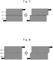
- Example 1 When a shear was applied as in Example 1, it was found that, as illustrated in the right diagram of FIG. 7 , slip deformation occurred in the interface layer 57 and an internal break was suppressed. This is considered to be attributable to the occurrence of substantially no tensile deformation in the metal films 37 and 47 and the occurrence of a shear in the interface layer 57, because upon shearing, the shear stress (172 MPa) at which the shear occurred in the interface layer 57 was greater than the tensile stress (57.3 MPa) inside the Ni layers, the metal films 37 and 47.
- Example 3 a structure model of FIG. 8 was created in which Ni was selected for metal films 38 and 48 as in Example 1, and Cu and S of small cohesive energy additionally existed in an interface layer 58 in combination with Ni, the same metal element as that in the metal films 38 and 48.
- a shear was applied as in Example 1, it was found that, as illustrated in FIG. 8 , slip deformation occurred and an internal break was suppressed.
- the element, which makes up the interface layer 5 is not needed to consist of only an element completely different from that of the metal films 3 and 4 as presented in Examples 1 and 2, and similar advantageous effects are available if an element of small cohesive energy is scattered about in the layer.
- the formation of an interface layer having a larger shear stress than metal films can be achieved by making the content ratio of an element of small cohesive energy higher in the interface layer 5 than in the metal film 3 or 4.
- each laminated film portion As a substrate for forming each laminated film portion 1, SUS 303 material (50 mm ⁇ 70 mm ⁇ 3 mm) finished at a surface thereof to an arithmetic mean roughness Ra ⁇ 0.05 um by mechanical polishing was used. To form the metal films 3 and 4, an Ni-P electroplating solution based on Watts bath and presented in Table 1 was used. As additives for forming the interface layer 5, the compounds presented in Table 1 were added into the electroplating solution. As metal elements of small cohesive energy, Cu, Sn, Zn, Mn, Bi, and In were studied. Saccharine was used as an S source for improving wear resistance and gloss properties. As Comparative Examples, plating solutions free of an additive or additives for not forming the interface layer 5 were also prepared.
- a manufacturing process of each laminate was performed following the above-mentioned flow. Specifically, impurity removal steps for degreasing and pickling were first performed as pretreatments for the substrate. Further, oxide films on the substate were removed, and strike plating of Ni was performed to provide the resulting plating film with improved adhesiveness.
- electroplating treatment conditions were set in such a manner that each film had a thickness of 500 nm and the number of layers was set to 20 (the overall thickness of plating layers was 10 um).
- electrolysis conditions for the plating treatment steps the plating treatment was conducted at a constant current by using an Ni plate as a counter electrode.
- the formation was designed to be performed by stopping the electrolysis, and the stop time was set to 30 seconds.
- Those formed with a single-layer film instead of a laminated film portion were also prepared as comparisons.
- annealing treatment was further performed on the film or films of each laminate so prepared.
- the annealing temperature was set to 300°C, and the holding time was set to 2 h.
- Example 4 in which the interface layers 5 were formed, on the other hand, the films were not delaminated after the wear resistance test, so that it was confirmed that the wear resistance was improved over those in Comparative Examples 2 to 4. These results are correlated with the results of the simulation in Example 1, so that, in Example 4, the wear resistance is considered to have been improved owing to suppression of internal propagation of cracks occurred in the films.
- Example 5 When the laminate of Example 5 was analyzed by XRD, a (200) peak also appeared besides a (111) peak of Ni and the crystallite size was 6 nm in Example 5, although in Comparative Examples 2 and 3, only the (111) peak appeared and the crystallite size was 8 nm. It has therefore been realized that the orientation plane of a laminate is desirably in (100) orientation in order to improve the wear resistance.
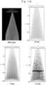
- FIG. 9 shows a cross-sectional SEM image of Example 5.
- the prepared films were formed from the laminated film portion. It has also been confirmed by a SIMS analysis that more S existed locally in the interfaces of plural layers than that contained in the metal films.
- concentrations of elements contained in the films were analyzed by XRF, on the other hand, they were found as follows: Ni: 93.36, P: 6.56, S: 0.07, and Cu: 0.01 in at%.
- FIG. 10 shows atom maps of an interface portion as analyzed by an atom probe.
- the principal components of the interface portion were Ni and P, but Cu, a metal element of small cohesive energy, locally existed at 0.04 at% in the interface.
- the interface layer existed with a thickness of 10 nm or smaller.
- Concerning S on the other hand, it was unable to ascertain its distribution as its peak overlaps that of Ni.
- Cu was selected as a metal element of small cohesive energy, and a study was conducted about desired addition amounts of Cu. The study was conducted by the same method as that described in Examples 4 to 10 except that the plating solution was changed.
- Example 11 The results of Examples 11 to 14 are presented in Table 2. Assuming that the wear resistance of Example 11, in which copper sulfate pentahydrate was added at 0.002 g/L without addition of saccharin, was 100, the respective Examples were compared in wear resistance. [Table 2] Raw material Compound (g/L) Ex. 11 Ex. 12 Ex. 13 Ex.
- a plating solution desirably contains Cu at 0.02 g/L or lower, more desirably, 0.01 g/L or lower, as a concentration of copper sulfate pentahydrate.
- test pieces were each embedded in a resin, sliced, and observed at a cross-section.
- the respective cross-sectional SEM images are shown in FIG. 11 and FIG. 12 .
- Example 15 which had a laminated film portion 12 with the interface layers 5 abundantly containing the metal element of small cohesive energy
- Comparative Example 5 which had a single-layer film 11 free of any interface layer 5.
Landscapes
- Chemical & Material Sciences (AREA)
- Organic Chemistry (AREA)
- Engineering & Computer Science (AREA)
- Chemical Kinetics & Catalysis (AREA)
- Materials Engineering (AREA)
- Metallurgy (AREA)
- Electrochemistry (AREA)
- General Chemical & Material Sciences (AREA)
- Mechanical Engineering (AREA)
- Crystallography & Structural Chemistry (AREA)
- Laminated Bodies (AREA)
- Electroplating Methods And Accessories (AREA)
- Electroplating And Plating Baths Therefor (AREA)
Abstract
Description
- The present invention relates to a laminate with a plurality of layers of films laminated on a substrate, a metal plating solution, and a manufacturing process of the laminate.
- In a variety of equipment, there is an increasing tendency in recent years toward their use under environments severer than before. Examples include piping and pumps used in offshore wind power generation facilities and sea water desalination plants, automotive vehicles and construction equipment in areas where a great deal of snow melting agent or the like is sprinkled and salt damage is severe, and so on.
- In metal parts and components employed in such equipment, degradation is prone to progress at their surfaces due to combined factors of corrosion, wear, and the like, leading to potential concerns for increased frequency of equipment maintenance and decreased equipment service life.
- Under the current circumstances, surface treatment by hexavalent chromium plating excellent in corrosion resistance and wear resistance is often adopted for metal parts and components the degradation of which is prone to progress due to the above-mentioned combined factors.
- Hexavalent chromium is however designated as a substance of very high environmental concern in restrictions on environment and restrictions on drainage such as the REACH regulations (Regulation concerning the Registration, Evaluation, Authorization and Restrictions of Chemicals, establishing a European Chemical Agency), and a reduction of its employment is desired worldwide. Given such a background, a variety of surface treatment techniques has been proposed as plating techniques that replace hexavalent chromium plating.
- For example,
Patent Document 1 discloses a multilayered Ni alloy plating film or the like, in which a plurality of Ni alloy plating films is formed on a surface of a workpiece, the Ni alloy plating films in the individual layers contain an element, which is selected from P, B, or S, at different concentrations, and as a mutual potential relation between each two adjacent Ni alloy plating films, the outer Ni alloy plating film is disposed in a relation with its inner Ni alloy plating film in such a manner that the former is baser by 30 mV or more than the latter. - Further,
Patent Document 2 discloses a film laminate with a plurality of layers of sulfur-containing nickel alloy films laminated on a substrate, in which differences in Ni concentration among the individual films are within one mass%, and S-concentrated layers are arranged between the respective films. It is also disclosed that pitting corrosion is changed into a direction horizontal to the film thickness under a sacrificial corrosion protection effect of the S-concentrated layers. -
- Patent Document 1:
JP S63-105990 A - Patent Document 2:
WO 2019/064672 A - Due to an expansion of the application field of metal parts and components and increasing severity of environments, however, further improvements are desired in wear resistance, especially, sliding wear resistance, adhesive wear resistance, and the like.
- The present invention therefore has as an object thereof the provision of a laminate excellent in corrosion resistance and wear resistance without use of hexavalent chromium, and a manufacturing process of the laminate.
- To solve the above-described problem, a laminate according to the present invention includes a substrate and a laminated film portion with metal films laminated in two or more layers. The laminate has an interface layer between each two adjacent ones of the metal films. The laminated film portion contains a first metal element as a principal component, the first metal element being at least one element of Ni, Cr, Co, and W, and a second metal element that is a metal element of smaller cohesive energy than that of the first metal element. The second metal element contained in the interface layer is at a content ratio higher than that of the second metal element contained in each of the adjacent metal films.
- According to the present invention, a laminate that is free of hexavalent chromium and excellent in corrosion resistance and wear resistance can be provided.
-
-
FIG. 1 is a schematic cross-sectional view illustrating an example of a laminate according to the present invention. -
FIG. 2 is a schematic cross-sectional view illustrating another example of the laminate according to the present invention. -
FIG. 3 is a schematic cross-sectional view illustrating a further example of the laminate according to the present invention. -
FIG. 4 is a schematic cross-sectional view illustrating a still further example of the laminate according to the present invention. -
FIG. 5 is a molecular dynamics simulation according to an embodiment of the present invention. -
FIG. 6 is a molecular dynamics simulation according to a comparative embodiment of the present invention. -
FIG. 7 is a molecular dynamics simulation according to another embodiment of the present invention. -
FIG. 8 is a molecular dynamics simulation according to a further embodiment of the present invention. -
FIG. 9 is a cross-sectional SEM image according to a still further embodiment of the present invention. -
FIG. 10 shows atom maps by an atom probe according to the still further embodiment of the present invention. -
FIG. 11 is a cross-sectional SEM image after a wear resistance test according to another comparative embodiment of the present invention. -
FIG. 12 is a cross-sectional SEM image after a wear resistance test according to a yet further embodiment of the present invention. - Using the drawings, some examples of a film structure will hereinafter be described in detail as embodiments of the present invention. It is however to be noted that the present invention is not limited to the embodiments included herein and can be appropriately combined with known techniques or improved or otherwise modified based on known techniques without departing from the technical concept of the present invention.
-
FIG. 1 is a schematic cross-sectional view illustrating an example of the laminate according to the present invention. As illustrated inFIG. 1 , the laminate includes a laminatedfilm portion 1 formed on a surface of asubstrate 2. In this example, the laminatedfilm portion 1 has ametal film 3 and anothermetal film 4 laminated in two layers. - The
substrate 2 is not particularly limited, and an appropriate selection can be made depending on the use of the laminate. For example, carbon steel, low alloy steel, stainless steel, copper, aluminum, their alloys, and the like can appropriately be used. Preferably, however, a metal element of small cohesive energy may be contained in the substrate (for example, a case in which Cu or the like is contained in the substrate as will be mentioned below). This is because, if a plating process is applied to a manufacturing process of the laminate, dissolution of the metal element of small cohesive energy takes place from the substrate into a plating solution, thereby obviating any deliberate incorporation of the metal element of small cohesive energy as an additive in the plating solution. If this is the case, the metal element of small cohesive energy may be contained as a component in the substrate, or the substrate may include plural materials (for example, a thin film is formed on a stainless steel substrate). As to its contained form, no particular limitations should be imposed accordingly. - A characteristic feature of the laminate of the present invention is that, in the laminated
film portion 1, aninterface layer 5 is provided between theadjacent metal films 3 and 4 (in an interface region). Themetal films metal films interface layer 5 than in theadjacent metal films - Now, the term "cohesive energy" means energy (cohesive energy) required to separate atoms of a substance, which exists in an aggregation state, apart from each other to infinity. The present inventors lately conducted a study using the value of energy that is required to form separated neutral atoms in their ground state from a solid at 0K and 1 atm and that is published at p.70 in Kittel, Introduction to Solid State Physics, Vol. 1, 5th ed., Maruzen Co., Ltd., 1978 (Reference 1). Lattice constants (nearest-neighbor distances) and the like are also published in ibid. p.28.
- The
metal films metal films film portion 1. - The Ni-based
metal films - For the purpose of similarly achieving hardening, the
metal films metal films - For the purpose of forming smooth surfaces, the Ni-based
metal films metal films - Thicknesses of the
metal films laminated film portion 1 in principle, and hence is not preferred. If greater than 1000 nm, on the other hand, the effect that improves the wear resistance is hardly produced. The wear resistance can therefore be improved by setting the thicknesses of theindividual metal films metal films - In addition, the
metal films FIG. 2 , and as an alternative, one or more thicker metal films and/or one or more thinner metal films may be appropriately included in combination.FIG. 3 illustrates an example in which the thicknesses of metal films are made smaller in a surface portion, whileFIG. 4 illustrates an example in which the thicknesses of metal films are made smaller in a region near the substrate. From a viewpoint of the manufacturing process, it is desired to set the thicknesses of the individual metal films to be substantially equal as inFIG. 2 . - As mentioned above, the
interface layer 5 is a layer in which the metal element (second metal element) of small cohesive energy is contained more than in themetal films interface layer 5, the same component as in themetal film interface layer 5 weaker than those of themetal films weaker interface layer 5 produces an effect that changes a propagation direction of cracks, which occur at surfaces and inside at the time of wear, into a direction perpendicular to the lamination direction of the laminate (into an in-plane direction of the interface layer). By this change in the propagation direction of the cracks, the wear rate of the laminate can be reduced, and the wear resistance is improved. - The metal element (second metal element) that has small cohesive energy and constitutes the
interface layer 5 can be selected from various elements while taking into account the readiness of formation and the like in the manufacture. Among Ni, Cr, Co, and W (first metal elements) which can each be contained as a principal component in themetal films - As to how much the metal element of small cohesive energy should be used relative to the above-mentioned metal element contained as a principal component in the
metal films - For example, if it is desired to facilitate shearing in the
interface layer 5 through a reduction in the binding force of theinterface layer 5 by its addition in a small amount, it is desired, in addition to selection of a metal element of as small the cohesive energy as possible, to select such a metal element as producing a lattice mismatch of greater than 12% with themetal films interface layer 5 can be made weaker by a small addition amount. In the case of themetal films Reference 1 is pertinent as such a metal element. Illustrative are alkaline earth metals except for Be, alkali metals, Sc, Ag, Au, Cd, Hg, Al, In, Tl, Sn, Pb, Sb, Bi, Pr, Nd, Sm, Eu, Tb, Dy, Ho, Er, Tm, and Yb. - On the other hand, if addition can be made in a certain amount, for example, the binding force of the
interface layer 5 is desired to be as closer to those of themetal films metal films metal films metal films - When the
laminated film portion 1 is formed by a plating process, the metal element of small cohesive energy is desired to be an element that has a high standard electrode potential and is noble compared to the metal element contained as a principal component in themetal films interface film 5 than in themetal films interface layer 5, to a plating solution. - Taking the foregoing into consideration, it is desired to contain, as the metal element of small cohesive energy, a metal element selected, for example, from Cu, Sn, Zn, Ag, Mn, Bi, In, or Sb. Cu is more preferred.
- In the
interface layer 5, S, a metalloid element, may be further contained in addition to the metal element of small cohesive energy. The further inclusion of S not only facilitates occurrence of slippage at theinterlace layer 5 upon shearing, but also hardens and smoothens themetal films laminated film portion 1. Further, stress can be relaxed at the interface portion, because tensile stress inside the plating films can be reduced by the S contained. Accordingly, the occurrence of cracks is suppressed, and the wear resistance is improved. - The thickness of the
interface layer 5 is desired to be set at 100 nm or smaller. If the thickness is greater than this range, the characteristics of theinterface layer 5, in addition to those of themetal films laminated film portion 1. Such a great thickness of theinterface layer 5 is therefore not preferred. The thickness of theinterface layer 5 is particularly preferably 10 nm or smaller, and such a thickness can improve the wear resistance alone without substantially affecting thelaminated film portion 1. - A description will be made about a plating solution for the manufacture of the laminate according to the present invention. As the manufacturing process of the present invention for the laminate (a film forming process of the laminated film portion), treatment methods such as wet treatment (for example, electroplating) and dry treatment (for example, sputtering) can each be used, but electroplating is a preferred manner from a viewpoint of mass productivity.
- An electroplating solution for forming the
laminated film portion 1 contains as a principal component a metal salt of at least one selected from Ni, Cr, Co, and W, and also contains a compound containing a metal element having smaller cohesive energy than these metal elements. - As the metal salt to be contained as a principal component in the plating solution for forming the
metal films - As the metal element of small cohesive energy for forming the
interface layer 5, usable examples include alkali metals, alkaline earth metals, Sc, Mn, Fe, Co, Cu, Ag, Au, Zn, Cd, Hg, Al, Ga, In, Tl, Ge, Sn, Pb, Sb, Bi, Pr, Nd, Sm, Eu, Tb, Dy, Ho, Er, Tm, and Yb. - No particular limitations are imposed on the form of the compound which contains the metal element of small cohesive energy and is to be contained in the plating solution. A metal salt, an organometal compound, or the like, which contains the metal element, can be used. Examples of the form include chlorides, sulfides, and organometal compounds.
- It is to be noted that, by the addition of such a compound to the plating solution, the metal element of small cohesive energy is contained not only in the
interface layer 5 but also in a trace amount in themetal films - As to how much the metal element of small cohesive energy should be used relative to the above-mentioned metal element contained as a principal component in the
metal films metal films - If it is desired to facilitate shearing in the
interface layer 5 by reducing the binding force of theinterface layer 5 through the addition in a small amount, it is desired to select such a metal element as producing a lattice mismatch of greater than 12% with themetal films metal films - On the other hand, if a certain amount can be introduced as an addition amount, for example, the binding force of the
interface layer 5 is desired to be as close to those of themetal films metal films metal films metal films - If the laminate of the invention of this application is formed by a plating process, the amounts of components can appropriately be adjusted because the amounts added to a plating solution do not turn out in their entirety to form the
metal films interface layer 5. If Ni is used as a principal component of plating and Cu is used as a metal element of small cohesive energy, for example, the amount of Cu to be added to the plating solution may be 3/100000 or less of a Ni salt. - When the
laminated film portion 1 is formed by a plating process, the metal element of small cohesive energy is desirably nobler than the metal element contained as a principal component in themetal films - In the plating solution, a reducing agent, a complexing agent, a pH modifier, a supporting salt, and other additives can also be contained as general plating components. If the principal component of the
metal films - For the purpose of similarly achieving hardening with use of an additive, it is also possible to have particles of an oxide (for example, TiO2 or Al2O3) or particles of a carbide (SiC, diamond, B4C, WC, or Cr3C2) contained and dispersed in the plating solution. In addition, for the purpose of increasing lubricity, particles of BN, TiN, MoS2, ZnF, graphite, or the like can also be similarly contained and dispersed in the plating solution.
- For the purpose of improving slippage of the
interface layer 5 upon shearing and for the purpose of hardening and smoothening themetal films metal films interface layer 5 can readily be formed. - It is to be noted that the concentrations of various components in the electroplating solution can adequately be adjusted.
- A description will be made about the manufacturing process according to the present invention for the laminate. As mentioned above, treatment methods such as wet treatment (for example, electroplating) and dry treatment (for example, sputtering) can each be used as the manufacturing process of the present invention for the laminate (the film forming process of the laminated film portion), but electroplating is a preferred manner from the viewpoint of mass productivity. Accordingly, a description will hereinafter be made about a process of manufacturing the laminate by electroplating.
- An electroplating process as an example of the manufacturing process according to the present invention for the laminate will be presented hereinafter.
- 1. Plating treatment step of the
metal film 3 - 2. Treatment step for forming the
interface layer 5 - 3. Plating treatment step of the
metal film 4 - 4. Rinsing step
- 5. Drying step
- 6. Annealing treatment step
- The description has been made about the
laminated film portion 1 in which the two layers of themetal films steps 1 to 3 should therefore be performed repeatedly according to the numbers of the layers of themetal films laminated film portion 1. - To produce excellent wear resistance at the
laminated film portion 1 of the laminate of the present invention, thestep 2 for forming theinterface layer 5 and the annealing treatment step 6 are important in the above-described process. - The step for forming the
interface layer 5 can appropriately be selected insofar as an interface layer can be formed under conditions different from those for the plating treatment. For example, by adding a compound (interface layer precursor substance), which adsorbs on the metal films, to the plating solution under plating treatment stop conditions, the stop time of the plating treatment can be used for the step for forming theinterface layer 5. Specifically, by setting a sufficient stop time of the plating treatment (for example, 30 seconds or longer) with the substrate kept immersed in the plating solution, the precursor substance that will form theinterface layer 5 adsorbs on the surface of themetal film 3, and theinterface layer 5 can then be formed concurrently with theplating treatment step 3 of themetal film 4. It is also a characteristic feature that no rinsing is carried out between the stop after the plating treatment, which is the formation treatment of theinterface layer 5, and the plating treatment step of themetal film 4. If rinsing were carried out, the substance adsorbed on the surface to form theinterface layer 5 would flow off, and therefore, it would be unable to form theinterface layer 5. - In the annealing treatment step, the annealing temperature is preferably set at 300°C or lower. This is a finding obtained from the results of the diligent study by the present inventors. The setting of the annealing temperature at 300°C or lower enables control of the average crystallite size of a nickel alloy film at 8 nm or smaller. An annealing temperature of higher than 300°C is prone to make the crystallite of the nickel alloy film coarse, so that the hardness of the
laminated film portion 1 is reduced. The annealing treatment time is not particularly limited but may preferably be, for example, one hour or longer. - It is to be noted that, as electrolysis conditions for the
plating treatment step 1 of themetal film 3 and theplating treatment step 3 of themetal film 4, the current density and the treatment time may appropriately be adjusted according to the desired film thickness, and from a viewpoint of making equal the thickness of each film, are preferably set under the same conditions. - Impurity removal steps such as degreasing and pickling may also be performed as pretreatments for the
substrate 2 before theplating treatment step 1 of themetal film 3 as needed. Further, an adhesive layer forming step (for example, strike plating or the like) may also be performed to improve the adhesiveness of thelaminated film portion 1. - As described above, the manufacturing process of the present invention for the laminate forms a plurality of layers of metal films under the same electrolysis conditions by using a single plating bath, and therefore has an advantage that it is simple and convenient and is high in productivity (in other words, is low in cost).
- In the present invention, the shape of the substrate 2 (in other words, the shape of the laminate) is not particularly limited, and the laminate can be applied to a part or component of any shape (for example, block, flat plate, curved plate, cylinder, prism). If the films are formed by electroplating, however, the film thickness may vary with the place due to the effect of a current distribution depending on the shape of the part or component (the shape of the substrate 2). It is therefore preferred to measure the effect of a current distribution beforehand through an analysis and an actual measurement, and to perform electroplating under conditions that allow suppression of plating placedependent variations in film thickness, by arranging a shielding plate or the like between the workpiece and a counter electrode as needed, for example.
- A detailed description will hereinafter be made using Examples. However, the present invention is not limited to the description of the Examples included herein, and the Examples may be combined appropriately.
- To demonstrate advantageous effects of the present invention, molecular dynamics simulations were performed on structure models, and deformation behaviors of laminated film portions due to correlations in cohesive energy were evaluated. In this Example, a study was conducted using a method such as that disclosed, for example, in R. Car and M. Parrinello, Phys. Rev. Lett., 50, 2471. (1985) (Reference 2). As illustrated in
FIG. 5 to FIG. 8 , a shear force was applied tometal films Reference 3. - In Example 1, Ni (cohesive energy: 428 kJ/mol) was selected for
metal films interface layer 55, and a structure model as illustrated inFIG. 5 was created. To that structure model, a shear that would act at the time of a wear test was applied at a deformation rate of 10 m/s. - As a result, it was found that the Cu layer and the interface portions between Cu and Ni underwent slip deformation and an internal break was suppressed. This is considered to be attributable to the occurrence of substantially no tensile deformation in the
metal films interface layer 55 because, upon shearing, the shear stress (168 MPa) at which a shear occurred in theinterface layer 55 was greater than the tensile stress (98.7 MPa) inside the Ni layers that form themetal films interface layer 55 if a metal element of small cohesive energy exists in theinterface layer 55. - On the other hand, Comparative Example 1 is presented in
FIG. 6 . In Comparative Example 1, Ni was selected formetal films 36 and 46 as in Example 1, and W (cohesive energy: 859 kJ/mol), which is a metal element greater in cohesive energy than Ni, was selected for aninterface layer 56. Similarly to Example 1, a structure model as illustrated inFIG. 6 was created. To the structure model, a shear was similarly applied at a deformation rate of 10 m/s. - As a result, it was found that cracks occurred in the metal film 36 made from Ni, and the cracks so occurred then ran through the
interface layer 56 and propagated into themetal film 46. This is considered to be a result of preferential occurrence of an internal break rather than shear deformation, because the tensile stress (216 MPa) occurred inside the Ni layers as themetal films 36 and 46 upon shearing was greater than the shear stress (187 MPa) at the interfaces. It has therefore been found that, with theinterface layer 56 using the metal element of large cohesive energy, no improvement can be expected in wear resistance because cracks run through theinterface layer 56 and propagate into the metal film at the time of a wear test. - From the above results, it has been realized that, when a metal element of smaller cohesive energy than those of the
adjacent metal films interface layer 5, internal propagation of cracks is suppressed at the time of a wear test on the metal films, and the wear resistance is improved. - It is to be noted that, in the case of a film (Comparative Example 2) of a similar thickness as in Example 1 and Comparative Example 1 without the
interface layer 5, similar results as in Comparative Example 1 are inferred to be obtained as theshearable interface layer 5 does not exist, although no calculation was made. - In Example 1, Cu was selected as a metal element of small cohesive energy for use in the
interface layer 5. In addition, a study was also conducted on other examples of theinterface layer 5, from which similar effects are obtained. When a metal element other than Cu exists, a similar phenomenon is considered to occur in principle if the cohesive energy of theinterface layer 5 is smaller than those of themetal films - Therefore, the metal element that exists in the
interface layer 5 is by no means limited to Cu, and no restrictions are imposed whatsoever insofar as metal elements of small cohesive energy are concerned. The results of this study are hence considered to be also realized with metal elements other than Cu, for example, with metal elements such as alkali metals, alkaline earth metals, Sc, Mn, Fe, Co, Ag, Au, Zn, Cd, Hg, Al, Ga, In, Tl, Ge, Sn, Pb, Sb, Bi, Pr, Nd, Sm, Eu, Tb, Dy, Ho, Er, Tm, and Yb. - In Example 1 and Comparative Example 1, the simple metal was studied as a metal element to be applied to the
interface layer 5. As Example 2, a further study was conducted on a case in which a plurality of elements existed in combination in theinterface layer 5. - As illustrated in
FIG. 7 , a structure model was created in which Ni was selected formetal films interface layer 57 in combination with Cu, a metal element of small cohesive energy. Here, S is selected because S is such an element that, in addition to its small cohesive energy, when a plating process is assumed, an S-containing compound is widely used as a gloss agent in general and is easy to introduce into a plating solution and plating films, and there is a possibility that it becomes essential to add such an S-containing compound in a viewpoint other than wear resistance. - When a shear was applied as in Example 1, it was found that, as illustrated in the right diagram of
FIG. 7 , slip deformation occurred in theinterface layer 57 and an internal break was suppressed. This is considered to be attributable to the occurrence of substantially no tensile deformation in themetal films interface layer 57, because upon shearing, the shear stress (172 MPa) at which the shear occurred in theinterface layer 57 was greater than the tensile stress (57.3 MPa) inside the Ni layers, themetal films - It has therefore been found that, even when S, a metalloid element, exists in combination in addition to a metal element of small cohesive energy, similar advantageous effects are available.
- In Example 3, a structure model of
FIG. 8 was created in which Ni was selected formetal films interface layer 58 in combination with Ni, the same metal element as that in themetal films FIG. 8 , slip deformation occurred and an internal break was suppressed. This is considered to be attributable to the occurrence of substantially no tensile deformation in themetal films interface layer 58, because upon shearing, the shear stress (155 MPa) at which the shear occurred in theinterface layer 58 was greater than the tensile stress (116 MPa) inside the Ni layers, themetal films - It has hence been realized that the element, which makes up the
interface layer 5, is not needed to consist of only an element completely different from that of themetal films interface layer 5 than in themetal film - As a substrate for forming each
laminated film portion 1, SUS 303 material (50 mm × 70 mm × 3 mm) finished at a surface thereof to an arithmetic mean roughness Ra < 0.05 um by mechanical polishing was used. To form themetal films interface layer 5, the compounds presented in Table 1 were added into the electroplating solution. As metal elements of small cohesive energy, Cu, Sn, Zn, Mn, Bi, and In were studied. Saccharine was used as an S source for improving wear resistance and gloss properties. As Comparative Examples, plating solutions free of an additive or additives for not forming theinterface layer 5 were also prepared. - A manufacturing process of each laminate was performed following the above-mentioned flow. Specifically, impurity removal steps for degreasing and pickling were first performed as pretreatments for the substrate. Further, oxide films on the substate were removed, and strike plating of Ni was performed to provide the resulting plating film with improved adhesiveness.
- For the plating treatment steps of metal films, electroplating treatment conditions were set in such a manner that each film had a thickness of 500 nm and the number of layers was set to 20 (the overall thickness of plating layers was 10 um). As electrolysis conditions for the plating treatment steps, the plating treatment was conducted at a constant current by using an Ni plate as a counter electrode. In a treatment step for forming the
interface layer 5, the formation was designed to be performed by stopping the electrolysis, and the stop time was set to 30 seconds. Those formed with a single-layer film instead of a laminated film portion were also prepared as comparisons. On the film or films of each laminate so prepared, annealing treatment was further performed. In the annealing treatment step, the annealing temperature was set to 300°C, and the holding time was set to 2 h. - Identification and crystallite size measurement of crystal phases in each laminate so prepared were performed using wide-angle X-ray diffractometry. Evaluation of wear resistance of each prepared laminate was conducted using a reciprocating sliding test machine. In the evaluation of wear resistance, after a mating material (bearing steel SUJ2; 10 mm dia.) was reciprocally slid over 0.04 m under a load of 9.8 N and at a rate of 0.1 m/s under non-lubrication conditions, an average value of wear marks of a specimen was measured through measurement of steps at several points. Each specimen with the film or films cracked and delaminated by the wear resistance test is indicated as "×" in Table 1, whereas each specimen with the film or films remained in a worn-down state without delamination by the wear resistance test is indicated as "o" in Table 1.
- The compositions of the used plating solutions, the plural-layer/single-layer structures of the plating films, and the evaluation results of wear resistance in Examples 4 to 10 and Comparative Examples 2 to 4 are presented in Table 1.
[Table 1] Raw material compound (g/L) Comp. Ex. 2 Comp. Ex. 3 Comp. Ex. 4 Ex. 4 Ex. 5 Ex. 6 Ex. 7 Ex. 8 Ex. 9 Ex. 10 Basic composition of solution Nickel sulfate hexahydrate 262.9 262.9 262.9 262.9 262.9 262.9 262.9 262.9 262.9 262.9 Nickel chloride hexahydrate 27.4 27.4 27.4 27.4 27.4 27.4 27.4 27.4 27.4 27.4 Phosphonic acid 32 . 8 32.8 32.8 32.8 32 . 8 32 . 8 32 . 8 32.8 32.8 32.8 Trisodium citrate dihydrate 147.05 147.05 147.05 147.05 147.05 147.05 147.05 147.05 147.05 147.05 Additive Saccharin 0 0 0 0 2 2 2 2 2 2 Copper sulfate pentahydrate 0 0 0.002 0.002 0.002 0 0 0 0 0 Tin sulfate 0 0 0 0 0 0.002 0 0 0 0 Zinc sulfate heptahydrate 0 0 0 0 0 0 0.002 0 0 0 Manganese sulfate 0 0 0 0 0 0 0 0.002 0 0 Bismuth sulfate 0 0 0 0 0 0 0 0 0.002 0 Indium sulfate 0 0 0 0 0 0 0 0 0 0.002 Characteristics of film structure Layer structure of plating layer (s) Single layer 20 layers Single layer 20 layers 20 layers 20 layers 20 layers 20 layers 20 layers 20 layers Evaluation of wear resistance × × × ○ ○ ○ ○ ○ ○ ○ - Interface layer components in the Examples, in which Cu was added, were confirmed. The component proportions in terms of at% were Cu: 0.03 at%, Ni: 93.4 at%, P: 6.5 at%, and S: 0.05 to 0.07 at%. On the other hand, the content of the Cu component in each plating solution was 2.3 mg/L in copper sulfate pentahydrate conversion.
- As indicated in Comparative Examples 2 and 3 of Table 1, with the plating solutions in which none of the additives for forming the
interface layer 5 existed, the metal film or films in both the single layer and the 20 layers were delaminated due to the introduction and propagation of cracks in the wear resistance tests. In Comparative Example 4 in which theinterface layer 5 was not formed though Cu, a metal element of small cohesive energy, was contained, the metal film was also delaminated similarly. - In Example 4 in which the interface layers 5 were formed, on the other hand, the films were not delaminated after the wear resistance test, so that it was confirmed that the wear resistance was improved over those in Comparative Examples 2 to 4. These results are correlated with the results of the simulation in Example 1, so that, in Example 4, the wear resistance is considered to have been improved owing to suppression of internal propagation of cracks occurred in the films.
- As also presented in Table 1, the wear resistance was similarly improved even in each case in which S, a gloss agent, was contained besides the metal element of small cohesive energy. It has therefore been confirmed that S may be contained.
- As also presented in Table 1, improvements in wear resistance characteristics were similarly confirmed even when, as a metal element of small cohesive energy, Sn, Zn, Mn, Bi, or In was used as an additive in place of Cu. From the foregoing, it was therefore possible to obtain, also from the experiments, the results that substantiate the simulation in Example 1.
- When the laminate of Example 5 was analyzed by XRD, a (200) peak also appeared besides a (111) peak of Ni and the crystallite size was 6 nm in Example 5, although in Comparative Examples 2 and 3, only the (111) peak appeared and the crystallite size was 8 nm. It has therefore been realized that the orientation plane of a laminate is desirably in (100) orientation in order to improve the wear resistance.
-
FIG. 9 shows a cross-sectional SEM image of Example 5. As shown inFIG. 9 , it has been confirmed that the prepared films were formed from the laminated film portion. It has also been confirmed by a SIMS analysis that more S existed locally in the interfaces of plural layers than that contained in the metal films. When the concentrations of elements contained in the films were analyzed by XRF, on the other hand, they were found as follows: Ni: 93.36, P: 6.56, S: 0.07, and Cu: 0.01 in at%. -
FIG. 10 shows atom maps of an interface portion as analyzed by an atom probe. As shown inFIG. 10 , it has been confirmed that the principal components of the interface portion were Ni and P, but Cu, a metal element of small cohesive energy, locally existed at 0.04 at% in the interface. It has also been confirmed that the interface layer existed with a thickness of 10 nm or smaller. Concerning S, on the other hand, it was unable to ascertain its distribution as its peak overlaps that of Ni. - In these Examples, Cu was selected as a metal element of small cohesive energy, and a study was conducted about desired addition amounts of Cu. The study was conducted by the same method as that described in Examples 4 to 10 except that the plating solution was changed.
- The results of Examples 11 to 14 are presented in Table 2. Assuming that the wear resistance of Example 11, in which copper sulfate pentahydrate was added at 0.002 g/L without addition of saccharin, was 100, the respective Examples were compared in wear resistance.
[Table 2] Raw material Compound (g/L) Ex. 11 Ex. 12 Ex. 13 Ex. 14 Basic composition of solution Nickel sulfate hexahydrate 262.9 262.9 262.9 262.9 Nickel chloride hexahydrate 27.4 27.4 27.4 27.4 Phosphonic acid 32.8 32.8 32.8 32.8 Trisodium citrate dihydrate 147.05 147.05 147.05 147.05 Additive Saccharin 0 2 2 2 Copper sulfate pentahydrate 0.002 0.002 0.01 0.02 Characteristics of film structure Layer structure of plating layers 20 layers 20 layers 20 layers 20 layers Evaluation of wear resistance ○ ○ ○ ○ Wear resistance (%) 100 108 100 80 - As presented in Table 2, it was found that wear resistance is impaired if, as copper sulfate pentahydrate, its concentration in a plating solution exceeds 0.02 g/L. It has therefore been realized that, if Cu is selected as a metal element of small cohesive energy, a plating solution desirably contains Cu at 0.02 g/L or lower, more desirably, 0.01 g/L or lower, as a concentration of copper sulfate pentahydrate.
- In these Examples, a study was conducted at varied thicknesses of the
metal films - The results of Examples 15 to 18, in which the thicknesses of the metal films were adjusted, and those of Comparative Example 5, in which no treatment step was performed for the formation of the interface layers 5, are presented in Table 3.
[Table 3] Comp. Ex. 5 Ex. 15 Ex. 16 Ex. 17 Ex. 18 Thickness of each layer (nm) 10000 500 250 100 50 Layer structure of plating film(s) Single layer 20 layers 40 layers 100 layers 200 layers Wear resistance (%) 100 105 114 123 131 - As presented in Table 3, it has been found that wear resistance is improved as the thickness of each layer is made smaller.
- After wear resistance tests in Comparative Example 5 and Example 15, test pieces were each embedded in a resin, sliced, and observed at a cross-section. The respective cross-sectional SEM images are shown in
FIG. 11 and FIG. 12 . - As shown in these figures, it is realized that the worn-down state of a surface after the wear resistance test is different between Example 15, which had a
laminated film portion 12 with the interface layers 5 abundantly containing the metal element of small cohesive energy, and Comparative Example 5, which had a single-layer film 11 free of anyinterface layer 5. As a result of observations of points where surface delamination occurred, it has been found that, in Example 15 (FIG. 12 ), a delaminated portion extended evenly and horizontally relative to a slidingsurface 70, and cracks did not propagate much into thelaminated film portion 12. These results therefore substantiate Example 1. It has therefore been confirmed that wear resistance is improved by suppression of internal propagation of cracks owing to the existence of interface layers. In Comparative Example 5 (FIG. 11 ), on the other hand, a delaminated portion extended depthwise in a downward direction to a depth relative to a slidingsurface 70, and internal propagation of the delamination in the single-layer film 11 tended to spread. -
- 1 ... Laminated film portion
- 2 ... Substrate
- 3, 4 ... Metal Film
- 5 ... Interface layer
- 35, 45 ... Ni, 55 ... Cu
- 36, 46 ... Ni, 56 ... W
- 37, 47 ... Ni, 57 ... Cu, S
- 38, 48 ... Ni, 58 ... Ni, Cu, S
- 11 ... Single-layer film
- 60 ... Embedding resin
- 70 ... Sliding surface
- 12 ... Laminated film portion
Claims (21)
- A laminate comprising:a substrate; anda laminated film portion with metal films laminated in two or more layers, whereinthe laminate has an interface layer between each two adjacent ones of the metal films,the laminated film portion contains a first metal element as a principal component, the first metal element being at least one element of Ni, Cr, Co, and W, and a second metal element that is a metal element of smaller cohesive energy than that of the first metal element, andthe second metal element contained in the interface layer is at a content ratio higher than that of the second metal element contained in each of the adjacent metal films.
- The laminate according to claim 1, wherein the second metal element is at least one selected from Cu, Sn, Zn, Ag, Mn, Bi, In, and Sb.
- The laminate according to claim 1 or 2, wherein the second metal element is nobler than a standard electrode potential of the metal films.
- The laminate according to any of claims 1 to 3, wherein the second metal element is Cu.
- The laminate according to any of claims 1 to 4, wherein the interface layer contains S.
- The laminate according to any of claims 1 to 5, wherein the interface layer has a thickness of 100 nm or smaller.
- The laminate according to any of claims 1 to 6, wherein the interface layer has a thickness of 10 nm or smaller.
- The laminate according to any of claims 1 to 7, wherein the metal films contain Ni.
- The laminate according to any of claims 1 to 8, wherein the metal films further contain at least any of P and B.
- The laminate according to any of claims 1 to 9, wherein the metal films are crystalline.
- The laminate according to claim 10, wherein crystals precipitated in the metal films have a (100) orientation.
- The laminate according to claim 10 or 11, wherein crystals precipitated in the metal films have a crystallite size of 10 nm or smaller.
- The laminate according to any of claims 1 to 12, wherein the metal films have a thickness of 8 nm or greater but 500 nm or smaller.
- The laminate according to any of claims 1 to 13, wherein a principal component of the substrate is copper.
- A manufacturing process of the laminate according to claim 1, comprising:a plurality of plating treatment steps of metal films; anda plating treatment stopping step between each two successive ones of the plating treatment steps.
- A plating solution at least comprising:a metal salt;a complexing agent;a pH modifier;a supporting salt; andan additive, whereinthe metal salt contains at least one element selected from Ni, Cr, Co, and W, andthe plating solution contains a metal element of cohesive energy smaller than that of the at least one element.
- The plating solution according to claim 16, wherein a metal salt containing the metal element of smaller cohesive energy is a metal salt containing at least one selected from Cu, Sn, Zn, Ag, Mn, Bi, In, and Sb.
- The plating solution according to claim 16 or 17, wherein a metal salt containing the metal element of smaller cohesive energy is a metal salt containing Cu.
- The plating solution according to any of claims 16 to 18, wherein the plating solution contains a metal salt containing Ni, a metal salt containing Cu, a phosphorus-containing compound, and a sulfur-containing compound.
- The plating solution according to any of claims 16 to 19, wherein the plating solution contains a metal salt containing Ni, a metal salt containing Cu, phosphonic acid, and saccharin.
- The plating solution according to any of claims 16 to 20, wherein a metal salt containing Cu in the plating solution has a concentration of 0.02 mg/L or lower in copper sulfate pentahydrate conversion.
Applications Claiming Priority (2)
| Application Number | Priority Date | Filing Date | Title |
|---|---|---|---|
| JP2020061864A JP7520550B2 (en) | 2020-03-31 | 2020-03-31 | Laminate, metal plating solution, and method for producing laminate |
| PCT/JP2020/038064 WO2021199468A1 (en) | 2020-03-31 | 2020-10-07 | Laminate, metal plating liquid, and laminate manufacturing method |
Publications (2)
| Publication Number | Publication Date |
|---|---|
| EP4130346A1 true EP4130346A1 (en) | 2023-02-08 |
| EP4130346A4 EP4130346A4 (en) | 2023-12-20 |
Family
ID=77927150
Family Applications (1)
| Application Number | Title | Priority Date | Filing Date |
|---|---|---|---|
| EP20929210.1A Pending EP4130346A4 (en) | 2020-03-31 | 2020-10-07 | LAMINATE, METAL PLATING LIQUID AND LAMINATE PRODUCTION PROCESS |
Country Status (5)
| Country | Link |
|---|---|
| US (1) | US12371792B2 (en) |
| EP (1) | EP4130346A4 (en) |
| JP (1) | JP7520550B2 (en) |
| CN (1) | CN115362060B (en) |
| WO (1) | WO2021199468A1 (en) |
Families Citing this family (1)
| Publication number | Priority date | Publication date | Assignee | Title |
|---|---|---|---|---|
| WO2024202237A1 (en) * | 2023-03-30 | 2024-10-03 | Jx金属株式会社 | Metal material and sliding component |
Family Cites Families (24)
| Publication number | Priority date | Publication date | Assignee | Title |
|---|---|---|---|---|
| US3288574A (en) * | 1964-04-10 | 1966-11-29 | Harshaw Chem Corp | Metal laminates and method of forming by electroplating |
| US3480522A (en) | 1966-08-18 | 1969-11-25 | Ibm | Method of making magnetic thin film device |
| JPS5377840A (en) * | 1976-12-21 | 1978-07-10 | Mishima Kosan Co Ltd | Preparation of mold for slab |
| JPS63105990A (en) | 1986-10-23 | 1988-05-11 | Kawasaki Steel Corp | Multilayered nickel alloy plating and its formation |
| US5171417A (en) * | 1989-09-13 | 1992-12-15 | Gould Inc. | Copper foils for printed circuit board applications and procedures and electrolyte bath solutions for electrodepositing the same |
| EP1461478B1 (en) * | 2000-12-20 | 2011-02-09 | Honda Giken Kogyo Kabushiki Kaisha | Composite plating film and a process for forming the same |
| JP3833892B2 (en) * | 2000-12-20 | 2006-10-18 | 本田技研工業株式会社 | Ni-Cu alloy plating film |
| JP3830758B2 (en) * | 2000-12-20 | 2006-10-11 | 本田技研工業株式会社 | Ni-Cu alloy composite plating solution |
| KR100735481B1 (en) * | 2005-12-09 | 2007-07-03 | 동부일렉트로닉스 주식회사 | Copper wiring structure and its formation method |
| CA2730229C (en) * | 2008-07-07 | 2017-02-14 | John D. Whitaker | Property modulated materials and methods of making the same |
| BRPI1010877B1 (en) * | 2009-06-08 | 2020-09-15 | Modumetal, Inc | CORROSION RESISTANT MULTILAYER COATING AND ELECTRODEPOSITION METHOD |
| RU2524937C1 (en) * | 2010-09-02 | 2014-08-10 | Ниппон Стил Энд Сумитомо Метал Корпорейшн | Metal sheet with previously applied coating with superb conductivity and corrosion resistance |
| JP5086485B1 (en) * | 2011-09-20 | 2012-11-28 | Jx日鉱日石金属株式会社 | Metal material for electronic parts and method for producing the same |
| JP2014082350A (en) | 2012-10-17 | 2014-05-08 | Takamatsu Mekki:Kk | Led wafer and manufacturing method thereof |
| WO2015198914A1 (en) * | 2014-06-23 | 2015-12-30 | 奥野製薬工業株式会社 | Multilayer plating film and article having multilayer plating film |
| TWI593548B (en) * | 2015-01-09 | 2017-08-01 | Jx日鑛日石金屬股份有限公司 | Attached to the metal substrate |
| EP3293001A4 (en) * | 2015-05-07 | 2018-12-12 | Hitachi, Ltd. | Laminated body having corrosion-resistant coating, and method for manufacturing same |
| CN104985392B (en) * | 2015-05-11 | 2017-03-29 | 成都翱岳钣金制造有限公司 | The process of sheet metal overlay film molding |
| US10596636B2 (en) * | 2015-08-03 | 2020-03-24 | Tungaloy Corporation | Coated cutting tool |
| KR101693514B1 (en) * | 2015-12-24 | 2017-01-06 | 주식회사 포스코 | Fe-Ni-P ALLOY MULTILAYER STEEL SHEET AND METHOD FOR MANUFACTURING THE SAME |
| JP6781922B2 (en) | 2016-04-30 | 2020-11-11 | 日本製鉄株式会社 | How to regenerate the mold |
| WO2018189901A1 (en) * | 2017-04-14 | 2018-10-18 | Ykk株式会社 | Plated material and manufacturing method therefor |
| JP7121881B2 (en) * | 2017-08-08 | 2022-08-19 | 三菱マテリアル株式会社 | Terminal material with silver film and terminal with silver film |
| US11279112B2 (en) | 2017-09-27 | 2022-03-22 | Hitachi, Ltd. | Coating laminated body and method for producing the same |
-
2020
- 2020-03-31 JP JP2020061864A patent/JP7520550B2/en active Active
- 2020-10-07 WO PCT/JP2020/038064 patent/WO2021199468A1/en not_active Ceased
- 2020-10-07 CN CN202080099280.XA patent/CN115362060B/en active Active
- 2020-10-07 US US17/915,409 patent/US12371792B2/en active Active
- 2020-10-07 EP EP20929210.1A patent/EP4130346A4/en active Pending
Also Published As
| Publication number | Publication date |
|---|---|
| JP2021160117A (en) | 2021-10-11 |
| EP4130346A4 (en) | 2023-12-20 |
| US12371792B2 (en) | 2025-07-29 |
| WO2021199468A1 (en) | 2021-10-07 |
| CN115362060A (en) | 2022-11-18 |
| JP7520550B2 (en) | 2024-07-23 |
| CN115362060B (en) | 2024-06-18 |
| US20230143193A1 (en) | 2023-05-11 |
Similar Documents
| Publication | Publication Date | Title |
|---|---|---|
| Ünal et al. | Production and characterization of electrodeposited Ni-B/hBN composite coatings | |
| Anwar et al. | Corrosion behaviour of Zn-Ni alloy and Zn-Ni-nano-TiO2 composite coatings electrodeposited from ammonium citrate baths | |
| Gül et al. | Characteristics of electro-co-deposited Ni–Al2O3 nano-particle reinforced metal matrix composite (MMC) coatings | |
| Pingale et al. | A novel approach for facile synthesis of Cu-Ni/GNPs composites with excellent mechanical and tribological properties | |
| Matsui et al. | Electrodeposition with intermittent addition of trimethylamine borane to produce ductile bulk nanocrystalline Ni–B alloys | |
| EP2558620A1 (en) | Anti-fretting layer | |
| CN107531017B (en) | Laminate having corrosion-resistant coating film and method for producing same | |
| Liu et al. | Electrodeposition of nanocrystalline Ni and NiCr alloy coatings: Effects of Cr content on microhardness and wear resistance improvement | |
| Hussain et al. | Recent developments in graphene based metal matrix composite coatings for corrosion protection application: A review | |
| Li et al. | Novel application of nanocrystalline nickel electrodeposit: Making good diamond tools easily, efficiently and economically | |
| Güler et al. | The effect of advanced electrodeposited Ni-P-Cu coatings obtained with scrap cu plates on the tribological performance of Al powder metallurgy products | |
| KR102043505B1 (en) | Electroplating solution for steel sheet and methods of electroplating steel sheet using the same | |
| Rashmi et al. | Electrodeposition of Zn–Ni monolithic coatings, characterization, and corrosion analysis | |
| Cheng et al. | Tribology and corrosion barriers of WS2/MoS2/h-BN: application in Ni-based coatings and simulated studies | |
| US12371792B2 (en) | Laminate, metal plating solution, and manufacturing process of laminate | |
| Xu et al. | Enhancement of wear and corrosion resistance of pulsed electrodeposited Ni–Mo amorphous/nanocrystalline coatings by heat treatment | |
| Yuan et al. | RETRACTED: Structure and mechanical properties of Ni–P electrodeposited coatings | |
| Maharana et al. | Effect of texture and microstructure on properties of electrodeposited Cu-SiO2 and Cu-Y2O3 coatings | |
| Hashiguchi et al. | Mechanical properties of Cu-Ni alloy thick films electrodeposited from aqueous solution containing pyrophosphate as a complexing agent | |
| Hamouche et al. | Atmospheric and aqueous corrosion behavior of CuZn36Pb2As and CuZn21Si3P brass subjected to cyclic temperature variations | |
| Pardeneshin et al. | Effect of Si3N4 particles and bath temperature on characteristics and corrosion protection abilities of Co–W coatings on carbon steel | |
| Akarapu et al. | Surface property modification of copper by nanocomposite coating | |
| Nik Masdek et al. | Review of studies on corrosion of electrodeposited nanocrystalline metals and alloys | |
| Evecen et al. | Improvement of the corrosion behaviour of mild steel by deposition of Zn–Ni–Cu–Fe–Cd from an acetate sulphate bath | |
| Aydın et al. | Duplex NiP/NiMo-(h) BN Co-Electroplating: Evaluation of Nanohardness, Room and High Temperature Wear Behaviors |
Legal Events
| Date | Code | Title | Description |
|---|---|---|---|
| STAA | Information on the status of an ep patent application or granted ep patent |
Free format text: STATUS: THE INTERNATIONAL PUBLICATION HAS BEEN MADE |
|
| PUAI | Public reference made under article 153(3) epc to a published international application that has entered the european phase |
Free format text: ORIGINAL CODE: 0009012 |
|
| STAA | Information on the status of an ep patent application or granted ep patent |
Free format text: STATUS: REQUEST FOR EXAMINATION WAS MADE |
|
| 17P | Request for examination filed |
Effective date: 20220926 |
|
| AK | Designated contracting states |
Kind code of ref document: A1 Designated state(s): AL AT BE BG CH CY CZ DE DK EE ES FI FR GB GR HR HU IE IS IT LI LT LU LV MC MK MT NL NO PL PT RO RS SE SI SK SM TR |
|
| DAV | Request for validation of the european patent (deleted) | ||
| DAX | Request for extension of the european patent (deleted) | ||
| A4 | Supplementary search report drawn up and despatched |
Effective date: 20231116 |
|
| RIC1 | Information provided on ipc code assigned before grant |
Ipc: C25D 5/00 20060101ALI20231110BHEP Ipc: C25D 5/50 20060101ALI20231110BHEP Ipc: C25D 5/10 20060101ALI20231110BHEP Ipc: B32B 15/01 20060101ALI20231110BHEP Ipc: C25D 21/12 20060101ALI20231110BHEP Ipc: C25D 5/18 20060101ALI20231110BHEP Ipc: C25D 5/14 20060101ALI20231110BHEP Ipc: C25D 3/56 20060101AFI20231110BHEP |