EP4130330A2 - Mask for deposition - Google Patents
Mask for deposition Download PDFInfo
- Publication number
- EP4130330A2 EP4130330A2 EP22188076.8A EP22188076A EP4130330A2 EP 4130330 A2 EP4130330 A2 EP 4130330A2 EP 22188076 A EP22188076 A EP 22188076A EP 4130330 A2 EP4130330 A2 EP 4130330A2
- Authority
- EP
- European Patent Office
- Prior art keywords
- holes
- resin film
- layer
- deposition mask
- resin
- Prior art date
- Legal status (The legal status is an assumption and is not a legal conclusion. Google has not performed a legal analysis and makes no representation as to the accuracy of the status listed.)
- Pending
Links
- 230000008021 deposition Effects 0.000 title claims abstract description 93
- 239000011347 resin Substances 0.000 claims abstract description 225
- 229920005989 resin Polymers 0.000 claims abstract description 225
- 239000010410 layer Substances 0.000 claims abstract description 147
- 239000011241 protective layer Substances 0.000 claims abstract description 80
- 239000011229 interlayer Substances 0.000 claims description 47
- YCKRFDGAMUMZLT-UHFFFAOYSA-N Fluorine atom Chemical compound [F] YCKRFDGAMUMZLT-UHFFFAOYSA-N 0.000 claims description 18
- 239000011737 fluorine Substances 0.000 claims description 18
- 229910052731 fluorine Inorganic materials 0.000 claims description 18
- 229910010272 inorganic material Inorganic materials 0.000 claims description 10
- 239000011147 inorganic material Substances 0.000 claims description 10
- 239000004642 Polyimide Substances 0.000 claims description 7
- 239000011368 organic material Substances 0.000 claims description 7
- 229920001721 polyimide Polymers 0.000 claims description 7
- 239000007769 metal material Substances 0.000 claims description 4
- 238000000151 deposition Methods 0.000 description 76
- 239000000758 substrate Substances 0.000 description 24
- 229920002120 photoresistant polymer Polymers 0.000 description 15
- 238000005137 deposition process Methods 0.000 description 14
- -1 region Substances 0.000 description 11
- 230000000052 comparative effect Effects 0.000 description 9
- 239000000463 material Substances 0.000 description 9
- VYPSYNLAJGMNEJ-UHFFFAOYSA-N Silicium dioxide Chemical compound O=[Si]=O VYPSYNLAJGMNEJ-UHFFFAOYSA-N 0.000 description 8
- 229910052814 silicon oxide Inorganic materials 0.000 description 8
- 238000004140 cleaning Methods 0.000 description 7
- 239000004020 conductor Substances 0.000 description 7
- 239000000696 magnetic material Substances 0.000 description 7
- 238000000034 method Methods 0.000 description 7
- PXHVJJICTQNCMI-UHFFFAOYSA-N Nickel Chemical compound [Ni] PXHVJJICTQNCMI-UHFFFAOYSA-N 0.000 description 6
- 238000004519 manufacturing process Methods 0.000 description 5
- 229910052581 Si3N4 Inorganic materials 0.000 description 4
- HQVNEWCFYHHQES-UHFFFAOYSA-N silicon nitride Chemical compound N12[Si]34N5[Si]62N3[Si]51N64 HQVNEWCFYHHQES-UHFFFAOYSA-N 0.000 description 4
- 239000002356 single layer Substances 0.000 description 4
- 239000010936 titanium Substances 0.000 description 4
- 229910001111 Fine metal Inorganic materials 0.000 description 3
- ZOKXTWBITQBERF-UHFFFAOYSA-N Molybdenum Chemical compound [Mo] ZOKXTWBITQBERF-UHFFFAOYSA-N 0.000 description 3
- 206010034972 Photosensitivity reaction Diseases 0.000 description 3
- 238000005530 etching Methods 0.000 description 3
- 229910052750 molybdenum Inorganic materials 0.000 description 3
- 239000011733 molybdenum Substances 0.000 description 3
- 230000000149 penetrating effect Effects 0.000 description 3
- 230000036211 photosensitivity Effects 0.000 description 3
- XEEYBQQBJWHFJM-UHFFFAOYSA-N Iron Chemical compound [Fe] XEEYBQQBJWHFJM-UHFFFAOYSA-N 0.000 description 2
- RTAQQCXQSZGOHL-UHFFFAOYSA-N Titanium Chemical compound [Ti] RTAQQCXQSZGOHL-UHFFFAOYSA-N 0.000 description 2
- 229910045601 alloy Inorganic materials 0.000 description 2
- 239000000956 alloy Substances 0.000 description 2
- 239000011248 coating agent Substances 0.000 description 2
- 238000000576 coating method Methods 0.000 description 2
- 239000010941 cobalt Substances 0.000 description 2
- 229910017052 cobalt Inorganic materials 0.000 description 2
- GUTLYIVDDKVIGB-UHFFFAOYSA-N cobalt atom Chemical compound [Co] GUTLYIVDDKVIGB-UHFFFAOYSA-N 0.000 description 2
- 239000000470 constituent Substances 0.000 description 2
- 230000000694 effects Effects 0.000 description 2
- 229910052751 metal Inorganic materials 0.000 description 2
- 239000002184 metal Substances 0.000 description 2
- 229910052759 nickel Inorganic materials 0.000 description 2
- 230000009993 protective function Effects 0.000 description 2
- 229910052719 titanium Inorganic materials 0.000 description 2
- 229910001374 Invar Inorganic materials 0.000 description 1
- 239000012459 cleaning agent Substances 0.000 description 1
- 238000005520 cutting process Methods 0.000 description 1
- 230000007717 exclusion Effects 0.000 description 1
- 230000006870 function Effects 0.000 description 1
- 239000011521 glass Substances 0.000 description 1
- 239000003960 organic solvent Substances 0.000 description 1
- 238000000206 photolithography Methods 0.000 description 1
- 238000001771 vacuum deposition Methods 0.000 description 1
- 238000003466 welding Methods 0.000 description 1
Images








Classifications
-
- B—PERFORMING OPERATIONS; TRANSPORTING
- B05—SPRAYING OR ATOMISING IN GENERAL; APPLYING FLUENT MATERIALS TO SURFACES, IN GENERAL
- B05B—SPRAYING APPARATUS; ATOMISING APPARATUS; NOZZLES
- B05B12/00—Arrangements for controlling delivery; Arrangements for controlling the spray area
- B05B12/16—Arrangements for controlling delivery; Arrangements for controlling the spray area for controlling the spray area
- B05B12/20—Masking elements, i.e. elements defining uncoated areas on an object to be coated
- B05B12/28—Masking elements, i.e. elements defining uncoated areas on an object to be coated for defining uncoated areas that are not enclosed within coated areas or vice versa, e.g. for defining U-shaped border lines
-
- C—CHEMISTRY; METALLURGY
- C23—COATING METALLIC MATERIAL; COATING MATERIAL WITH METALLIC MATERIAL; CHEMICAL SURFACE TREATMENT; DIFFUSION TREATMENT OF METALLIC MATERIAL; COATING BY VACUUM EVAPORATION, BY SPUTTERING, BY ION IMPLANTATION OR BY CHEMICAL VAPOUR DEPOSITION, IN GENERAL; INHIBITING CORROSION OF METALLIC MATERIAL OR INCRUSTATION IN GENERAL
- C23C—COATING METALLIC MATERIAL; COATING MATERIAL WITH METALLIC MATERIAL; SURFACE TREATMENT OF METALLIC MATERIAL BY DIFFUSION INTO THE SURFACE, BY CHEMICAL CONVERSION OR SUBSTITUTION; COATING BY VACUUM EVAPORATION, BY SPUTTERING, BY ION IMPLANTATION OR BY CHEMICAL VAPOUR DEPOSITION, IN GENERAL
- C23C14/00—Coating by vacuum evaporation, by sputtering or by ion implantation of the coating forming material
- C23C14/04—Coating on selected surface areas, e.g. using masks
- C23C14/042—Coating on selected surface areas, e.g. using masks using masks
-
- B—PERFORMING OPERATIONS; TRANSPORTING
- B05—SPRAYING OR ATOMISING IN GENERAL; APPLYING FLUENT MATERIALS TO SURFACES, IN GENERAL
- B05C—APPARATUS FOR APPLYING FLUENT MATERIALS TO SURFACES, IN GENERAL
- B05C21/00—Accessories or implements for use in connection with applying liquids or other fluent materials to surfaces, not provided for in groups B05C1/00 - B05C19/00
- B05C21/005—Masking devices
-
- C—CHEMISTRY; METALLURGY
- C23—COATING METALLIC MATERIAL; COATING MATERIAL WITH METALLIC MATERIAL; CHEMICAL SURFACE TREATMENT; DIFFUSION TREATMENT OF METALLIC MATERIAL; COATING BY VACUUM EVAPORATION, BY SPUTTERING, BY ION IMPLANTATION OR BY CHEMICAL VAPOUR DEPOSITION, IN GENERAL; INHIBITING CORROSION OF METALLIC MATERIAL OR INCRUSTATION IN GENERAL
- C23C—COATING METALLIC MATERIAL; COATING MATERIAL WITH METALLIC MATERIAL; SURFACE TREATMENT OF METALLIC MATERIAL BY DIFFUSION INTO THE SURFACE, BY CHEMICAL CONVERSION OR SUBSTITUTION; COATING BY VACUUM EVAPORATION, BY SPUTTERING, BY ION IMPLANTATION OR BY CHEMICAL VAPOUR DEPOSITION, IN GENERAL
- C23C14/00—Coating by vacuum evaporation, by sputtering or by ion implantation of the coating forming material
- C23C14/06—Coating by vacuum evaporation, by sputtering or by ion implantation of the coating forming material characterised by the coating material
- C23C14/12—Organic material
-
- C—CHEMISTRY; METALLURGY
- C23—COATING METALLIC MATERIAL; COATING MATERIAL WITH METALLIC MATERIAL; CHEMICAL SURFACE TREATMENT; DIFFUSION TREATMENT OF METALLIC MATERIAL; COATING BY VACUUM EVAPORATION, BY SPUTTERING, BY ION IMPLANTATION OR BY CHEMICAL VAPOUR DEPOSITION, IN GENERAL; INHIBITING CORROSION OF METALLIC MATERIAL OR INCRUSTATION IN GENERAL
- C23C—COATING METALLIC MATERIAL; COATING MATERIAL WITH METALLIC MATERIAL; SURFACE TREATMENT OF METALLIC MATERIAL BY DIFFUSION INTO THE SURFACE, BY CHEMICAL CONVERSION OR SUBSTITUTION; COATING BY VACUUM EVAPORATION, BY SPUTTERING, BY ION IMPLANTATION OR BY CHEMICAL VAPOUR DEPOSITION, IN GENERAL
- C23C16/00—Chemical coating by decomposition of gaseous compounds, without leaving reaction products of surface material in the coating, i.e. chemical vapour deposition [CVD] processes
- C23C16/04—Coating on selected surface areas, e.g. using masks
- C23C16/042—Coating on selected surface areas, e.g. using masks using masks
-
- H—ELECTRICITY
- H10—SEMICONDUCTOR DEVICES; ELECTRIC SOLID-STATE DEVICES NOT OTHERWISE PROVIDED FOR
- H10K—ORGANIC ELECTRIC SOLID-STATE DEVICES
- H10K71/00—Manufacture or treatment specially adapted for the organic devices covered by this subclass
- H10K71/10—Deposition of organic active material
- H10K71/16—Deposition of organic active material using physical vapour deposition [PVD], e.g. vacuum deposition or sputtering
- H10K71/166—Deposition of organic active material using physical vapour deposition [PVD], e.g. vacuum deposition or sputtering using selective deposition, e.g. using a mask
Definitions
- the invention relates to a deposition mask.
- the Invention comprises two inventive ideas, the first one being defined in independent claim 1 and the second one independent claim 12, both ideas being closely related to each other.
- An electronic device such as a display device includes a plurality of stacked layers, and at least a layer is formed using a deposition method.
- a pattern layer formed by deposition may be formed by using a deposition mask having an opening pattern formed thereon.
- the deposition mask includes a fine metal mask made of a metal or an alloy having a low thermal expansion coefficient, such as Invar.
- Electronic devices such as display devices have recently been becoming larger and higher in resolution, but in the case of the fine metal mask, it is not easy to enlarge an area thereof, and resolution of an opening pattern of the mask is not precise, and thus a deposition mask is desirable including a resin film that is capable of being lighter, being easily thinned, and having a large area as compared with the fine metal mask.
- the deposition mask capable of minimizing damage such as peeling to a non-resin layer formed on a resin film during a deposition process.
- a deposition mask includes a resin film including first holes, a non-resin layer disposed on the resin film and including second holes corresponding to the first holes, and a protective layer disposed on the non-resin layer and including third holes corresponding to the first holes, wherein the protective layer includes a first portion disposed on a top surface of the non-resin layer, and a second portion covering a side surface of the second holes of the non-resin layer.
- the protective layer may include at least one of a fluorine-based organic material, a fluorine-based inorganic material, and a fluorine-based metal material.
- the non-resin layer may include at least one of a magnetic material or a conductive material.
- the resin film may include a polyimide (PI).
- PI polyimide
- the third holes of the protective layer is defined by an outer side surface of the second portion of the protective layer.
- the second portion of the protective layer covers a side surface of the first holes of the resin film.
- the resin film may include a recess portion located in an upper portion of the resin film.
- the non-resin layer may include a fourth hole corresponding to the recess portion.
- the protective layer may cover a side surface of the recess portion and a side surface of the fourth hole of the non-resin layer.
- It may further include an interlayer disposed on the resin film.
- the interlayer may include a portion disposed between the resin film or the non-resin layer and between the non-resin layer and the protective layer.
- the interlayer may include a portion covering a side surface of the first holes of the resin film.
- the interlayer may include an inorganic material.
- a deposition mask may include a resin film including first holes, a non-resin layer disposed on the resin film and including second holes corresponding to the first holes, and a protective layer disposed on the non-resin layer and including third holes corresponding to the first holes, wherein the protective layer and the resin film surround a portion of the non-resin layer disposed between adjacent second holes such that the portion of the non-resin layer between the adjacent second holes is sealed.
- the protective layer may include at least one of a fluorine-based organic material, a fluorine-based inorganic material, and a fluorine-based metal material.
- the non-resin layer may include at least one of a magnetic material, or a conductive material.
- the resin film may include a recess portion located in an upper portion of the resin film.
- a deposition mask may include a resin film including first holes, a non-resin layer disposed on the resin film including second holes corresponding to the first holes, and a protective layer disposed on the non-resin layer and including third holes corresponding to the first holes, wherein the resin film includes a recess portion located in an upper portion of the resin film.
- the protective layer covers a side surface of the recess portion.
- the non-resin layer may include a fourth hole corresponding to the recess portion.
- the protective layer may cover a side surface of the fourth hole of the non-resin layer.
- the non-resin layer may include at least one of a magnetic material and a conductive material.
- a deposition mask capable of minimizing damage such as peeling to a non-resin layer formed on a resin film during a deposition process.
- the term “and/or” includes any and all combinations of one or more of the associated listed items.
- the expression “at least one of a, b, or c" or “at least one of a, b, or c” indicates only a, only b, only c, both a and b, both a and c, both b and c, all of a, b, and c, or variations thereof.
- a layer, region, substrate, or area when referred to as being "directly on" another layer, region, substrate, or area, intervening layers, regions, substrates, or areas, may be absent therebetween. Further when a layer, region, substrate, or area, is referred to as being “below” another layer, region, substrate, or area, it may be directly below the other layer, region, substrate, or area, or intervening layers, regions, substrates, or areas, may be present therebetween. Conversely, when a layer, region, substrate, or area, is referred to as being “directly below” another layer, region, substrate, or area, intervening layers, regions, substrates, or areas, may be absent therebetween.
- the phrase “in a plan view” means when an object portion is viewed from above, and the phrase “in a cross-sectional view” means when a cross-section taken by vertically cutting an object portion is viewed from the side.
- overlap or “overlapped” mean that a first object may be above or below or to a side of a second object, and vice versa. Additionally, the term “overlap” may include layer, stack, face or facing, extending over, covering or partly covering or any other suitable term as would be appreciated and understood by those of ordinary skill in the art.
- face and “facing” mean that a first object may directly or indirectly oppose a second object. In a case in which a third object intervenes between the first and second object, the first and second objects may be understood as being indirectly opposed to one another, although still facing each other.
- spatially relative terms “below”, “beneath”, “lower”, “above”, “upper”, or the like, may be used herein for ease of description to describe the relations between one element or component and another element or component as illustrated in the drawings. It will be understood that the spatially relative terms are intended to encompass different orientations of the device in use or operation, in addition to the orientation depicted in the drawings. For example, in the case where a device illustrated in the drawing is turned over, the device positioned “below” or “beneath” another device may be placed “above” another device. Accordingly, the illustrative term “below” may include both the lower and upper positions. The device may also be oriented in other directions and thus the spatially relative terms may be interpreted differently depending on the orientations.
- connection means that two or more components are not only directly connected, but two or more components may be connected indirectly through other components, physically connected as well as being electrically connected, or it may be referred to be different names depending on the location or function, but may include connecting each of parts that are substantially integral to each other.
- a specific process order may be different from the described order.
- two consecutively described processes may be performed substantially at the same time or may be performed in an order opposite to the described order.
- FIG. 1 illustrates a schematic top plan view of a deposition mask according to an embodiment
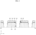
- FIG. 2 illustrates a schematic cross-sectional view illustrating the deposition mask taken along line IIa-IIb of FIG. 1 .
- a deposition mask 100 may include a resin film 110, a non-resin layer 120, and a protective layer 130.
- the resin film 110 may be a film extending on an XY plane, and may form a main body of the deposition mask 100.
- the resin film 110 may include a resin having a low thermal expansion coefficient, e.g., a polyimide (PI) film and the like.
- PI polyimide
- the resin film 110 includes holes 115 penetrating the resin film 110 in a Z direction that is perpendicular to the XY plane.
- the holes 115 may be referred as an opening pattern, and may have a shape corresponding to a pattern of a pattern layer to be deposited using the deposition mask 100.
- the non-resin layer 120 may be positioned or disposed on the resin film 110 overlapping a top surface of the resin film 110.
- the non-resin layer 120 is in contact with the top surface of the resin film 110.
- the non-resin layer 120 may include a conductive material or a magnetic material such that the non-resin layer 120 may be closely or tightly fixed to a substrate to be deposited in a deposition process.
- the non-resin layer 120 may include a magnetic material that may fix the deposition mask 100 to the substrate by positioning a magnet on a first surface of the substrate and a second surface opposite thereto.
- the magnetic material may include iron (Fe), nickel (Ni), cobalt (Co), or an alloy of at least two thereof.
- the non-resin layer 120 may include a conductive material such as a metal that may adsorb and fix the deposition mask 100 to the substrate by positioning an electrostatic chuck at a side of the substrate that faces the deposition mask 100.
- the conductive material may include, titanium (Ti), molybdenum (Mo), ITO, IZO, and the like.
- the non-resin layer 120 may be supported by the resin film 110.
- the non-resin layer 120 may include holes 125 penetrating the non-resin layer 120 in the Z direction.
- the holes 125 may have a shape corresponding to the holes 115 of the resin film 110.
- the holes 125 may include a side surface aligning with an upper side surface of the holes 115 of the resin film 110.
- the holes 115 of the resin film 110 may be tapered as illustrated in FIG. 1 .
- a boundary of the holes 125 of the non-resin layer 120 or a boundary of an uppermost portion of the resin film 110 may be positioned outside a boundary of a lowermost portion of the holes 115 of the resin film 110 on the XY plane.
- the holes 115 and 125 may selectively pass a deposition material through during the deposition process such that the pattern layer that includes a pattern of a predetermined shape may be formed on the substrate.
- the pattern layer may include a light emitting layer for a light emitting diode of a display device.
- the protective layer 130 may be positioned or disposed on the non-resin layer 120.
- the protective layer 130 protects the non-resin layer 120.
- the protective layer 130 may cover and protect a top surface and a side surface of the non-resin layer 120.
- the protective layer 130 may include an upper portion (indicated by 130) positioned or disposed on the top surface of the non-resin layer 120 and overlapping the top surface of the non-resin layer 120, and a lateral portion 136 covering and overlapping the side surface of the non-resin layer 120 that defines the holes 125 of the non-resin layer 120.
- the lateral portion 136 of the protective layer 130 may continuously extend to the upper portion of the protective layer 130.
- the lateral portion 136 of the protective layer 130 may cover a side surface of the resin film 110 that defines the holes 115.
- a lower end of the lateral portion 136 of the protective layer 130 may be positioned lower than the top surface of the non-resin layer 120 such that the lower end of the lateral position 136 may be closer to a bottom surface of the resin film 110.
- the protective layer 130 and the resin film 110 may surround or enclose a portion of the non-resin layer 120 positioned or disposed between adjacent holes 125 such that the portion of the non-resin layer 120 may be sealed off.
- the protective layer 130 may include holes 135 penetrating the protective layer 130 in the Z direction.
- the holes 135 may have a shape corresponding to the holes 115 of the resin film 110.
- the holes 135 may include a side surface that parallels to the side surface of the holes 115 of the resin film 110.
- the holes 135 may be defined by an outer side surface of the lateral portion 136 of the protective layer 130.
- the holes 115 of the resin film 110 may be tapered.
- the holes 135 of the protective layer 130 may be positioned inside the holes 125 of the non-resin layer 120 on the XY plane, and the holes 115 of the resin film 110 may be positioned inside the holes 125 of the non-resin layer 120 on the XY plane.
- the holes 135 of the protective layer 130 may be positioned inside the holes 125 of the non-resin layer 120 on the XY plane, and the holes 115 of the resin film 110 may be positioned inside the holes 135 on the XY plane.
- the protective layer 130 may be in contact with the top surface of the non-resin layer 120, and the lateral portion 136 of the protective layer 130 may be in contact with the side surface of the non-resin layer 120 that defines the holes 125 of the non-resin layer 120.
- the protective layer 130 may be adhered to the non-resin layer 120, and may include a material that is not soluble as a cleaning agent that cleans excess deposition material in the deposition process.
- the protective layer 130 may include a fluorine-based material, e.g., at least one of an organic material containing fluorine, an inorganic material containing fluorine, and a metal material such as molybdenum (Mo) containing fluorine.
- a fluorine-based material e.g., at least one of an organic material containing fluorine, an inorganic material containing fluorine, and a metal material such as molybdenum (Mo) containing fluorine.
- the protective layer 130 including the fluorine-based organic material may be patterned by dissolving only in a fluorine-based organic solvent such as hydrofluoroether (HFE), and the like.
- a fluorine-based organic solvent such as hydrofluoroether (HFE), and the like.
- An organic material containing the fluorine may include about 50 wt% or more.
- the protective layer 130 may not melt when performing deposition on the substrate using the deposition mask 100 according to an embodiment and when cleaning the remaining deposition material. Accordingly, in the cleaning process, the protective layer 130 may protect the non-resin layer 120 such that the non-resin layer 120 may not be exposed to a cleaning solution or ultrasonic waves, thereby damage to the non-resin layer 120 such as peeling may be minimized.
- FIG. 3 illustrates a schematic top plan view of a deposition mask according to an embodiment
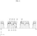
- FIG. 4 illustrates a schematic cross-sectional view illustrating the deposition mask taken along line IVa-IVb of FIG. 3
- the same components as those in FIGS. 1 and 2 are denoted by the same reference numerals, and thus a repeated description thereof will be omitted.
- a deposition mask 100A may be similar to the deposition mask 100 described above, a recess portion (trench) 117 located in the upper portion of the resin film 110 may be included.
- the recess portion 117 may be referred as a hole.
- the recess portion 117 may have various shapes on the XY plane.
- the recess portion 117 may have various polygonal shapes such as a quadrangle , a triangle, a circular shape, an oval shape, but the embodiment is not limited thereto.
- a thickness of the resin film 110 in the recess portion 117 may be greater than zero.
- the non-resin layer 120 may include a hole 127 corresponding to the shape of the recess portion 117 of the resin film 110.
- the hole 127 may penetrate the non-resin layer 120 in the Z direction, and may include a side surface aligning with a side surface of the recess portion 117 of the resin film 110.
- the protective layer 130 may cover the side surface of the resin film 110 that defines the recess portion 117 and the side surface of the non-resin layer 120 that defines the hole 127.
- the protective layer 130 may contact the side surface of the resin film 110 that defines the recess portion 117 and the side surface of the non-resin layer 120 which defines the hole 127.
- a contact area between the protective layer 130 and the resin film 110 may be increased such that contact between the protective layer 130 and the resin film 110 may be improved.
- FIG. 5 illustrates a photograph showing a planar shape of a deposition mask 100c after the deposition process according to a comparative example and a planar shape of a deposition mask 100 after the deposition process according to an embodiment.
- the deposition mask 100c according to the comparative example includes a resin film 110c and a non-resin layer 120c respectively corresponding to the resin film 110 and the non-resin layer 120 of the deposition mask 100 according to the embodiment.
- the resin film 110c has a hole 115c, while the non-resin layer 120c has a hole 125c corresponding to the hole 115c.
- the deposition mask 100c according to the comparative example does not include the protective layer 130 as in the embodiment.
- a portion 129 may peeled off from the non-resin layer 120c by a cleaning solution, ultrasonic waves, or the like, and accordingly, the non-resin layer 120c may be damaged.
- the non-resin layer 120 may be protected by the protective layer 130, and thus damage such as peeling of the non-resin layer 120 may not occur.
- the non-resin layer 120 may be protected by the protective layer 130, and thus damage such as peeling of the non-resin layer 120 may not occur. Accordingly, a protective function of the protective layer 130 with respect to the non-resin layer 120 may be further improved by the recess portion 117 of the resin film 110.
- FIG. 6 illustrates a photograph showing a planar shape of a pattern layer 1000c deposited using the deposition mask 100c according to the comparative example of FIG. 5 and a pattern layer 1000 deposited using the deposition mask according to an embodiment.
- the pattern layer 1000c or 1000 illustrated in FIG. 6 may be an emission layer LEc or LE of an emissive display device, but the disclosure is not limited thereto.
- portion of the non-resin layer 120c may be peeled off during the cleaning process as described above and the deposition mask 100c may be damaged.
- the deposition mask 100c is not closely or tightly fixed to the substrate to be deposited due to the damaged (e.g., de-filmed) non-resin layer 120c. Accordingly, as in the pattern layer 1000c according to the comparative example illustrated in FIG. 6 , precision of the pattern is deteriorated, and a shadow phenomenon occurs.
- the deposition mask 100 since the deposition process is performed using the deposition mask 100 according to the embodiment, damage to the non-resin layer 120 may be prevented, accordingly, the deposition mask 100 may be closely or tightly fixed to the substrate to be deposited by the non-resin layer 120. Accordingly, the precision of the pattern may be maintained as in the pattern layer 1000 according to the embodiment illustrated in FIG. 6 .
- the deposition mask 100A since the deposition process is performed using the deposition mask 100A according to the embodiment of FIG. 3 and FIG. 4 , damage to the non-resin layer 120 may be prevented, accordingly, the deposition mask 100A may be closely or tightly fixed to the substrate to be deposited by the non-resin layer 120. Accordingly, the precision of the pattern may be maintained as in the pattern layer 1000 according to the embodiment illustrated in FIG. 6 .
- a protective function of the protective layer 130 with respect to the non-resin layer 120 may be further improved by the recess portion 117 of the resin film 110 as the pattern layer 1000 according to the embodiment may have a more precise and reliable pattern.
- FIGS. 7 to 12 illustrate schematic cross-sectional views of a manufacturing method of a deposition mask according to an embodiment.
- a resin film 110p is formed by disposing or coating a resin such as polyimide and the like on a carrier substrate 111 such as glass and the like.
- a non-resin layer 120p may be disposed on the resin film 110p by depositing at least one of a magnetic material such as iron (Fe), nickel (Ni), and cobalt (Co), or other suitable materials, or a conductive material such as titanium (Ti), molybdenum (Mo), ITO, and IZO, or other suitable materials.
- a magnetic material such as iron (Fe), nickel (Ni), and cobalt (Co), or other suitable materials
- a conductive material such as titanium (Ti), molybdenum (Mo), ITO, and IZO, or other suitable materials.
- a photoresist pattern 50 may be formed by disposing or stacking a photoresist on the non-resin layer 120p and a photolithography process may be performed.
- the photoresist pattern 50 may include portions 51 and 53 in which a portion of the photoresist may be remained and an opening 55 in which another portion of the photoresist may be removed.
- the photoresist pattern 50 may have a thick portion 51, a thin portion 53 that is thinner than the thick portion 51, and the opening 55 from which the photoresist may be removed.
- the photoresist layer may be exposed by using a photomask including a light-transmitting portion through which light may be transmitted, a light-blocking portion through which light may be blocked, and a halftone portion through which light may be partially transmitted.
- the non-resin layer 120p and the resin film 110p may be etched using the photoresist pattern 50 as a mask to form the holes 115 and 125.
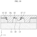
- FIG. 10 illustrate a manufacturing step of the deposition mask according to the embodiment of FIG. 1 and FIG. 2 described above.
- the hole 127 in the non-resin layer 120 and the corresponding recess portion 117 in the resin film 110 may be formed by removing the thin portion 53 of the photoresist pattern 50 and etching the non-resin layer 120p and the resin film 110p that exposed by the remaining photoresist pattern 50.
- the photoresist pattern 50 may be removed.
- a protective layer 130p may be formed by disposing or stacking a fluorine-based material on the non-resin layer 120 by a method such as coating or vacuum deposition.
- a method such as coating or vacuum deposition.
- an example of the protective layer 130p including a photosensitive fluorine-based organic material will be described.
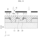
- the protective layer 130p may be exposed through a photomask 60.
- the photomask 60 may include a light-blocking portion 63 and a light-transmitting portion 65 corresponding to the hole 115 of the resin film 110.
- a side surface of the light-transmitting portion 65 of the photomask 60 may be spaced apart from the side surface of the hole 125 of the non-resin layer 120, and may not overlap the bottom surface of the hole 115 of the resin film 110.
- the light-blocking portion 63 of the photomask 60 may overlap the side surface of the hole 125 of the non-resin layer 120, and may not overlap the bottom surface of the hole 115 of the resin film 110.
- FIG. 11 illustrate that the protective layer 130p may include positive photosensitivity.
- the protective layer 130p may include negative photosensitivity
- the light-blocking portion 63 and the light-transmitting portion 65 of the photomask 60 may be variously changed according to the protective layer 130p.
- the exposed protective layer 130p may be developed to complete the protective layer 130 which may include the lateral portion 136 and the hole 135.
- the carrier substrate 111 may be separated from the prepared deposition mask 1000.
- the deposition mask 1000 that separated from the carrier substrate 111 may be attached to a mask frame (not shown) by welding or the like.
- At least some steps of the manufacturing method of the deposition mask described above may not be limited thereto.
- the protective layer 130 when the protective layer 130 may be non-photosensitive, the protective layer 130 according to the embodiment may be formed by etching the protective layer 130p using the photoresist pattern 50 as a mask. For example, by etching the protective layer 130p using the photoresist pattern 50 as a mask after forming the photoresist pattern 50 on the protective layer 130p without direct exposure to the protective layer 130p.
- FIGS. 13 to 16 A description of a deposition mask according to an embodiment follows below with reference to FIGS. 13 to 16 together with FIG. 1 and FIG. 2 described above.
- FIGS. 13 to 16 the same components as those in FIGS. 1 and 2 are denoted by the same reference numerals, and thus a repeated description thereof will be omitted.
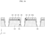
- FIGS. 13 to 16 illustrates a schematic cross-sectional view of a deposition mask according to an embodiment.
- the deposition mask 100 according to the embodiment described above with reference to FIG. 1 , at least one interlayer 140 positioned or disposed on the resin film 110 may be further included.
- the interlayer 140 may be positioned or disposed between the resin film 110 and the non-resin layer 120, and may be formed of (or include) a single layer or multiple layers.
- the interlayer 140 may include an inorganic material such as a silicon oxide (SiO x ) or a silicon nitride (SiN x ), but the disclosure is not limited thereto.
- an inorganic material such as a silicon oxide (SiO x ) or a silicon nitride (SiN x ), but the disclosure is not limited thereto.
- the interlayer 140 may substantially overlap the top surface of the resin film 110, and may have a side surface aligning with the upper side surface of the hole 115 of the resin film 110.
- the interlayer 140 may increase an adhesion between the resin film 110 and the non-resin layer 120.
- an interlayer 140A may be similar to the interlayer 140 described above with reference to FIG. 13 , a lateral portion 146 extending or connecting to the interlayer 140A may be included in addition to the interlayer 140A.
- the lateral portion 146 may cover the side surface of the hole 115 of the resin film 110.
- the deposition mask 100 according to the embodiment described above with reference to FIG. 1 , at least one interlayer 150 positioned or disposed on the non-resin layer 120 may be included.
- the interlayer 150 may be positioned or disposed between the non-resin layer 120 and the protective layer 130, and may be formed of (or include) a single layer or multiple layers.
- the interlayer 150 may include an inorganic material such as a silicon oxide (SiO x ) or a silicon nitride (SiN x ), but the disclosure is not limited thereto.
- an inorganic material such as a silicon oxide (SiO x ) or a silicon nitride (SiN x ), but the disclosure is not limited thereto.
- the interlayer 150 may substantially overlap the top surface of the non-resin 120, and may include a side surface aligning with the upper side surface of the hole 125 of the non-resin 120.
- the interlayer 150 may increase an adhesion between the non-resin 120 and the protective layer 130.
- an interlayer 150A may be similar to the interlayer 150 described above with reference to FIG. 15 , a lateral portion 156 extending or connecting to the interlayer 150A may be included in addition to the interlayer 150A.
- the lateral portion 156 may cover the side surface of the hole 125 of the non-resin layer 120, and may also cover the side surface of the hole 115 of the resin film 110.
- FIGS. 17 to 20 A description of a deposition mask according to an embodiment follows below with reference to FIGS. 17 to 20 together with FIG. 3 and FIG. 4 described above.
- FIGS. 17 to 20 the same components as those in FIG. 3 and FIG. 4 are denoted by the same reference numerals, and thus a repeated description thereof will be omitted.
- FIGS. 17 to 20 illustrates a schematic cross-sectional view of a deposition mask according to an embodiment.
- the deposition mask 100A according to the embodiment as described above with reference to FIG. 3 , at least one interlayer 140B positioned or disposed on the resin film 110 may be further included.
- the interlayer 140B may be positioned or disposed between the resin film 110 and the non-resin layer 120, and may be formed of (or include) a single layer or multiple layers.
- the interlayer 140B may include an inorganic material such as a silicon oxide (SiO x ) or a silicon nitride (SiN x ), but the disclosure is not limited thereto.
- an inorganic material such as a silicon oxide (SiO x ) or a silicon nitride (SiN x ), but the disclosure is not limited thereto.
- the intermediate layer 140B may include a top surface that substantially overlapping the top surface of the resin film 110, a side surface aligning with the upper side surface of the hole 115 of the resin film 110, and another side surface aligning with the side surface of the recess portion 117 of the resin film 110.
- the interlayer 140B may increase an adhesion between the resin film 110 and the non-resin layer 120.
- an interlayer 140C may be similar to the interlayer 140B described above with reference to FIG. 17 , a lateral portion 146C extending or connecting to the interlayer 140C, and portions positioned on the top surface and the side surface of the recess portion 117 of the resin film 110 may be included in addition to the interlayer 140C.
- the interlayer 140C may entirely cover the top and side surfaces of the resin film 110.
- the deposition mask 100A according to the embodiment as described above with reference to FIG. 3 , at least one interlayer 150B positioned or disposed on the non-resin layer 120 may be included.
- the interlayer 150B may be positioned or disposed between the non-resin layer 120 and the protective layer 130, and may be formed of (or include) a single layer or multiple layers.
- the interlayer 150B may include an inorganic material such as a silicon oxide (SiO x ) or a silicon nitride (SiN x ), but the disclosure is not limited thereto.
- an inorganic material such as a silicon oxide (SiO x ) or a silicon nitride (SiN x ), but the disclosure is not limited thereto.
- the interlayer 150B may include a top surface substantially overlapping the top surface of the non-resin 120, a side surface aligning with the upper side surface of the hole 125 of the non-resin 120, and an another side surface aligning with the side surface of the recess portion 117 of the resin film 110.
- the interlayer 150B may increase an adhesion between the non-resin 120 and the protective layer 130.
- an interlayer 150C may be similar to the interlayer 140B as described above with reference to FIG. 19 , a lateral portion 156C extending or extending to the interlayer 150B, and portions positioned or disposed on the top surface and the side surface of the recess portion 117 of the resin film 110 and the side surface of the non-resin layer 120 that aligns with the side surface of the recess portion 117 may be included in addition to the interlayer 150B.
- the lateral portion 156C may cover the side surface of the hole 125 of the non-resin layer 120, and may also cover the side surface of the hole 115 of the resin film 110.
- the interlayer 150B may entirely cover the side surface of the resin film 110, the top surface of the recess portion 117, and the top and side surfaces of the non-resin layer 120.
Landscapes
- Chemical & Material Sciences (AREA)
- Engineering & Computer Science (AREA)
- Chemical Kinetics & Catalysis (AREA)
- Materials Engineering (AREA)
- Mechanical Engineering (AREA)
- Metallurgy (AREA)
- Organic Chemistry (AREA)
- Manufacturing & Machinery (AREA)
- General Chemical & Material Sciences (AREA)
- Physical Vapour Deposition (AREA)
- Electroluminescent Light Sources (AREA)
- Chemical Vapour Deposition (AREA)
Abstract
Description
- The invention relates to a deposition mask.
- The Invention comprises two inventive ideas, the first one being defined in independent claim 1 and the second one independent claim 12, both ideas being closely related to each other.
- An electronic device such as a display device includes a plurality of stacked layers, and at least a layer is formed using a deposition method.
- A pattern layer formed by deposition may be formed by using a deposition mask having an opening pattern formed thereon. The deposition mask includes a fine metal mask made of a metal or an alloy having a low thermal expansion coefficient, such as Invar. Electronic devices such as display devices have recently been becoming larger and higher in resolution, but in the case of the fine metal mask, it is not easy to enlarge an area thereof, and resolution of an opening pattern of the mask is not precise, and thus a deposition mask is desirable including a resin film that is capable of being lighter, being easily thinned, and having a large area as compared with the fine metal mask.
- The above information disclosed in this background section is only for enhancement of understanding of the background of the disclosure, and therefore, it may contain information that does not form the prior art that may already be known to a person of ordinary skill in the art.
- The said problem will be avoided by a deposition mask as per the independent claims.
- The deposition mask capable of minimizing damage such as peeling to a non-resin layer formed on a resin film during a deposition process.
- According to one or more embodiments, a deposition mask includes a resin film including first holes, a non-resin layer disposed on the resin film and including second holes corresponding to the first holes, and a protective layer disposed on the non-resin layer and including third holes corresponding to the first holes, wherein the protective layer includes a first portion disposed on a top surface of the non-resin layer, and a second portion covering a side surface of the second holes of the non-resin layer.
- The protective layer may include at least one of a fluorine-based organic material, a fluorine-based inorganic material, and a fluorine-based metal material.
- The non-resin layer may include at least one of a magnetic material or a conductive material.
- The resin film may include a polyimide (PI).
- The third holes of the protective layer is defined by an outer side surface of the second portion of the protective layer.
- The second portion of the protective layer covers a side surface of the first holes of the resin film.
- The resin film may include a recess portion located in an upper portion of the resin film.
- The non-resin layer may include a fourth hole corresponding to the recess portion.
- The protective layer may cover a side surface of the recess portion and a side surface of the fourth hole of the non-resin layer.
- It may further include an interlayer disposed on the resin film.
- The interlayer may include a portion disposed between the resin film or the non-resin layer and between the non-resin layer and the protective layer.
- The interlayer may include a portion covering a side surface of the first holes of the resin film.
- The interlayer may include an inorganic material.
- According to one or more embodiments, a deposition mask may include a resin film including first holes, a non-resin layer disposed on the resin film and including second holes corresponding to the first holes, and a protective layer disposed on the non-resin layer and including third holes corresponding to the first holes, wherein the protective layer and the resin film surround a portion of the non-resin layer disposed between adjacent second holes such that the portion of the non-resin layer between the adjacent second holes is sealed.
- The protective layer may include at least one of a fluorine-based organic material, a fluorine-based inorganic material, and a fluorine-based metal material.
- The non-resin layer may include at least one of a magnetic material, or a conductive material.
- The resin film may include a recess portion located in an upper portion of the resin film.
- According to one or more embodiments, a deposition mask may include a resin film including first holes, a non-resin layer disposed on the resin film including second holes corresponding to the first holes, and a protective layer disposed on the non-resin layer and including third holes corresponding to the first holes, wherein the resin film includes a recess portion located in an upper portion of the resin film. The protective layer covers a side surface of the recess portion.
- The non-resin layer may include a fourth hole corresponding to the recess portion.
- The protective layer may cover a side surface of the fourth hole of the non-resin layer.
- The non-resin layer may include at least one of a magnetic material and a conductive material.
- According to the embodiments of the disclosure, it may be possible to provide a deposition mask capable of minimizing damage such as peeling to a non-resin layer formed on a resin film during a deposition process.
- The above and other aspects, features, and advantages of embodiments will be more apparent from the following description taken in conjunction with the accompanying drawings, in which:
-
FIG. 1 illustrates a schematic top plan view of a deposition mask according to an embodiment, -
FIG. 2 illustrates a schematic cross-sectional view illustrating the deposition mask taken along line IIa-IIb inFIG. 1 . -
FIG. 3 illustrates a schematic top plan view of a deposition mask according to an embodiment, -
FIG. 4 illustrates a schematic cross-sectional view illustrating the deposition mask taken along line IVa-IVb inFIG. 3 . -
FIG. 5 illustrates a photograph showing a planar shape after a deposition process of a deposition mask according to a comparative example and a deposition mask according to an embodiment. -
FIG. 6 illustrates a photograph showing a planar shape of a pattern layer deposited using a deposition mask according to a comparative example and a pattern layer deposited using a deposition mask according to an embodiment. -
FIGS. 7 to 12 illustrate schematic cross-sectional views of a manufacturing method of a deposition mask according to an embodiment, and -
FIGS. 13 to 20 each illustrate schematic cross-sectional views of a deposition mask according to an embodiment. - Hereinafter, embodiments will be described more fully hereinafter with reference to the accompanying drawings, wherein like reference numerals refer to like elements throughout. As those skilled in the art would realize, the described embodiments may be modified in various different ways, all without departing from the spirit or scope of the disclosure.
- To clearly describes the embodiments, parts that are irrelevant to the description are omitted, and like numerals refer to like or similar constituent elements throughout the specification.
- Reference will now be made in detail to embodiments, examples of which are illustrated in the accompanying drawings, and in the drawings, the same elements are denoted by the same reference numerals, and thus a repeated description thereof will be omitted.
- Further, since sizes and thicknesses of constituent members shown in the accompanying drawings are arbitrarily given for better understanding and ease of description, the embodiments are not limited to the illustrated sizes and thicknesses. In the drawings, the thicknesses of layers, films, panels, regions, etc., are exaggerated for clarity. In the drawings, for better understanding and ease of description, the thicknesses of some layers and areas are exaggerated.
- Accordingly, the embodiments are merely described below, by referring to the figures, to explain aspects of the disclosure. As used herein, the term "and/or" includes any and all combinations of one or more of the associated listed items. Throughout the disclosure, the expression "at least one of a, b, or c" or "at least one of a, b, or c" indicates only a, only b, only c, both a and b, both a and c, both b and c, all of a, b, and c, or variations thereof.
- As the disclosure allows for various changes and numerous embodiments will be illustrated in the drawings and described in the detailed description. Effects and features of the disclosure, and methods for achieving the same will be apparent with reference to embodiments described below in detail with the accompanying drawings. However, the disclosure is not limited to the following embodiments disclosed below and may be implemented in various forms.
- It will be understood that when an element such as a layer, film, region, or substrate is referred to as being "on" another element, it can be directly on the other element or intervening elements may also be present. In contrast, when an element is referred to as being "directly on" another element, there are no intervening elements present. Further, in the specification, the word "on" or "above" means positioned on or below the object portion, and does not necessarily mean positioned on the upper side of the object portion based on a gravitational direction.
- Conversely, when a layer, region, substrate, or area, is referred to as being "directly on" another layer, region, substrate, or area, intervening layers, regions, substrates, or areas, may be absent therebetween. Further when a layer, region, substrate, or area, is referred to as being "below" another layer, region, substrate, or area, it may be directly below the other layer, region, substrate, or area, or intervening layers, regions, substrates, or areas, may be present therebetween. Conversely, when a layer, region, substrate, or area, is referred to as being "directly below" another layer, region, substrate, or area, intervening layers, regions, substrates, or areas, may be absent therebetween.
- In addition, unless explicitly described to the contrary, the word "comprise" and variations such as "comprises" or "comprising" will be understood to imply the inclusion of stated elements but not the exclusion of any other elements.
- In the specification, the phrase "in a plan view" means when an object portion is viewed from above, and the phrase "in a cross-sectional view" means when a cross-section taken by vertically cutting an object portion is viewed from the side.
- Additionally, the terms "overlap" or "overlapped" mean that a first object may be above or below or to a side of a second object, and vice versa. Additionally, the term "overlap" may include layer, stack, face or facing, extending over, covering or partly covering or any other suitable term as would be appreciated and understood by those of ordinary skill in the art. The terms "face" and "facing" mean that a first object may directly or indirectly oppose a second object. In a case in which a third object intervenes between the first and second object, the first and second objects may be understood as being indirectly opposed to one another, although still facing each other.
- The spatially relative terms "below", "beneath", "lower", "above", "upper", or the like, may be used herein for ease of description to describe the relations between one element or component and another element or component as illustrated in the drawings. It will be understood that the spatially relative terms are intended to encompass different orientations of the device in use or operation, in addition to the orientation depicted in the drawings. For example, in the case where a device illustrated in the drawing is turned over, the device positioned "below" or "beneath" another device may be placed "above" another device. Accordingly, the illustrative term "below" may include both the lower and upper positions. The device may also be oriented in other directions and thus the spatially relative terms may be interpreted differently depending on the orientations.
- In addition, in the specification, "connected" means that two or more components are not only directly connected, but two or more components may be connected indirectly through other components, physically connected as well as being electrically connected, or it may be referred to be different names depending on the location or function, but may include connecting each of parts that are substantially integral to each other.
- Although the terms "first," "second," and the like may be used to describe various elements, these elements should not be limited by these terms. These terms are only used to distinguish one element from another.
- As used herein, the singular forms "a," "an," and "the" are intended to include the plural forms as well, unless the context clearly indicates otherwise.
- When an embodiment may be implemented differently, a specific process order may be different from the described order. For example, two consecutively described processes may be performed substantially at the same time or may be performed in an order opposite to the described order.
-
FIG. 1 illustrates a schematic top plan view of a deposition mask according to an embodiment, andFIG. 2 illustrates a schematic cross-sectional view illustrating the deposition mask taken along line IIa-IIb ofFIG. 1 . - A
deposition mask 100 according to an embodiment may include aresin film 110, anon-resin layer 120, and aprotective layer 130. - The
resin film 110 may be a film extending on an XY plane, and may form a main body of thedeposition mask 100. Theresin film 110 may include a resin having a low thermal expansion coefficient, e.g., a polyimide (PI) film and the like. - The
resin film 110 includesholes 115 penetrating theresin film 110 in a Z direction that is perpendicular to the XY plane. Theholes 115 may be referred as an opening pattern, and may have a shape corresponding to a pattern of a pattern layer to be deposited using thedeposition mask 100. - The
non-resin layer 120 may be positioned or disposed on theresin film 110 overlapping a top surface of theresin film 110. - The
non-resin layer 120 is in contact with the top surface of theresin film 110. - The
non-resin layer 120 may include a conductive material or a magnetic material such that thenon-resin layer 120 may be closely or tightly fixed to a substrate to be deposited in a deposition process. - For example, the
non-resin layer 120 may include a magnetic material that may fix thedeposition mask 100 to the substrate by positioning a magnet on a first surface of the substrate and a second surface opposite thereto. The magnetic material may include iron (Fe), nickel (Ni), cobalt (Co), or an alloy of at least two thereof. - For example, the
non-resin layer 120 may include a conductive material such as a metal that may adsorb and fix thedeposition mask 100 to the substrate by positioning an electrostatic chuck at a side of the substrate that faces thedeposition mask 100. The conductive material may include, titanium (Ti), molybdenum (Mo), ITO, IZO, and the like. - The
non-resin layer 120 may be supported by theresin film 110. - The
non-resin layer 120 may includeholes 125 penetrating thenon-resin layer 120 in the Z direction. Theholes 125 may have a shape corresponding to theholes 115 of theresin film 110. Theholes 125 may include a side surface aligning with an upper side surface of theholes 115 of theresin film 110. - The
holes 115 of theresin film 110 may be tapered as illustrated inFIG. 1 . A boundary of theholes 125 of thenon-resin layer 120 or a boundary of an uppermost portion of theresin film 110 may be positioned outside a boundary of a lowermost portion of theholes 115 of theresin film 110 on the XY plane. - The
holes - The
protective layer 130 may be positioned or disposed on thenon-resin layer 120. - The
protective layer 130 protects thenon-resin layer 120. For example, theprotective layer 130 may cover and protect a top surface and a side surface of thenon-resin layer 120. - For example, the
protective layer 130 may include an upper portion (indicated by 130) positioned or disposed on the top surface of thenon-resin layer 120 and overlapping the top surface of thenon-resin layer 120, and alateral portion 136 covering and overlapping the side surface of thenon-resin layer 120 that defines theholes 125 of thenon-resin layer 120. Thelateral portion 136 of theprotective layer 130 may continuously extend to the upper portion of theprotective layer 130. - The
lateral portion 136 of theprotective layer 130 may cover a side surface of theresin film 110 that defines theholes 115. - A lower end of the
lateral portion 136 of theprotective layer 130 may be positioned lower than the top surface of thenon-resin layer 120 such that the lower end of thelateral position 136 may be closer to a bottom surface of theresin film 110. - The
protective layer 130 and theresin film 110 may surround or enclose a portion of thenon-resin layer 120 positioned or disposed betweenadjacent holes 125 such that the portion of thenon-resin layer 120 may be sealed off. - The
protective layer 130 may includeholes 135 penetrating theprotective layer 130 in the Z direction. Theholes 135 may have a shape corresponding to theholes 115 of theresin film 110. Theholes 135 may include a side surface that parallels to the side surface of theholes 115 of theresin film 110. - The
holes 135 may be defined by an outer side surface of thelateral portion 136 of theprotective layer 130. - The
holes 115 of theresin film 110 may be tapered. Theholes 135 of theprotective layer 130 may be positioned inside theholes 125 of thenon-resin layer 120 on the XY plane, and theholes 115 of theresin film 110 may be positioned inside theholes 125 of thenon-resin layer 120 on the XY plane. As another embodiment, theholes 135 of theprotective layer 130 may be positioned inside theholes 125 of thenon-resin layer 120 on the XY plane, and theholes 115 of theresin film 110 may be positioned inside theholes 135 on the XY plane. - The
protective layer 130 may be in contact with the top surface of thenon-resin layer 120, and thelateral portion 136 of theprotective layer 130 may be in contact with the side surface of thenon-resin layer 120 that defines theholes 125 of thenon-resin layer 120. - The
protective layer 130 may be adhered to thenon-resin layer 120, and may include a material that is not soluble as a cleaning agent that cleans excess deposition material in the deposition process. - The
protective layer 130 may include a fluorine-based material, e.g., at least one of an organic material containing fluorine, an inorganic material containing fluorine, and a metal material such as molybdenum (Mo) containing fluorine. - The
protective layer 130 including the fluorine-based organic material may be patterned by dissolving only in a fluorine-based organic solvent such as hydrofluoroether (HFE), and the like. An organic material containing the fluorine may include about 50 wt% or more. - Accordingly, the
protective layer 130 may not melt when performing deposition on the substrate using thedeposition mask 100 according to an embodiment and when cleaning the remaining deposition material. Accordingly, in the cleaning process, theprotective layer 130 may protect thenon-resin layer 120 such that thenon-resin layer 120 may not be exposed to a cleaning solution or ultrasonic waves, thereby damage to thenon-resin layer 120 such as peeling may be minimized. - A description of a deposition mask according to an embodiment follows below with reference to
FIG. 3 andFIG. 4 -
FIG. 3 illustrates a schematic top plan view of a deposition mask according to an embodiment, andFIG. 4 illustrates a schematic cross-sectional view illustrating the deposition mask taken along line IVa-IVb ofFIG. 3 . InFIGS. 3 and4 , the same components as those inFIGS. 1 and2 are denoted by the same reference numerals, and thus a repeated description thereof will be omitted. - A
deposition mask 100A according to an embodiment may be similar to thedeposition mask 100 described above, a recess portion (trench) 117 located in the upper portion of theresin film 110 may be included. Therecess portion 117 may be referred as a hole. - The
recess portion 117 may have various shapes on the XY plane. For example, therecess portion 117 may have various polygonal shapes such as a quadrangle , a triangle, a circular shape, an oval shape, but the embodiment is not limited thereto. - A thickness of the
resin film 110 in therecess portion 117 may be greater than zero. - The
non-resin layer 120 may include ahole 127 corresponding to the shape of therecess portion 117 of theresin film 110. Thehole 127 may penetrate thenon-resin layer 120 in the Z direction, and may include a side surface aligning with a side surface of therecess portion 117 of theresin film 110. - The
protective layer 130 may cover the side surface of theresin film 110 that defines therecess portion 117 and the side surface of thenon-resin layer 120 that defines thehole 127. Theprotective layer 130 may contact the side surface of theresin film 110 that defines therecess portion 117 and the side surface of thenon-resin layer 120 which defines thehole 127. - Accordingly, a contact area between the
protective layer 130 and theresin film 110 may be increased such that contact between theprotective layer 130 and theresin film 110 may be improved. - A description of an effect of the deposition using the
deposition mask 100 according to an embodiment follows below with reference toFIG. 5 andFIG. 6 . -
FIG. 5 illustrates a photograph showing a planar shape of adeposition mask 100c after the deposition process according to a comparative example and a planar shape of adeposition mask 100 after the deposition process according to an embodiment. - Referring to
FIG. 5 , thedeposition mask 100c according to the comparative example includes aresin film 110c and anon-resin layer 120c respectively corresponding to theresin film 110 and thenon-resin layer 120 of thedeposition mask 100 according to the embodiment. Theresin film 110c has ahole 115c, while thenon-resin layer 120c has ahole 125c corresponding to thehole 115c. Thedeposition mask 100c according to the comparative example does not include theprotective layer 130 as in the embodiment. - During a step of cleaning the remaining deposition material in which the deposition process using the
deposition mask 100c according to the comparative example has been performed, aportion 129 may peeled off from thenon-resin layer 120c by a cleaning solution, ultrasonic waves, or the like, and accordingly, thenon-resin layer 120c may be damaged. - However, even after cleaning step in which the deposition process using the
deposition mask 100 according to the embodiment has been performed, thenon-resin layer 120 may be protected by theprotective layer 130, and thus damage such as peeling of thenon-resin layer 120 may not occur. - Also, even when the deposition process is performed using the
deposition mask 100A according to the embodiment illustrated inFIG. 3 andFIG. 4 , thenon-resin layer 120 may be protected by theprotective layer 130, and thus damage such as peeling of thenon-resin layer 120 may not occur. Accordingly, a protective function of theprotective layer 130 with respect to thenon-resin layer 120 may be further improved by therecess portion 117 of theresin film 110. -
FIG. 6 illustrates a photograph showing a planar shape of apattern layer 1000c deposited using thedeposition mask 100c according to the comparative example ofFIG. 5 and apattern layer 1000 deposited using the deposition mask according to an embodiment. - The
pattern layer FIG. 6 may be an emission layer LEc or LE of an emissive display device, but the disclosure is not limited thereto. - When the
deposition mask 100c according to the comparative example is used, portion of thenon-resin layer 120c may be peeled off during the cleaning process as described above and thedeposition mask 100c may be damaged. When an additional deposition process is performed using the damageddeposition mask 100c as described above, thedeposition mask 100c is not closely or tightly fixed to the substrate to be deposited due to the damaged (e.g., de-filmed)non-resin layer 120c. Accordingly, as in thepattern layer 1000c according to the comparative example illustrated inFIG. 6 , precision of the pattern is deteriorated, and a shadow phenomenon occurs. - However, since the deposition process is performed using the
deposition mask 100 according to the embodiment, damage to thenon-resin layer 120 may be prevented, accordingly, thedeposition mask 100 may be closely or tightly fixed to the substrate to be deposited by thenon-resin layer 120. Accordingly, the precision of the pattern may be maintained as in thepattern layer 1000 according to the embodiment illustrated inFIG. 6 . - Also, since the deposition process is performed using the
deposition mask 100A according to the embodiment ofFIG. 3 andFIG. 4 , damage to thenon-resin layer 120 may be prevented, accordingly, thedeposition mask 100A may be closely or tightly fixed to the substrate to be deposited by thenon-resin layer 120. Accordingly, the precision of the pattern may be maintained as in thepattern layer 1000 according to the embodiment illustrated inFIG. 6 . A protective function of theprotective layer 130 with respect to thenon-resin layer 120 may be further improved by therecess portion 117 of theresin film 110 as thepattern layer 1000 according to the embodiment may have a more precise and reliable pattern. - A description of a manufacturing method of a deposition mask according to an embodiment follows below with reference to
FIGS. 7 to 12 together with the previously described drawings. -
FIGS. 7 to 12 illustrate schematic cross-sectional views of a manufacturing method of a deposition mask according to an embodiment. - Referring to
FIG. 7 , aresin film 110p is formed by disposing or coating a resin such as polyimide and the like on acarrier substrate 111 such as glass and the like. - A
non-resin layer 120p may be disposed on theresin film 110p by depositing at least one of a magnetic material such as iron (Fe), nickel (Ni), and cobalt (Co), or other suitable materials, or a conductive material such as titanium (Ti), molybdenum (Mo), ITO, and IZO, or other suitable materials. - Referring to
FIG. 8 , aphotoresist pattern 50 may be formed by disposing or stacking a photoresist on thenon-resin layer 120p and a photolithography process may be performed. - In the embodiment illustrated in
FIG. 1 andFIG. 2 described above, thephotoresist pattern 50 may includeportions opening 55 in which another portion of the photoresist may be removed. - However, in the embodiment illustrated in
FIG. 3 andFIG. 4 described above, thephotoresist pattern 50 may have athick portion 51, athin portion 53 that is thinner than thethick portion 51, and theopening 55 from which the photoresist may be removed. The photoresist layer may be exposed by using a photomask including a light-transmitting portion through which light may be transmitted, a light-blocking portion through which light may be blocked, and a halftone portion through which light may be partially transmitted. - Referring to
FIG. 9 , thenon-resin layer 120p and theresin film 110p may be etched using thephotoresist pattern 50 as a mask to form theholes -
FIG. 10 illustrate a manufacturing step of the deposition mask according to the embodiment ofFIG. 1 andFIG. 2 described above. However, in the embodiment illustrated inFIGS. 3 and4 described above, thehole 127 in thenon-resin layer 120 and thecorresponding recess portion 117 in theresin film 110 may be formed by removing thethin portion 53 of thephotoresist pattern 50 and etching thenon-resin layer 120p and theresin film 110p that exposed by the remainingphotoresist pattern 50. - Then, the
photoresist pattern 50 may be removed. - Referring to
FIG. 10 , aprotective layer 130p may be formed by disposing or stacking a fluorine-based material on thenon-resin layer 120 by a method such as coating or vacuum deposition. In the embodiment, an example of theprotective layer 130p including a photosensitive fluorine-based organic material will be described. - Referring to
FIG. 11 , theprotective layer 130p may be exposed through aphotomask 60. When theprotective layer 130p including positive photosensitivity, thephotomask 60 may include a light-blockingportion 63 and a light-transmittingportion 65 corresponding to thehole 115 of theresin film 110. - In the embodiment, on the XY plane, a side surface of the light-transmitting
portion 65 of thephotomask 60 may be spaced apart from the side surface of thehole 125 of thenon-resin layer 120, and may not overlap the bottom surface of thehole 115 of theresin film 110. For example, the light-blockingportion 63 of thephotomask 60 may overlap the side surface of thehole 125 of thenon-resin layer 120, and may not overlap the bottom surface of thehole 115 of theresin film 110. -
FIG. 11 illustrate that theprotective layer 130p may include positive photosensitivity. However, in another embodiment, theprotective layer 130p may include negative photosensitivity, the light-blockingportion 63 and the light-transmittingportion 65 of thephotomask 60 may be variously changed according to theprotective layer 130p. - Referring to
FIG. 12 , the exposedprotective layer 130p may be developed to complete theprotective layer 130 which may include thelateral portion 136 and thehole 135. - After the
protective layer 130 including thelateral portion 136 and thehole 136 may be formed, thecarrier substrate 111 may be separated from theprepared deposition mask 1000. - The
deposition mask 1000 that separated from thecarrier substrate 111 may be attached to a mask frame (not shown) by welding or the like. - At least some steps of the manufacturing method of the deposition mask described above may not be limited thereto.
- For example, when the
protective layer 130 may be non-photosensitive, theprotective layer 130 according to the embodiment may be formed by etching theprotective layer 130p using thephotoresist pattern 50 as a mask. For example, by etching theprotective layer 130p using thephotoresist pattern 50 as a mask after forming thephotoresist pattern 50 on theprotective layer 130p without direct exposure to theprotective layer 130p. - A description of a deposition mask according to an embodiment follows below with reference to
FIGS. 13 to 16 together withFIG. 1 andFIG. 2 described above. InFIGS. 13 to 16 , the same components as those inFIGS. 1 and2 are denoted by the same reference numerals, and thus a repeated description thereof will be omitted. - Each of
FIGS. 13 to 16 illustrates a schematic cross-sectional view of a deposition mask according to an embodiment. - Referring to
FIG. 13 , thedeposition mask 100 according to the embodiment described above with reference toFIG. 1 , at least oneinterlayer 140 positioned or disposed on theresin film 110 may be further included. - The
interlayer 140 may be positioned or disposed between theresin film 110 and thenon-resin layer 120, and may be formed of (or include) a single layer or multiple layers. - The
interlayer 140 may include an inorganic material such as a silicon oxide (SiOx) or a silicon nitride (SiNx), but the disclosure is not limited thereto. - The
interlayer 140 may substantially overlap the top surface of theresin film 110, and may have a side surface aligning with the upper side surface of thehole 115 of theresin film 110. - The
interlayer 140 may increase an adhesion between theresin film 110 and thenon-resin layer 120. - Referring to
FIG. 14 , aninterlayer 140A according to an embodiment may be similar to theinterlayer 140 described above with reference toFIG. 13 , alateral portion 146 extending or connecting to theinterlayer 140A may be included in addition to theinterlayer 140A. - The
lateral portion 146 may cover the side surface of thehole 115 of theresin film 110. - Referring to
FIG. 15 , thedeposition mask 100 according to the embodiment described above with reference toFIG. 1 , at least oneinterlayer 150 positioned or disposed on thenon-resin layer 120 may be included. - The
interlayer 150 may be positioned or disposed between thenon-resin layer 120 and theprotective layer 130, and may be formed of (or include) a single layer or multiple layers. - The
interlayer 150 may include an inorganic material such as a silicon oxide (SiOx) or a silicon nitride (SiNx), but the disclosure is not limited thereto. - The
interlayer 150 may substantially overlap the top surface of the non-resin 120, and may include a side surface aligning with the upper side surface of thehole 125 of the non-resin 120. - The
interlayer 150 may increase an adhesion between the non-resin 120 and theprotective layer 130. - Referring to
FIG. 16 , aninterlayer 150A according to the an embodiment may be similar to theinterlayer 150 described above with reference toFIG. 15 , alateral portion 156 extending or connecting to theinterlayer 150A may be included in addition to theinterlayer 150A. - The
lateral portion 156 may cover the side surface of thehole 125 of thenon-resin layer 120, and may also cover the side surface of thehole 115 of theresin film 110. - A description of a deposition mask according to an embodiment follows below with reference to
FIGS. 17 to 20 together withFIG. 3 andFIG. 4 described above. InFIGS. 17 to 20 , the same components as those inFIG. 3 andFIG. 4 are denoted by the same reference numerals, and thus a repeated description thereof will be omitted. - Each of
FIGS. 17 to 20 illustrates a schematic cross-sectional view of a deposition mask according to an embodiment. - Referring to
FIG. 17 , thedeposition mask 100A according to the embodiment as described above with reference toFIG. 3 , at least oneinterlayer 140B positioned or disposed on theresin film 110 may be further included. - The
interlayer 140B may be positioned or disposed between theresin film 110 and thenon-resin layer 120, and may be formed of (or include) a single layer or multiple layers. - The
interlayer 140B may include an inorganic material such as a silicon oxide (SiOx) or a silicon nitride (SiNx), but the disclosure is not limited thereto. - The
intermediate layer 140B may include a top surface that substantially overlapping the top surface of theresin film 110, a side surface aligning with the upper side surface of thehole 115 of theresin film 110, and another side surface aligning with the side surface of therecess portion 117 of theresin film 110. - The
interlayer 140B may increase an adhesion between theresin film 110 and thenon-resin layer 120. - Referring to
FIG. 18 , aninterlayer 140C according to an embodiment may be similar to theinterlayer 140B described above with reference toFIG. 17 , alateral portion 146C extending or connecting to theinterlayer 140C, and portions positioned on the top surface and the side surface of therecess portion 117 of theresin film 110 may be included in addition to theinterlayer 140C. - The
interlayer 140C may entirely cover the top and side surfaces of theresin film 110. - Referring to
FIG. 19 , thedeposition mask 100A according to the embodiment as described above with reference toFIG. 3 , at least oneinterlayer 150B positioned or disposed on thenon-resin layer 120 may be included. - The
interlayer 150B may be positioned or disposed between thenon-resin layer 120 and theprotective layer 130, and may be formed of (or include) a single layer or multiple layers. - The
interlayer 150B may include an inorganic material such as a silicon oxide (SiOx) or a silicon nitride (SiNx), but the disclosure is not limited thereto. - The
interlayer 150B may include a top surface substantially overlapping the top surface of the non-resin 120, a side surface aligning with the upper side surface of thehole 125 of the non-resin 120, and an another side surface aligning with the side surface of therecess portion 117 of theresin film 110. - The
interlayer 150B may increase an adhesion between the non-resin 120 and theprotective layer 130. - Referring to
FIG. 20 , aninterlayer 150C according to an embodiment may be similar to theinterlayer 140B as described above with reference toFIG. 19 , alateral portion 156C extending or extending to theinterlayer 150B, and portions positioned or disposed on the top surface and the side surface of therecess portion 117 of theresin film 110 and the side surface of thenon-resin layer 120 that aligns with the side surface of therecess portion 117 may be included in addition to theinterlayer 150B. - The
lateral portion 156C may cover the side surface of thehole 125 of thenon-resin layer 120, and may also cover the side surface of thehole 115 of theresin film 110. - The
interlayer 150B may entirely cover the side surface of theresin film 110, the top surface of therecess portion 117, and the top and side surfaces of thenon-resin layer 120.
Claims (17)
- A deposition mask (100) comprising:a resin film (110) including first holes;a non-resin layer (120) disposed on the resin film (110) and including second holes corresponding to the first holes;characterized bya protective layer (130) disposed on the non-resin layer (120) and including third holes corresponding to the first holes, whereinthe protective layer (130) includes:a first portion disposed on a top surface of the non-resin layer (120); anda second portion covering a side surface of the second holes of the non-resin layer (120).
- The deposition mask (100) of claim 1, wherein the resin film (110) includes a polyimide (PI).
- The deposition mask (100) of at least one of claims 1 or 2, wherein the third holes of the protective layer (130) are defined by an outer side surface of the second portion of the protective layer (130).
- The deposition mask (100) of at least one of claims 1 to 3, wherein the second portion of the protective layer (130) covers a side surface of the first holes of the resin film (110).
- The deposition mask (100) of at least one of claims 1 to 4 , wherein the protective layer (130) covers a side surface of the recess portion (117) and a side surface of the fourth hole of the non-resin layer (120).
- The deposition mask (100) of at least one of claims 1 to 5, further comprising:
an interlayer (140, 150) disposed on the resin film (110). - The deposition mask (100) of claim 6, wherein the interlayer (140, 150) includes a portion disposed between the resin film (110) and the non-resin layer (120) or between the non-resin layer (120) and the protective layer (130).
- The deposition mask (100) of at least one of claims 6 or 7, wherein the interlayer (140, 150) includes a portion covering a side surface of the first holes of the resin film (110).
- The deposition mask (100) of at least one of claims 6 top 9, wherein the interlayer (140, 150) includes a portion disposed between the resin film (110) and the non-resin layer (120) or between the non-resin layer (120) and the protective layer (130).
- The deposition mask (100) of at least one of claims 6 to 9, wherein the interlayer (140, 150) includes a portion covering a side surface of the first holes of the resin film (110).
- The deposition mask (100) of at least one of claims 6 to 10, wherein the interlayer (140, 150) includes an inorganic material.
- A deposition mask (100) comprising:a resin film (110) including first holes;a non-resin layer (120) disposed on the resin film (110) and including second holes corresponding to the first holes; anda protective layer (130) disposed on the non-resin layer (120) and including third holes corresponding to the first holes, whereinthe protective layer (130) and the resin film (110) surround a portion of the non-resin layer (120) disposed between adjacent second holes such that the portion of the non-resin layer (120) between the adjacent second holes is sealed.
- The deposition mask (100) of at least one of claims 1 to 12, wherein the protective layer (130) includes at least one of a fluorine-based organic material, a fluorine-based inorganic material, and a fluorine-based metal material.
- The deposition mask (100) of at least one of claims 1 to 13, wherein the resin film (110) includes a recess portion (117) located in an upper portion of the resin film (110).
- A deposition mask (100) comprising:a resin film (110) including first holes;characterized bya non-resin layer (120) disposed on the resin film (110) and including second holes corresponding to the first holes; anda protective layer (130) disposed on the non-resin layer (120) and including third holes corresponding to the first holes, whereinthe resin film (110) includes a recess portion (117) located in an upper portion of the resin film (110).
- The deposition mask (100) of at least one of claims 1 to 15, wherein the non-resin layer (120) includes a fourth hole corresponding to the recess portion (117).
- The deposition mask (100) of at least one of claims 1 to 16, wherein the protective layer (130) covers a side surface of the fourth hole of the non-resin layer (120).
Applications Claiming Priority (1)
| Application Number | Priority Date | Filing Date | Title |
|---|---|---|---|
| KR1020210101215A KR20230020035A (en) | 2021-08-02 | 2021-08-02 | Mask for Deposition |
Publications (2)
| Publication Number | Publication Date |
|---|---|
| EP4130330A2 true EP4130330A2 (en) | 2023-02-08 |
| EP4130330A3 EP4130330A3 (en) | 2023-06-07 |
Family
ID=82786283
Family Applications (1)
| Application Number | Title | Priority Date | Filing Date |
|---|---|---|---|
| EP22188076.8A Pending EP4130330A3 (en) | 2021-08-02 | 2022-08-01 | Mask for deposition |
Country Status (4)
| Country | Link |
|---|---|
| US (2) | US12103024B2 (en) |
| EP (1) | EP4130330A3 (en) |
| KR (1) | KR20230020035A (en) |
| CN (1) | CN115701455A (en) |
Families Citing this family (1)
| Publication number | Priority date | Publication date | Assignee | Title |
|---|---|---|---|---|
| CN210916231U (en) * | 2019-10-18 | 2020-07-03 | 昆山国显光电有限公司 | Mask plate |
Family Cites Families (99)
| Publication number | Priority date | Publication date | Assignee | Title |
|---|---|---|---|---|
| JPS6142388U (en) | 1984-08-23 | 1986-03-18 | トヨタ自動車株式会社 | Vehicle front lift reduction device |
| KR19990011944A (en) * | 1997-07-25 | 1999-02-18 | 손욱 | LCD |
| JP4218896B2 (en) * | 2005-03-02 | 2009-02-04 | Tdk株式会社 | Magnetic recording medium, recording / reproducing apparatus, and stamper |
| JP3918003B2 (en) * | 2005-03-10 | 2007-05-23 | Tdk株式会社 | Magnetic recording medium, recording / reproducing apparatus, and stamper |
| JP4058444B2 (en) * | 2005-11-15 | 2008-03-12 | Tdk株式会社 | Stamper, imprint method, and information recording medium manufacturing method |
| CN101416294B (en) * | 2006-03-30 | 2011-03-30 | 株式会社美高仁工业 | Method of forming micro metal bump |
| DE102006022722B4 (en) * | 2006-05-12 | 2010-06-17 | Hueck Engraving Gmbh & Co. Kg | Method and device for surface structuring of a press plate or an endless belt |
| DE112006003899T5 (en) * | 2006-05-17 | 2009-04-30 | Shinko Electric Industries Co., Ltd. | Process for forming a resist pattern, process for producing a printed circuit board and printed circuit board |
| KR101381252B1 (en) * | 2007-06-05 | 2014-04-04 | 삼성디스플레이 주식회사 | Imprint device, method of fabricating the same, method of patterning thin film using the same |
| JP2009154407A (en) * | 2007-12-27 | 2009-07-16 | Tdk Corp | Peeling device, peeling method, and information recording medium manufacturing method |
| KR20090130760A (en) * | 2008-06-16 | 2009-12-24 | 삼성전자주식회사 | A liquid crystal display device having a viewing angle controlled by using a stripe diffuser, a manufacturing method thereof, and a stripe diffuser |
| JP5295751B2 (en) * | 2008-12-25 | 2013-09-18 | 大日本スクリーン製造株式会社 | Zinc oxide film forming method and zinc oxide film forming apparatus |
| US8349143B2 (en) * | 2008-12-30 | 2013-01-08 | Intermolecular, Inc. | Shadow masks for patterned deposition on substrates |
| KR101073544B1 (en) * | 2009-08-21 | 2011-10-14 | 삼성모바일디스플레이주식회사 | Mask and method for fabricating thereof |
| JP2011181123A (en) * | 2010-02-26 | 2011-09-15 | Fuji Electric Device Technology Co Ltd | Method of manufacturing magnetic recording medium |
| JP2013021165A (en) * | 2011-07-12 | 2013-01-31 | Sony Corp | Mask for vapor deposition, manufacturing method of mask for vapor deposition, electronic element, and manufacturing method of electronic element |
| KR101860493B1 (en) * | 2011-10-20 | 2018-05-24 | 삼성디스플레이 주식회사 | Method of forming fine pattern mask and method of forming fine pattenr using the same |
| JP5288074B2 (en) * | 2012-01-12 | 2013-09-11 | 大日本印刷株式会社 | Method for manufacturing multi-sided deposition mask, multi-sided deposition mask obtained thereby, and method for producing organic semiconductor element |
| CN105779934B (en) * | 2012-01-12 | 2020-05-22 | 大日本印刷株式会社 | Manufacturing method of vapor deposition mask and manufacturing method of organic semiconductor element |
| TWI687315B (en) * | 2012-01-12 | 2020-03-11 | 日商大日本印刷股份有限公司 | Vapor deposition mask, pattern manufacturing method, organic semiconductor element manufacturing method |
| CN114089600B (en) * | 2012-03-15 | 2024-12-03 | 富士胶片株式会社 | Electrostatic capacitance input device and manufacturing method thereof, and image display device |
| KR20130114998A (en) * | 2012-04-10 | 2013-10-21 | 삼성디스플레이 주식회사 | Liquid crystal display device and method for manufacturing the same |
| JP6142194B2 (en) * | 2012-11-15 | 2017-06-07 | 株式会社ブイ・テクノロジー | Vapor deposition mask manufacturing method and vapor deposition mask |
| KR101978190B1 (en) * | 2012-11-29 | 2019-05-15 | 삼성디스플레이 주식회사 | Polarizer and method of manufacturing the same |
| US9704824B2 (en) * | 2013-01-03 | 2017-07-11 | STATS ChipPAC Pte. Ltd. | Semiconductor device and method of forming embedded wafer level chip scale packages |
| KR101934244B1 (en) * | 2013-03-26 | 2018-12-31 | 다이니폰 인사츠 가부시키가이샤 | Deposition mask, preparatory body for deposition mask, method for manufacturing deposition mask, and method for manufacturing organic semiconductor element |
| JP6142388B2 (en) | 2013-04-09 | 2017-06-07 | 株式会社ブイ・テクノロジー | Vapor deposition mask and vapor deposition mask manufacturing method |
| TWI737969B (en) * | 2013-04-12 | 2021-09-01 | 日商大日本印刷股份有限公司 | Vapor deposition mask for the manufacture of organic semiconductor elements, manufacturing method of vapor deposition mask for the manufacture of organic semiconductor elements, vapor deposition mask preparations for the manufacture of organic semiconductor elements, pattern formation method, and organic semiconductor elements Manufacturing method |
| JP6331276B2 (en) * | 2013-06-28 | 2018-05-30 | セイコーエプソン株式会社 | Electro-optical device, method of manufacturing electro-optical device, and electronic apparatus |
| KR102204976B1 (en) * | 2013-11-13 | 2021-01-20 | 삼성디스플레이 주식회사 | Display apparatus and fabrication method thereof |
| JP6288497B2 (en) * | 2013-12-13 | 2018-03-07 | 株式会社ブイ・テクノロジー | Mask and manufacturing method thereof |
| JP6357777B2 (en) | 2014-01-08 | 2018-07-18 | 大日本印刷株式会社 | Method for manufacturing laminated mask |
| JP2015148002A (en) * | 2014-02-07 | 2015-08-20 | 大日本印刷株式会社 | Vapor deposition mask, vapor deposition mask preparation, and method for manufacturing organic semiconductor element |
| KR20150095971A (en) * | 2014-02-12 | 2015-08-24 | 삼성디스플레이 주식회사 | Master mold, imprint mold and method of manufacturing display device using the imprint mold |
| US10573815B2 (en) * | 2014-06-06 | 2020-02-25 | Dai Nippon Printing Co., Ltd. | Vapor deposition mask, frame-equipped vapor deposition mask, vapor deposition mask preparation body, and method for producing organic semiconductor element |
| WO2016060216A1 (en) * | 2014-10-15 | 2016-04-21 | シャープ株式会社 | Deposition mask, deposition device, deposition method, and deposition mask manufacturing method |
| KR102303994B1 (en) * | 2014-10-20 | 2021-09-23 | 삼성디스플레이 주식회사 | Method for manufacturing substrate for organic light emitting diode |
| CN107075658B (en) * | 2014-10-23 | 2019-02-19 | 夏普株式会社 | Manufacturing method of vapor deposition mask, vapor deposition mask, vapor deposition apparatus, vapor deposition method |
| KR102226601B1 (en) * | 2014-12-02 | 2021-03-15 | 삼성디스플레이 주식회사 | Touch panel and method of manufacturing the same |
| US20170362698A1 (en) * | 2014-12-03 | 2017-12-21 | Sharp Kabushiki Kaisha | Vapor deposition mask, vapor deposition device, method for manufacturing vapor deposition mask, and vapor deposition method |
| KR20160069048A (en) * | 2014-12-05 | 2016-06-16 | 삼성디스플레이 주식회사 | Wire grid polarizer and method for fabricating the same |
| US10384417B2 (en) * | 2015-01-20 | 2019-08-20 | Sharp Kabushiki Kaisha | Deposition mask and manufacturing method |
| KR102329870B1 (en) * | 2015-02-13 | 2021-11-24 | 삼성디스플레이 주식회사 | Thin film transistor array substrate and manufacturing method of the same |
| KR20160119896A (en) * | 2015-04-06 | 2016-10-17 | 삼성디스플레이 주식회사 | Imprint lithography method, method for manufacturing master template using the method and master template manufactured by the method |
| KR102306655B1 (en) * | 2015-04-10 | 2021-09-29 | 삼성디스플레이 주식회사 | Liquid crystal display and method for manufacturing the same |
| US9989845B2 (en) * | 2015-04-16 | 2018-06-05 | Samsung Display Co., Ltd. | Imprint lithography method, method for manufacturing master template using the method and master template manufactured by the method |
| JP6160747B2 (en) * | 2015-07-03 | 2017-07-12 | 大日本印刷株式会社 | Vapor deposition mask manufacturing method, vapor deposition mask preparation, organic semiconductor element manufacturing method, and vapor deposition mask |
| KR102071840B1 (en) * | 2015-07-17 | 2020-01-31 | 도판 인사츠 가부시키가이샤 | Metal mask base material, metal mask, and manufacturing method of metal mask |
| JP6466589B2 (en) * | 2015-09-30 | 2019-02-06 | 鴻海精密工業股▲ふん▼有限公司Hon Hai Precision Industry Co.,Ltd. | Manufacturing method of resin film having fine pattern, manufacturing method of organic EL display device, substrate film for forming fine pattern and resin film with support member |
| WO2017069066A1 (en) * | 2015-10-21 | 2017-04-27 | シャープ株式会社 | Metal mask for scan deposition, deposition device, deposition method, and electroluminescent display device |
| JP6417486B2 (en) | 2015-12-25 | 2018-11-07 | 鴻海精密工業股▲ふん▼有限公司 | Vapor deposition mask and organic semiconductor device manufacturing method |
| WO2017130440A1 (en) * | 2016-01-26 | 2017-08-03 | 鴻海精密工業股▲ふん▼有限公司 | Vapor deposition mask, manufacturing method thereof, and manufacturing method for organic light-emitting diode using vapor deposition mask |
| JP6690814B2 (en) | 2016-01-27 | 2020-04-28 | エルジー・ケム・リミテッド | Film mask, method for manufacturing the same, and pattern forming method using the same |
| US11233199B2 (en) * | 2016-02-10 | 2022-01-25 | Hon Hai Precision Industry Co., Ltd. | Vapor deposition mask manufacturing method, vapor deposition mask, and organic semiconductor element manufacturing method |
| WO2017145402A1 (en) * | 2016-02-23 | 2017-08-31 | 鴻海精密工業股▲ふん▼有限公司 | Vapor deposition mask, vapor deposition mask manufacturing method, and organic el display device manufacturing method |
| JP6681739B2 (en) | 2016-02-25 | 2020-04-15 | 株式会社ジャパンディスプレイ | Method for manufacturing shadow mask and method for manufacturing display device |
| JP6407479B2 (en) * | 2016-03-23 | 2018-10-17 | 鴻海精密工業股▲ふん▼有限公司 | Vapor deposition apparatus, vapor deposition method, and organic EL display device manufacturing method |
| US10934614B2 (en) * | 2016-03-23 | 2021-03-02 | Hon Hai Precision Industry Co., Ltd. | Vapor deposition mask, vapor deposition mask production method, and organic semiconductor element production method |
| KR102526936B1 (en) * | 2016-04-26 | 2023-04-28 | 삼성디스플레이 주식회사 | Display panel and mother substrate for display panel |
| CN205576262U (en) * | 2016-05-09 | 2016-09-14 | 鄂尔多斯市源盛光电有限责任公司 | Mask plate |
| US9748156B1 (en) * | 2016-06-13 | 2017-08-29 | Taiwan Semiconductor Manufacturing Co., Ltd. | Semiconductor package assembly, semiconductor package and forming method thereof |
| KR20180009825A (en) * | 2016-07-19 | 2018-01-30 | 삼성디스플레이 주식회사 | Roll type imprint master mold, manufacturing the same, and imprint method using the same |
| JP6949507B2 (en) | 2016-08-05 | 2021-10-13 | 日鉄ケミカル&マテリアル株式会社 | Thin-film mask and its manufacturing method, and laminated body for thin-film mask and its manufacturing method |
| KR20180023102A (en) * | 2016-08-23 | 2018-03-07 | 삼성디스플레이 주식회사 | Wire grid pattern and method for fabricating the same |
| KR102697540B1 (en) * | 2016-09-27 | 2024-08-23 | 삼성디스플레이 주식회사 | Method of manufacturing imprint master template |
| CN113463017A (en) * | 2016-09-30 | 2021-10-01 | 大日本印刷株式会社 | Frame-integrated vapor deposition mask, production body and production method therefor, and vapor deposition pattern formation method |
| KR102444139B1 (en) * | 2016-10-06 | 2022-09-15 | 다이니폰 인사츠 가부시키가이샤 | A method for manufacturing a deposition mask, a method for manufacturing an organic semiconductor element, and a method for manufacturing an organic EL display |
| KR20180039228A (en) * | 2016-10-07 | 2018-04-18 | 삼성디스플레이 주식회사 | Method of manufacturing display apparatus |
| WO2018092182A1 (en) * | 2016-11-15 | 2018-05-24 | シャープ株式会社 | Vapor deposition mask, vapor deposition apparatus, vapor deposition mask production method, and electroluminescent display apparatus production method |
| KR102609073B1 (en) * | 2016-11-30 | 2023-12-05 | 엘지디스플레이 주식회사 | Mask for deposition, manufacturing method of the same |
| US20190345596A1 (en) * | 2016-12-02 | 2019-11-14 | Sharp Kabushiki Kaisha | Vapor deposition mask, vapor deposition device, method of manufacturing vapor deposition mask, and method of manufacturing electroluminescence display device |
| CN110214198A (en) * | 2017-01-26 | 2019-09-06 | 夏普株式会社 | Mask for vapor deposition, manufacturing method of mask for vapor deposition, and manufacturing method of organic EL display device |
| JP6620899B2 (en) * | 2017-03-31 | 2019-12-18 | 大日本印刷株式会社 | Vapor deposition mask, vapor deposition mask with frame, vapor deposition mask preparation, vapor deposition pattern forming method, and organic semiconductor element manufacturing method |
| KR102404724B1 (en) * | 2017-06-07 | 2022-06-02 | 삼성디스플레이 주식회사 | Display device |
| KR102300028B1 (en) * | 2017-06-08 | 2021-09-09 | 삼성디스플레이 주식회사 | Manufacturing method of organic light emitting display device |
| TWI649787B (en) * | 2017-07-12 | 2019-02-01 | 林義溢 | Multi-layer mask |
| US10439138B2 (en) * | 2017-08-31 | 2019-10-08 | Sakai Display Products Corporation | Method for producing deposition mask |
| WO2019064473A1 (en) * | 2017-09-29 | 2019-04-04 | シャープ株式会社 | Vapor deposition mask, manufacturing method for vapor deposition mask, and manufacturing method for display device |
| KR102690889B1 (en) * | 2018-06-07 | 2024-08-01 | 삼성디스플레이 주식회사 | Display device and manufacturing method thereof |
| KR102632165B1 (en) * | 2018-07-10 | 2024-02-01 | 삼성디스플레이 주식회사 | Display device and manufacturing method thereof |
| US20210265602A1 (en) * | 2018-08-08 | 2021-08-26 | Sakai Display Products Corporation | Vapor deposition mask, method for manufacturing vapor deposition mask, and method for manufacturing organic semiconductor element |
| KR102618040B1 (en) * | 2018-08-09 | 2023-12-27 | 삼성디스플레이 주식회사 | Method for manufacturing display apparatus and display apparatus manufactured thereby |
| KR102666843B1 (en) * | 2018-08-31 | 2024-05-21 | 삼성디스플레이 주식회사 | Master stamp for nano imprint and method of manufacturing of the smae |
| KR102537379B1 (en) * | 2018-12-21 | 2023-05-26 | 삼성디스플레이 주식회사 | Light emitting diode display device |
| KR102543443B1 (en) * | 2019-03-08 | 2023-06-14 | 삼성디스플레이 주식회사 | Display device and method of manufacturing the flexible printed circuit board |
| CN113646461A (en) * | 2019-04-01 | 2021-11-12 | 堺显示器制品株式会社 | Manufacturing method of film-forming mask |
| KR102207286B1 (en) | 2019-07-19 | 2021-01-25 | 인하대학교 산학협력단 | Highly fluorinated polymer photoresist containing a spiropyran unit and method for manufacturing organic electronic device using the same |
| CN113099731B (en) * | 2019-10-23 | 2024-10-22 | 京东方科技集团股份有限公司 | Display substrate and manufacturing method thereof, and display device |
| CN118488767A (en) * | 2019-10-29 | 2024-08-13 | 京东方科技集团股份有限公司 | Display substrate and display device |
| KR20210078620A (en) * | 2019-12-18 | 2021-06-29 | 삼성디스플레이 주식회사 | Display device |
| JP7612327B2 (en) * | 2019-12-24 | 2025-01-14 | 日東電工株式会社 | Method for manufacturing a wired circuit board and wired circuit board sheet |
| KR20210091383A (en) * | 2020-01-13 | 2021-07-22 | 삼성디스플레이 주식회사 | Mask, method of manufacturing the same, and method of manufacturing display panel |
| KR20210091382A (en) | 2020-01-13 | 2021-07-22 | 삼성디스플레이 주식회사 | Mask, method of manufacturing the same, and method of manufacturing display panel |
| US11638388B2 (en) * | 2020-05-15 | 2023-04-25 | The Hong Kong University Of Science And Technology | High-resolution shadow masks |
| CN114005848B (en) * | 2020-07-28 | 2024-09-03 | 合肥鑫晟光电科技有限公司 | A driving backplane, a manufacturing method thereof, a backlight module and a display device |
| KR20220021994A (en) * | 2020-08-14 | 2022-02-23 | 삼성디스플레이 주식회사 | Mask, method of manufacturing the same, and method of manufacturing display panel |
| KR20220149853A (en) * | 2021-04-30 | 2022-11-09 | 삼성디스플레이 주식회사 | Display device and method for fabricating the same |
| KR102925520B1 (en) * | 2021-08-03 | 2026-02-10 | 삼성전자주식회사 | Printed circuit board and semiconductor package comprising multi-layered photo-sensitive insulating layer, and method of fabricating the same |
| KR20230063918A (en) * | 2021-10-29 | 2023-05-10 | 삼성디스플레이 주식회사 | Display device and method for manufacturing display device |
-
2021
- 2021-08-02 KR KR1020210101215A patent/KR20230020035A/en active Pending
-
2022
- 2022-08-01 EP EP22188076.8A patent/EP4130330A3/en active Pending
- 2022-08-01 US US17/878,480 patent/US12103024B2/en active Active
- 2022-08-02 CN CN202210922237.XA patent/CN115701455A/en active Pending
-
2024
- 2024-09-18 US US18/888,910 patent/US20250010323A1/en active Pending
Also Published As
| Publication number | Publication date |
|---|---|
| US12103024B2 (en) | 2024-10-01 |
| KR20230020035A (en) | 2023-02-10 |
| US20250010323A1 (en) | 2025-01-09 |
| US20230036369A1 (en) | 2023-02-02 |
| CN115701455A (en) | 2023-02-10 |
| EP4130330A3 (en) | 2023-06-07 |
Similar Documents
| Publication | Publication Date | Title |
|---|---|---|
| CN108611592B (en) | Mask and manufacturing method thereof | |
| CN107464827B (en) | Organic light emitting display device and method of manufacturing the same | |
| CN114551766B (en) | Display device | |
| KR102458907B1 (en) | Organic light emitting display and method of fabricating the same | |
| CN108699670B (en) | Evaporation mask, manufacturing method of vapor deposition mask, and manufacturing method of organic EL display device | |
| KR20230035199A (en) | Display panel and its manufacturing method, display device | |
| US7470610B2 (en) | Method of fabricating organic electroluminescent devices | |
| KR20170062596A (en) | Display substrate, method of manufacturing a display substrate, and display device including a display substrate | |
| EP3490022A1 (en) | Organic light-emitting device | |
| EP3848482A1 (en) | Mask, method for manufacturing the same, and method for manufacturing display panel | |
| US11444244B2 (en) | Mask plate and fabrication method thereof | |
| KR102870320B1 (en) | Method for Manufacturing shadow mask | |
| US20250010323A1 (en) | Mask for deposition | |
| JP2003273684A (en) | Element having inductor and capacitor and method for manufacturing the same | |
| US7387739B2 (en) | Mask and method of manufacturing the same, electroluminescent device and method of manufacturing the same, and electronic instrument | |
| CN113078109A (en) | Manufacturing method of semiconductor structure and semiconductor structure | |
| KR102335496B1 (en) | Organic light emitting display device and method of manufacturing the same | |
| KR102830440B1 (en) | Method for manufacturing shadow mask | |
| CN102044538A (en) | Semiconductor chip, seal ring structure and manufacturing method thereof | |
| CN108649142B (en) | Mask and manufacturing method thereof | |
| CN114545728A (en) | Mask, method of manufacturing the same, and method of manufacturing display panel | |
| US9349710B2 (en) | Chip package and method for forming the same | |
| KR20170021428A (en) | Methods of manufacturing a mirror substrate and display devices including the same | |
| CN113013361A (en) | Stretchable display substrate and manufacturing method thereof | |
| US11825727B2 (en) | Mask, method of providing mask, and method of providing display panel using the same |
Legal Events
| Date | Code | Title | Description |
|---|---|---|---|
| PUAI | Public reference made under article 153(3) epc to a published international application that has entered the european phase |
Free format text: ORIGINAL CODE: 0009012 |
|
| STAA | Information on the status of an ep patent application or granted ep patent |
Free format text: STATUS: THE APPLICATION HAS BEEN PUBLISHED |
|
| AK | Designated contracting states |
Kind code of ref document: A2 Designated state(s): AL AT BE BG CH CY CZ DE DK EE ES FI FR GB GR HR HU IE IS IT LI LT LU LV MC MK MT NL NO PL PT RO RS SE SI SK SM TR |
|
| STAA | Information on the status of an ep patent application or granted ep patent |
Free format text: STATUS: REQUEST FOR EXAMINATION WAS MADE |
|
| 17P | Request for examination filed |
Effective date: 20230328 |
|
| RBV | Designated contracting states (corrected) |
Designated state(s): AL AT BE BG CH CY CZ DE DK EE ES FI FR GB GR HR HU IE IS IT LI LT LU LV MC MK MT NL NO PL PT RO RS SE SI SK SM TR |
|
| PUAL | Search report despatched |
Free format text: ORIGINAL CODE: 0009013 |
|
| AK | Designated contracting states |
Kind code of ref document: A3 Designated state(s): AL AT BE BG CH CY CZ DE DK EE ES FI FR GB GR HR HU IE IS IT LI LT LU LV MC MK MT NL NO PL PT RO RS SE SI SK SM TR |
|
| RIC1 | Information provided on ipc code assigned before grant |
Ipc: C23C 16/04 20060101ALI20230503BHEP Ipc: C23C 14/04 20060101AFI20230503BHEP |
|
| P01 | Opt-out of the competence of the unified patent court (upc) registered |
Effective date: 20230516 |