EP4127633B1 - Power module - Google Patents
Power module Download PDFInfo
- Publication number
- EP4127633B1 EP4127633B1 EP21715797.3A EP21715797A EP4127633B1 EP 4127633 B1 EP4127633 B1 EP 4127633B1 EP 21715797 A EP21715797 A EP 21715797A EP 4127633 B1 EP4127633 B1 EP 4127633B1
- Authority
- EP
- European Patent Office
- Prior art keywords
- power
- substrate
- power module
- conductor loop
- temperature
- Prior art date
- Legal status (The legal status is an assumption and is not a legal conclusion. Google has not performed a legal analysis and makes no representation as to the accuracy of the status listed.)
- Active
Links
- 239000000758 substrate Substances 0.000 claims description 88
- 239000004020 conductor Substances 0.000 claims description 72
- 238000009529 body temperature measurement Methods 0.000 claims description 20
- 239000004065 semiconductor Substances 0.000 claims description 18
- 238000005259 measurement Methods 0.000 claims description 7
- 230000001419 dependent effect Effects 0.000 claims description 5
- 239000000919 ceramic Substances 0.000 claims description 2
- 230000035945 sensitivity Effects 0.000 description 4
- 238000001816 cooling Methods 0.000 description 3
- 230000003828 downregulation Effects 0.000 description 2
- 230000000694 effects Effects 0.000 description 2
- 238000011156 evaluation Methods 0.000 description 2
- 230000005669 field effect Effects 0.000 description 2
- 238000004519 manufacturing process Methods 0.000 description 2
- 238000010276 construction Methods 0.000 description 1
- 238000001514 detection method Methods 0.000 description 1
- 238000011161 development Methods 0.000 description 1
- 230000018109 developmental process Effects 0.000 description 1
- 238000010438 heat treatment Methods 0.000 description 1
- 230000007774 longterm Effects 0.000 description 1
- 238000000034 method Methods 0.000 description 1
- 238000013021 overheating Methods 0.000 description 1
- 230000003827 upregulation Effects 0.000 description 1
Images


Classifications
-
- G—PHYSICS
- G01—MEASURING; TESTING
- G01K—MEASURING TEMPERATURE; MEASURING QUANTITY OF HEAT; THERMALLY-SENSITIVE ELEMENTS NOT OTHERWISE PROVIDED FOR
- G01K7/00—Measuring temperature based on the use of electric or magnetic elements directly sensitive to heat ; Power supply therefor, e.g. using thermoelectric elements
- G01K7/16—Measuring temperature based on the use of electric or magnetic elements directly sensitive to heat ; Power supply therefor, e.g. using thermoelectric elements using resistive elements
- G01K7/18—Measuring temperature based on the use of electric or magnetic elements directly sensitive to heat ; Power supply therefor, e.g. using thermoelectric elements using resistive elements the element being a linear resistance, e.g. platinum resistance thermometer
-
- G—PHYSICS
- G01—MEASURING; TESTING
- G01K—MEASURING TEMPERATURE; MEASURING QUANTITY OF HEAT; THERMALLY-SENSITIVE ELEMENTS NOT OTHERWISE PROVIDED FOR
- G01K2215/00—Details concerning sensor power supply
Definitions
- the present invention relates to a power module comprising a substrate and at least one power transistor arranged on an underside of the substrate, as well as at least one power connection connected to the substrate.
- Power modules generate large amounts of heat in a highly localized manner, which can greatly reduce the service life of the power module if there is insufficient cooling/down regulation. At the same time, it is difficult to provide targeted cooling as required in larger arrangements of power modules or to measure the temperature of the individual power transistors without a major delay and to keep an overview of how heavily the individual power modules or power semiconductors/power transistors are loaded.
- US10260961 B2 discloses a module with one or more integrated circuit dies arranged on a package substrate and comprising conductor loops arranged in the substrate for temperature measurement (Col. 2, lines 9-14).
- a power module of the type mentioned wherein a conductor loop for temperature measurement is arranged on a top or inner or outer substrate layer opposite the power transistor, characterized in that the conductor loop is arranged above the source of the power transistor and essentially only the surface the source of the power transistor and not the gate.
- the substrate is preferably a multilayer substrate so that both the power and logic wiring (e.g. control lines for power transistors) and the conductor loop required for temperature measurement can be integrated.
- the underside of the substrate can, for example, be the lowest layer of the substrate or at least the lowest layer with conductive elements. Accordingly, the top side of the substrate can be, for example, the top layer of the substrate on which conductive elements are arranged.
- the conductor loop can be arranged opposite the entire power transistor or, according to the claimed invention, only a part of the power transistor. If several power transistors are connected to a substrate, each power transistor is preferably provided with its own conductor loop above the respective power transistor, for example in an inner layer or the top of the substrate. The individual conductor loops can then be connected to common evaluation electronics (for example an application-specific integrated circuit, ASIC, of the power module).
- common evaluation electronics for example an application-specific integrated circuit, ASIC, of the power module.
- the conductor loop preferably has a meandering course. This allows the conductor distance to be increased under the influence of the increased temperature and thus, for example, to achieve the greatest possible absolute effect on the resistance of the conductor loop.
- the conductor loop is arranged opposite the source of the power transistor.
- the source is usually the strongest heat source due to its proximity to the active region of the transistor and the conductor loop can therefore only be arranged opposite the source for optimal sensitivity. Since local peak temperatures can lead to long-term damage, these are a much better indicator of problematic overheating than the average temperature of the power transistor. It is therefore advantageous to specifically measure the temperature of the usually hottest point of the power transistor.
- the conductor loop runs over several substrate layers. This allows the accuracy of the temperature measurement to be increased.
- the conductor loop can have a meandering course in several substrate layers.
- the conductor loop can be connected to the various substrate layers via plated-through holes (vias).
- At least two power transistors are arranged on the substrate, with a separate conductor loop for temperature measurement being arranged above the respective power transistor in an inner layer or the top of the substrate.
- a separate conductor loop is arranged for each power transistor, for example three, four, five, six or more power transistors and conductor loops of the same power module.
- At least one conductor loop has a temperature-dependent resistance.
- a resistance measurement and thus a temperature measurement are then possible via the temperature-dependent resistance, for example via a current measurement at a constant voltage.
- the temperature-dependent resistor can be an NTC resistor or a PTC resistor.
- the power module comprises at least one application-specific integrated circuit (ASIC) which is connected to at least two power transistors and to the at least two corresponding conductor loops.
- ASIC application-specific integrated circuit
- the ASIC can then, for example, regulate the individual power transistors via a single gate control in order to equalize the temperature load on the power transistors (currently or over time) and thus increase the overall service life or performance of the power module.
- the ASIC can be arranged on the bottom or top of the substrate. In the latter case, the conductor loops can be connected to the ASIC via plated-through holes (vias), for example.
- the application-specific integrated circuit is set up to control the utilization of the at least two power transistors controlled in such a way that the temperature measured across the conductor loops is as equal as possible.
- This solution is as simple as possible because it is not absolutely necessary to store a "temperature history" for the individual power transistors in order to decide which power transistor can and should be loaded more. It is then possible to simply turn down the power transistor(s) during operation whose temperatures are above an upper temperature threshold (a problematic temperature) and turn up those power transistors whose temperature is below a lower temperature threshold (a non-problematic temperature).
- the use of two different threshold values can stabilize the control to avoid frequent up-regulation and down-regulation.
- the substrate is or comprises a multilayer low temperature cofired ceramics (LTCC).
- LTCC multilayer low temperature cofired ceramics
- the temperature measurement is carried out in at least one conductor loop via a four-point measurement or an end-of-band adjustment.
- These measuring methods increase the accuracy of the measurement without significantly complicating the setup.
- a different route of the conductor loop and corresponding connections to the evaluation electronics may then be required.
- several conductor loops are arranged in different substrate layers and connected in series. This allows the length of the conductor loop in the hot area to be maximized. This increases the change in resistance when the temperature changes and thus the sensitivity of the temperature measurement.
- the power module includes at least two substrates.
- a power wiring and the conductor loops for Temperature measurements can be arranged in one of the two substrates (e.g. in different substrate layers).
- the power module comprises a plurality of power semiconductors embedded between substrate layers.
- the power module preferably comprises only one substrate with several substrate layers.
- the power semiconductors can be arranged in an inner substrate layer and embedded or sandwiched between further substrate layers on both sides.
- the power module comprises a plurality of power semiconductors embedded between two substrates, with conductor loops for temperature measurement being arranged in at least one of the substrates.
- These power semiconductors are preferably embedded “upside down” in the substrate, so that the source surface is on the underside.
- the meander structure would be arranged “below” the power transistors (e.g. MOSFETs).
- the power module also includes several power semiconductors, the temperature of which can also be measured with one or more conductor loops.
- the power semiconductors can be, for example, power diodes, thyristors or triacs.
- the power module comprises at least one power semiconductor, with a further conductor loop for temperature measurement being arranged on an upper side of the substrate opposite the power semiconductor.
- the power module also includes at least one power semiconductor, the temperature of which can also be measured with a conductor loop.
- the power semiconductor can be, for example, a power diode, a thyristor or a triac.
- the conductor loop is arranged very close to the hotspot and not in the cooling path. This allows the maximum temperature of the power semiconductor to be measured with a high level of accuracy.
- An outer layer of a substrate is preferably understood to mean the top and bottom layers of a substrate. Outer layers therefore have no contact with other substrate layers on one side.
- An inner substrate layer or a so-called inner layer is preferably understood to mean a substrate layer which lies between two substrate layers. Accordingly, a substrate always has at least one outer layer but not necessarily an inner layer. For an inner layer, at least three substrate layers are required, i.e. two outer layers (top, bottom) and an inner layer between these two outer layers.
- Figure 1 is an embodiment of a power module 1 comprising a substrate 2 and several (here only two as an example) power transistors 3 arranged on an underside of the substrate 2.
- Figure 1 shows a view from the top of the substrate 2 and the power transistors 3 on the opposite bottom or in an inner substrate layer are therefore only shown in dashed lines.
- the power module 1 includes five power connections 4, 5, 6 connected to the substrate 2.
- the power connections 4, 5, 6 can, for example, each have a source 7 and a gate 14 (each shown in dashed lines, since on the underside of the substrate or in the substrate embedded) each of a power transistor 3 can be connected.
- the power connections 4 can, for example, supply a supply voltage
- the power connection 5 can, for example, provide a ground
- the power connections 6 can be phase connections.
- corresponding control electronics on the substrate 2 are not shown here.
- conductor loops 8 for temperature measurement are arranged on an upper side of the substrate 2 opposite the power transistors 3.
- the conductor loops 8 have a meandering course, whereby the conductor distance increases under the influence of the increased temperature and thus, for example, the greatest possible absolute effect on the resistance of the conductor loops 8 can be achieved.
- the conductor loops 8 are arranged here essentially opposite the entire area of the respective power transistor 3. However, the conductor loops 8 can also cover a larger area than the area of the respective power transistor 3 (e.g. an area 10-100% larger). to increase the measured absolute change in resistance.
- the conductor loop 8 can be connected and guided over several layers with plated-through holes (vias) in order to maximize the length in the hot area above the power transistor (e.g. MOSFET). This allows the change in resistance of the conductor loop to be increased and thus the sensitivity of the invention to be improved.
- MOSFET power transistor
- the power module 1 includes an application-specific integrated circuit 9 (ASIC), which is connected to both (all) power transistors 3 and to the two (all) corresponding conductor loops 8.
- the ASIC 9 can then, for example, regulate the individual power transistors 3 via a single gate control in order to equalize the temperature load on the power transistors 3 (currently or over time) and thus increase the overall service life of the power semiconductor.
- the ASIC 9 can be arranged on the bottom or the top of the substrate (here, for example, on the top). In the latter case, the conductor loops 8 can be connected to the ASIC 9, for example via plated-through holes (vias).
- the conductor loops 8 are connected to the ASIC 9 here only as an example at the two ends of the conductor loops 8, but other types of connection are also possible (for example for a four-point measurement) in order to enable higher accuracy of the resistance measurement.
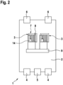
- Fig. 2 shows a second embodiment of a power module 1, which corresponds to the claimed invention.
- This embodiment essentially corresponds to the first embodiment, but the area covered by the conductor loop 8 is different.
- the conductor loop 8 essentially only covers the surface of the source 7 of the power transistor 3, and therefore does not cover the gate 14.
- the source 7 is usually the strongest heat source and the conductor loop 8 can therefore only be arranged opposite the source 7 for optimal sensitivity.
- the conductor loops can also be arranged opposite another part of the power transistor 3 or essentially opposite the entire power transistor ( Fig.1 ).
- a conductor loop can also cover several power transistors 3.
- Fig. 3 shows a third embodiment of a power module 1, for example Fig.1 or Fig. 2 in cross section through both conductor loops 8 and both power transistors 3.
- the "top" of the substrate 2 according to claim 1 is in Fig. 3 and 4 each arranged on the left.
- the conductor loops 8 here each comprise two conductor loop sections 10, 11 in two different substrate layers 12 for each power transistor 3. A meandering course of the conductor loop sections 10, 11 is shown in this view can only be guessed at, as each conductor loop (just as an example) is cut thirteen times.
- the power module 1 here comprises a first substrate 2 and a second substrate 15.
- the first substrate 2 here comprises four substrate layers 12, but two, three, five or more substrate layers 12 are also possible.
- the power transistors 3 are embedded between the two substrates 2, 15 (in a sandwich construction, so to speak).
- the conductor loop sections 10, 11 are connected between the substrate layers 12 via plated-through holes 13 (vias).
- the power transistors 3 are further connected to power wiring 16, which are arranged in particular in the 1-2 substrate layers 12 adjacent to the power transistors.
- the power wiring 16 is located in different substrate layers 12 than the conductor loops 8 for temperature measurement.
- Fig. 4 shows a fourth embodiment of a power module 1 (e.g. also one of the Fig. 1 or 2 ).
- the fourth embodiment differs from the third in that the power module 1 only has a substrate 2 with (here as an example) seven substrate layers 12.
- the power transistors 3 are embedded between the substrate layers 12 of the substrate 2.
- power wiring 16 is arranged on both sides of the power transistors 3 in the adjacent two substrate layers.
- the conductor loops 8 for temperature measurement are each in the Fig. 3 and 4 arranged in the topmost substrate layer 12 (far left) and the first inner substrate layer 12 underneath (second from the left).
Landscapes
- Physics & Mathematics (AREA)
- General Physics & Mathematics (AREA)
- Semiconductor Integrated Circuits (AREA)
- Testing Of Individual Semiconductor Devices (AREA)
- Measuring Temperature Or Quantity Of Heat (AREA)
Description
Die vorliegende Erfindung betrifft ein Leistungsmodul umfassend ein Substrat sowie mindestens einen auf einer Unterseite des Substrats angeordneten Leistungstransistor, sowie mindestens einen mit dem Substrat verbundenen Leistungsanschluss.The present invention relates to a power module comprising a substrate and at least one power transistor arranged on an underside of the substrate, as well as at least one power connection connected to the substrate.
Leistungsmodule generieren stark lokalisiert große Wärmemengen, die bei nicht ausreichender Kühlung/Herunterregelung die Lebensdauer des Leistungsmoduls stark reduzieren können. Gleichzeitig ist es schwierig, in größeren Anordnungen von Leistungsmodulen eine gezielte Kühlung je nach Bedarf bereitzustellen beziehungsweise die Temperatur der einzelnen Leistungstransistoren ohne größere Verzögerung zu messen und einen Überblick darüber zu behalten, wie stark die einzelnen Leistungsmodule bzw. Leistungshalbleiter/ Leistungstransistoren belastet werden.Power modules generate large amounts of heat in a highly localized manner, which can greatly reduce the service life of the power module if there is insufficient cooling/down regulation. At the same time, it is difficult to provide targeted cooling as required in larger arrangements of power modules or to measure the temperature of the individual power transistors without a major delay and to keep an overview of how heavily the individual power modules or power semiconductors/power transistors are loaded.
Temperaturerfassung wird in Leistungsmodulen auf unterschiedliche Weisen realisiert:
- NTC (englisch Negative Temperature Coefficient) - oder PTC (englisch Positive Temperature Coefficient) - Widerstände werden im Leistungsmodul in der Nähe der Leistungstransistoren angeordnet und über deren temperaturabhängigen Widerstand die Temperatur bestimmt,
- Erfassung der Temperatur über spezielle Bauteilanordnungen (Dioden/Widerstände) auf dem Substrat,
- Verwendung von temperatursensitiven, elektrisch messbaren Eigenschaften der Leistungstransistoren zur direkten Ermittlung der Temperatur des jeweiligen Leistungstransistors.
- NTC (English Negative Temperature Coefficient ) - or PTC (English Positive Temperature Coefficient ) - resistors are arranged in the power module near the power transistors and the temperature is determined via their temperature-dependent resistance,
- Recording the temperature via special component arrangements (diodes/resistors) on the substrate,
- Use of temperature-sensitive, electrically measurable properties of the power transistors to directly determine the temperature of the respective power transistor.
Die genannten Lösungen sind jedoch entweder ungenau und bzw. oder weisen durch ihren Abstand zur heißesten Stelle eine deutliche Zeitverzögerung in der Messung einer Temperaturspitze auf oder sie erfordern einen deutlich komplizierten Aufbau des Leistungstransistors.However, the solutions mentioned are either inaccurate and/or have a significant time delay in measuring a temperature peak due to their distance from the hottest point, or they require a significantly complicated structure of the power transistor.
Erfindungsgemäß wird ein Leistungsmodul der eingangs genannten Art zur Verfügung gestellt, wobei eine Leiterschleife zur Temperaturmessung auf einer dem Leistungstransistor gegenüberliegenden Oberseite oder inneren oder äußeren Substratschicht angeordnet ist, dadurch gekennzeichnet, dass die Leiterschleife oberhalb des Source des Leistungstransistors angeordnet ist und im Wesentlichen nur die Fläche des Source des Leistungstransistors und nicht das Gate bedeckt.According to the invention, a power module of the type mentioned is provided, wherein a conductor loop for temperature measurement is arranged on a top or inner or outer substrate layer opposite the power transistor, characterized in that the conductor loop is arranged above the source of the power transistor and essentially only the surface the source of the power transistor and not the gate.
Dies hat den Vorteil, dass die Temperatur deutlich näher als zuvor an dem mindestens einen Leistungstransistor, und damit an der Quelle der Verlustwärme, gemessen wird. Damit kann vermieden werden, dass sich ein Leistungstransistor zu stark erhitzt, bevor die Wärme durch Wärmeleitung die Leiterschleife erreicht, wie dies im Stand der Technik aufgrund des höheren Abstandes der Fall sein kann. Jedes deutliche Überschreiten der Betriebstemperatur senkt in der Regel die Lebensdauer des einzelnen Leistungstransistors.This has the advantage that the temperature is measured much closer than before to the at least one power transistor, and thus to the source of the heat loss. This can prevent a power transistor from heating up too much before the heat reaches the conductor loop through thermal conduction, as can be the case in the prior art due to the greater distance. Any significant exceeding of the operating temperature generally reduces the service life of the individual power transistor.
In Leistungsmodulen mit mehreren Leistungstransistoren kommt hinzu, dass es eine gewisse Wahrscheinlichkeit gibt, dass sich ein Leistungstransistor im Mittel häufiger und stärker erhitzt als die anderen Leistungstransistoren und damit als erster ausfällt. Außerdem kann sich ein Leistungstransistor aufgrund von Fertigungstoleranzen bei derselben Belastung höher erhitzen als ein anderer Leistungstransistor desselben Typs. Ein Ausfall eines Leistungstransistors führt aber häufig schon dazu, dass das gesamte Leistungsmodul ausgetauscht werden muss. Die erfindungsgemäße Lösung erlaubt es daher deutlich besser, die Temperaturbelastung der einzelnen Leistungstransistoren zu überwachen und gegebenenfalls gegenzusteuern, um die Gesamtlebensdauer des Leistungsmoduls zu erhöhen.In power modules with several power transistors, there is also a certain probability that one power transistor will heat up more often and more strongly than the other power transistors and will therefore be the first to fail. In addition, due to manufacturing tolerances, a power transistor may heat up higher under the same load than another power transistor of the same type. However, a failure of a power transistor often results in the entire power module having to be replaced. The solution according to the invention therefore makes it much easier to monitor the temperature load on the individual power transistors and, if necessary, counteract it in order to extend the overall service life of the To increase the power module.
Das Substrat ist vorzugsweise ein mehrschichtiges Substrat, so dass sowohl die Leistungs-, Logikverdrahtung (z.B. Steuerleitungen für Leistungstransistoren) und die zur Temperaturmessung benötigte Leiterschleife integriert werden können. Die Unterseite des Substrats kann beispielsweise die unterste Schicht des Substrats sein oder zumindest die unterste Schicht mit leitenden Elementen. Entsprechend kann die Oberseite des Substrats beispielsweise die oberste Schicht des Substrats sein, auf der leitende Elemente angeordnet sind.The substrate is preferably a multilayer substrate so that both the power and logic wiring (e.g. control lines for power transistors) and the conductor loop required for temperature measurement can be integrated. The underside of the substrate can, for example, be the lowest layer of the substrate or at least the lowest layer with conductive elements. Accordingly, the top side of the substrate can be, for example, the top layer of the substrate on which conductive elements are arranged.
Die Leiterschleife kann gemäß einer nicht beanspruchten Variante gegenüber dem gesamten Leistungstransistor oder gemäß der beanspruchten Erfindung nur einem Teil des Leistungstransistors angeordnet sein. Wenn mehrere Leistungstransistoren mit einem Substrat verbunden sind, ist vorzugsweise jeder Leistungstransistor mit einer eigenen Leiterschleife auf oberhalb des jeweiligen Leistungstransistors z.B. in einer Innenlage oder der Oberseite des Substrats versehen. Die einzelnen Leiterschleifen können dann aber mit einer gemeinsamen Auswertelektronik (zum Beispiel eine anwendungsspezifische integrierte Schaltung, ASIC, des Leistungsmoduls) verbunden sein.According to an unclaimed variant, the conductor loop can be arranged opposite the entire power transistor or, according to the claimed invention, only a part of the power transistor. If several power transistors are connected to a substrate, each power transistor is preferably provided with its own conductor loop above the respective power transistor, for example in an inner layer or the top of the substrate. The individual conductor loops can then be connected to common evaluation electronics (for example an application-specific integrated circuit, ASIC, of the power module).
Vorteilhafte Weiterbildungen der Erfindung sind in den Unteransprüchen angegeben und in der Beschreibung beschrieben.Advantageous developments of the invention are specified in the subclaims and described in the description.
Vorzugsweise weist die Leiterschleife einen mäandernden Verlauf auf. Dadurch lässt sich die Leiterstrecke unter Einfluss der erhöhten Temperatur vergrößern und damit beispielsweise ein möglichst großer Absoluteffekt auf den Widerstand der Leiterschleife erzielen.The conductor loop preferably has a meandering course. This allows the conductor distance to be increased under the influence of the increased temperature and thus, for example, to achieve the greatest possible absolute effect on the resistance of the conductor loop.
Erfindungsgemäß ist die Leiterschleife gegenüber dem Source des Leistungstransistors angeordnet. Bei einem Feldeffekttransistor ist der Source üblicherweise aufgrund der Nähe zum aktiven Gebiet des Transistors die stärkste Wärmequelle und die Leiterschleife kann für eine optimale Sensitivität daher nur gegenüber dem Source angeordnet sein. Da lokale Spitzentemperaturen zu langfristigen Schadstellen führen können, sind diese deutlich besser als die mittlere Temperatur des Leistungstransistors ein Indikator für eine problematische Überhitzung. Es ist daher vorteilhaft gezielt die Temperatur der üblicherweise heißesten Stelle des Leistungstransistors zu messen.According to the invention, the conductor loop is arranged opposite the source of the power transistor. In a field effect transistor, the source is usually the strongest heat source due to its proximity to the active region of the transistor and the conductor loop can therefore only be arranged opposite the source for optimal sensitivity. Since local peak temperatures can lead to long-term damage, these are a much better indicator of problematic overheating than the average temperature of the power transistor. It is therefore advantageous to specifically measure the temperature of the usually hottest point of the power transistor.
In einer Ausführungsform verläuft die Leiterschleife über mehrere Substratschichten. Dadurch lässt sich die Genauigkeit der Temperaturmessung erhöhen. Die Leiterschleife kann in mehreren Substratschichten einen mäandernden Verlauf aufweisen. Die Leiterschleife kann über Durchkontaktierungen (Vias) mit den verschiedenen Substratschichten verbunden sein.In one embodiment, the conductor loop runs over several substrate layers. This allows the accuracy of the temperature measurement to be increased. The conductor loop can have a meandering course in several substrate layers. The conductor loop can be connected to the various substrate layers via plated-through holes (vias).
Es ist bevorzugt, wenn auf dem Substrat mindestens zwei Leistungstransistoren angeordnet sind, wobei jeweils eine separate Leiterschleife zur Temperaturmessung oberhalb des jeweiligen Leistungstransistors in einer Innenlage oder der Oberseite des Substrats angeordnet ist. Vorzugsweise ist für jeden Leistungstransistor jeweils eine separate Leiterschleife angeordnet, also beispielsweise drei, vier, fünf, sechs oder mehr Leistungstransistoren und Leiterschleifen desselben Leistungsmoduls.It is preferred if at least two power transistors are arranged on the substrate, with a separate conductor loop for temperature measurement being arranged above the respective power transistor in an inner layer or the top of the substrate. Preferably, a separate conductor loop is arranged for each power transistor, for example three, four, five, six or more power transistors and conductor loops of the same power module.
In einer Ausführungsform weist mindestens eine Leiterschleife einen temperaturabhängigen Widerstand auf. Über den temperaturabhängigen Widerstand sind dann beispielsweise über eine Strommessung bei konstanter Spannung eine Widerstandsmessung und damit eine Temperaturmessung möglich. Der temperaturabhängige Widerstand kann ein NTC-Widerstand oder ein PTC-Widerstand sein.In one embodiment, at least one conductor loop has a temperature-dependent resistance. A resistance measurement and thus a temperature measurement are then possible via the temperature-dependent resistance, for example via a current measurement at a constant voltage. The temperature-dependent resistor can be an NTC resistor or a PTC resistor.
In einer bevorzugten Ausführungsform umfasst das Leistungsmodul mindestens eine anwendungsspezifische integrierte Schaltung (ASIC), die mit mindestens zwei Leistungstransistoren sowie mit den mindestens zwei entsprechenden Leiterschleifen verbunden ist. Die ASIC kann dann beispielsweise über eine Einzelgate-Steuerung die einzelnen Leistungstransistoren regeln, um die Temperaturbelastung der Leistungstransistoren (momentan oder über die Zeit) anzugleichen und damit die Gesamtlebensdauer oder Leistungsfähigkeit des Leistungsmoduls zu erhöhen. Die ASIC kann auf der Unterseite oder der Oberseite des Substrats angeordnet sein. Im letzteren Fall können die Leiterschleifen beispielsweise über Durchkontaktierungen (Vias) mit dem ASIC verbunden sein.In a preferred embodiment, the power module comprises at least one application-specific integrated circuit (ASIC) which is connected to at least two power transistors and to the at least two corresponding conductor loops. The ASIC can then, for example, regulate the individual power transistors via a single gate control in order to equalize the temperature load on the power transistors (currently or over time) and thus increase the overall service life or performance of the power module. The ASIC can be arranged on the bottom or top of the substrate. In the latter case, the conductor loops can be connected to the ASIC via plated-through holes (vias), for example.
In einer Ausführungsform ist die anwendungsspezifische integrierte Schaltung so eingerichtet, dass sie die Auslastung der mindestens zwei Leistungstransistoren so steuert, dass die über die Leiterschleifen gemessene Temperatur möglichst gleich ist. Diese Lösung ist möglichst einfach, da es nicht unbedingt notwendig ist, eine "Temperaturhistorie" für die einzelnen Leistungstransistoren zu speichern, um zu entscheiden, welcher Leistungstransistor mehr belastet werden kann und soll. Es kann dann einfach im Betrieb der oder die Leistungstransistoren heruntergeregelt werden, deren Temperaturen oberhalb eines oberen Temperaturschwellenwerts (einer problematischen Temperatur) liegt und diejenigen Leistungstransistoren hochgeregelt werden, deren Temperatur unterhalb eines unteren Temperaturschwellenwerts (einer unproblematischen Temperatur) liegt. Die Verwendung von zwei verschiedenen Schwellenwerten kann die Regelung dabei stabilisieren, um häufiges Hochregeln und Herunterregeln zu vermeiden.In one embodiment, the application-specific integrated circuit is set up to control the utilization of the at least two power transistors controlled in such a way that the temperature measured across the conductor loops is as equal as possible. This solution is as simple as possible because it is not absolutely necessary to store a "temperature history" for the individual power transistors in order to decide which power transistor can and should be loaded more. It is then possible to simply turn down the power transistor(s) during operation whose temperatures are above an upper temperature threshold (a problematic temperature) and turn up those power transistors whose temperature is below a lower temperature threshold (a non-problematic temperature). The use of two different threshold values can stabilize the control to avoid frequent up-regulation and down-regulation.
Es ist bevorzugt, wenn das Substrat eine mehrschichtige Niedertemperatur-Einbrand-Keramik (engl. Low Temperature Cofired Ceramics, LTCC) ist oder umfasst. Bei einem derartigen Substrat ist es problemlos möglich, auf der die Leistungstransistoren umfassenden Unterseite gegenüberliegenden Oberseite bzw. in den Innenlagen zusätzliche Leiterschleifen zur Temperaturmessung vorzusehen, ohne dass dies die Fertigungsprozesse deutlich erschwert.It is preferred if the substrate is or comprises a multilayer low temperature cofired ceramics (LTCC). With such a substrate, it is easily possible to provide additional conductor loops for temperature measurement on the underside containing the power transistors opposite the upper side or in the inner layers, without this significantly complicating the manufacturing processes.
In einer Ausführungsform erfolgt die Temperaturmessung in mindestens einer Leiterschleife über eine Vierpunktmessung oder einen Band-Ende-Abgleich. Diese Messmethoden erhöhen die Genauigkeit der Messung, ohne den Aufbau deutlich zu erschweren. Es sind dann aber gegebenenfalls ein anderer Verlauf der Leiterschleife und entsprechende Anschlüsse an die Auswerteelektronik (zum Beispiel lokaler ASIC) erforderlich.In one embodiment, the temperature measurement is carried out in at least one conductor loop via a four-point measurement or an end-of-band adjustment. These measuring methods increase the accuracy of the measurement without significantly complicating the setup. However, a different route of the conductor loop and corresponding connections to the evaluation electronics (for example local ASIC) may then be required.
In einer Ausführungsform sind mehrere Leiterschleifen in unterschiedlichen Substratschichten angeordnet und in Reihe geschaltet. Dadurch lässt sich die Länge der Leiterschleife im heißen Bereich zu maximieren. Hierdurch wird die Widerstandsänderung bei einer Temperaturänderung und somit die Sensitivität der Temperaturmessung erhöht.In one embodiment, several conductor loops are arranged in different substrate layers and connected in series. This allows the length of the conductor loop in the hot area to be maximized. This increases the change in resistance when the temperature changes and thus the sensitivity of the temperature measurement.
In einer Ausführungsform umfasst das Leistungsmodul mindestens zwei Substrate. Eine Leistungsverdrahtung und die Leiterschleifen zur Temperaturmessung können dabei in einem der beiden Substrate (z. B. in unterschiedlichen Substratschichten) angeordnet sein.In one embodiment, the power module includes at least two substrates. A power wiring and the conductor loops for Temperature measurements can be arranged in one of the two substrates (e.g. in different substrate layers).
In einer Ausführungsform umfasst das Leistungsmodul mehrere zwischen Substratschichten eingebettete Leistungshalbleiter. Hier umfasst das Leistungsmodul vorzugsweise nur ein Substrat mit mehreren Substratschichten. Die Leistungshalbleiter können in einer inneren Substratschicht angeordnet sein und von beiden Seiten zwischen weiteren Substratschichten eingebettet bzw. gesandwicht sein.In one embodiment, the power module comprises a plurality of power semiconductors embedded between substrate layers. Here the power module preferably comprises only one substrate with several substrate layers. The power semiconductors can be arranged in an inner substrate layer and embedded or sandwiched between further substrate layers on both sides.
In einer Ausführungsform umfasst das Leistungsmodul mehrere zwischen zwei Substraten eingebettete Leistungshalbleiter, wobei in mindestens einem der Substrate Leiterschleifen zur Temperaturmessung angeordnet sind. Diese Leistungshalbleiter sind bevorzugt "kopfüber" in dem Substrat eingebettet, so dass sich die Source Fläche auf der Unterseite befindet. In diesem Fall wäre die Mäanderstruktur "unterhalb" der Leistungstransistoren (z. B. MOSFETs) angeordnet. Zusätzlich zu dem Leistungstransistor umfasst das Leistungsmodul also auch mehrere Leistungshalbleiter, dessen Temperatur ebenfalls mit einer oder mehreren Leiterschleifen gemessen werden kann. Die Leistungshalbleiter können beispielweise Leistungsdioden, Thyristoren oder Triacs sein.In one embodiment, the power module comprises a plurality of power semiconductors embedded between two substrates, with conductor loops for temperature measurement being arranged in at least one of the substrates. These power semiconductors are preferably embedded "upside down" in the substrate, so that the source surface is on the underside. In this case, the meander structure would be arranged "below" the power transistors (e.g. MOSFETs). In addition to the power transistor, the power module also includes several power semiconductors, the temperature of which can also be measured with one or more conductor loops. The power semiconductors can be, for example, power diodes, thyristors or triacs.
In einer Ausführungsform umfasst das Leistungsmodul mindestens einen Leistungshalbleiter, wobei eine weitere Leiterschleife zur Temperaturmessung auf einer dem Leistungshalbleiter gegenüberliegenden Oberseite des Substrats angeordnet ist. Auch hier umfasst das Leistungsmodul also zusätzlich zu dem Leistungstransistor auch mindestens einen Leistungshalbleiter, dessen Temperatur ebenfalls mit einer Leiterschleife gemessen werden kann. Der Leistungshalbleiter kann beispielweise eine Leistungsdiode, ein Thyristor oder ein Triac sein.In one embodiment, the power module comprises at least one power semiconductor, with a further conductor loop for temperature measurement being arranged on an upper side of the substrate opposite the power semiconductor. Here too, in addition to the power transistor, the power module also includes at least one power semiconductor, the temperature of which can also be measured with a conductor loop. The power semiconductor can be, for example, a power diode, a thyristor or a triac.
In Vergleich zu klassischen Anordnungen (NTC) der Leiterschleife neben einem Leistungshalbleiter auf einem unteren Substrat ist die Leiterschleife erfindungsgemäß sehr nahe am Hotspot und nicht im Kühlpfad angeordnet. Hierdurch kann die Maximaltemperatur des Leistungshalbleiters mit einer hohen Genauigkeit gemessen werden.In comparison to classic arrangements (NTC) of the conductor loop next to a power semiconductor on a lower substrate, according to the invention the conductor loop is arranged very close to the hotspot and not in the cooling path. This allows the maximum temperature of the power semiconductor to be measured with a high level of accuracy.
Bevorzugt wird unter einer Außenlage eines Substrates die oberste und unterste Schicht eines Substrates verstanden. Außenlagen haben daher auf einer Seite keinen Kontakt zu weiteren Substratschichten.An outer layer of a substrate is preferably understood to mean the top and bottom layers of a substrate. Outer layers therefore have no contact with other substrate layers on one side.
Bevorzugt wird unter einer inneren Substratschicht beziehungsweise einer sogenannten Innenlage eine Substratschicht verstanden, welche zwischen zwei Substratlagen liegt. Dementsprechend hat ein Substrat immer mindestens eine Außenlage aber nicht zwingend eine Innenlage. Für eine Innenlage sind mindestens drei Substratschichten, also zwei Außenlagen (Top, Botton) und eine Innenlage zwischen diesen beiden Außenlagen erforderlich.An inner substrate layer or a so-called inner layer is preferably understood to mean a substrate layer which lies between two substrate layers. Accordingly, a substrate always has at least one outer layer but not necessarily an inner layer. For an inner layer, at least three substrate layers are required, i.e. two outer layers (top, bottom) and an inner layer between these two outer layers.
Ausführungsbeispiele der Erfindung werden anhand der einzigen Zeichnung und der nachfolgenden Beschreibung näher erläutert. Es zeigt:
-
Figur 1 eine erste Ausführungsform eines Leistungsmoduls in einer Ansicht von der Oberseite des Leistungsmoduls. -
Figur 2 -
Figur 3 -
Figur 4 eine vierte Ausführungsform eines Leistungsmoduls in Querschnittsansicht.
-
Figure 1 a first embodiment of a power module in a view from the top of the power module. -
Figure 2 a second embodiment of a power module in a view from the top of the power module. -
Figure 3 a third embodiment of a power module in a cross-sectional view. -
Figure 4 a fourth embodiment of a power module in a cross-sectional view.
In
Das Leistungsmodul 1 umfasst fünf mit dem Substrat 2 verbundene Leistungsanschlüsse 4, 5, 6. Die Leistungsanschlüsse 4, 5, 6 können beispielsweise mit je einem Source 7 und einem Gate 14 (jeweils gestrichelt eingezeichnet, da auf der Unterseite des Substrats oder in das Substrat eingebettet) je eines Leistungstransistors 3 verbunden sein. Die Leistungsanschlüsse 4 können beispielsweise eine Versorgungsspannung liefern, der Leistungsanschluss 5 kann beispielsweise eine Masse bereitstellen und die Leistungsanschlüsse 6 können Phasenanschlüsse sein. Eine entsprechende Steuerelektronik auf dem Substrat 2 ist hier der Einfachheit halber nicht dargestellt.The power module 1 includes five
Erfindungsgemäß sind Leiterschleifen 8 zur Temperaturmessung auf einer den Leistungstransistoren 3 gegenüberliegenden Oberseite des Substrats 2 angeordnet.According to the invention,
Die Leiterschleifen 8 weisen einen mäandernden Verlauf auf, wodurch sich die Leiterstrecke unter Einfluss der erhöhten Temperatur vergrößern und damit beispielsweise ein möglichst großer Absoluteffekt auf den Widerstand der Leiterschleifen 8 erzielen lässt.The
Die Leiterschleifen 8 sind hier in Wesentlichen gegenüber der gesamten Fläche des jeweiligen Leistungstransistors 3 angeordnet.. Die Leiterschleifen 8 können aber auch eine größere Fläche als die Fläche des jeweiligen Leistungstranstors 3 abdecken (z. B. eine um 10-100% größere Fläche) um die gemessene absolute Widerstandsänderung zu vergrößern.The
Die Leiterschleife 8 kann über mehrere Lagen mit Durchkontaktierungen (Vias) verbunden und geführt sein um die Länge im heißen Bereich über dem Leistungstransistor (z.B. MOSFET) zu maximieren. Hierdurch kann die Widerstandsänderung der Leiterschleife erhöht und damit die Sensitivität der Erfindung verbessert werden.The
Das Leistungsmodul 1 umfasst eine anwendungsspezifische integrierte Schaltung 9 (ASIC), die mit beiden (allen) Leistungstransistoren 3 sowie mit den zwei (allen) entsprechenden Leiterschleifen 8 verbunden ist. Die ASIC 9 kann dann beispielsweise über eine Einzelgate-Steuerung die einzelnen Leistungstransistoren 3 regeln, um die Temperaturbelastung der Leistungstransistoren 3 (momentan oder über die Zeit) anzugleichen und damit die Gesamtlebensdauer des Leistungshalbleiters zu erhöhen. Die ASIC 9 kann auf der Unterseite oder der Oberseite des Substrats angeordnet sein (hier beispielsweise auf der Oberseite). Im letzteren Fall können die Leiterschleifen 8 beispielsweise über Durchkontaktierungen (Vias) mit der ASIC 9 verbunden sein. Die Leiterschleifen 8 sind mit der ASIC 9 hier nur beispielhaft an den beiden Enden der Leiterschleifen 8 verbunden, aber es sind auch andere Anschlussarten möglich (zum Beispiel für eine Vierpunktmessung), um eine höhere Genauigkeit der Widerstandsmessung zu ermöglichen.The power module 1 includes an application-specific integrated circuit 9 (ASIC), which is connected to both (all)
Bei einem Feldeffekttransistor ist der Source 7 üblicherweise die stärkste Wärmequelle und die Leiterschleife 8 kann für eine optimale Sensitivität daher nur gegenüber dem Source 7 angeordnet sein. Die Leiterschleifen können aber auch alternativ, gemäß nicht beanspruchten Alternativen, gegenüber einem anderen Teil des Leistungstransistors 3 oder im Wesentlichen gegenüber dem gesamten Leistungstransistor angeordnet sein (
Die Leiterschleifen 8 umfassen hier je zwei Leiterschleifenabschnitte 10, 11 in zwei verschiedenen Substratschichten 12 für jeden Leistungstransistor 3. Ein mäandernder Verlauf der Leiterschleifenabschnitte 10, 11 ist in dieser Ansicht nur zu erahnen, da jede Leiterschleife (lediglich beispielhaft) dreizehnfach geschnitten wird. Das Leistungsmodul 1 umfasst hier ein erstes Substrat 2 und ein zweites Substrat 15. Das erste Substrat 2 umfasst hier vier Substratschichten 12, es sind aber auch zwei, drei, fünf oder mehr Substratschichten 12 möglich. Die Leistungstransistoren 3 sind zwischen den zwei Substraten 2, 15 eingebettet (gewissermaßen in Sandwichbauweise).The
Die Leiterschleifenabschnitte 10, 11 sind über Durchkontaktierungen 13 (Vias) zwischen den Substratschichten 12 verbunden. Die Leistungstransistoren 3 sind weiterhin mit Leistungsverdrahtungen 16 verbunden, die insbesondere in der an die Leistungstransistoren angrenzenden 1-2 Substratschichten 12 angeordnet sind. Die Leistungsverdrahtungen 16 befinden sich dabei in unterschiedlichen Substratschichten 12 als die Leiterschleifen 8 zur Temperaturmessung.The
Die Leiterschleifen 8 zur Temperaturmessung sind aber jeweils in den
Claims (14)
- Power module (1) comprising a preferably multilayered substrate (2) and at least one power transistor (3) arranged on an underside of the substrate (2), and at least one power connection (4, 5, 6) connected to the substrate (2),wherein a conductor loop (8) for temperature measurement is arranged on a top side or inner or outer substrate layer (12) opposite the power transistor (3),characterized in that the conductor loop (8) is arranged above the source (7) of the power transistor (3) and covers substantially only the area of the source (7) of the power transistor (3) and not the gate (14).
- Power module (1) according to Claim 1, wherein the conductor loop (8) has a meandering course.
- Power module (1) according to either of the preceding claims, wherein the conductor loop (8) extends over a plurality of substrate layers (12).
- Power module (1) according to any of the preceding claims, wherein at least two power transistors (3) are arranged on the substrate (2), wherein in each case a separate conductor loop (8) for temperature measurement is arranged above the respective power transistor (3) in an inner substrate layer (12) or the top side of the substrate (2).
- Power module (1) according to any of the preceding claims, wherein at least one conductor loop (8) has a temperature-dependent resistance.
- Power module (1) according to either of Claims 4 and 5, comprising at least one application-specific integrated circuit (9) which is connected to at least two power transistors (3) and to the at least two corresponding conductor loops (8).
- Power module (1) according to Claim 6, wherein the application-specific integrated circuit (9) is configured such that it controls the capacity utilization of the at least two power transistors (3) such that the temperature measured by way of the conductor loops (8) is as far as possible identical.
- Power module (1) according to any of the preceding claims, wherein the substrate (2) comprises a multilayered low-temperature cofired ceramic.
- Power module (1) according to any of the preceding claims, wherein the temperature measurement in at least one conductor loop (8) takes place by way of a four-point measurement or an end-of-line calibration.
- Power module (1) according to any of the preceding claims, wherein a plurality of conductor loops (8) are arranged in different substrate layers (12) and connected in series.
- Power module (1) according to any of the preceding claims, which comprises at least two substrates (2, 15).
- Power module (1) according to any of the preceding claims, which comprises a plurality of power semiconductors embedded between substrate layers (12).
- Power module (1) according to Claim 11 or 12, which comprises a plurality of power semiconductors embedded between two substrates (2, 15), wherein conductor loops (8) for temperature measurement are arranged in at least one of the substrates (2, 15).
- Power module (1) according to any of the preceding claims, comprising at least one power semiconductor, wherein a further conductor loop (8) for temperature measurement is arranged on a top side of the substrate (2) opposite the power semiconductor.
Applications Claiming Priority (2)
| Application Number | Priority Date | Filing Date | Title |
|---|---|---|---|
| DE102020203918.6A DE102020203918A1 (en) | 2020-03-26 | 2020-03-26 | Power module |
| PCT/EP2021/057382 WO2021191187A1 (en) | 2020-03-26 | 2021-03-23 | Power module |
Publications (2)
| Publication Number | Publication Date |
|---|---|
| EP4127633A1 EP4127633A1 (en) | 2023-02-08 |
| EP4127633B1 true EP4127633B1 (en) | 2024-02-14 |
Family
ID=75339684
Family Applications (1)
| Application Number | Title | Priority Date | Filing Date |
|---|---|---|---|
| EP21715797.3A Active EP4127633B1 (en) | 2020-03-26 | 2021-03-23 | Power module |
Country Status (6)
| Country | Link |
|---|---|
| US (1) | US20230082076A1 (en) |
| EP (1) | EP4127633B1 (en) |
| JP (1) | JP2023519835A (en) |
| CN (1) | CN115335670A (en) |
| DE (1) | DE102020203918A1 (en) |
| WO (1) | WO2021191187A1 (en) |
Family Cites Families (3)
| Publication number | Priority date | Publication date | Assignee | Title |
|---|---|---|---|---|
| DE19522126C2 (en) | 1995-06-19 | 1999-01-28 | Hella Kg Hueck & Co | Electronic load switch for a motor vehicle, for example flasher unit |
| DE102014208526B4 (en) | 2014-05-07 | 2020-01-30 | Infineon Technologies Ag | ELECTRONICS ASSEMBLY |
| US10260961B2 (en) * | 2015-12-21 | 2019-04-16 | Intel Corporation | Integrated circuit packages with temperature sensor traces |
-
2020
- 2020-03-26 DE DE102020203918.6A patent/DE102020203918A1/en active Pending
-
2021
- 2021-03-23 EP EP21715797.3A patent/EP4127633B1/en active Active
- 2021-03-23 US US17/793,012 patent/US20230082076A1/en active Pending
- 2021-03-23 WO PCT/EP2021/057382 patent/WO2021191187A1/en unknown
- 2021-03-23 JP JP2022557688A patent/JP2023519835A/en active Pending
- 2021-03-23 CN CN202180024572.1A patent/CN115335670A/en active Pending
Also Published As
| Publication number | Publication date |
|---|---|
| US20230082076A1 (en) | 2023-03-16 |
| JP2023519835A (en) | 2023-05-15 |
| CN115335670A (en) | 2022-11-11 |
| EP4127633A1 (en) | 2023-02-08 |
| DE102020203918A1 (en) | 2021-09-30 |
| WO2021191187A1 (en) | 2021-09-30 |
Similar Documents
| Publication | Publication Date | Title |
|---|---|---|
| DE102010029147B4 (en) | Method for determining the temperature of a power semiconductor | |
| DE102014106695B4 (en) | POWER TRANSISTOR WITH INTEGRATED TEMPERATURE SENSOR ELEMENT, POWER TRANSISTOR CIRCUIT, METHOD FOR OPERATING A POWER TRANSISTOR AND METHOD FOR OPERATING A POWER TRANSISTOR CIRCUIT | |
| DE102018131999B4 (en) | POWER MODULE AND POWER CONVERTER | |
| EP3224631A1 (en) | Method for determining a deterioration of power semiconductor modules as well as a device and circuit arrangement | |
| DE112013007670T5 (en) | Semiconductor device | |
| DE102004062214B4 (en) | Semiconductor device with temperature detection function | |
| EP0780672B1 (en) | Field effect controllable semiconductor device with temperature sensor | |
| DE102008026545A1 (en) | Semiconductor subassemblies with interconnections and method of manufacturing the same | |
| DE102011050122A1 (en) | Component useful as a circuit breaker for an inverter, comprises a MOSFET having a gate terminal and a source terminal, a first diode for measuring a junction temperature of the MOSFET, and a second diode and/or a third diode | |
| DE102008035993B4 (en) | The power semiconductor module | |
| DE102019213509A1 (en) | Semiconductor device | |
| WO2009141347A1 (en) | Operating temperature measurement for an mos power component, and mos component for carrying out the method | |
| EP4127633B1 (en) | Power module | |
| DE102011004353A1 (en) | Circuit board of electric energy store e.g. traction battery of electric vehicle, has temperature sensor positioned adjacent to one of conductor ends | |
| WO2009141350A2 (en) | Location-related adjustment of the operating temperature distribution or power distribution of a semiconductor power component, and component for carrying out said method | |
| DE102014201781A1 (en) | ARRANGEMENT AND METHOD FOR MEASURING CHIP TEMPERATURE IN A POWER SEMICONDUCTOR MODULE | |
| DE102008044411A1 (en) | Integrated circuit with a power MOS transistor | |
| EP1573917B1 (en) | Semiconductor circuit arrangement for controlling a high voltage or a high intensity current | |
| WO2022184764A1 (en) | Power module with detection of aging | |
| DE19920505B4 (en) | Inverter with temperature balancing | |
| DE4401956A1 (en) | Power semiconductor device, esp. MOSFET with temp. sensor | |
| EP2254215B1 (en) | Circuit arrangement | |
| DE102021208424A1 (en) | Power arrangement with temperature control using gate shaping | |
| DE102012009746B4 (en) | Method for checking the thermal coupling between a semiconductor device and a heat sink | |
| DE2329872A1 (en) | THYRISTOR |
Legal Events
| Date | Code | Title | Description |
|---|---|---|---|
| STAA | Information on the status of an ep patent application or granted ep patent |
Free format text: STATUS: UNKNOWN |
|
| STAA | Information on the status of an ep patent application or granted ep patent |
Free format text: STATUS: THE INTERNATIONAL PUBLICATION HAS BEEN MADE |
|
| PUAI | Public reference made under article 153(3) epc to a published international application that has entered the european phase |
Free format text: ORIGINAL CODE: 0009012 |
|
| STAA | Information on the status of an ep patent application or granted ep patent |
Free format text: STATUS: REQUEST FOR EXAMINATION WAS MADE |
|
| 17P | Request for examination filed |
Effective date: 20221026 |
|
| AK | Designated contracting states |
Kind code of ref document: A1 Designated state(s): AL AT BE BG CH CY CZ DE DK EE ES FI FR GB GR HR HU IE IS IT LI LT LU LV MC MK MT NL NO PL PT RO RS SE SI SK SM TR |
|
| DAV | Request for validation of the european patent (deleted) | ||
| DAX | Request for extension of the european patent (deleted) | ||
| GRAP | Despatch of communication of intention to grant a patent |
Free format text: ORIGINAL CODE: EPIDOSNIGR1 |
|
| STAA | Information on the status of an ep patent application or granted ep patent |
Free format text: STATUS: GRANT OF PATENT IS INTENDED |
|
| INTG | Intention to grant announced |
Effective date: 20230929 |
|
| GRAS | Grant fee paid |
Free format text: ORIGINAL CODE: EPIDOSNIGR3 |
|
| GRAA | (expected) grant |
Free format text: ORIGINAL CODE: 0009210 |
|
| STAA | Information on the status of an ep patent application or granted ep patent |
Free format text: STATUS: THE PATENT HAS BEEN GRANTED |
|
| AK | Designated contracting states |
Kind code of ref document: B1 Designated state(s): AL AT BE BG CH CY CZ DE DK EE ES FI FR GB GR HR HU IE IS IT LI LT LU LV MC MK MT NL NO PL PT RO RS SE SI SK SM TR |
|
| REG | Reference to a national code |
Ref country code: GB Ref legal event code: FG4D Free format text: NOT ENGLISH |
|
| REG | Reference to a national code |
Ref country code: CH Ref legal event code: EP |
|
| REG | Reference to a national code |
Ref country code: DE Ref legal event code: R096 Ref document number: 502021002691 Country of ref document: DE |
|
| REG | Reference to a national code |
Ref country code: IE Ref legal event code: FG4D Free format text: LANGUAGE OF EP DOCUMENT: GERMAN |