EP4124641A1 - Integrated circuit package with surface modified liquid metal spheres and method of making - Google Patents
Integrated circuit package with surface modified liquid metal spheres and method of making Download PDFInfo
- Publication number
- EP4124641A1 EP4124641A1 EP22186026.5A EP22186026A EP4124641A1 EP 4124641 A1 EP4124641 A1 EP 4124641A1 EP 22186026 A EP22186026 A EP 22186026A EP 4124641 A1 EP4124641 A1 EP 4124641A1
- Authority
- EP
- European Patent Office
- Prior art keywords
- package
- die
- liquid metal
- monomer
- thermal interface
- Prior art date
- Legal status (The legal status is an assumption and is not a legal conclusion. Google has not performed a legal analysis and makes no representation as to the accuracy of the status listed.)
- Pending
Links
Images



Classifications
-
- C—CHEMISTRY; METALLURGY
- C09—DYES; PAINTS; POLISHES; NATURAL RESINS; ADHESIVES; COMPOSITIONS NOT OTHERWISE PROVIDED FOR; APPLICATIONS OF MATERIALS NOT OTHERWISE PROVIDED FOR
- C09K—MATERIALS FOR MISCELLANEOUS APPLICATIONS, NOT PROVIDED FOR ELSEWHERE
- C09K5/00—Heat-transfer, heat-exchange or heat-storage materials, e.g. refrigerants; Materials for the production of heat or cold by chemical reactions other than by combustion
- C09K5/08—Materials not undergoing a change of physical state when used
- C09K5/10—Liquid materials
-
- C—CHEMISTRY; METALLURGY
- C09—DYES; PAINTS; POLISHES; NATURAL RESINS; ADHESIVES; COMPOSITIONS NOT OTHERWISE PROVIDED FOR; APPLICATIONS OF MATERIALS NOT OTHERWISE PROVIDED FOR
- C09K—MATERIALS FOR MISCELLANEOUS APPLICATIONS, NOT PROVIDED FOR ELSEWHERE
- C09K5/00—Heat-transfer, heat-exchange or heat-storage materials, e.g. refrigerants; Materials for the production of heat or cold by chemical reactions other than by combustion
- C09K5/08—Materials not undergoing a change of physical state when used
- C09K5/14—Solid materials, e.g. powdery or granular
-
- H—ELECTRICITY
- H10—SEMICONDUCTOR DEVICES; ELECTRIC SOLID-STATE DEVICES NOT OTHERWISE PROVIDED FOR
- H10W—GENERIC PACKAGES, INTERCONNECTIONS, CONNECTORS OR OTHER CONSTRUCTIONAL DETAILS OF DEVICES COVERED BY CLASS H10
- H10W40/00—Arrangements for thermal protection or thermal control
- H10W40/20—Arrangements for cooling
- H10W40/25—Arrangements for cooling characterised by their materials
- H10W40/257—Arrangements for cooling characterised by their materials having a heterogeneous or anisotropic structure, e.g. powder or fibres in a matrix, wire mesh or porous structures
-
- H—ELECTRICITY
- H10—SEMICONDUCTOR DEVICES; ELECTRIC SOLID-STATE DEVICES NOT OTHERWISE PROVIDED FOR
- H10W—GENERIC PACKAGES, INTERCONNECTIONS, CONNECTORS OR OTHER CONSTRUCTIONAL DETAILS OF DEVICES COVERED BY CLASS H10
- H10W72/00—Interconnections or connectors in packages
- H10W72/071—Connecting or disconnecting
-
- H—ELECTRICITY
- H10—SEMICONDUCTOR DEVICES; ELECTRIC SOLID-STATE DEVICES NOT OTHERWISE PROVIDED FOR
- H10W—GENERIC PACKAGES, INTERCONNECTIONS, CONNECTORS OR OTHER CONSTRUCTIONAL DETAILS OF DEVICES COVERED BY CLASS H10
- H10W40/00—Arrangements for thermal protection or thermal control
- H10W40/20—Arrangements for cooling
- H10W40/22—Arrangements for cooling characterised by their shape, e.g. having conical or cylindrical projections
-
- H—ELECTRICITY
- H10—SEMICONDUCTOR DEVICES; ELECTRIC SOLID-STATE DEVICES NOT OTHERWISE PROVIDED FOR
- H10W—GENERIC PACKAGES, INTERCONNECTIONS, CONNECTORS OR OTHER CONSTRUCTIONAL DETAILS OF DEVICES COVERED BY CLASS H10
- H10W40/00—Arrangements for thermal protection or thermal control
- H10W40/20—Arrangements for cooling
- H10W40/25—Arrangements for cooling characterised by their materials
- H10W40/251—Organics
-
- H—ELECTRICITY
- H10—SEMICONDUCTOR DEVICES; ELECTRIC SOLID-STATE DEVICES NOT OTHERWISE PROVIDED FOR
- H10W—GENERIC PACKAGES, INTERCONNECTIONS, CONNECTORS OR OTHER CONSTRUCTIONAL DETAILS OF DEVICES COVERED BY CLASS H10
- H10W40/00—Arrangements for thermal protection or thermal control
- H10W40/20—Arrangements for cooling
- H10W40/25—Arrangements for cooling characterised by their materials
- H10W40/258—Metallic materials
-
- H—ELECTRICITY
- H10—SEMICONDUCTOR DEVICES; ELECTRIC SOLID-STATE DEVICES NOT OTHERWISE PROVIDED FOR
- H10W—GENERIC PACKAGES, INTERCONNECTIONS, CONNECTORS OR OTHER CONSTRUCTIONAL DETAILS OF DEVICES COVERED BY CLASS H10
- H10W90/00—Package configurations
Definitions
- One or more integrated circuits can be provided on or within a module or integrated circuit package.
- the package can be a multi-chip module or a single chip package.
- Each of the one or more ICs is generally provided on a die that is connected by fine wires or by solder bumps to a package substrate.
- the single chip package or multichip module often includes a cover or other protective structure that covers the one or more ICs.
- integrated circuit or IC package as used herein includes single chip packages and multi-chip modules.
- a package comprising:
- the one or more die are attached to the package substrate.
- the one or more die are attached to the package substrate by solder balls.
- the one or more die are attached using a flip chip configuration.
- the thermal interface material is disposed between the cover and the one or more die.
- the thermal interface material is comprised of a polymer comprising the first monomer and wherein the polymer is bonded to the liquid metal by an organometallic bond, coordinate, or a covalent bond.
- the cover is attached to the package substrate and the one or more die are attached to the package substrate.
- the thermal interface material is comprised of surface modified liquid spheres.
- the thermal interface material is comprised of a polymer comprised of the first monomer and a second monomer.
- the second monomer is bonded to the first monomer.
- a method is provided of fabricating an integrated circuit package, the method comprising:
- the polymerized material is a polymer matrix and at least one of the monomers comprises a silicon monomer.
- the liquid metal is liquid at room temperature.
- the liquid metal is shaped in spheres.
- the polymerized material is a polymer matrix and the spheres are evenly distributed in the polymer matrix.
- the polymeric matrix comprises two or more monomers.
- the modified liquid-metal in the polymeric matrix comprises surface modified liquid metal spheres.
- the surface modified liquid metal spheres are evenly distributed in the polymer matrix.
- the monomer comprises silicon and is an adhesion promoter.
- devices can be provided in IC packages (e.g., as single chip packages having a single IC or as a system in package (SiP) having two or more ICs or dies in a package (e.g., a multi-chip module) according to various exemplary embodiments.
- IC packages and methods related to IC packages utilize surface modified liquid metal spheres to provide a robust liquid metal polymer composite thermal interface material in some embodiments.
- a liquid metal polymer composite thermal interface material provides superior heat extraction.
- the liquid metal polymer composite thermal interface material provides a more heat conductive path to a heat sink or heat spreader in some embodiments.
- the thermal interface material is configured to be thermally and mechanically reliable and can be used in higher power IC devices.
- copolymerization of surface modified liquid-metal and silicon monomers provides a robust material with uniform distribution of thermally conductive liquid-metal in the polymer matrix.
- Liquid metal has high thermal conductivity but generally exhibits poor reliability.
- Liquid metal loaded polymers have good thermal conductivity and reliability but generally lack homogeneity - liquid metal is severely depleted at the edges due to insufficient interaction between liquid metal and polymer.
- Silicon monomers organo-metallically or covalently bonded to the liquid metal create copolymerized silicon monomers that provide strong bonding and overcome the limitations of certain conventional liquid metal loaded polymers in some embodiments.
- a package includes a one or more die, a package substrate, a thermal interface material, and a cover.
- the cover is disposed over or above the one or more die.
- the thermal interface material includes a surface modified metal and a silicon monomer.
- Some embodiments relate to a method of fabricating an integrated circuit package.
- the method includes attaching a die to a substrate, providing a polymerized material including two monomers and a liquid metal.
- the liquid metal is bonded by a covalent bond or organometallic bond to at least one of the two monomers.
- the method also includes providing a cover over the die, and the polymerized material is disposed in at least a region between the cover and the die.
- thermal interface material for an integrated circuit package.
- the thermal interface material includes a polymer matrix comprising copolymerized modified liquid-metal and a silicon monomer.
- thermal interface material for an integrated circuit package.
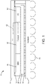
- an integrated circuit package 10 (e.g., system in package (SiP)) includes cover 12 (e.g., a lid), a package substrate 14, an interconnect board 16, a die 30, a die 32, a die 34, and thermal interface material 48.
- Integrated circuit package 10 is a single die package or a multiple die package in some embodiments.
- Integrated circuit package 10 is configured for side-by-side die packaging, three dimensional packaging, embedded packaging, and other configurations for containing one or more of die 30, 32, and 34.
- Integrated circuit package 10 and components thereof can have a variety thicknesses and sizes depending on die area and system criteria.
- a set 28 of solder balls can interconnect board 16 to die 30, 32, and 34 in some embodiments.
- the die 30, 32, and 34 are coupled to the interconnect board 16 in a flip chip configuration in some embodiments.
- the set 28 of solder balls can be pins, solder bumps, wires, or other structures for coupling die 30, 32, and 34 to interconnect board 16 or other circuit boards, other devices, or substrates in some embodiments.
- die 30, 32, and 34 are coupled directly to the package substrate 14 by solder balls, pins, solder bump, wires, or other structures.
- Die 30, 32 and 34 can be any type of electronic device including a memory, a processor, a radio frequency circuit, programmable logic device, application specific integrated circuit (ASIC), or other logic device.
- die 30 is a DRAM or high bandwidth memory (HBM) chip
- die 32 is a computer or processor chip
- die 34 is an input/output module.
- Die 30, 32, and 34 are coupled to the substrate 14 via set 28 of solder balls and interconnect board 16 in some embodiments.
- a set 18 of solder balls can be provided on a bottom of substrate 14 for coupling to circuit boards or other components.
- the set 18 of solder balls can be pins, solder bump, wires, or other structures.
- the substrate 14 and interconnect board 16 can be any type of IC package circuit board.
- interconnect board 16 and package substrate 14 are ceramic boards.
- interconnect board 16 and package substrate 14 are alumina, aluminum nitride or beryllium oxide, flex, or fiberglass circuit boards.
- Cover 12 is a metal, metal composite, or ceramic material in some embodiments. Cover 12 is adhered to substrate 14 in some embodiments. Cover 12 can be coupled to or integrated with a heat sink or heat spreader for heat dissipation in some embodiments. Cover 12 is tungsten, copper, copper-diamond, silver-diamond, aluminum, silicon carbide, gold, nickel, and alloys thereof in some embodiments.
- thermal interface material 48 is disposed in a region between cover 12 and at least one of die 30, 32, and 34. An enlarged area 62 of integrated circuit package 10 is shown in FIG. 2 .
- Thermal interface material 48 can be provided in other regions where thermal conductivity is desired.
- thermal interface material 48 is configured for heat dissipation and is an insulating material.
- thermal interface material 48 includes a liquid metal material disposed in a polymerized matrix. The liquid metal material is liquid phase eutectic gallium-indium micro droplets in some embodiments.
- thermal interface material 48 is configured for homogeneity in the polymerized matrix and is not significantly depleted at edges of the polymerized matrix. Arrows 1 and 2 show heat dissipation through the die 32 and the thermal interface material 48 to the cover or cover 12.
- a flow 200 is performed to fabricate the integrated circuit package 10 with the thermal interface material 48.
- Flow 200 exemplary only and is not limited to operations performed in a particular order.
- one or more die are attached to interconnect board 16 or other circuit board/substrate for housing die.
- the interconnect board16 can be a single package substrate which is part of the integrated circuit package 10 or can be one of two or more circuit boards in the integrated circuit package 10.
- the interconnect board16 is an intermediate board, interposer, or the top most or bottom most substrate (e.g., package substrate 14) in some embodiments.
- Die 30, 32, and 34 are attached by flip chip technology using solder balls or bumps. Other techniques for attaching die 30, 32, and 34 to die substrate or interconnect board 16 include adhesives, wire bonding, and pins.
- a polymerized matrix including liquid metal material is provided.
- the polymerized matrix is provided over or above die 32, 34, and/or 36 as the thermal interface material 48 ( FIG. 1 ) between die 32 and cover 12 in some embodiments.
- the polymerized matrix is dispensed, deposited, spin-coated, injected, sprayed, spread, applied as a pre-formed film, or otherwise applied above the package substrate 16 and die 30, 32, and/or 34 in some embodiments.
- the polymerized matrix includes silicon in some embodiments.
- the polymerized matrix includes two monomers with one monomer bonded to the liquid metal material and the other monomer bonded to the monomer bonded to the liquid metal material.
- the polymerized matrix is formed as described below with reference to FIGS. 4-7 .
- the materials such as polysiloxane (e.g. silicone, polydimethylsiloxane, RTV silicones), polyurethane, polyacrylate, natural (latex) rubber, polyisobutylene, block copolymer elastomers (e.g. styrene ethylene butylene styrene), polychloroprene, thermoplastic elastomers (e.g. propylene-ethylene co-polymer), polyphenylenes and their derivatives, polybutadiene, butadiene-acrylonitrile, vinyl acetates, polyurethanes, polyamides, and other similar materials can be included in the polymerized matrix.
- polysiloxane e.g. silicone, polydimethylsiloxane, RTV silicones
- polyurethane polyacrylate
- natural (latex) rubber polyisobutylene
- block copolymer elastomers e.g. styrene ethylene buty
- the liquid metal material is included in the polymerized matrix and includes materials, such as, eutectic gallium indium (EGain), gallium-indium-tin (Galinstan), Indalloy, NewMerc, mercury, other metals that are liquid at lower temperatures than other metals, and combinations and alloys thereof.
- materials such as, eutectic gallium indium (EGain), gallium-indium-tin (Galinstan), Indalloy, NewMerc, mercury, other metals that are liquid at lower temperatures than other metals, and combinations and alloys thereof.
- a cover 12 is provided over die 30, 32, and/or 34 and is attached to package substrate 14 or interconnect board 16. Operation 206 can be performed before or after operation 203. Cover 12 is adhered to package substrate 14 about its perimeter in some embodiments. Cover 12 can be soldered or otherwise connected to package substrate 14 or interconnect board 16 in some embodiments.
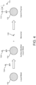
- thermal interface material 48 ( FIG. 1 ) is comprised of liquid metal 102 and a polymer 112 including a monomer 104 and a monomer 108.
- the liquid metal 102 is blended with monomer 104 to form surface modified liquid metal, which upon polymerization with monomer 108 led to the polymer 112 to form the thermal interface material 114 (e.g., a copolymerized material) in some embodiments.
- the liquid metal 102 is liquid at room temperature and is encapsulated inside of the polymer 112.
- the characteristics (e.g., thermal expansion, etc.) of the liquid metal 102 and polymer 112 are chosen to be compatible for stability across environmental conditions.
- thermal interface material 48 includes polymer 112 (e.g., an elastomer matrix) embedded with liquid metal 102.
- the liquid metal 102 has a spherical shape (e.g., micro droplets) due to lowest surface energy for a given volume.
- the monomer 104 bonds to the liquid metal 102 and modifies the surface of the liquid metal 102.
- organometallic chemistry uses a catalyst to attach monomer 104 directly to the liquid metal 102.
- the surface of the spherical liquid metal material is modified such that the spheres become elongated. Ultraviolet light, heat, and other activating techniques can be utilized. A metal bond or an organometallic bond is formed which is robust in some embodiments.
- Monomer 104 includes an R group (e.g., R 1 group) and an X and/or Y group in some embodiments. R groups and X and Y groups are discussed below. The bond between liquid metal 102 and monomer 104 is formed using the X and/or Y group in some embodiments.
- Monomer 108 includes silicon in some embodiments.
- Monomer 104 also includes silicon in some embodiments.
- Monomer 108 includes an R group (e.g., R 2 group).
- the monomer 108 overcomes limitations associated with limitations of liquid metal polymers.
- Polymer 112 includes R1 bonded to R2 with m X portions and n R 2 portions (e.g., R-(-R)n) where m and n are integers (e.g., 100 -100000 ) in some embodiments. Polymer 112 combined with liquid metal 102 forms polymeric matrix 114 in some embodiments.
- thermal interface material 48 ( FIG. 1 ) is comprised of liquid metal 102 and a polymer 204 including at least two R groups (e.g., monomers) and a Z group. R groups and X and Y groups are discussed below. The bond between liquid metal 102 and polymer 204 is formed using the Z group in some embodiments.
- the liquid metal 102 is blended with the polymer 204 to form the thermal interface material 48 as hybrid polymeric matrix 212.
- Polymer 204 includes an R group bonded to another R group with a Z group and n + 1 R portions (e.g., R-( ⁇ -R)n) where m is an integer (e.g.,100-100000 ).
- Polymeric matrix 212 is similar to polymeric matrix 114 in some embodiments.
- the bond between liquid metal 102 and polymer 204 is formed using the Z group in some embodiments.
- a table 250 includes a first column showing exemplary X, Y, and Z groups, a second column showing exemplary R 1 groups with X, Y and Z group locations, a third column showing exemplary R-(-R)n groups with X, Y and Z group locations, and a fourth column showing exemplary R 2 groups with X, Y and Z group locations.
- the first three rows (rows A-C) list X or Y groups.
- the NH location provides additional bonding in some embodiments.
- the symbol ⁇ represents the bond location to R 1 or R 2 groups.
- Row B shows non-silicon based groups for R 1 and R 2 groups.
- the third row (row C) of table 250 shows a single R 1 group without an R 2 group and the R 1 group of Row C is bondable to the Z group in the fourth row (row D).
- the R 1 and R 2 groups in row D are bondable to X and Y groups.
- a table 280 lists exemplary combinations of the R 1 and R 2 groups and X, Y, and Z groups provided in FIG. 7 , where each row is a unique combination.
- polymer 1a is a combination of the R 1 and R 2 groups and X and Y groups from row A of table 250.
- Polymer 1b is a combination of the R 1 and R 2 groups and the X group from row A of table 250 and the Y group from row B of table 250.
- Polymer 1c is a combination of the R 1 and R 2 groups and the X group from row A of table 250 and the Y group from row c of table 250.
- Polymer 3 is a combination of the R 1 group from row A of table 250 and the Z group from row D of table 250.
- Polymer 4a is a combination of the R 1 and R 2 groups from row D of table 250 and the X and Y group from row A of table 250.
- Other combinations are indicated in table 250 according to similar conventions.
- the symbol N/A refers to the term not applicable. Additional combinations of monomers are possible.
- first and second in connection with devices for purposes of identifying or differentiating one from another or from others. These terms are not intended to relate entities or operations (e.g., a first region and a second region) temporally or according to a sequence, although in some cases, these entities can include such a relationship. Nor do these terms limit the number of possible entities or operations.
- circuits described above can provide multiple ones of any or each of those components.
- the structures, circuits and methods described above can be adjusted for various system parameters and design criteria, such as shape, depth, thicknesses, material, etc.
- direct coupling is not shown in a limiting fashion and is exemplarily shown.
- Alternative embodiments include circuits with indirect coupling or indirect attachment between the components shown.
Landscapes
- Chemical & Material Sciences (AREA)
- Engineering & Computer Science (AREA)
- Materials Engineering (AREA)
- Physics & Mathematics (AREA)
- Chemical Kinetics & Catalysis (AREA)
- Combustion & Propulsion (AREA)
- Thermal Sciences (AREA)
- Organic Chemistry (AREA)
- Structures Or Materials For Encapsulating Or Coating Semiconductor Devices Or Solid State Devices (AREA)
Abstract
Description
- One or more integrated circuits (ICs) can be provided on or within a module or integrated circuit package. The package can be a multi-chip module or a single chip package. Each of the one or more ICs is generally provided on a die that is connected by fine wires or by solder bumps to a package substrate. The single chip package or multichip module often includes a cover or other protective structure that covers the one or more ICs. The term integrated circuit or IC package as used herein includes single chip packages and multi-chip modules.
- According to an aspect of the invention, a package is provided, comprising:
- a one or more die;
- a package substrate;
- a thermal interface material; and
- a cover disposed over the one or more die, wherein the thermal interface material comprises modified liquid metal material and a first monomer comprising silicon.
- Advantageously, the one or more die are attached to the package substrate.
- Advantageously, the one or more die are attached to the package substrate by solder balls.
- Advantageously, the one or more die are attached using a flip chip configuration.
- Advantageously, the thermal interface material is disposed between the cover and the one or more die.
- Advantageously, the thermal interface material is comprised of a polymer comprising the first monomer and wherein the polymer is bonded to the liquid metal by an organometallic bond, coordinate, or a covalent bond.
- Advantageously, the cover is attached to the package substrate and the one or more die are attached to the package substrate.
- Advantageously, the thermal interface material is comprised of surface modified liquid spheres.
- Advantageously, the thermal interface material is comprised of a polymer comprised of the first monomer and a second monomer.
- Advantageously, the second monomer is bonded to the first monomer.
- According to an aspect, a method is provided of fabricating an integrated circuit package, the method comprising:
- attaching a die to a substrate;
- providing a polymerized material comprising two monomers and a liquid metal, the liquid metal being bonded by a covalent bond or organometallic bond to at least one of the two monomers; and
- providing a cover over the die, wherein the polymerized material is disposed in at least a region between the cover and the die.
- Advantageously, the polymerized material is a polymer matrix and at least one of the monomers comprises a silicon monomer.
- Advantageously, the liquid metal is liquid at room temperature.
- Advantageously, the liquid metal is shaped in spheres.
- Advantageously, the polymerized material is a polymer matrix and the spheres are evenly distributed in the polymer matrix.
- According to an aspect, a thermal interface material for an integrated circuit package is provided, the thermal interface material comprising:
a polymer matrix comprising copolymerized modified liquid-metal and a monomer attached to the liquid metal using C = O, S = O, N:, NH, and/or OH moiety. - Advantageously, the polymeric matrix comprises two or more monomers.
- Advantageously, the modified liquid-metal in the polymeric matrix comprises surface modified liquid metal spheres.
- Advantageously, the surface modified liquid metal spheres are evenly distributed in the polymer matrix.
- Advantageously, the monomer comprises silicon and is an adhesion promoter.
- Various objects, aspects, features, and advantages of the disclosure will become more apparent and better understood by referring to the detailed description taken in conjunction with the accompanying drawings, in which like reference characters identify corresponding elements throughout. In the drawings, like reference numbers generally indicate identical, functionally similar, and/or structurally similar elements.
-
FIG. 1 is a cross sectional view schematic drawing of an integrated circuit package according to some embodiments; -
FIG. 2 is a more detailed cross sectional view schematic drawing of the integrated circuit package illustrated inFIG. 1 showing a cover, an integrated circuit (IC) die and a thermal interface material (TIM), according to some embodiments; -
FIG. 3 is flow diagram showing exemplary operations for fabricating the integrated circuit package illustrated inFIG. 1 according to some embodiments; -
FIG. 4 is a flow diagram showing exemplary operations for fabricating a polymerized liquid metal matrix for the integrated circuit package illustrated inFIG. 1 according to some embodiments; -
FIG. 5 is a flow diagram showing exemplary operations for fabricating a polymerized liquid metal matrix for the integrated circuit package illustrated inFIG. 1 according to some embodiments; -
FIG. 6 is a diagram showing exemplary monomers for use in the exemplary operations illustrated inFIGS. 4-5 according to some embodiments; and -
FIG. 7 is a diagram showing exemplary combinations of the monomers shown inFIG. 7 according to some embodiments. - Before turning to the features, which illustrate some exemplary embodiments in detail, it should be understood that the application is not limited to the details or methodology set forth in the description or illustrated in the Figures. It should also be understood that the terminology is for the purpose of description only and should not be regarded as limiting.
- Referring generally to the Figures, devices can be provided in IC packages (e.g., as single chip packages having a single IC or as a system in package (SiP) having two or more ICs or dies in a package (e.g., a multi-chip module) according to various exemplary embodiments. IC packages and methods related to IC packages utilize surface modified liquid metal spheres to provide a robust liquid metal polymer composite thermal interface material in some embodiments. In some embodiments, a liquid metal polymer composite thermal interface material provides superior heat extraction. The liquid metal polymer composite thermal interface material provides a more heat conductive path to a heat sink or heat spreader in some embodiments. In some embodiments, the thermal interface material is configured to be thermally and mechanically reliable and can be used in higher power IC devices. In some embodiments, copolymerization of surface modified liquid-metal and silicon monomers provides a robust material with uniform distribution of thermally conductive liquid-metal in the polymer matrix.
- Liquid metal has high thermal conductivity but generally exhibits poor reliability. Liquid metal loaded polymers have good thermal conductivity and reliability but generally lack homogeneity - liquid metal is severely depleted at the edges due to insufficient interaction between liquid metal and polymer. Silicon monomers organo-metallically or covalently bonded to the liquid metal create copolymerized silicon monomers that provide strong bonding and overcome the limitations of certain conventional liquid metal loaded polymers in some embodiments.
- According to some embodiments, a package includes a one or more die, a package substrate, a thermal interface material, and a cover. The cover is disposed over or above the one or more die. The thermal interface material includes a surface modified metal and a silicon monomer.
- Some embodiments relate to a method of fabricating an integrated circuit package. The method includes attaching a die to a substrate, providing a polymerized material including two monomers and a liquid metal. The liquid metal is bonded by a covalent bond or organometallic bond to at least one of the two monomers. The method also includes providing a cover over the die, and the polymerized material is disposed in at least a region between the cover and the die.
- Some embodiments relate to a thermal interface material for an integrated circuit package. The thermal interface material includes a polymer matrix comprising copolymerized modified liquid-metal and a silicon monomer.
- Some embodiments relate to a thermal interface material for an integrated circuit package. The thermal interface material includes a polymer matrix comprising copolymerized modified liquid-metal and a monomer attached to the liquid metal using at an: C = O, S = O, N:, NH, and/or OH moiety.
- With reference to
FIG. 1 , an integrated circuit package 10 (e.g., system in package (SiP)) includes cover 12 (e.g., a lid), apackage substrate 14, aninterconnect board 16, adie 30, adie 32, adie 34, andthermal interface material 48. Integratedcircuit package 10 is a single die package or a multiple die package in some embodiments. Integratedcircuit package 10 is configured for side-by-side die packaging, three dimensional packaging, embedded packaging, and other configurations for containing one or more ofdie circuit package 10 and components thereof can have a variety thicknesses and sizes depending on die area and system criteria. - A set 28 of solder balls can interconnect
board 16 to die 30, 32, and 34 in some embodiments. Thedie interconnect board 16 in a flip chip configuration in some embodiments. Theset 28 of solder balls can be pins, solder bumps, wires, or other structures for coupling die 30, 32, and 34 to interconnectboard 16 or other circuit boards, other devices, or substrates in some embodiments. In some embodiments, die 30, 32, and 34 are coupled directly to thepackage substrate 14 by solder balls, pins, solder bump, wires, or other structures. -
Die Die substrate 14 viaset 28 of solder balls andinterconnect board 16 in some embodiments. A set 18 of solder balls can be provided on a bottom ofsubstrate 14 for coupling to circuit boards or other components. The set 18 of solder balls can be pins, solder bump, wires, or other structures. - The
substrate 14 andinterconnect board 16 can be any type of IC package circuit board. In some embodiments,interconnect board 16 andpackage substrate 14 are ceramic boards. In some embodiments,interconnect board 16 andpackage substrate 14 are alumina, aluminum nitride or beryllium oxide, flex, or fiberglass circuit boards. -
Cover 12 is a metal, metal composite, or ceramic material in some embodiments.Cover 12 is adhered tosubstrate 14 in some embodiments.Cover 12 can be coupled to or integrated with a heat sink or heat spreader for heat dissipation in some embodiments.Cover 12 is tungsten, copper, copper-diamond, silver-diamond, aluminum, silicon carbide, gold, nickel, and alloys thereof in some embodiments. - With reference to
FIGS. 1 and2 ,thermal interface material 48 is disposed in a region betweencover 12 and at least one ofdie enlarged area 62 of integratedcircuit package 10 is shown inFIG. 2 .Thermal interface material 48 can be provided in other regions where thermal conductivity is desired. In some embodiments,thermal interface material 48 is configured for heat dissipation and is an insulating material. In some embodiments,thermal interface material 48 includes a liquid metal material disposed in a polymerized matrix. The liquid metal material is liquid phase eutectic gallium-indium micro droplets in some embodiments. In some embodiments,thermal interface material 48 is configured for homogeneity in the polymerized matrix and is not significantly depleted at edges of the polymerized matrix.Arrows 1 and 2 show heat dissipation through thedie 32 and thethermal interface material 48 to the cover orcover 12. - With reference to
FIG. 3 , aflow 200 is performed to fabricate theintegrated circuit package 10 with thethermal interface material 48. Flow 200 exemplary only and is not limited to operations performed in a particular order. - At an
operation 202, one or more die (e.g., die 30, 32, and 34) are attached to interconnectboard 16 or other circuit board/substrate for housing die. The interconnect board16 can be a single package substrate which is part of theintegrated circuit package 10 or can be one of two or more circuit boards in theintegrated circuit package 10. The interconnect board16 is an intermediate board, interposer, or the top most or bottom most substrate (e.g., package substrate 14) in some embodiments.Die die interconnect board 16 include adhesives, wire bonding, and pins. - At an
operation 203, a polymerized matrix including liquid metal material is provided. The polymerized matrix is provided over or above die 32, 34, and/or 36 as the thermal interface material 48 (FIG. 1 ) betweendie 32 and cover 12 in some embodiments. The polymerized matrix is dispensed, deposited, spin-coated, injected, sprayed, spread, applied as a pre-formed film, or otherwise applied above thepackage substrate 16 and die 30, 32, and/or 34 in some embodiments. The polymerized matrix includes silicon in some embodiments. In some embodiments, the polymerized matrix includes two monomers with one monomer bonded to the liquid metal material and the other monomer bonded to the monomer bonded to the liquid metal material. In some embodiments, the polymerized matrix is formed as described below with reference toFIGS. 4-7 . - In some embodiments, the materials such as polysiloxane (e.g. silicone, polydimethylsiloxane, RTV silicones), polyurethane, polyacrylate, natural (latex) rubber, polyisobutylene, block copolymer elastomers (e.g. styrene ethylene butylene styrene), polychloroprene, thermoplastic elastomers ( e.g. propylene-ethylene co-polymer), polyphenylenes and their derivatives, polybutadiene, butadiene-acrylonitrile, vinyl acetates, polyurethanes, polyamides, and other similar materials can be included in the polymerized matrix. In some embodiments, the liquid metal material is included in the polymerized matrix and includes materials, such as, eutectic gallium indium (EGain), gallium-indium-tin (Galinstan), Indalloy, NewMerc, mercury, other metals that are liquid at lower temperatures than other metals, and combinations and alloys thereof.
- In an
operation 206, acover 12 is provided overdie substrate 14 orinterconnect board 16.Operation 206 can be performed before or afteroperation 203.Cover 12 is adhered to packagesubstrate 14 about its perimeter in some embodiments.Cover 12 can be soldered or otherwise connected to packagesubstrate 14 orinterconnect board 16 in some embodiments. - With reference to
FIG. 4 , thermal interface material 48 (FIG. 1 ) is comprised ofliquid metal 102 and apolymer 112 including amonomer 104 and amonomer 108. Theliquid metal 102 is blended withmonomer 104 to form surface modified liquid metal, which upon polymerization withmonomer 108 led to thepolymer 112 to form the thermal interface material 114 (e.g., a copolymerized material) in some embodiments. Theliquid metal 102 is liquid at room temperature and is encapsulated inside of thepolymer 112. In some embodiments, the characteristics (e.g., thermal expansion, etc.) of theliquid metal 102 andpolymer 112 are chosen to be compatible for stability across environmental conditions. In some embodiments,thermal interface material 48 includes polymer 112 (e.g., an elastomer matrix) embedded withliquid metal 102. - In some embodiments, the
liquid metal 102 has a spherical shape (e.g., micro droplets) due to lowest surface energy for a given volume. Themonomer 104 bonds to theliquid metal 102 and modifies the surface of theliquid metal 102. In some embodiments, organometallic chemistry uses a catalyst to attachmonomer 104 directly to theliquid metal 102. In some embodiments, the surface of the spherical liquid metal material is modified such that the spheres become elongated. Ultraviolet light, heat, and other activating techniques can be utilized. A metal bond or an organometallic bond is formed which is robust in some embodiments. -
Monomer 104 includes an R group (e.g., R1 group) and an X and/or Y group in some embodiments. R groups and X and Y groups are discussed below. The bond betweenliquid metal 102 andmonomer 104 is formed using the X and/or Y group in some embodiments. - After the
monomer 104 is bonded toliquid metal 102, amonomer 108 is added.Monomer 108 includes silicon in some embodiments.Monomer 104 also includes silicon in some embodiments.Monomer 108 includes an R group (e.g., R2 group).Monomer 108 bonds to monomer 104 (e.g., R1 group is covalently bonded to R2 group) to form apolymer 112 in some embodiments. In some embodiments, themonomer 108 overcomes limitations associated with limitations of liquid metal polymers.Polymer 112 includes R1 bonded to R2 with m X portions and n R2 portions (e.g., R-(-R)n) where m and n are integers (e.g., 100 -100000 ) in some embodiments.Polymer 112 combined withliquid metal 102 formspolymeric matrix 114 in some embodiments. - With reference to
FIG. 5 , thermal interface material 48 (FIG. 1 ) is comprised ofliquid metal 102 and apolymer 204 including at least two R groups (e.g., monomers) and a Z group. R groups and X and Y groups are discussed below. The bond betweenliquid metal 102 andpolymer 204 is formed using the Z group in some embodiments. - The
liquid metal 102 is blended with thepolymer 204 to form thethermal interface material 48 as hybridpolymeric matrix 212.Polymer 204 includes an R group bonded to another R group with a Z group and n + 1 R portions (e.g., R-(̵-R)n) where m is an integer (e.g.,100-100000 ).Polymeric matrix 212 is similar topolymeric matrix 114 in some embodiments. The bond betweenliquid metal 102 andpolymer 204 is formed using the Z group in some embodiments. - With reference to
FIG. 6 , a table 250 includes a first column showing exemplary X, Y, and Z groups, a second column showing exemplary R1 groups with X, Y and Z group locations, a third column showing exemplary R-(-R)n groups with X, Y and Z group locations, and a fourth column showing exemplary R2 groups with X, Y and Z group locations. In the first column of table 250, the first three rows (rows A-C) list X or Y groups. The X or Y groups bond to the liquid metal 102 (FIG. 4 ) at the C=O/OH location in some embodiments. The NH location provides additional bonding in some embodiments. The symbol {represents the bond location to R1 or R2 groups. Row B shows non-silicon based groups for R1 and R2 groups. - The third row (row C) of table 250 shows a single R1 group without an R2 group and the R1 group of Row C is bondable to the Z group in the fourth row (row D). The R1 and R2 groups in row D are bondable to X and Y groups.
- With reference to FIG. 8, a table 280 lists exemplary combinations of the R1 and R2 groups and X, Y, and Z groups provided in
FIG. 7 , where each row is a unique combination. Nineteen exemplary combinations are shown inFIG. 7 . For example, polymer 1a is a combination of the R1 and R2 groups and X and Y groups from row A of table 250.Polymer 1b is a combination of the R1 and R2 groups and the X group from row A of table 250 and the Y group from row B of table 250.Polymer 1c is a combination of the R1 and R2 groups and the X group from row A of table 250 and the Y group from row c of table 250.Polymer 3 is a combination of the R1 group from row A of table 250 and the Z group from row D of table 250.Polymer 4a is a combination of the R1 and R2 groups from row D of table 250 and the X and Y group from row A of table 250. Other combinations are indicated in table 250 according to similar conventions. The symbol N/A refers to the term not applicable. Additional combinations of monomers are possible. - The dimensions, thicknesses, configurations and materials disclosed herein are exemplary only. Although only a side-by-side multichip configuration is shown, additional layers and configurations including dies can be added (e.g., three die stack configuration or more) in some embodiments.
- The disclosure is described above with reference to drawings. These drawings illustrate certain details of specific embodiments that implement the systems and methods and programs of the present disclosure. However, describing the disclosure with drawings should not be construed as imposing on the disclosure any limitations that are present in the drawings. The embodiments of the present disclosure can be implemented using various types of dies. No claim element herein is to be construed as a "means plus function" element unless the element is expressly recited using the phrase "means for." Furthermore, no element, component or method step in the present disclosure is intended to be dedicated to the public, regardless of whether the element, component or method step is explicitly recited in the claims.
- It should be noted that certain passages of this disclosure can reference terms such as "first" and "second" in connection with devices for purposes of identifying or differentiating one from another or from others. These terms are not intended to relate entities or operations (e.g., a first region and a second region) temporally or according to a sequence, although in some cases, these entities can include such a relationship. Nor do these terms limit the number of possible entities or operations.
- It should be understood that the circuits described above can provide multiple ones of any or each of those components. In addition, the structures, circuits and methods described above can be adjusted for various system parameters and design criteria, such as shape, depth, thicknesses, material, etc. Although shown in the drawings with certain components directly coupled to each other, direct coupling is not shown in a limiting fashion and is exemplarily shown. Alternative embodiments include circuits with indirect coupling or indirect attachment between the components shown.
- It should be noted that although steps are described in an order, it is understood that the order of these steps can differ from what is depicted. Also two or more steps can be performed concurrently or with partial concurrence. Such variation will depend on the recipes and systems chosen and on designer choice. It is understood that all such variations are within the scope of the disclosure.
- While the foregoing written description of the methods and systems enables one of ordinary skill to make and use what is considered presently to be the best-mode thereof, those of ordinary skill will understand and appreciate the existence of variations, combinations, and equivalents of the specific embodiment, method, and examples herein. The present methods and systems should therefore not be limited by the above described embodiments, methods, and examples, but by all embodiments and methods within the scope and spirit of the disclosure.
Claims (15)
- A package, comprising:a one or more die;a package substrate;a thermal interface material; anda cover disposed over the one or more die, wherein the thermal interface material comprises modified liquid metal material and a first monomer comprising silicon.
- The package of claim 1, wherein the one or more die are attached to the package substrate.
- The package of claim 1, wherein the one or more die are attached to the package substrate by solder balls.
- The package of claim 1, wherein the one or more die are attached using a flip chip configuration.
- The package of claim 1, wherein the thermal interface material is disposed between the cover and the one or more die.
- The package of claim 1, wherein the thermal interface material is comprised of a polymer comprising the first monomer and wherein the polymer is bonded to the liquid metal by an organometallic bond, coordinate, or a covalent bond.
- The package of claim 6, wherein the cover is attached to the package substrate and the one or more die are attached to the package substrate.
- The package of claim 1, wherein the thermal interface material is comprised of surface modified liquid spheres.
- The package of claim 1, the thermal interface material is comprised of a polymer comprised of the first monomer and a second monomer.
- The package of claim 9, wherein the second monomer is bonded to the first monomer.
- A method of fabricating an integrated circuit package, the method comprising:attaching a die to a substrate;providing a polymerized material comprising two monomers and a liquid metal, the liquid metal being bonded by a covalent bond or organometallic bond to at least one of the two monomers; andproviding a cover over the die, wherein the polymerized material is disposed in at least a region between the cover and the die.
- The method of claim 11, wherein the polymerized material is a polymer matrix and at least one of the monomers comprises a silicon monomer.
- The method of claim 12, wherein the liquid metal is liquid at room temperature.
- The method of claim 11, wherein the liquid metal is shaped in spheres.
- A thermal interface material for an integrated circuit package, the thermal interface material comprising:
a polymer matrix comprising copolymerized modified liquid-metal and a monomer attached to the liquid metal using C = O, S = O, N:, NH, and/or OH moiety.
Priority Applications (2)
| Application Number | Priority Date | Filing Date | Title |
|---|---|---|---|
| EP23196773.8A EP4283669A3 (en) | 2021-07-30 | 2022-07-20 | Integrated circuit package with surface modified liquid metal spheres and method of making |
| EP23196769.6A EP4283668A3 (en) | 2021-07-30 | 2022-07-20 | Integrated circuit package with surface modified liquid metal spheres and method of making |
Applications Claiming Priority (1)
| Application Number | Priority Date | Filing Date | Title |
|---|---|---|---|
| US17/390,474 US12438062B2 (en) | 2021-07-30 | 2021-07-30 | Polymerized thermal interface material with surface modified liquid metal spheres and method of making |
Related Child Applications (2)
| Application Number | Title | Priority Date | Filing Date |
|---|---|---|---|
| EP23196769.6A Division EP4283668A3 (en) | 2021-07-30 | 2022-07-20 | Integrated circuit package with surface modified liquid metal spheres and method of making |
| EP23196773.8A Division EP4283669A3 (en) | 2021-07-30 | 2022-07-20 | Integrated circuit package with surface modified liquid metal spheres and method of making |
Publications (1)
| Publication Number | Publication Date |
|---|---|
| EP4124641A1 true EP4124641A1 (en) | 2023-02-01 |
Family
ID=82656722
Family Applications (3)
| Application Number | Title | Priority Date | Filing Date |
|---|---|---|---|
| EP22186026.5A Pending EP4124641A1 (en) | 2021-07-30 | 2022-07-20 | Integrated circuit package with surface modified liquid metal spheres and method of making |
| EP23196773.8A Pending EP4283669A3 (en) | 2021-07-30 | 2022-07-20 | Integrated circuit package with surface modified liquid metal spheres and method of making |
| EP23196769.6A Pending EP4283668A3 (en) | 2021-07-30 | 2022-07-20 | Integrated circuit package with surface modified liquid metal spheres and method of making |
Family Applications After (2)
| Application Number | Title | Priority Date | Filing Date |
|---|---|---|---|
| EP23196773.8A Pending EP4283669A3 (en) | 2021-07-30 | 2022-07-20 | Integrated circuit package with surface modified liquid metal spheres and method of making |
| EP23196769.6A Pending EP4283668A3 (en) | 2021-07-30 | 2022-07-20 | Integrated circuit package with surface modified liquid metal spheres and method of making |
Country Status (3)
| Country | Link |
|---|---|
| US (1) | US12438062B2 (en) |
| EP (3) | EP4124641A1 (en) |
| CN (1) | CN115692328A (en) |
Families Citing this family (3)
| Publication number | Priority date | Publication date | Assignee | Title |
|---|---|---|---|---|
| US20230418009A1 (en) * | 2022-06-26 | 2023-12-28 | International Business Machines Corporation | Thermal management of computer hardware modules |
| US12027442B1 (en) | 2023-01-31 | 2024-07-02 | Arieca Inc. | Thermal interface material, an integrated circuit formed therewith, and a method of application thereof |
| WO2024186969A1 (en) * | 2023-03-08 | 2024-09-12 | Arieca Inc. | Thermal interface materials comprising functionalized liquid metal droplets, circuit assemblies formed therefrom, and methods of manufacture thereof |
Citations (3)
| Publication number | Priority date | Publication date | Assignee | Title |
|---|---|---|---|---|
| US20040262740A1 (en) * | 2003-06-30 | 2004-12-30 | Matayabas James C. | Polymer solder hybrid interface material with improved solder filler particle size and microelectronic package application |
| US20050228097A1 (en) * | 2004-03-30 | 2005-10-13 | General Electric Company | Thermally conductive compositions and methods of making thereof |
| US20180323130A1 (en) * | 2015-12-22 | 2018-11-08 | Intel Corporation | Adhesive polymer thermal interface material with sintered fillers for thermal conductivity in micro-electronic packaging |
Family Cites Families (10)
| Publication number | Priority date | Publication date | Assignee | Title |
|---|---|---|---|---|
| JP5103364B2 (en) * | 2008-11-17 | 2012-12-19 | 日東電工株式会社 | Manufacturing method of heat conductive sheet |
| KR101532026B1 (en) * | 2014-06-03 | 2015-06-29 | 지앤씨테크(주) | Heat releasing composite and manufacturing method for the same |
| US9937662B2 (en) * | 2016-09-01 | 2018-04-10 | International Business Machines Corporation | Shape memory thermal interface materials |
| US10937716B2 (en) * | 2017-12-12 | 2021-03-02 | Arizona Board Of Regents On Behalf Of Arizona State University | Multi-layer thin film composite thermal interface materials |
| US10777483B1 (en) * | 2020-02-28 | 2020-09-15 | Arieca Inc. | Method, apparatus, and assembly for thermally connecting layers |
| KR102356658B1 (en) * | 2020-03-31 | 2022-01-26 | 포항공과대학교 산학협력단 | Stretchable electrode circuit having three-dimensional circuit printing ability, strain sensor using same and method of fabricating same |
| US12486443B2 (en) * | 2020-09-25 | 2025-12-02 | Carnegie Mellon University | Multifunctional shape morphing elastomer with liquid metal inclusions |
| US20220199489A1 (en) * | 2020-12-23 | 2022-06-23 | Intel Corporation | Gallium alloys as fillers for polymer thermal interface materials |
| US11699631B2 (en) * | 2021-02-24 | 2023-07-11 | Taiwan Semiconductor Manufacturing Company, Ltd. | Semiconductor device and manufacturing method thereof |
| US20240174816A1 (en) * | 2021-05-03 | 2024-05-30 | Nanyang Technological University | Flexible effective heat transport composites for thermal interface applications |
-
2021
- 2021-07-30 US US17/390,474 patent/US12438062B2/en active Active
-
2022
- 2022-07-08 CN CN202210804965.0A patent/CN115692328A/en active Pending
- 2022-07-20 EP EP22186026.5A patent/EP4124641A1/en active Pending
- 2022-07-20 EP EP23196773.8A patent/EP4283669A3/en active Pending
- 2022-07-20 EP EP23196769.6A patent/EP4283668A3/en active Pending
Patent Citations (3)
| Publication number | Priority date | Publication date | Assignee | Title |
|---|---|---|---|---|
| US20040262740A1 (en) * | 2003-06-30 | 2004-12-30 | Matayabas James C. | Polymer solder hybrid interface material with improved solder filler particle size and microelectronic package application |
| US20050228097A1 (en) * | 2004-03-30 | 2005-10-13 | General Electric Company | Thermally conductive compositions and methods of making thereof |
| US20180323130A1 (en) * | 2015-12-22 | 2018-11-08 | Intel Corporation | Adhesive polymer thermal interface material with sintered fillers for thermal conductivity in micro-electronic packaging |
Also Published As
| Publication number | Publication date |
|---|---|
| US20230034217A1 (en) | 2023-02-02 |
| EP4283668A2 (en) | 2023-11-29 |
| EP4283669A3 (en) | 2024-02-28 |
| EP4283669A2 (en) | 2023-11-29 |
| US12438062B2 (en) | 2025-10-07 |
| CN115692328A (en) | 2023-02-03 |
| EP4283668A3 (en) | 2024-02-28 |
Similar Documents
| Publication | Publication Date | Title |
|---|---|---|
| EP4283669A2 (en) | Integrated circuit package with surface modified liquid metal spheres and method of making | |
| US12381119B2 (en) | Seal for microelectronic assembly | |
| US11133237B2 (en) | Package with embedded heat dissipation features | |
| US8526186B2 (en) | Electronic assembly including die on substrate with heat spreader having an open window on the die | |
| US5552635A (en) | High thermal emissive semiconductor device package | |
| KR100269528B1 (en) | High performance, low cost multi-chip module package | |
| US12033912B2 (en) | Package structure and manufacturing method thereof | |
| EP2259309A2 (en) | Integrated circuit package including a thermally and electrically conductive package lid | |
| US9812374B1 (en) | Thermal management device with textured surface for extended cooling limit | |
| WO2007117931A2 (en) | Controlling flip-chip techniques for concurrent ball bonds in semiconductor devices | |
| TWI741388B (en) | Semiconductor package and manufacturing method thereof | |
| CN112447638A (en) | Semiconductor package | |
| CN115249674A (en) | Packaging assembly | |
| CN114975138A (en) | Package structure and method for forming the same | |
| US11869822B2 (en) | Semiconductor package and manufacturing method thereof | |
| TW200901396A (en) | Semiconductor device package having chips | |
| CN114628337A (en) | Semiconductor device and method for manufacturing the same | |
| US6965163B2 (en) | Substrate-less microelectronic package | |
| CN112802764B (en) | Package and method of forming the same | |
| WO2022124895A2 (en) | Integrated circuit comprising improved die attachment layer | |
| JP3372498B2 (en) | Semiconductor device | |
| Bu et al. | Thermal design and analysis of through silicon interposer (TSI) package |
Legal Events
| Date | Code | Title | Description |
|---|---|---|---|
| PUAI | Public reference made under article 153(3) epc to a published international application that has entered the european phase |
Free format text: ORIGINAL CODE: 0009012 |
|
| STAA | Information on the status of an ep patent application or granted ep patent |
Free format text: STATUS: THE APPLICATION HAS BEEN PUBLISHED |
|
| AK | Designated contracting states |
Kind code of ref document: A1 Designated state(s): AL AT BE BG CH CY CZ DE DK EE ES FI FR GB GR HR HU IE IS IT LI LT LU LV MC MK MT NL NO PL PT RO RS SE SI SK SM TR |
|
| STAA | Information on the status of an ep patent application or granted ep patent |
Free format text: STATUS: REQUEST FOR EXAMINATION WAS MADE |
|
| 17P | Request for examination filed |
Effective date: 20230801 |
|
| RBV | Designated contracting states (corrected) |
Designated state(s): AL AT BE BG CH CY CZ DE DK EE ES FI FR GB GR HR HU IE IS IT LI LT LU LV MC MK MT NL NO PL PT RO RS SE SI SK SM TR |
|
| STAA | Information on the status of an ep patent application or granted ep patent |
Free format text: STATUS: EXAMINATION IS IN PROGRESS |
|
| 17Q | First examination report despatched |
Effective date: 20250901 |
|
| GRAP | Despatch of communication of intention to grant a patent |
Free format text: ORIGINAL CODE: EPIDOSNIGR1 |
|
| STAA | Information on the status of an ep patent application or granted ep patent |
Free format text: STATUS: GRANT OF PATENT IS INTENDED |
|
| RIC1 | Information provided on ipc code assigned before grant |
Ipc: C09K 5/14 20060101AFI20260116BHEP Ipc: H10W 40/25 20260101ALI20260116BHEP |
|
| INTG | Intention to grant announced |
Effective date: 20260130 |