EP4120333A1 - Preparation method for semiconductor structure - Google Patents
Preparation method for semiconductor structure Download PDFInfo
- Publication number
- EP4120333A1 EP4120333A1 EP21935429.7A EP21935429A EP4120333A1 EP 4120333 A1 EP4120333 A1 EP 4120333A1 EP 21935429 A EP21935429 A EP 21935429A EP 4120333 A1 EP4120333 A1 EP 4120333A1
- Authority
- EP
- European Patent Office
- Prior art keywords
- region
- layer
- transistor
- oxide layer
- manufacturing
- Prior art date
- Legal status (The legal status is an assumption and is not a legal conclusion. Google has not performed a legal analysis and makes no representation as to the accuracy of the status listed.)
- Withdrawn
Links
Images


Classifications
-
- H—ELECTRICITY
- H10—SEMICONDUCTOR DEVICES; ELECTRIC SOLID-STATE DEVICES NOT OTHERWISE PROVIDED FOR
- H10B—ELECTRONIC MEMORY DEVICES
- H10B12/00—Dynamic random access memory [DRAM] devices
- H10B12/01—Manufacture or treatment
- H10B12/02—Manufacture or treatment for one transistor one-capacitor [1T-1C] memory cells
- H10B12/05—Making the transistor
-
- H—ELECTRICITY
- H10—SEMICONDUCTOR DEVICES; ELECTRIC SOLID-STATE DEVICES NOT OTHERWISE PROVIDED FOR
- H10B—ELECTRONIC MEMORY DEVICES
- H10B12/00—Dynamic random access memory [DRAM] devices
- H10B12/01—Manufacture or treatment
- H10B12/09—Manufacture or treatment with simultaneous manufacture of the peripheral circuit region and memory cells
-
- H—ELECTRICITY
- H10—SEMICONDUCTOR DEVICES; ELECTRIC SOLID-STATE DEVICES NOT OTHERWISE PROVIDED FOR
- H10B—ELECTRONIC MEMORY DEVICES
- H10B12/00—Dynamic random access memory [DRAM] devices
- H10B12/50—Peripheral circuit region structures
-
- H—ELECTRICITY
- H10—SEMICONDUCTOR DEVICES; ELECTRIC SOLID-STATE DEVICES NOT OTHERWISE PROVIDED FOR
- H10D—INORGANIC ELECTRIC SEMICONDUCTOR DEVICES
- H10D64/00—Electrodes of devices having potential barriers
- H10D64/01—Manufacture or treatment
- H10D64/013—Manufacture or treatment of electrodes having a conductor capacitively coupled to a semiconductor by an insulator
- H10D64/01302—Manufacture or treatment of electrodes having a conductor capacitively coupled to a semiconductor by an insulator the insulator being formed after the semiconductor body, the semiconductor being silicon
- H10D64/01332—Making the insulator
- H10D64/01352—Making the insulator with sacrificial oxide
-
- H—ELECTRICITY
- H10—SEMICONDUCTOR DEVICES; ELECTRIC SOLID-STATE DEVICES NOT OTHERWISE PROVIDED FOR
- H10D—INORGANIC ELECTRIC SEMICONDUCTOR DEVICES
- H10D64/00—Electrodes of devices having potential barriers
- H10D64/60—Electrodes characterised by their materials
- H10D64/66—Electrodes having a conductor capacitively coupled to a semiconductor by an insulator, e.g. MIS electrodes
- H10D64/68—Electrodes having a conductor capacitively coupled to a semiconductor by an insulator, e.g. MIS electrodes characterised by the insulator, e.g. by the gate insulator
- H10D64/691—Electrodes having a conductor capacitively coupled to a semiconductor by an insulator, e.g. MIS electrodes characterised by the insulator, e.g. by the gate insulator comprising metallic compounds, e.g. metal oxides or metal silicates
-
- H—ELECTRICITY
- H10—SEMICONDUCTOR DEVICES; ELECTRIC SOLID-STATE DEVICES NOT OTHERWISE PROVIDED FOR
- H10D—INORGANIC ELECTRIC SEMICONDUCTOR DEVICES
- H10D84/00—Integrated devices formed in or on semiconductor substrates that comprise only semiconducting layers, e.g. on Si wafers or on GaAs-on-Si wafers
- H10D84/01—Manufacture or treatment
- H10D84/0123—Integrating together multiple components covered by H10D12/00 or H10D30/00, e.g. integrating multiple IGBTs
- H10D84/0126—Integrating together multiple components covered by H10D12/00 or H10D30/00, e.g. integrating multiple IGBTs the components including insulated gates, e.g. IGFETs
- H10D84/0165—Integrating together multiple components covered by H10D12/00 or H10D30/00, e.g. integrating multiple IGBTs the components including insulated gates, e.g. IGFETs the components including complementary IGFETs, e.g. CMOS devices
- H10D84/0167—Manufacturing their channels
-
- H—ELECTRICITY
- H10—SEMICONDUCTOR DEVICES; ELECTRIC SOLID-STATE DEVICES NOT OTHERWISE PROVIDED FOR
- H10D—INORGANIC ELECTRIC SEMICONDUCTOR DEVICES
- H10D84/00—Integrated devices formed in or on semiconductor substrates that comprise only semiconducting layers, e.g. on Si wafers or on GaAs-on-Si wafers
- H10D84/01—Manufacture or treatment
- H10D84/02—Manufacture or treatment characterised by using material-based technologies
- H10D84/03—Manufacture or treatment characterised by using material-based technologies using Group IV technology, e.g. silicon technology or silicon-carbide [SiC] technology
- H10D84/038—Manufacture or treatment characterised by using material-based technologies using Group IV technology, e.g. silicon technology or silicon-carbide [SiC] technology using silicon technology, e.g. SiGe
-
- H—ELECTRICITY
- H10—SEMICONDUCTOR DEVICES; ELECTRIC SOLID-STATE DEVICES NOT OTHERWISE PROVIDED FOR
- H10D—INORGANIC ELECTRIC SEMICONDUCTOR DEVICES
- H10D84/00—Integrated devices formed in or on semiconductor substrates that comprise only semiconducting layers, e.g. on Si wafers or on GaAs-on-Si wafers
- H10D84/80—Integrated devices formed in or on semiconductor substrates that comprise only semiconducting layers, e.g. on Si wafers or on GaAs-on-Si wafers characterised by the integration of at least one component covered by groups H10D12/00 or H10D30/00, e.g. integration of IGFETs
- H10D84/82—Integrated devices formed in or on semiconductor substrates that comprise only semiconducting layers, e.g. on Si wafers or on GaAs-on-Si wafers characterised by the integration of at least one component covered by groups H10D12/00 or H10D30/00, e.g. integration of IGFETs of only field-effect components
- H10D84/83—Integrated devices formed in or on semiconductor substrates that comprise only semiconducting layers, e.g. on Si wafers or on GaAs-on-Si wafers characterised by the integration of at least one component covered by groups H10D12/00 or H10D30/00, e.g. integration of IGFETs of only field-effect components of only insulated-gate FETs [IGFET]
- H10D84/8314—Integrated devices formed in or on semiconductor substrates that comprise only semiconducting layers, e.g. on Si wafers or on GaAs-on-Si wafers characterised by the integration of at least one component covered by groups H10D12/00 or H10D30/00, e.g. integration of IGFETs of only field-effect components of only insulated-gate FETs [IGFET] the IGFETs characterised by having gate insulating layers with different properties
-
- H—ELECTRICITY
- H10—SEMICONDUCTOR DEVICES; ELECTRIC SOLID-STATE DEVICES NOT OTHERWISE PROVIDED FOR
- H10D—INORGANIC ELECTRIC SEMICONDUCTOR DEVICES
- H10D84/00—Integrated devices formed in or on semiconductor substrates that comprise only semiconducting layers, e.g. on Si wafers or on GaAs-on-Si wafers
- H10D84/80—Integrated devices formed in or on semiconductor substrates that comprise only semiconducting layers, e.g. on Si wafers or on GaAs-on-Si wafers characterised by the integration of at least one component covered by groups H10D12/00 or H10D30/00, e.g. integration of IGFETs
- H10D84/82—Integrated devices formed in or on semiconductor substrates that comprise only semiconducting layers, e.g. on Si wafers or on GaAs-on-Si wafers characterised by the integration of at least one component covered by groups H10D12/00 or H10D30/00, e.g. integration of IGFETs of only field-effect components
- H10D84/83—Integrated devices formed in or on semiconductor substrates that comprise only semiconducting layers, e.g. on Si wafers or on GaAs-on-Si wafers characterised by the integration of at least one component covered by groups H10D12/00 or H10D30/00, e.g. integration of IGFETs of only field-effect components of only insulated-gate FETs [IGFET]
- H10D84/85—Complementary IGFETs, e.g. CMOS
-
- H—ELECTRICITY
- H10—SEMICONDUCTOR DEVICES; ELECTRIC SOLID-STATE DEVICES NOT OTHERWISE PROVIDED FOR
- H10D—INORGANIC ELECTRIC SEMICONDUCTOR DEVICES
- H10D84/00—Integrated devices formed in or on semiconductor substrates that comprise only semiconducting layers, e.g. on Si wafers or on GaAs-on-Si wafers
- H10D84/01—Manufacture or treatment
- H10D84/0123—Integrating together multiple components covered by H10D12/00 or H10D30/00, e.g. integrating multiple IGBTs
- H10D84/0126—Integrating together multiple components covered by H10D12/00 or H10D30/00, e.g. integrating multiple IGBTs the components including insulated gates, e.g. IGFETs
- H10D84/0128—Manufacturing their channels
-
- H—ELECTRICITY
- H10—SEMICONDUCTOR DEVICES; ELECTRIC SOLID-STATE DEVICES NOT OTHERWISE PROVIDED FOR
- H10D—INORGANIC ELECTRIC SEMICONDUCTOR DEVICES
- H10D84/00—Integrated devices formed in or on semiconductor substrates that comprise only semiconducting layers, e.g. on Si wafers or on GaAs-on-Si wafers
- H10D84/01—Manufacture or treatment
- H10D84/0123—Integrating together multiple components covered by H10D12/00 or H10D30/00, e.g. integrating multiple IGBTs
- H10D84/0126—Integrating together multiple components covered by H10D12/00 or H10D30/00, e.g. integrating multiple IGBTs the components including insulated gates, e.g. IGFETs
- H10D84/0144—Manufacturing their gate insulating layers
Definitions
- the present disclosure relates to the technical field of semiconductors, in particular to a method of manufacturing a semiconductor structure.
- the dynamic random access memory is a semiconductor memory that randomly writes and reads data at high speed, and is widely used in data storage devices.
- a DRAM device includes a substrate, which is provided with a peripheral region, a core region, and multiple array regions, where the core region surrounds each of the array regions and the peripheral region surrounds the core region.
- Memory cells are arranged in the array regions.
- Each memory cell usually includes a capacitor and a transistor; the gate of the transistor is connected to a word line (WL), the drain is connected to a bit line, and the source is connected to the capacitor.
- the peripheral region is provided with a driver circuit, a clock circuit, etc.
- the core region includes a P-type transistor and an N-type transistor, and a SiGe layer is embedded in a channel region of the P-type transistor to increase the carrier mobility, thus improving the storage performance of the DRAM device.
- the above method of manufacturing the DRAM device causes a severe damage to the SiGe layer, thus affecting the storage performance of the DRAM device.
- the present disclosure provides a method of manufacturing a semiconductor structure, which can reduce the damage caused by the method of manufacturing a semiconductor structure to an epitaxial layer, thus improving the storage performance of the semiconductor structure.
- the present disclosure provides a method of manufacturing a semiconductor structure, inducing:
- the mask layer is formed on the substrate, to protect structural layers of the array regions and prevent the structural layers of the array region from being damaged; the mask layer on the non-array region is removed to expose the substrate of the non-array region; the first oxide layer is formed on the surface of the substrate of the non-array region, to be used as a barrier layer or insulation layer of the structure on the non-array region; the first oxide layer on the first transistor region is removed to expose the substrate of the first transistor region.
- the first oxide layer can further act as a mask, such that the epitaxial layer is formed on the exposed surface of the substrate of the first transistor region; the first oxide layer on the second transistor region is removed to expose the substrate of the second transistor region, such that the second oxide layer is formed on the surface of the substrate of the second transistor region.
- the epitaxial layer is formed after formation of the first oxide layer.
- the first oxide layer can act as a mask to prevent the epitaxial layer from growing out of the substrate of the first transistor region.
- the damage caused by removal of the mask layer through wet etching to the epitaxial layer is avoided.
- the forming the epitaxial layer is postponed, such that the epitaxial layer is not provided too early, thus reducing the damage caused by excessive cleaning processes to the epitaxial layer, reducing the damage caused by the method of manufacturing a semiconductor structure to the epitaxial layer, and improving the storage performance of the semiconductor structure.
- a dynamic random access memory is a semiconductor memory that randomly writes and reads data at a high speed, and is widely used in data storage devices or apparatuses.
- a DRAM device includes a substrate, which is provided with a peripheral region, a core region, and multiple array regions, where the core region surrounds each of the array regions and the peripheral region surrounds the core region.
- Memory cells are arranged in the array regions. Each memory cell usually includes a capacitor and a transistor; the gate of the transistor is connected to a word line (WL), the drain is connected to a bit line, and the source is connected to the capacitor.
- the peripheral region is provided with a driver circuit, a clock circuit, etc.
- the core region includes a P-type transistor and an N-type transistor, and a SiGe layer is generally embedded in a channel region of the P-type transistor to increase the carrier mobility, thus improving the storage performance of the DRAM device.
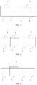
- FIG. 1 is a schematic structural diagram of a device after removal of a hard mask layer in a core region PMOS during a manufacturing process in the related technology.
- FIG. 2 is a schematic structural diagram of the device after deposition of a SiGe layer in the core region PMOS during the manufacturing process in the related technology.
- FIG. 3 is a schematic structural diagram of the device after removal of a hard mask layer during the manufacturing process in the related technology.
- FIG. 4 is a schematic structural diagram of the device after deposition of a thick gate oxide layer during the manufacturing process of a device in the related technology.
- FIG. 5 is a schematic structural diagram of the device after removal of a thick gate oxide layer in a core region during the manufacturing process in the related technology.
- FIG. 6 is a schematic structural diagram of the device after deposition of a thin gate oxide layer during the manufacturing process in the related technology.
- devices in a core region are usually manufactured according to the following method: a hard mask layer 5 on a core region PMOS2 is removed first, to expose the top surface of the core region PMOS2.A SiGe layer 6 is then deposited on the top surface of the core region PMOS2. Then, the hard mask layer 5 on a core region NMOS1, a peripheral region PMOS4, and a peripheral region NMOS3 is removed by wet etching to expose the top surface of the core region NMOS1, the peripheral region PMOS4, and the peripheral region NMOS3. Next, a thick gate oxide layer 7 is deposited on the core region PMOS2, the core region NMOS1, the peripheral region PMOS4, and the peripheral region NMOS3.Then, the thick gate oxide layer 7 on the core region PMOS2 and the core region NMOS1 is removed. Finally, a thin gate oxide layer 8 is deposited on the core region PMOS2 and the core region NMOS1.
- the SiGe layer 6 is damaged when the hard mask layer 5 is removed through wet etching, and the SiGe layer 6 goes through multiple cleaning processes in the subsequent manufacturing, which greatly damages the SiGe layer 6, thus affecting the storage performance of the DRAM device.
- the mask layer is formed on the substrate, to protect structural layers of the array regions and prevent the structural layers of the array region from being damaged; the mask layer on the non-array region is removed to expose the substrate of the non-array region; the first oxide layer is formed on the surface of the substrate of the non-array region, to be used as a barrier layer or insulation layer of the structure on the non-array region; the first oxide layer on the first transistor region is removed to expose the substrate of the first transistor region.
- the first oxide layer can further act as a mask, such that the epitaxial layer is formed on the exposed surface of the substrate of the first transistor region; the first oxide layer on the second transistor region is removed to expose the substrate of the second transistor region, such that the second oxide layer is formed on the surface of the substrate of the second transistor region.
- the epitaxial layer is formed after formation of the first oxide layer.
- the first oxide layer can act as a mask to prevent the epitaxial layer from growing out of the substrate of the first transistor region.
- the damage caused by wet etching of the mask layer to the epitaxial layer can be prevented.
- the epitaxial layer is not provided too early, thus reducing the damage caused by excessive cleaning processes to the epitaxial layer, reducing the damage caused by the method of manufacturing a semiconductor structure to the epitaxial layer, and improving the storage performance of the semiconductor structure.
- FIG. 7 is a schematic flowchart of a method of manufacturing a semiconductor structure according to an embodiment of the present disclosure.
- FIG. 8 is a schematic flowchart of a work function regulating process in the method of manufacturing a semiconductor structure according to an embodiment of the present disclosure.
- FIG. 9 is a schematic structural diagram of a semiconductor structure according to an embodiment of the present disclosure.
- FIG. 10 is a schematic structural diagram after forming of a mask layer in the method of manufacturing a semiconductor structure according to an embodiment of the present disclosure.
- FIG. 11 is a schematic structural diagram after removal of the mask layer in the method of manufacturing a semiconductor structure according to an embodiment of the present disclosure.
- FIG. 12 is a schematic structural diagram after forming of a first oxide layer in the method of manufacturing a semiconductor structure according to an embodiment of the present disclosure.
- FIG. 13 is a schematic structural diagram after removal of the first oxide layer in a first transistor region in the method of manufacturing a semiconductor structure according to an embodiment of the present disclosure.
- FIG. 14 is a schematic structural diagram after forming of an epitaxial layer in the method of manufacturing a semiconductor structure according to an embodiment of the present disclosure.
- FIG. 15 is a schematic structural diagram after removal of the first oxide layer in a second transistor region in the method of manufacturing a semiconductor structure according to an embodiment of the present disclosure.
- FIG. 16 is a schematic structural diagram after forming of a second oxide layer in the method of manufacturing a semiconductor structure according to an embodiment of the present disclosure.
- FIG. 17 is a schematic structural diagram of a mask layer in the method of manufacturing a semiconductor structure according to an embodiment of the present disclosure.
- FIG. 18 is a schematic structural diagram of a second type of mask layer in the method of manufacturing a semiconductor structure according to an embodiment of the present disclosure. With reference to FIG. 7 to FIG. 18 , an embodiment of the present disclosure provides a method of manufacturing
- the method of manufacturing a semiconductor structure specifically includes: S1: Provide a substrate.
- the substrate 10 includes array regions 11 and a non-array region, the non-array region surrounds each of the array regions 11, and the non-array region includes a first transistor region 14 and a second transistor region 15.
- a material of the substrate 10 can be selected from the group consisting of monocrystalline silicon, polycrystalline silicon, amorphous silicon, germanium silicon compound or silicon-on-insulator (SOI), or other materials known to those skilled in the art.
- the substrate 10 can provide support for structural layers on the substrate 10.ln this embodiment, the substrate 10 is a Si substrate.
- the semiconductor structure 100 is as shown in FIG. 9 . It should be noted that FIG. 9 is only a partial schematic structural diagram of the semiconductor structure 100, and does not represent the entire structure of the semiconductor structure 100.
- Multiple array regions 11 can be arranged on the substrate 10; a core region 12 is arranged between adjacent array regions 11; a peripheral region 13 is arranged on the periphery of the core region 12.
- memory cells are arranged in the array regions 11; an induction amplifier and the like are arranged in the core region 12; a peripheral circuit, a driver circuit, a clock circuit and the like are arranged in the peripheral region 13.
- the peripheral region 13 can further include a third transistor region 16 and a fourth transistor region 17.
- the third transistor region 16 and the fourth transistor region 17 can be configured specifically to form a driver circuit, a clock circuit, etc.
- S2 Form a mask layer on the substrate.
- the mask layer 20 By forming the mask layer 20 on the substrate 10, the structural layers of the array regions 11 can be protected, to avoid damage on the structural layers of the array regions 11.
- S4 Form a first oxide layer on the non-array region.
- the first oxide layer 30 is formed on the surface of the substrate 10 of the non-array region.
- the oxide layer 30 can act as a barrier layer or an insulating layer for the structure on the non-array region because the oxide layer can block dirty substances from invading the surface of the substrate 10 on the one hand, and has an insulating effect on the other hand.
- S5 Remove the first oxide layer on the first transistor region, to expose a top surface of the first transistor region.
- the substrate 10 of the first transistor region 14 can be exposed.
- the first oxide layer 30 can further act as a mask, to prevent the epitaxial layer 40 from growing out of the substrate 10 of the first transistor region 14, such that the epitaxial layer 40 is formed on the surface of the exposed substrate 10 of the first transistor region 14.
- S6 Form an epitaxial layer on the top surface of the first transistor region. In this way, structural layers with high carrier mobility can be formed on the substrate 10.
- the epitaxial layer 40 is formed after formation of the first oxide layer 30.
- the first oxide layer 30 can act as a mask.
- the damage caused by removal of the mask layer 20 through wet etching to the epitaxial layer 40 is avoided.
- the forming the epitaxial layer 40 is postponed, such that the epitaxial layer 40 is not provided too early, thus reducing the damage caused by excessive cleaning processes to the epitaxial layer 40, reducing the damage caused by the method of manufacturing a semiconductor structure to the epitaxial layer 40, and improving the storage performance of the semiconductor structure 100.
- the providing a substrate may include: forming a source region, a channel region, and a drain region sequentially arranged in the first transistor region through ion implantation.
- Ion implantation with good controllability and no lateral diffusion, is a preferred doping process for circuits with high density and small critical dimension.
- doping structures can be formed on the substrate 10 by an ion implantation process. During the ion implantation process, the substrate 10 of the channel region can be protected by a mask, and the doping structures can be formed on the substrate 10 of the source region and drain region, thus forming the source region and drain region.
- the non-array region includes a core region 12 and a peripheral region 13.
- the core region 12 is located on the periphery of each of the array regions 11, and the peripheral region 13 is located on the periphery of the core region 12.
- the first transistor region 14 and the second transistor region 15 are both located in the core region 12.
- the removing the first oxide layer on the first transistor region to expose a top surface of the first transistor region may include: removing the first oxide layer located on the channel region located in the first transistor region.
- the first oxide layer 30 can act as a mask on the top surface of the source region and drain region of the first transistor region 14.
- the forming the epitaxial layer on the exposed top surface of the first transistor region may include: forming the epitaxial layer through selective epitaxial growth.
- the epitaxial technology can be used to epitaxially grow a high-resistance epitaxial layer on a low-resistance underlayer, or epitaxially grow a low-resistance epitaxial layer on a high-resistance underlayer, and can also be combined with the mask technology to achieve epitaxial growth in a specified area, which can create conditions for the manufacturing of devices with special structures.
- the compatibility between materials of the epitaxial layer 40 and the substrate 10 should be considered first, where the crystal structure, melting point, vapor pressure, and coefficient of thermal expansion have a great influence on the quality of the epitaxial layer 40; secondly, the contamination of the epitaxial layer 40 caused by the substrate 10 should also be taken into consideration.
- the similar coefficients of thermal expansion of the substrate 10 and the epitaxial layer 40 are one of the important factors to obtain an epitaxial layer 40 with good heterogeneity. If the coefficients of thermal expansion are significantly different, a large stress will be generated near the interface when the temperature changes, which increases the defects of the epitaxial layer 40 and even causes a warp, thus affecting the performance and thermal stability of the material and semiconductor structure.
- the epitaxial layer 40 is SiGe.
- Main epitaxial growth methods include, but are not limited to, gas source molecular beam epitaxy (GSMBE), solid source molecular beam epitaxy (SSMBE) and ultrahigh vacuum chemical vapor deposition (UHV/CVD). GSMBE and UHV/CVD methods are similar, both of which use gas as the source of growth. The main difference is the air pressure in the growth chamber during epitaxy. The air pressure is higher for UHV/CVD growth and lower for GSMBE growth.
- UHV/CVD and GSMBE have obvious advantages over SSMBE in the growth of SiGe materials, e.g., no need for a high-temperature evaporation source furnace, no need to destroy the vacuum of the growth chamber during replacement of the source, thus ensuring the purity of the growth chamber for a long time, facilitating the growth of high-quality materials, and allowing selective epitaxy on the patterned substrate 10.
- the reaction gas is alkane, which contains H, it can also effectively suppress Ge segregation.
- the Ge source is generally GeH 4 , and there are two main types of Si sources: SiH 4 and Si 2 H 6 .
- Si 2 H 6 has a higher adsorption rate and lower reaction energy than SiH 4 on the Si substrate, which is conducive to low-temperature growth, and it is easier to grow high-quality SiGe materials with Si 2 H 6 .
- materials of the epitaxial layer 40 include silicon and germanium, and a content of germanium ranges from 5% to 50%, while the rest of the elements can be all silicon. Specifically, the content of germanium can be 5%, 10%, 17%, 25%, 38%, 44%, 55%, etc. In this way, since the carrier mobility of SiGe is significantly higher than that of Si, the carrier mobility of the epitaxial layer can be increased, to achieve a high current transfer rate of the MOS transistor.
- the embodiments of the present disclosure do not limit the content of germanium. Users can choose within the above range according to the actual situation.
- the Si substrate is first treated to obtain a clean surface in the growth process.
- it is generally possible to first clean the substrate 10 by means of silicon epitaxy to make the substrate 10 clean, and finally treat it with the solution of HCL:H 2 O 2 :H 2 O 1:2:7 or other solutions.
- This aims to form a thin and clean SiO 2 protective layer on the Si surface to prevent the Si surface from being stained before the substrate 10 enters the pretreatment chamber.
- the substrate 10 after the foregoing treatment is fed into the pretreatment chamber and degassed at 300°C for a few hours; then the substrate 10 is fed into the growth chamber and the temperature is raised to 850°C for 10 minutes of deoxidation; after deoxidation, the temperature is lowered to 650°C; the Si 2 H 6 source and GeH 4 source, a ratio between which is adjusted according to a component x, are fed into the growth chamber to grow the Si 1-x Ge x with the component x. Parameters of the cleaning process of the substrate 10 and the preparation process of SiGe can be adjusted as needed in the actual preparation process, which are not limited in this embodiment.
- the epitaxial layer 40 has a thickness in the range of 3 nm to 10 nm, and the thickness can be 3 nm, 5 nm, 7 nm, 8 nm, or 10 nm.
- the above thickness range of the epitaxial layer 40 can ensure high carrier mobility and good performance of the MOS transistor on the one hand, and on the other hand, can make the critical dimension of the semiconductor structure 100 as small as possible.
- the embodiments of the present disclosure do not limit the thickness of the epitaxial layer 40. Users can choose within the above range according to the actual situation.
- the removing the first oxide layer on the second transistor region may include: removing the first oxide layer on the second transistor region, to expose the top surface of the second transistor region. This facilitates deposition of the second oxide layer 50 on the top surface of the second transistor region 15.
- the thickness of the first oxide layer 30 is greater than the thickness of the second oxide layer 50. This allows the first oxide layer 30 to reduce the gate leakage current and the second oxide layer 50 to turn on or to be conductive more easily, such that the first oxide layer 30 and the second oxide layer 50 can be applied to different MOS transistors to achieve different functions.
- the thickness of the first oxide layer 30 ranges from 4 nm to 8 nm, and the specific thickness can be 4 nm, 6 nm, 7 nm, or 8 nm.
- the thickness of the second oxide layer 50 ranges from 0.5 nm to 2 nm, and the specific thickness can be 0.5 nm, 1 nm, 1.5 nm, or 2 nm. The foregoing thickness ranges of the first oxide layer 30 and the second oxide layer 50 ensure that the MOS transistor can reduce the gate leakage current or turn on more easily on the one hand, and on the other hand, can make the critical dimension of the semiconductor structure 100 as small as possible.
- the first oxide layer 30 and the second oxide layer 50 are made of the same material.
- both the first oxide layer 30 and the second oxide layer 50 are silicon dioxide, which is an insulating material that can be used to treat the surface of the Si substrate as a doping barrier, surface insulation layer, and an insulating part in the device.
- silicon dioxide has high density and hardness. Therefore, silicon dioxide can be used as a contamination barrier layer to prevent environmental contaminants from penetrating the sensitive surface of the substrate 10. At the same time, the hardness of silicon dioxide prevents the surface of the substrate 10 from being scratched during the preparation process and also enhances the durability of the substrate 10 during the production process.
- the mask layer 20 can include one layer.
- the material of the mask layer 20 can be silicon dioxide, which on the one hand can protect the sensitive surface of the substrate 10 from environmental contaminants, and on the other hand, the high hardness can prevent the surface of the substrate 10 from being scratched during the preparation process.
- the mask layer 20 can also include multiple stacked sub-mask layers. As shown in FIG. 17 , materials of the mask layer 20 include silicon oxide and silicon nitride, and specifically include two silicon dioxide layers 21 and one silicon nitride layer 22. The silicon nitride layer 22 is located between the two silicon dioxide layers 21. Silicon nitride is a robust mask material that helps to protect the array regions 11.
- the silicon dioxide layers 21 are provided between the silicon nitride layer 22 and the Si substrate, because the silicon nitride layer 22 has high stress; the silicon dioxide layers 21 can be used as a buffer to avoid easy detachment of the silicon nitride layer 22 due to the stress mismatch between the silicon nitride layer 22 and the Si substrate.
- the first mask layer 20 includes multiple layers; as shown in FIG. 18 , the second mask layer 20 includes one layer.
- the method further includes:
- a gate oxide layer may be provided on the second oxide layer 50.
- the work function regulating layer is located on the gate oxide layer, such that work function diffusion particles are diffused to the interface between the gate oxide layer and the second oxide layer 50, and the work function at the interface between the gate oxide layer and the second oxide layer 50 is adjusted by using the work function diffusion particles in the work function regulating layer.
- the work function diffusion particles can include chloride ions or lanthanide ions.
- the method further includes:
- the PMOS transistor and NMOS transistor can be formed in the core region 12, and the critical dimension of the semiconductor structure 100 can be reduced.
- a material of the gate oxide layers of the first transistor structure and the second transistor structure is one or more selected from the group consisting of silicon-doped lanthanum oxide, silicon-doped hafnium oxide, and silicon-doped zirconium oxide.
- the gate oxide layer can reduce the quantum tunneling effect of the gate dielectric layer, thus reducing the gate leakage current of the transistor formed in the semiconductor structure 100 and the consequential high power consumption.
- a material of the gate layers of the first transistor structure and the second transistor structure is selected from the group consisting of titanium, cobalt, aluminum or tungsten.
- the gate layer including the above material can form a metal gate layer.
- the metal gate layer can reduce the threshold voltage drift, polysilicon depletion effect, excessive gate resistance, and Fermi-level pinning of existing polysilicon gates, thereby improving the stability of the semiconductor structure 100 and enhancing the performance of transistors formed in the semiconductor structure 100.
- the semiconductor structure 100 can be manufactured using the manufacturing method described above.
- the semiconductor structure 100 can be a memory, and specifically can include multiple array regions 11 which may be arranged in an array on a substrate 10, a core region 12 between adjacent array regions 11, and a peripheral region 13 on the periphery of the core region 12.An induction amplifier and the like are arranged in the core region 12; a peripheral circuit, a driver circuit, a clock circuit and the like are arranged in the peripheral region 13.
- memory cells are arranged in the array regions 11, and each memory cell includes a capacitor and a transistor. The capacitor is configured to store data, and the transistor can control the access to the data by the capacitor.
- the epitaxial layer 40 is formed after formation of the first oxide layer 30.
- the first oxide layer 30 can serve as a mask.
- the damage caused by removal of the mask layer 20 through wet etching to the epitaxial layer 40 is postponed, such that the epitaxial layer 40 is not provided too early, thus reducing the damage caused by excessive cleaning processes to the epitaxial layer 40, reducing the damage caused by the method of manufacturing a semiconductor structure to the epitaxial layer 40, and improving the storage performance of the semiconductor structure 100.
- connection may be a fixed connection, an indirect connection through an intermediate medium, or internal communication within two elements, or an interactive relationship between two elements.
- a person of ordinary skill in the art may understand specific meanings of the foregoing terms in the present disclosure based on a specific situation. Orientations or position relationships indicated by terms “upper”, “lower”, “front”, “rear”, “vertical”, “horizontal”, “top”, “bottom”, “inside”, “outside”, etc.
- the terms “include”, “contain”, and any other variants mean to cover the non-exclusive inclusion, for example, a process, method, system, product, or device that includes a list of steps or units is not necessarily limited to those steps or units which are clearly listed, but may include other steps or units which are not expressly listed or inherent to such a process, method, system, product, or device.
Landscapes
- Engineering & Computer Science (AREA)
- Manufacturing & Machinery (AREA)
- Metal-Oxide And Bipolar Metal-Oxide Semiconductor Integrated Circuits (AREA)
Abstract
Description
- The present disclosure claims the priority to
Chinese Patent Application 202110469981.4, titled "METHOD OF MANUFACTURING SEMICONDUCTOR STRUCTURE", filed with the China National Intellectual Property Administration (CNIPA) on April 28, 2021 - The present disclosure relates to the technical field of semiconductors, in particular to a method of manufacturing a semiconductor structure.
- The dynamic random access memory (DRAM) is a semiconductor memory that randomly writes and reads data at high speed, and is widely used in data storage devices.
- A DRAM device includes a substrate, which is provided with a peripheral region, a core region, and multiple array regions, where the core region surrounds each of the array regions and the peripheral region surrounds the core region. Memory cells are arranged in the array regions. Each memory cell usually includes a capacitor and a transistor; the gate of the transistor is connected to a word line (WL), the drain is connected to a bit line, and the source is connected to the capacitor. The peripheral region is provided with a driver circuit, a clock circuit, etc. The core region includes a P-type transistor and an N-type transistor, and a SiGe layer is embedded in a channel region of the P-type transistor to increase the carrier mobility, thus improving the storage performance of the DRAM device.
- However, the above method of manufacturing the DRAM device causes a severe damage to the SiGe layer, thus affecting the storage performance of the DRAM device.
- To solve at least one problem mentioned in the background, the present disclosure provides a method of manufacturing a semiconductor structure, which can reduce the damage caused by the method of manufacturing a semiconductor structure to an epitaxial layer, thus improving the storage performance of the semiconductor structure.
- To implement the foregoing objective, the present disclosure provides a method of manufacturing a semiconductor structure, inducing:
- providing a substrate, where the substrate includes an array region and a non-array region, the non-array region surrounds the array region, and the non-array region includes a first transistor region and a second transistor region;
- forming a mask layer on the substrate;
- removing the mask layer on the non-array region;
- forming a first oxide layer on the non-array region;
- removing the first oxide layer on the first transistor region, to expose a top surface of the first transistor region;
- forming an epitaxial layer on the exposed top surface of the first transistor region;
- removing the first oxide layer on the second transistor region; and
- forming a second oxide layer on the second transistor region and the epitaxial layer.
- In the method of manufacturing a semiconductor structure provided by the present disclosure, the mask layer is formed on the substrate, to protect structural layers of the array regions and prevent the structural layers of the array region from being damaged; the mask layer on the non-array region is removed to expose the substrate of the non-array region; the first oxide layer is formed on the surface of the substrate of the non-array region, to be used as a barrier layer or insulation layer of the structure on the non-array region; the first oxide layer on the first transistor region is removed to expose the substrate of the first transistor region. In addition, the first oxide layer can further act as a mask, such that the epitaxial layer is formed on the exposed surface of the substrate of the first transistor region; the first oxide layer on the second transistor region is removed to expose the substrate of the second transistor region, such that the second oxide layer is formed on the surface of the substrate of the second transistor region. In the foregoing manufacturing method, the epitaxial layer is formed after formation of the first oxide layer. On the one hand, the first oxide layer can act as a mask to prevent the epitaxial layer from growing out of the substrate of the first transistor region. On the other hand, the damage caused by removal of the mask layer through wet etching to the epitaxial layer is avoided. In addition, the forming the epitaxial layer is postponed, such that the epitaxial layer is not provided too early, thus reducing the damage caused by excessive cleaning processes to the epitaxial layer, reducing the damage caused by the method of manufacturing a semiconductor structure to the epitaxial layer, and improving the storage performance of the semiconductor structure.
- The structure of the present disclosure and other purposes and beneficial effects of the present disclosure will become easier to understand through description of the exemplary embodiments with reference to the accompanying drawings.
- To describe the technical solutions in the embodiments of the present disclosure or in the prior art more clearly, the following briefly describes the accompanying drawings required for describing the embodiments or the prior art. Apparently, the accompanying drawings in the following description show some embodiments of the present disclosure, and a person of ordinary skill in the art may still derive other drawings from these accompanying drawings without creative efforts.
-
FIG. 1 is a schematic structural diagram of a device after removal of a hard mask layer in a core region PMOS during a manufacturing process in the related technology; -
FIG. 2 is a schematic structural diagram of the device after deposition of a SiGe layer in the core region PMOS during the manufacturing process in the related technology; -
FIG. 3 is a schematic structural diagram of the device after removal of a hard mask layer during the manufacturing process in the related technology; -
FIG. 4 is a schematic structural diagram of the device after deposition of a thick gate oxide layer during the manufacturing process in the related technology; -
FIG. 5 is a schematic structural diagram of the device after removal of a thick gate oxide layer in a core region during the manufacturing process in the related technology; -
FIG. 6 is a schematic structural diagram of the device after deposition of a thin gate oxide layer during the manufacturing process in the related technology; -
FIG. 7 is a schematic flowchart of a method of manufacturing a semiconductor structure according to an embodiment of the present disclosure; -
FIG. 8 is a schematic flowchart of a work function regulating process in the method of manufacturing a semiconductor structure according to an embodiment of the present disclosure; -
FIG. 9 is a schematic structural diagram of a semiconductor structure according to an embodiment of the present disclosure; -
FIG. 10 is a schematic structural diagram after forming of a mask layer in the method of manufacturing a semiconductor structure according to an embodiment of the present disclosure; -
FIG. 11 is a schematic structural diagram after removal of the mask layer in the method of manufacturing a semiconductor structure according to an embodiment of the present disclosure; -
FIG. 12 is a schematic structural diagram after forming of a first oxide layer in the method of manufacturing a semiconductor structure according to an embodiment of the present disclosure; -
FIG. 13 is a schematic structural diagram after removal of the first oxide layer in a first transistor region in the method of manufacturing a semiconductor structure according to an embodiment of the present disclosure; -
FIG. 14 is a schematic structural diagram after forming of an epitaxial layer in the method of manufacturing a semiconductor structure according to an embodiment of the present disclosure; -
FIG. 15 is a schematic structural diagram after removal of the first oxide layer in a second transistor region in the method of manufacturing a semiconductor structure according to an embodiment of the present disclosure; -
FIG. 16 is a schematic structural diagram after forming of a second oxide layer in the method of manufacturing a semiconductor structure according to an embodiment of the present disclosure; -
FIG. 17 is a schematic structural diagram of a first type of mask layer in the method of manufacturing a semiconductor structure according to an embodiment of the present disclosure; and -
FIG. 18 is a schematic structural diagram of a second type of mask layer in the method of manufacturing a semiconductor structure according to an embodiment of the present disclosure. - Description of reference numerals:
1-core region NMOS; 2-core region PMOS; 3-peripheral region NMOS; 4-peripheral region PMOS; 5-hard mask layer; 6-SiGe layer; 7-thick gate oxide layer; 8-thin gate oxide layer; 100-semiconductor structure; 10-substrate; 11-array region; 12-core region; 13-peripheral region; 14-first transistor region; 15-second transistor region; 16-third transistor region; 17-fourth transistor region; 20-mask layer; 21-silicon dioxide layer; 22-silicon nitride layer; 30-first oxide layer; 40-epitaxial layer; 50-second oxide layer. - In the technical field of semiconductor manufacturing, a dynamic random access memory (DRAM) is a semiconductor memory that randomly writes and reads data at a high speed, and is widely used in data storage devices or apparatuses. A DRAM device includes a substrate, which is provided with a peripheral region, a core region, and multiple array regions, where the core region surrounds each of the array regions and the peripheral region surrounds the core region. Memory cells are arranged in the array regions. Each memory cell usually includes a capacitor and a transistor; the gate of the transistor is connected to a word line (WL), the drain is connected to a bit line, and the source is connected to the capacitor. The peripheral region is provided with a driver circuit, a clock circuit, etc. The core region includes a P-type transistor and an N-type transistor, and a SiGe layer is generally embedded in a channel region of the P-type transistor to increase the carrier mobility, thus improving the storage performance of the DRAM device.
- Specifically,
FIG. 1 is a schematic structural diagram of a device after removal of a hard mask layer in a core region PMOS during a manufacturing process in the related technology.FIG. 2 is a schematic structural diagram of the device after deposition of a SiGe layer in the core region PMOS during the manufacturing process in the related technology.FIG. 3 is a schematic structural diagram of the device after removal of a hard mask layer during the manufacturing process in the related technology.FIG. 4 is a schematic structural diagram of the device after deposition of a thick gate oxide layer during the manufacturing process of a device in the related technology.FIG. 5 is a schematic structural diagram of the device after removal of a thick gate oxide layer in a core region during the manufacturing process in the related technology.FIG. 6 is a schematic structural diagram of the device after deposition of a thin gate oxide layer during the manufacturing process in the related technology. - As shown in
FIG. 1 to FIG. 6 , in the related technology, devices in a core region are usually manufactured according to the following method: ahard mask layer 5 on a core region PMOS2 is removed first, to expose the top surface of the core region PMOS2.ASiGe layer 6 is then deposited on the top surface of the core region PMOS2.Then, thehard mask layer 5 on a core region NMOS1, a peripheral region PMOS4, and a peripheral region NMOS3 is removed by wet etching to expose the top surface of the core region NMOS1, the peripheral region PMOS4, and the peripheral region NMOS3.Next, a thickgate oxide layer 7 is deposited on the core region PMOS2, the core region NMOS1, the peripheral region PMOS4, and the peripheral region NMOS3.Then, the thickgate oxide layer 7 on the core region PMOS2 and the core region NMOS1 is removed. Finally, a thingate oxide layer 8 is deposited on the core region PMOS2 and the core region NMOS1. - However, in the foregoing manufacturing method, after deposition of the
SiGe layer 6, theSiGe layer 6 is damaged when thehard mask layer 5 is removed through wet etching, and theSiGe layer 6 goes through multiple cleaning processes in the subsequent manufacturing, which greatly damages theSiGe layer 6, thus affecting the storage performance of the DRAM device. - Accordingly, the method of manufacturing a semiconductor structure provided by the present disclosure, the mask layer is formed on the substrate, to protect structural layers of the array regions and prevent the structural layers of the array region from being damaged; the mask layer on the non-array region is removed to expose the substrate of the non-array region; the first oxide layer is formed on the surface of the substrate of the non-array region, to be used as a barrier layer or insulation layer of the structure on the non-array region; the first oxide layer on the first transistor region is removed to expose the substrate of the first transistor region. In addition, the first oxide layer can further act as a mask, such that the epitaxial layer is formed on the exposed surface of the substrate of the first transistor region; the first oxide layer on the second transistor region is removed to expose the substrate of the second transistor region, such that the second oxide layer is formed on the surface of the substrate of the second transistor region. In the foregoing manufacturing method, the epitaxial layer is formed after formation of the first oxide layer. On the one hand, the first oxide layer can act as a mask to prevent the epitaxial layer from growing out of the substrate of the first transistor region. On the other hand, the damage caused by wet etching of the mask layer to the epitaxial layer can be prevented. In addition, after the forming the epitaxial layer, the epitaxial layer is not provided too early, thus reducing the damage caused by excessive cleaning processes to the epitaxial layer, reducing the damage caused by the method of manufacturing a semiconductor structure to the epitaxial layer, and improving the storage performance of the semiconductor structure.
- In order to make the objectives, technical solutions and advantages of the embodiments of the present disclosure clearer, the technical solutions in the embodiments of the present disclosure are described in further detail below with reference to the accompanying drawings in the exemplary embodiments of the present disclosure. In the drawings, the same or similar numerals represent the same or similar elements or elements having the same or similar functions throughout the specification. The described embodiments are some rather than all of the embodiments of the present disclosure. The embodiments described below with reference to the accompanying drawings are exemplary, and are only used to explain the present disclosure but should not be construed as a limitation to the present disclosure. All other embodiments obtained by those of ordinary skill in the art based on the embodiments of the present disclosure without creative efforts should fall within the protection scope of the present disclosure. The embodiments of the present disclosure are described in detail below with reference to the drawings.
-
FIG. 7 is a schematic flowchart of a method of manufacturing a semiconductor structure according to an embodiment of the present disclosure.FIG. 8 is a schematic flowchart of a work function regulating process in the method of manufacturing a semiconductor structure according to an embodiment of the present disclosure.FIG. 9 is a schematic structural diagram of a semiconductor structure according to an embodiment of the present disclosure.FIG. 10 is a schematic structural diagram after forming of a mask layer in the method of manufacturing a semiconductor structure according to an embodiment of the present disclosure.FIG. 11 is a schematic structural diagram after removal of the mask layer in the method of manufacturing a semiconductor structure according to an embodiment of the present disclosure.FIG. 12 is a schematic structural diagram after forming of a first oxide layer in the method of manufacturing a semiconductor structure according to an embodiment of the present disclosure.FIG. 13 is a schematic structural diagram after removal of the first oxide layer in a first transistor region in the method of manufacturing a semiconductor structure according to an embodiment of the present disclosure.FIG. 14 is a schematic structural diagram after forming of an epitaxial layer in the method of manufacturing a semiconductor structure according to an embodiment of the present disclosure.FIG. 15 is a schematic structural diagram after removal of the first oxide layer in a second transistor region in the method of manufacturing a semiconductor structure according to an embodiment of the present disclosure.FIG. 16 is a schematic structural diagram after forming of a second oxide layer in the method of manufacturing a semiconductor structure according to an embodiment of the present disclosure.FIG. 17 is a schematic structural diagram of a mask layer in the method of manufacturing a semiconductor structure according to an embodiment of the present disclosure.FIG. 18 is a schematic structural diagram of a second type of mask layer in the method of manufacturing a semiconductor structure according to an embodiment of the present disclosure. With reference toFIG. 7 to FIG. 18 , an embodiment of the present disclosure provides a method of manufacturing a semiconductor structure. - As shown in
FIG. 7 , the method of manufacturing a semiconductor structure specifically includes:
S1: Provide a substrate. Thesubstrate 10 includesarray regions 11 and a non-array region, the non-array region surrounds each of thearray regions 11, and the non-array region includes afirst transistor region 14 and asecond transistor region 15. - It should be noted that a material of the
substrate 10 can be selected from the group consisting of monocrystalline silicon, polycrystalline silicon, amorphous silicon, germanium silicon compound or silicon-on-insulator (SOI), or other materials known to those skilled in the art. Thesubstrate 10 can provide support for structural layers on the substrate 10.ln this embodiment, thesubstrate 10 is a Si substrate. - The
semiconductor structure 100 is as shown inFIG. 9 . It should be noted thatFIG. 9 is only a partial schematic structural diagram of thesemiconductor structure 100, and does not represent the entire structure of thesemiconductor structure 100.Multiple array regions 11 can be arranged on thesubstrate 10; acore region 12 is arranged betweenadjacent array regions 11; aperipheral region 13 is arranged on the periphery of thecore region 12. Generally, memory cells are arranged in thearray regions 11; an induction amplifier and the like are arranged in thecore region 12; a peripheral circuit, a driver circuit, a clock circuit and the like are arranged in the peripheral region 13.ln addition, theperipheral region 13 can further include athird transistor region 16 and afourth transistor region 17. Thethird transistor region 16 and thefourth transistor region 17 can be configured specifically to form a driver circuit, a clock circuit, etc. - S2: Form a mask layer on the substrate. By forming the
mask layer 20 on thesubstrate 10, the structural layers of thearray regions 11 can be protected, to avoid damage on the structural layers of thearray regions 11. - S3: Remove the mask layer on the non-array region. This allows the
substrate 10 of the non-array region to be exposed, such that afirst oxide layer 30 can be formed. - S4: Form a first oxide layer on the non-array region. The
first oxide layer 30 is formed on the surface of thesubstrate 10 of the non-array region. Theoxide layer 30 can act as a barrier layer or an insulating layer for the structure on the non-array region because the oxide layer can block dirty substances from invading the surface of thesubstrate 10 on the one hand, and has an insulating effect on the other hand. - S5: Remove the first oxide layer on the first transistor region, to expose a top surface of the first transistor region. By removing the
first oxide layer 30 on thefirst transistor region 14, thesubstrate 10 of thefirst transistor region 14 can be exposed. In addition, thefirst oxide layer 30 can further act as a mask, to prevent theepitaxial layer 40 from growing out of thesubstrate 10 of thefirst transistor region 14, such that theepitaxial layer 40 is formed on the surface of the exposedsubstrate 10 of thefirst transistor region 14. - S6: Form an epitaxial layer on the top surface of the first transistor region. In this way, structural layers with high carrier mobility can be formed on the
substrate 10. - S7: Remove the first oxide layer on the second transistor region. In this way, the
substrate 10 of thesecond transistor region 15 can be exposed, such that asecond oxide layer 50 is formed on the surface of thesubstrate 10 of thesecond transistor region 15. - S8: Form a second oxide layer on the second transistor region and the epitaxial layer.
- Specifically, for the structure after each step, refer to
FIG. 10 to FIG. 16 . In the foregoing manufacturing method, theepitaxial layer 40 is formed after formation of thefirst oxide layer 30. On the one hand, thefirst oxide layer 30 can act as a mask. On the other hand, the damage caused by removal of themask layer 20 through wet etching to theepitaxial layer 40 is avoided. In addition, the forming theepitaxial layer 40 is postponed, such that theepitaxial layer 40 is not provided too early, thus reducing the damage caused by excessive cleaning processes to theepitaxial layer 40, reducing the damage caused by the method of manufacturing a semiconductor structure to theepitaxial layer 40, and improving the storage performance of thesemiconductor structure 100. - In one possible implementation, the providing a substrate may include: forming a source region, a channel region, and a drain region sequentially arranged in the first transistor region through ion implantation. Ion implantation, with good controllability and no lateral diffusion, is a preferred doping process for circuits with high density and small critical dimension. Specifically, doping structures can be formed on the
substrate 10 by an ion implantation process. During the ion implantation process, thesubstrate 10 of the channel region can be protected by a mask, and the doping structures can be formed on thesubstrate 10 of the source region and drain region, thus forming the source region and drain region. - Specifically, the non-array region includes a
core region 12 and aperipheral region 13. Thecore region 12 is located on the periphery of each of thearray regions 11, and theperipheral region 13 is located on the periphery of thecore region 12. Thefirst transistor region 14 and thesecond transistor region 15 are both located in thecore region 12. Such an arrangement facilitates the installation of induction amplifiers, driver circuits, clock circuits, etc., and helps to reduce the critical dimension of thesemiconductor structure 100. - In a possible implementation, the removing the first oxide layer on the first transistor region to expose a top surface of the first transistor region may include: removing the first oxide layer located on the channel region located in the first transistor region. On the one hand, it is possible to form a groove in the top surface of the channel region and expose the surface of the
substrate 10 to facilitate epitaxial growth of theepitaxial layer 40. On the other hand, thefirst oxide layer 30 can act as a mask on the top surface of the source region and drain region of thefirst transistor region 14. - In a possible implementation, the forming the epitaxial layer on the exposed top surface of the first transistor region may include: forming the epitaxial layer through selective epitaxial growth.
- It should be noted that the epitaxial technology can be used to epitaxially grow a high-resistance epitaxial layer on a low-resistance underlayer, or epitaxially grow a low-resistance epitaxial layer on a high-resistance underlayer, and can also be combined with the mask technology to achieve epitaxial growth in a specified area, which can create conditions for the manufacturing of devices with special structures. In the epitaxial process, the compatibility between materials of the
epitaxial layer 40 and thesubstrate 10 should be considered first, where the crystal structure, melting point, vapor pressure, and coefficient of thermal expansion have a great influence on the quality of theepitaxial layer 40; secondly, the contamination of theepitaxial layer 40 caused by thesubstrate 10 should also be taken into consideration. On the other hand, the similar coefficients of thermal expansion of thesubstrate 10 and theepitaxial layer 40 are one of the important factors to obtain anepitaxial layer 40 with good heterogeneity. If the coefficients of thermal expansion are significantly different, a large stress will be generated near the interface when the temperature changes, which increases the defects of theepitaxial layer 40 and even causes a warp, thus affecting the performance and thermal stability of the material and semiconductor structure. - Specifically, in the embodiment of the present disclosure, the
epitaxial layer 40 is SiGe. Main epitaxial growth methods include, but are not limited to, gas source molecular beam epitaxy (GSMBE), solid source molecular beam epitaxy (SSMBE) and ultrahigh vacuum chemical vapor deposition (UHV/CVD). GSMBE and UHV/CVD methods are similar, both of which use gas as the source of growth. The main difference is the air pressure in the growth chamber during epitaxy. The air pressure is higher for UHV/CVD growth and lower for GSMBE growth. UHV/CVD and GSMBE have obvious advantages over SSMBE in the growth of SiGe materials, e.g., no need for a high-temperature evaporation source furnace, no need to destroy the vacuum of the growth chamber during replacement of the source, thus ensuring the purity of the growth chamber for a long time, facilitating the growth of high-quality materials, and allowing selective epitaxy on the patternedsubstrate 10. Because the reaction gas is alkane, which contains H, it can also effectively suppress Ge segregation. For the growth of SiGe by UHV/CVD and GSMBE, the Ge source is generally GeH4, and there are two main types of Si sources: SiH4 and Si2H6. In particular, Si2H6 has a higher adsorption rate and lower reaction energy than SiH4 on the Si substrate, which is conducive to low-temperature growth, and it is easier to grow high-quality SiGe materials with Si2H6. - Specifically, materials of the
epitaxial layer 40 include silicon and germanium, and a content of germanium ranges from 5% to 50%, while the rest of the elements can be all silicon. Specifically, the content of germanium can be 5%, 10%, 17%, 25%, 38%, 44%, 55%, etc. In this way, since the carrier mobility of SiGe is significantly higher than that of Si, the carrier mobility of the epitaxial layer can be increased, to achieve a high current transfer rate of the MOS transistor. The embodiments of the present disclosure do not limit the content of germanium. Users can choose within the above range according to the actual situation. - It should be noted that the Si substrate is first treated to obtain a clean surface in the growth process. As a possible implementation, it is generally possible to first clean the
substrate 10 by means of silicon epitaxy to make thesubstrate 10 clean, and finally treat it with the solution of HCL:H2O2:H2O=1:2:7 or other solutions. This aims to form a thin and clean SiO2 protective layer on the Si surface to prevent the Si surface from being stained before thesubstrate 10 enters the pretreatment chamber. Thesubstrate 10 after the foregoing treatment is fed into the pretreatment chamber and degassed at 300°C for a few hours; then thesubstrate 10 is fed into the growth chamber and the temperature is raised to 850°C for 10 minutes of deoxidation; after deoxidation, the temperature is lowered to 650°C; the Si2H6 source and GeH4 source, a ratio between which is adjusted according to a component x, are fed into the growth chamber to grow the Si1-xGex with the component x. Parameters of the cleaning process of thesubstrate 10 and the preparation process of SiGe can be adjusted as needed in the actual preparation process, which are not limited in this embodiment. - Specifically, the
epitaxial layer 40 has a thickness in the range of 3 nm to 10 nm, and the thickness can be 3 nm, 5 nm, 7 nm, 8 nm, or 10 nm. The above thickness range of theepitaxial layer 40 can ensure high carrier mobility and good performance of the MOS transistor on the one hand, and on the other hand, can make the critical dimension of thesemiconductor structure 100 as small as possible. The embodiments of the present disclosure do not limit the thickness of theepitaxial layer 40. Users can choose within the above range according to the actual situation. - In one possible implementation, the removing the first oxide layer on the second transistor region may include: removing the first oxide layer on the second transistor region, to expose the top surface of the second transistor region. This facilitates deposition of the
second oxide layer 50 on the top surface of thesecond transistor region 15. - Specifically, the thickness of the
first oxide layer 30 is greater than the thickness of thesecond oxide layer 50. This allows thefirst oxide layer 30 to reduce the gate leakage current and thesecond oxide layer 50 to turn on or to be conductive more easily, such that thefirst oxide layer 30 and thesecond oxide layer 50 can be applied to different MOS transistors to achieve different functions. - Specifically, the thickness of the
first oxide layer 30 ranges from 4 nm to 8 nm, and the specific thickness can be 4 nm, 6 nm, 7 nm, or 8 nm. In a possible implementation, the thickness of thesecond oxide layer 50 ranges from 0.5 nm to 2 nm, and the specific thickness can be 0.5 nm, 1 nm, 1.5 nm, or 2 nm. The foregoing thickness ranges of thefirst oxide layer 30 and thesecond oxide layer 50 ensure that the MOS transistor can reduce the gate leakage current or turn on more easily on the one hand, and on the other hand, can make the critical dimension of thesemiconductor structure 100 as small as possible. - Specifically, the
first oxide layer 30 and thesecond oxide layer 50 are made of the same material. In the embodiments of the present disclosure, both thefirst oxide layer 30 and thesecond oxide layer 50 are silicon dioxide, which is an insulating material that can be used to treat the surface of the Si substrate as a doping barrier, surface insulation layer, and an insulating part in the device. - It should be noted that silicon dioxide has high density and hardness. Therefore, silicon dioxide can be used as a contamination barrier layer to prevent environmental contaminants from penetrating the sensitive surface of the
substrate 10. At the same time, the hardness of silicon dioxide prevents the surface of thesubstrate 10 from being scratched during the preparation process and also enhances the durability of thesubstrate 10 during the production process. - Specifically, the
mask layer 20 can include one layer. When themask layer 20 includes one layer, the material of themask layer 20 can be silicon dioxide, which on the one hand can protect the sensitive surface of thesubstrate 10 from environmental contaminants, and on the other hand, the high hardness can prevent the surface of thesubstrate 10 from being scratched during the preparation process. Themask layer 20 can also include multiple stacked sub-mask layers. As shown inFIG. 17 , materials of themask layer 20 include silicon oxide and silicon nitride, and specifically include two silicon dioxide layers 21 and onesilicon nitride layer 22. Thesilicon nitride layer 22 is located between the two silicon dioxide layers 21. Silicon nitride is a robust mask material that helps to protect thearray regions 11. The silicon dioxide layers 21 are provided between thesilicon nitride layer 22 and the Si substrate, because thesilicon nitride layer 22 has high stress; the silicon dioxide layers 21 can be used as a buffer to avoid easy detachment of thesilicon nitride layer 22 due to the stress mismatch between thesilicon nitride layer 22 and the Si substrate. As shown inFIG. 17 , thefirst mask layer 20 includes multiple layers; as shown inFIG. 18 , thesecond mask layer 20 includes one layer. - In one possible implementation, as shown in
FIG. 2 , after the forming a second oxide layer on the second transistor region and the epitaxial layer, the method further includes: - S9: Form a work function regulating layer on the second oxide layer.
- S10: Anneal the second oxide layer and the work function regulating layer, where the second oxide layer forms a gate oxide layer.
- S11: Remove the work function regulating layer.
- It should be noted that, a gate oxide layer may be provided on the
second oxide layer 50. The work function regulating layer is located on the gate oxide layer, such that work function diffusion particles are diffused to the interface between the gate oxide layer and thesecond oxide layer 50, and the work function at the interface between the gate oxide layer and thesecond oxide layer 50 is adjusted by using the work function diffusion particles in the work function regulating layer. The work function diffusion particles can include chloride ions or lanthanide ions. - Specifically, after the removing the work function regulating layer, the method further includes:
- forming a first transistor structure on the surface of the first transistor region, where the first transistor structure is a P-type transistor; and
- forming a second transistor structure on the surface of the second transistor region, where the second transistor structure is an N-type transistor.
- In this way, the PMOS transistor and NMOS transistor can be formed in the
core region 12, and the critical dimension of thesemiconductor structure 100 can be reduced. - Specifically, a material of the gate oxide layers of the first transistor structure and the second transistor structure is one or more selected from the group consisting of silicon-doped lanthanum oxide, silicon-doped hafnium oxide, and silicon-doped zirconium oxide. The gate oxide layer can reduce the quantum tunneling effect of the gate dielectric layer, thus reducing the gate leakage current of the transistor formed in the
semiconductor structure 100 and the consequential high power consumption. - In addition, a material of the gate layers of the first transistor structure and the second transistor structure is selected from the group consisting of titanium, cobalt, aluminum or tungsten. The gate layer including the above material can form a metal gate layer. The metal gate layer can reduce the threshold voltage drift, polysilicon depletion effect, excessive gate resistance, and Fermi-level pinning of existing polysilicon gates, thereby improving the stability of the
semiconductor structure 100 and enhancing the performance of transistors formed in thesemiconductor structure 100. - On the basis of the above, this embodiment further provides a semiconductor structure. The
semiconductor structure 100 can be manufactured using the manufacturing method described above. Thesemiconductor structure 100 can be a memory, and specifically can includemultiple array regions 11 which may be arranged in an array on asubstrate 10, acore region 12 betweenadjacent array regions 11, and aperipheral region 13 on the periphery of the core region 12.An induction amplifier and the like are arranged in thecore region 12; a peripheral circuit, a driver circuit, a clock circuit and the like are arranged in the peripheral region 13.Generally, memory cells are arranged in thearray regions 11, and each memory cell includes a capacitor and a transistor. The capacitor is configured to store data, and the transistor can control the access to the data by the capacitor. - In the
semiconductor structure 100 provided by the present disclosure, theepitaxial layer 40 is formed after formation of thefirst oxide layer 30. On the one hand, thefirst oxide layer 30 can serve as a mask. On the other hand, the damage caused by removal of themask layer 20 through wet etching to theepitaxial layer 40. In addition, the forming theepitaxial layer 40 is postponed, such that theepitaxial layer 40 is not provided too early, thus reducing the damage caused by excessive cleaning processes to theepitaxial layer 40, reducing the damage caused by the method of manufacturing a semiconductor structure to theepitaxial layer 40, and improving the storage performance of thesemiconductor structure 100. - In the description, it should be noted that unless otherwise expressly specified and defined, terms such as "mounted", "connected to each other", and "connected to" should be comprehended in a broad sense. For example, a connection may be a fixed connection, an indirect connection through an intermediate medium, or internal communication within two elements, or an interactive relationship between two elements. A person of ordinary skill in the art may understand specific meanings of the foregoing terms in the present disclosure based on a specific situation. Orientations or position relationships indicated by terms "upper", "lower", "front", "rear", "vertical", "horizontal", "top", "bottom", "inside", "outside", etc. are orientation or position relationships as shown in the drawings, and these terms are just used to facilitate description of the present disclosure and simplify the description, but not to indicate or imply that the mentioned device or elements must have a specific orientation and must be established and operated in a specific orientation, and thus, these terms cannot be understood as a limitation to the present disclosure. In the description of the present disclosure, "a plurality of" means two or more, unless otherwise specifically defined.
- The terms "first", "second", "third" and so on (if any) in the specification, claims and the accompanying drawings of the present disclosure are intended to distinguish between similar objects but do not necessarily indicate a specific order or sequence. It should be understood that the data used in such a way may be exchanged under proper conditions to make it possible to implement the described embodiments of the present disclosure in other sequences apart from those illustrated or described here. Moreover, the terms "include", "contain", and any other variants mean to cover the non-exclusive inclusion, for example, a process, method, system, product, or device that includes a list of steps or units is not necessarily limited to those steps or units which are clearly listed, but may include other steps or units which are not expressly listed or inherent to such a process, method, system, product, or device.
- Finally, it should be noted that the above embodiments are merely used to explain the technical solutions of the present disclosure, but are not intended to limit the present disclosure. Although the present disclosure is described in detail with reference to the foregoing embodiments, those of ordinary skill in the art should understand that they can still modify the technical solutions described in the foregoing embodiments, or make equivalent substitutions on some or all technical features therein. These modifications or substitutions do not make the essence of the corresponding technical solutions deviate from the spirit and scope of the technical solutions of the embodiments of the present disclosure.
Claims (15)
- A method of manufacturing a semiconductor structure, comprising:providing a substrate, wherein the substrate comprises an array region and a non-array region, the non-array region surrounds the array region, and the non-array region comprises a first transistor region and a second transistor region;forming a mask layer on the substrate;removing the mask layer on the non-array region;forming a first oxide layer on the non-array region;removing the first oxide layer on the first transistor region, to expose a top surface of the first transistor region;forming an epitaxial layer on the exposed top surface of the first transistor region;removing the first oxide layer on the second transistor region; andforming a second oxide layer on the second transistor region and the epitaxial layer.
- The method of manufacturing a semiconductor structure according to claim 1, wherein the providing a substrate comprises:
forming a source region, a channel region, and a drain region sequentially arranged in the first transistor region through ion implantation. - The method of manufacturing a semiconductor structure according to claim 2, wherein the non-array region comprises a core region and a peripheral region, the core region is located on the periphery of the array region, and the peripheral region is located on the periphery of the core region; and
the first transistor region and the second transistor region are both located in the core region. - The method of manufacturing a semiconductor structure according to claim 2, wherein the removing the first oxide layer on the first transistor region, to expose a top surface of the first transistor region comprises:
removing the first oxide layer located on the channel region in the first transistor region. - The method of manufacturing a semiconductor structure according to any one of claims 1 to 4, wherein the forming an epitaxial layer on the exposed top surface of the first transistor region comprises:
forming the epitaxial layer through selective epitaxial growth. - The method of manufacturing a semiconductor structure according to any one of claims 1 to 4, wherein materials of the epitaxial layer comprise silicon and germanium, and a content of germanium ranges from 5% to 50%.
- The method of manufacturing a semiconductor structure according to any one of claims 1 to 4, wherein the epitaxial layer has a thickness in the range of 3 nm to 10 nm.
- The method of manufacturing a semiconductor structure according to claim 3, wherein the removing the first oxide layer on the second transistor region comprises:
removing the first oxide layer on the second transistor region, to expose a top surface of the second transistor region. - The method of manufacturing a semiconductor structure according to any one of claims 1 to 4, wherein a thickness of the first oxide layer is greater than a thickness of the second oxide layer.
- The method of manufacturing a semiconductor structure according to claim 9, wherein the thickness of the first oxide layer ranges from 4 nm to 8 nm; and/or
the thickness of the second oxide layer ranges from 0.5 nm to 2 nm. - The method of manufacturing a semiconductor structure according to any one of claims 1 to 4, wherein the first oxide layer and the second oxide layer are made of the same material.
- The method of manufacturing a semiconductor structure according to any one of claims 1 to 4, wherein the mask layer is a single layer, or the mask layer comprises multiple stacked sub-mask layers; and/or
materials of the mask layer comprise silicon oxide and silicon nitride. - The method of manufacturing a semiconductor structure according to any one of claims 1 to 4, after the forming a second oxide layer on the second transistor region and the epitaxial layer, the method further comprises:forming a work function regulating layer on the second oxide layer;annealing the second oxide layer and the work function regulating layer, wherein the second oxide layer forms a gate oxide layer; andremoving the work function regulating layer.
- The method of manufacturing a semiconductor structure according to claim 13, after the removing the work function regulating layer, the method further comprises:forming a first transistor structure on a surface of the first transistor region, wherein the first transistor structure is a P-type transistor; andforming a second transistor structure on a surface of the second transistor region, wherein the second transistor structure is an N-type transistor.
- The method of manufacturing a semiconductor structure according to claim 14, wherein a material of gate oxide layers of the first transistor structure and the second transistor structure is one or more selected from the group consisting of silicon-doped lanthanum oxide, silicon-doped hafnium oxide, and silicon-doped zirconium oxide; and/or
a material of gate layers of the first transistor structure and the second transistor structure is selected from the group consisting of titanium, cobalt, aluminum and tungsten.
Applications Claiming Priority (2)
| Application Number | Priority Date | Filing Date | Title |
|---|---|---|---|
| CN202110469981.4A CN115249655A (en) | 2021-04-28 | 2021-04-28 | Preparation method of semiconductor structure |
| PCT/CN2021/111890 WO2022227338A1 (en) | 2021-04-28 | 2021-08-10 | Preparation method for semiconductor structure |
Publications (2)
| Publication Number | Publication Date |
|---|---|
| EP4120333A1 true EP4120333A1 (en) | 2023-01-18 |
| EP4120333A4 EP4120333A4 (en) | 2023-10-25 |
Family
ID=83807819
Family Applications (1)
| Application Number | Title | Priority Date | Filing Date |
|---|---|---|---|
| EP21935429.7A Withdrawn EP4120333A4 (en) | 2021-04-28 | 2021-08-10 | METHOD FOR PREPARING SEMICONDUCTOR STRUCTURE |
Country Status (2)
| Country | Link |
|---|---|
| US (1) | US12464700B2 (en) |
| EP (1) | EP4120333A4 (en) |
Family Cites Families (16)
| Publication number | Priority date | Publication date | Assignee | Title |
|---|---|---|---|---|
| EP0996152A1 (en) | 1998-10-23 | 2000-04-26 | STMicroelectronics S.r.l. | Process for manufacturing electronic devices comprising non-salicidated nonvolatile memory cells, non-salicidated HV transistors, and salicidated-junction LV transistors |
| US6150234A (en) * | 1999-12-16 | 2000-11-21 | Vlsi Technology, Inc. | Trench-diffusion corner rounding in a shallow-trench (STI) process |
| JP3481902B2 (en) | 2000-05-30 | 2003-12-22 | 株式会社東芝 | Method for manufacturing TFT array |
| JP2001351989A (en) * | 2000-06-05 | 2001-12-21 | Nec Corp | Method for manufacturing semiconductor device |
| JP4034627B2 (en) * | 2001-09-28 | 2008-01-16 | テキサス インスツルメンツ インコーポレイテツド | Integrated circuit and manufacturing method thereof |
| US6770521B2 (en) * | 2001-11-30 | 2004-08-03 | Texas Instruments Incorporated | Method of making multiple work function gates by implanting metals with metallic alloying additives |
| US6909147B2 (en) * | 2003-05-05 | 2005-06-21 | International Business Machines Corporation | Multi-height FinFETS |
| US7202535B2 (en) | 2005-07-14 | 2007-04-10 | Infineon Technologies Ag | Manufacturing method for an integrated semiconductor structure and corresponding integrated semiconductor structure |
| JP4966153B2 (en) * | 2007-10-05 | 2012-07-04 | 株式会社東芝 | Field effect transistor and manufacturing method thereof |
| US7833891B2 (en) * | 2008-07-23 | 2010-11-16 | International Business Machines Corporation | Semiconductor device manufacturing method using oxygen diffusion barrier layer between buried oxide layer and high K dielectric layer |
| KR101486425B1 (en) * | 2008-11-19 | 2015-01-27 | 삼성전자주식회사 | Method for manufacturing dual gate semiconductor device |
| JP2010287716A (en) * | 2009-06-11 | 2010-12-24 | Elpida Memory Inc | Semiconductor device and manufacturing method thereof |
| KR20120054935A (en) * | 2010-11-22 | 2012-05-31 | 삼성전자주식회사 | Semiconductor device employing high-k dielectric layers as a gate insulating layer and methods of fabricating the same |
| KR101186038B1 (en) * | 2010-11-26 | 2012-09-26 | 에스케이하이닉스 주식회사 | Method of fabricating semiconductor device |
| CN105826376B (en) | 2015-01-07 | 2019-01-22 | 中芯国际集成电路制造(上海)有限公司 | Semiconductor devices, the method for preparing semiconductor devices |
| CN112599593B (en) | 2020-12-11 | 2023-01-13 | 上海交通大学 | Graphene-based field effect transistor preparation system and preparation method |
-
2021
- 2021-08-10 EP EP21935429.7A patent/EP4120333A4/en not_active Withdrawn
-
2022
- 2022-02-18 US US17/651,577 patent/US12464700B2/en active Active
Also Published As
| Publication number | Publication date |
|---|---|
| US12464700B2 (en) | 2025-11-04 |
| US20220352175A1 (en) | 2022-11-03 |
| EP4120333A4 (en) | 2023-10-25 |
Similar Documents
| Publication | Publication Date | Title |
|---|---|---|
| KR102892295B1 (en) | Electronic device and method of manufacturing the same | |
| US6437375B1 (en) | PD-SOI substrate with suppressed floating body effect and method for its fabrication | |
| EP0383230B1 (en) | Manufacturing Method of a Semiconductor Device | |
| US7176109B2 (en) | Method for forming raised structures by controlled selective epitaxial growth of facet using spacer | |
| US6399429B1 (en) | Method of forming monocrystalline silicon layer, method for manufacturing semiconductor device, and semiconductor device | |
| US20060094169A1 (en) | Semiconductor device structure and method therefor | |
| US20150171165A1 (en) | Bonded strained semiconductor with a desired surface orientation and conductance direction | |
| US20150001623A1 (en) | Field effect transistor and method for forming the same | |
| US10192887B2 (en) | Method to improve crystalline regrowth | |
| US7432141B2 (en) | Large-grain p-doped polysilicon films for use in thin film transistors | |
| US20230055158A1 (en) | Semiconductor isolation bridge for three-dimensional dynamic random-access memory | |
| TW557568B (en) | Semiconductor integrated circuit device and method of manufacturing the same | |
| US12464700B2 (en) | Method of manufacturing semiconductor structure | |
| US20120241866A1 (en) | Transistor structure and manufacturing method which has channel epitaxial equipped with lateral epitaxial structure | |
| WO2022227338A1 (en) | Preparation method for semiconductor structure | |
| US20070158734A1 (en) | Electronic device with a multi-gated electrode structure and a process for forming the electronic device | |
| US11075081B2 (en) | Semiconductor device with multiple threshold voltages | |
| CN116031208B (en) | Semiconductor structure and its formation method | |
| US20260047064A1 (en) | Sacrificial metal signal or power line | |
| KR20010066393A (en) | Method for Manufacturing of Thin Film Trunsistor | |
| KR20030047571A (en) | Method of Forming Silicon Thin Film | |
| KR20050104227A (en) | Method for forming contact plug of semiconductor device | |
| HK1014293B (en) | A method of manufacturing a semiconductor device |
Legal Events
| Date | Code | Title | Description |
|---|---|---|---|
| STAA | Information on the status of an ep patent application or granted ep patent |
Free format text: STATUS: UNKNOWN |
|
| STAA | Information on the status of an ep patent application or granted ep patent |
Free format text: STATUS: THE INTERNATIONAL PUBLICATION HAS BEEN MADE |
|
| PUAI | Public reference made under article 153(3) epc to a published international application that has entered the european phase |
Free format text: ORIGINAL CODE: 0009012 |
|
| STAA | Information on the status of an ep patent application or granted ep patent |
Free format text: STATUS: REQUEST FOR EXAMINATION WAS MADE |
|
| 17P | Request for examination filed |
Effective date: 20221011 |
|
| AK | Designated contracting states |
Kind code of ref document: A1 Designated state(s): AL AT BE BG CH CY CZ DE DK EE ES FI FR GB GR HR HU IE IS IT LI LT LU LV MC MK MT NL NO PL PT RO RS SE SI SK SM TR |
|
| A4 | Supplementary search report drawn up and despatched |
Effective date: 20230926 |
|
| RIC1 | Information provided on ipc code assigned before grant |
Ipc: H01L 27/088 20060101ALN20230920BHEP Ipc: H01L 21/8234 20060101ALN20230920BHEP Ipc: H01L 27/092 20060101ALI20230920BHEP Ipc: H01L 29/51 20060101ALI20230920BHEP Ipc: H01L 21/28 20060101ALI20230920BHEP Ipc: H10B 12/00 20230101ALI20230920BHEP Ipc: H01L 21/8238 20060101AFI20230920BHEP |
|
| DAV | Request for validation of the european patent (deleted) | ||
| DAX | Request for extension of the european patent (deleted) | ||
| STAA | Information on the status of an ep patent application or granted ep patent |
Free format text: STATUS: EXAMINATION IS IN PROGRESS |
|
| 17Q | First examination report despatched |
Effective date: 20250515 |
|
| STAA | Information on the status of an ep patent application or granted ep patent |
Free format text: STATUS: THE APPLICATION HAS BEEN WITHDRAWN |
|
| 18W | Application withdrawn |
Effective date: 20250910 |