EP4113845A1 - Transmitter circuit, corresponding isolated driver device, electronic system and method of encoding a pulse-width modulated signal into a differential pulsed signal - Google Patents
Transmitter circuit, corresponding isolated driver device, electronic system and method of encoding a pulse-width modulated signal into a differential pulsed signal Download PDFInfo
- Publication number
- EP4113845A1 EP4113845A1 EP22178676.7A EP22178676A EP4113845A1 EP 4113845 A1 EP4113845 A1 EP 4113845A1 EP 22178676 A EP22178676 A EP 22178676A EP 4113845 A1 EP4113845 A1 EP 4113845A1
- Authority
- EP
- European Patent Office
- Prior art keywords
- signal
- circuit
- transmitter
- pwm
- pulse
- Prior art date
- Legal status (The legal status is an assumption and is not a legal conclusion. Google has not performed a legal analysis and makes no representation as to the accuracy of the status listed.)
- Pending
Links
Images





Classifications
-
- H—ELECTRICITY
- H03—ELECTRONIC CIRCUITRY
- H03K—PULSE TECHNIQUE
- H03K7/00—Modulating pulses with a continuously-variable modulating signal
- H03K7/08—Duration or width modulation ; Duty cycle modulation
-
- H—ELECTRICITY
- H03—ELECTRONIC CIRCUITRY
- H03K—PULSE TECHNIQUE
- H03K19/00—Logic circuits, i.e. having at least two inputs acting on one output; Inverting circuits
- H03K19/0175—Coupling arrangements; Interface arrangements
- H03K19/0185—Coupling arrangements; Interface arrangements using field effect transistors only
- H03K19/018507—Interface arrangements
- H03K19/018521—Interface arrangements of complementary type, e.g. CMOS
-
- H—ELECTRICITY
- H04—ELECTRIC COMMUNICATION TECHNIQUE
- H04L—TRANSMISSION OF DIGITAL INFORMATION, e.g. TELEGRAPHIC COMMUNICATION
- H04L27/00—Modulated-carrier systems
- H04L27/32—Carrier systems characterised by combinations of two or more of the types covered by groups H04L27/02, H04L27/10, H04L27/18 or H04L27/26
- H04L27/34—Amplitude- and phase-modulated carrier systems, e.g. quadrature-amplitude modulated carrier systems
- H04L27/36—Modulator circuits; Transmitter circuits
-
- H—ELECTRICITY
- H02—GENERATION; CONVERSION OR DISTRIBUTION OF ELECTRIC POWER
- H02M—APPARATUS FOR CONVERSION BETWEEN AC AND AC, BETWEEN AC AND DC, OR BETWEEN DC AND DC, AND FOR USE WITH MAINS OR SIMILAR POWER SUPPLY SYSTEMS; CONVERSION OF DC OR AC INPUT POWER INTO SURGE OUTPUT POWER; CONTROL OR REGULATION THEREOF
- H02M1/00—Details of apparatus for conversion
- H02M1/08—Circuits specially adapted for the generation of control voltages for semiconductor devices incorporated in static converters
-
- H—ELECTRICITY
- H03—ELECTRONIC CIRCUITRY
- H03K—PULSE TECHNIQUE
- H03K17/00—Electronic switching or gating, i.e. not by contact-making and –breaking
- H03K17/51—Electronic switching or gating, i.e. not by contact-making and –breaking characterised by the components used
- H03K17/56—Electronic switching or gating, i.e. not by contact-making and –breaking characterised by the components used by the use, as active elements, of semiconductor devices
- H03K17/687—Electronic switching or gating, i.e. not by contact-making and –breaking characterised by the components used by the use, as active elements, of semiconductor devices the devices being field-effect transistors
-
- H—ELECTRICITY
- H03—ELECTRONIC CIRCUITRY
- H03K—PULSE TECHNIQUE
- H03K19/00—Logic circuits, i.e. having at least two inputs acting on one output; Inverting circuits
- H03K19/02—Logic circuits, i.e. having at least two inputs acting on one output; Inverting circuits using specified components
- H03K19/08—Logic circuits, i.e. having at least two inputs acting on one output; Inverting circuits using specified components using semiconductor devices
- H03K19/094—Logic circuits, i.e. having at least two inputs acting on one output; Inverting circuits using specified components using semiconductor devices using field-effect transistors
- H03K19/096—Synchronous circuits, i.e. using clock signals
-
- H—ELECTRICITY
- H03—ELECTRONIC CIRCUITRY
- H03K—PULSE TECHNIQUE
- H03K19/00—Logic circuits, i.e. having at least two inputs acting on one output; Inverting circuits
- H03K19/20—Logic circuits, i.e. having at least two inputs acting on one output; Inverting circuits characterised by logic function, e.g. AND, OR, NOR, NOT circuits
- H03K19/21—EXCLUSIVE-OR circuits, i.e. giving output if input signal exists at only one input; COINCIDENCE circuits, i.e. giving output only if all input signals are identical
-
- H—ELECTRICITY
- H04—ELECTRIC COMMUNICATION TECHNIQUE
- H04L—TRANSMISSION OF DIGITAL INFORMATION, e.g. TELEGRAPHIC COMMUNICATION
- H04L25/00—Baseband systems
- H04L25/02—Details ; arrangements for supplying electrical power along data transmission lines
- H04L25/0264—Arrangements for coupling to transmission lines
- H04L25/0272—Arrangements for coupling to multiple lines, e.g. for differential transmission
-
- H—ELECTRICITY
- H04—ELECTRIC COMMUNICATION TECHNIQUE
- H04L—TRANSMISSION OF DIGITAL INFORMATION, e.g. TELEGRAPHIC COMMUNICATION
- H04L25/00—Baseband systems
- H04L25/38—Synchronous or start-stop systems, e.g. for Baudot code
- H04L25/40—Transmitting circuits; Receiving circuits
-
- H—ELECTRICITY
- H04—ELECTRIC COMMUNICATION TECHNIQUE
- H04L—TRANSMISSION OF DIGITAL INFORMATION, e.g. TELEGRAPHIC COMMUNICATION
- H04L25/00—Baseband systems
- H04L25/38—Synchronous or start-stop systems, e.g. for Baudot code
- H04L25/40—Transmitting circuits; Receiving circuits
- H04L25/49—Transmitting circuits; Receiving circuits using code conversion at the transmitter; using predistortion; using insertion of idle bits for obtaining a desired frequency spectrum; using three or more amplitude levels ; Baseband coding techniques specific to data transmission systems
- H04L25/4902—Pulse width modulation; Pulse position modulation
Definitions
- the description relates to transmitter circuits, e.g., for use in isolated gate driver devices.
- Isolated gate driver devices may be applied, for instance, in traction inverters, DC/DC converters, on-board chargers (OBC), and belt starter generators (BSG) for electric vehicles (EV) and hybrid electric vehicles (HEV).
- BOC on-board chargers
- BSG belt starter generators
- EV electric vehicles
- HEV hybrid electric vehicles
- Conventional isolated gate driver devices comprise two semiconductor dies arranged in the same package: a low voltage die that usually exchanges signals with a microcontroller, and a high voltage die that includes the driver circuit.
- the low voltage die and the high voltage die are electrically isolated one from the other by a galvanic isolation barrier, which usually includes one or more high voltage capacitances (HVCap) arranged between the two dies.
- HVCap high voltage capacitances
- Figure 1 is a circuit block diagram exemplary of an isolated gate driver device.
- Figures 2 and 3 are time diagrams of signals in the isolated gate driver device of Figure 1 , which are exemplary of possible operation of the gate driver device.
- the isolated gate driver device 10 comprises a low voltage die 10a and a high voltage die 10b in the same package.
- the gate driver device 10 comprises an input pin 101 configured to receive a single ended pulse-width modulated input signal PWM IN (e.g., from a microcontroller, not visible in Figure 1 ).
- the frequency of the input signal PWM IN may be, for instance, in the range of 15 kHz to 5 MHz.
- the low voltage die 10a comprises a transmitter circuit 102 coupled to the input pin 101 and configured to convert the received single ended signal PWM IN into a pair of differential pulse-width modulated signals OUT P , OUT N .
- signal OUT P may be generated at the output of a buffer circuit that receives the input signal PWM IN at input
- signal OUT N may be generated at the output of another buffer circuit that receives an inverted replica of the input signal PWM IN at input
- the low voltage die 10a further comprises a first high voltage capacitance 103P (e.g., an isolation capacitance) having a first terminal coupled to the first output of the transmitter circuit 102 to receive signal OUT P
- a second high voltage capacitance 103N e.g., an isolation capacitance
- the second terminals of the capacitances 103P and 103N provide the output nodes of the low voltage die 10a, which are connected (e.g., via bonding wires) to the input nodes of the high voltage die 10b.
- the signals OUT P ,OUT N are filtered by the isolation capacitances 103P, 103N so that a pulsed differential signal V d reaches the high voltage die 10b.
- the differential signal V d comprises a train of pulses (positive and negative) corresponding to the edges (rising and falling, respectively) of the input PWM signal PWM IN , as exemplified in Figure 2 .
- the high voltage die 10b comprises a receiver circuit 104 coupled to the input nodes of the die 10b to receive the differential signal V d , and configured to produce a reconstructed pulse-width modulated signal PWM RX as a function of the received differential signal V d .
- the receiver circuit 104 may be configured to set the signal PWM RX to a high logic value ('1') as a result of a positive pulse being detected in the differential signal V d , and to a low logic value ('0') as a result of a negative pulse being detected in the differential signal V d , as exemplified in Figure 2 .
- the reconstructed signal PWM RX may substantially correspond to a (slightly) delayed copy of the transmitted signal PWM IN , as exemplified in Figure 2 .
- the high voltage die 10b comprises a driver stage 105 including a pre-driver circuit (e.g., buffers 1051, 1052, 1053) configured to receive the reconstructed signal PWM RX and drive an output switching circuit as a function thereof (e.g., inverting at inverter 1051 and/or amplifying at buffers 1052, 1053 the reconstructed signal PWM RX ).
- a pre-driver circuit e.g., buffers 1051, 1052, 1053
- the output switching circuit may comprise a half-bridge driving stage comprising a high-side transistor and a low-side transistor arranged in series between a high voltage supply pin VH and a high voltage reference pin VL of the gate driver device 10.
- a node intermediate the high-side transistor and the low-side transistor may be electrically coupled to an output pin 106 of the gate driver device 10.
- a gate driver device as exemplified in Figure 1 may be placed (e.g., operated) in a noisy environment. Therefore, for some unpredictable and/or unforeseen reason (e.g., disturbances, interferences, spurious spikes, etc.), one or more pulses in the differential signal V d may occasionally not be decoded (e.g., detected) by the receiver circuit 104, as exemplified in the time diagrams of Figure 3 , where a negative pulse MP3 of signal V d is not detected by the receiver circuit 104.
- the reconstructed signal PWM RX may not switch to the expected value and may retain its last value (as exemplified by signal PWM RX that remains stationary at a high logic value at instant t M , when it should switch to a low logic value instead).
- the reconstructed signal PWM RX switches again at the next "useful" edge correctly detected (e.g., the next falling edge DP3, as exemplified in Figure 3 , if the missed edge was a falling one).
- unexpected spikes e.g., due to disturbances
- V d may generate spurious, unwanted commutations of the reconstructed signal PWM RX .
- a conventional approach may rely on using on-off keying (OOK) modulation of the input signal PWM IN , as exemplified in Figures 4, 5 and 6 .
- OSK on-off keying
- the low voltage die 10a of the gate driver device 10 may comprise an oscillator circuit for generating the high frequency carrier signal C(t).
- N a number of pulses
- the receiver circuit 104 may still be able to reconstruct the signal PWM RX , insofar as it will start counting the pulses from the pulse that immediately follows the missed one: see, for instance, the missed pulse MP6 in Figure 6 , with the output signal PWM RX (t) being asserted (e.g., set to a high logic value) at the third pulse of signal PWM TX (t), because the receiver circuit 104 started counting on the second pulse instead of the first one.
- the time interval T decoding is substantially equal to N times the period of the carrier signal C(t), N being again the number of pulses detected (e.g., counted) before assigning a new value (e.g., asserting and/or deasserting) to the signal PWM RX (t).
- An object of one or more embodiments is to contribute in providing such improved transmitter circuits.
- One or more embodiments may relate to a corresponding isolated driver device.
- One or more embodiments may relate to a corresponding electronic system.
- One or more embodiments may relate to a corresponding method of encoding a pulse-width modulated signal into a differential pulsed signal.
- a circuit comprises a first input node configured to receive a pulse-width modulated input signal, and a second input node configured to receive a clock signal having a frequency higher than the frequency of the pulse-width modulated input signal.
- the circuit comprises a logic circuit sensitive to the clock signal and configured to generate a control signal as a function of the clock signal.
- the control signal is normally set to a first logic value (e.g., high), and is periodically set to a second logic value (e.g., low) for a transmission time interval in response to an edge being detected in the clock signal.
- the transmission time interval is shorter than half clock period of the clock signal.
- the circuit comprises a tri-state transmitter coupled to the first input node to receive the pulse-width modulated input signal and sensitive to the control signal.
- the tri-state transmitter is configured to produce a first output signal at a first transmitter output node and a second output signal at a second transmitter output node.
- the first output signal and the second output signal have a voltage swing between a positive supply voltage and a reference supply voltage.
- the circuit comprises an output control circuit sensitive to the control signal and coupled to the first transmitter output node and the second transmitter output node.
- the tri-state transmitter In response to the control signal having the first logic value, the tri-state transmitter sets the first transmitter output node and the second transmitter output node to a high impedance state, and the output control circuit drives the first transmitter output node and the second transmitter output node to an intermediate voltage level between the positive supply voltage and the reference supply voltage.
- the tri-state transmitter drives the first transmitter output node to the positive supply voltage or to the reference supply voltage according to the logic value of the pulse-width modulated input signal, and drives the second transmitter output node to the positive supply voltage or to the reference supply voltage according to the inverted logic value of the pulse-width modulated input signal.
- the tri-state transmitter is faster than the output control circuit in driving the first transmitter output node and the second transmitter output node.
- One or more embodiments may thus facilitate providing a transmitter circuit for use in an isolated driver device which is robust against noise and does not introduce delay in the signal transmission path, while also having a simple circuit architecture.
- the tri-state transmitter may drive the first transmitter output node and the second transmitter output node to the positive supply voltage and to the reference supply voltage with a respective transition time that is at least 100 times shorter than the transition time with which the output control circuit drives the first transmitter output node and the second transmitter output node to the intermediate voltage level.
- the tri-state transmitter may drive the first transmitter output node and the second transmitter output node to the positive supply voltage and to the reference supply voltage with a respective transition time in the range of 10 ps to 100 ps
- the output control circuit may drive the first transmitter output node and the second transmitter output node to the intermediate voltage level with a respective transition time in the range of 30 ns to 40 ns.
- the logic circuit may comprise a first delay circuit element configured to produce a delayed replica of the clock signal; a first XOR gate configured to receive the clock signal and the delayed replica of the clock signal as input; and an inverter circuit configured to invert the output signal from the first XOR gate to produce the control signal.
- the transmission time interval may be equal to the delay generated by the first delay circuit element.
- the logic circuit may be further sensitive to the pulse-width modulated input signal and may be configured to generate the control signal further as a function of the pulse-width modulated input signal.
- the control signal may be set to the second logic value for the transmission time interval is in response to an edge being detected in the pulse-width modulated input signal.
- the logic circuit may comprise a first delay circuit element configured to produce a delayed replica of the clock signal; a first XOR gate configured to receive the clock signal and the delayed replica of the clock signal as input; a second delay circuit element configured to produce a delayed replica of the pulse-width modulated input signal; a second XOR gate configured to receive the pulse-width modulated input signal and the delayed replica of the pulse-width modulated input signal as input; and a NOR gate configured to receive the output signals from the first XOR gate and the second XOR gate to produce the control signal.
- the transmission time interval may be equal to the delay generated by the first delay circuit element and by the second delay circuit element.
- the tri-state transmitter may comprise a first half-bridge circuit arranged between the positive supply voltage and the reference supply voltage and having an intermediate node coupled to the first transmitter output node; and a second half-bridge circuit arranged between the positive supply voltage and the reference supply voltage and having an intermediate node coupled to the second transmitter output node.
- a high-side switch of the first half-bridge circuit may be conductive in response to the control signal having the second logic value and the pulse-width modulated input signal having a high logic value.
- a low-side switch of the first half-bridge circuit may be conductive in response to the control signal having the second logic value and the pulse-width modulated input signal having a low logic value.
- a high-side switch of the second half-bridge circuit may be conductive in response to the control signal having the second logic value and the pulse-width modulated input signal having a low logic value.
- a low-side switch of the second half-bridge circuit may be conductive in response to the control signal having the second logic value and the pulse-width modulated input signal having a high logic value.
- the high-side switch and the low-side switch of the first half-bridge circuit, as well as the high-side switch and the low-side switch of the second half-bridge circuit may be non-conductive in response to the control signal having the first logic value.
- the output control circuit may comprise a voltage divider arranged between the positive supply voltage and the reference supply voltage; and respective switches configured to selectively couple an intermediate node of the voltage divider to the first transmitter output node and to the second transmitter output node in response to the control signal having the first logic value.
- the circuit may comprise a protection circuit.
- the protection circuit may comprise a first protection capacitance, a second protection capacitance, and protection circuitry.
- the protection circuitry may be configured to charge the first protection capacitance to the positive supply voltage in response to the control signal having the second logic value and the pulse-width modulated input signal having a high logic value; and charge the first protection capacitance to the reference supply voltage in response to the control signal having the second logic value and the pulse-width modulated input signal having a low logic value.
- the protection circuitry may be configured to charge the second protection capacitance to the positive supply voltage in response to the control signal having the second logic value and the pulse-width modulated input signal having a low logic value; and charge the second protection capacitance to the reference supply voltage in response to the control signal having the second logic value and the pulse-width modulated input signal having a high logic value.
- the protection circuitry may be configured to couple the first protection capacitance to the first transmitter output node and couple the second protection capacitance to the second transmitter output node in response to the control signal having the first logic value.
- the circuit may comprise a first differential output node and a second differential output node; a first isolation capacitance coupled between the first transmitter output node and the first differential output node; and a second isolation capacitance coupled between the second transmitter output node and the second differential output node.
- a differential output signal indicative of the pulse-width modulated input signal may be produced between the first differential output node and the second differential output node.
- an isolated driver device may comprise a first semiconductor die having a transmitter circuit according to one or more embodiments implemented thereon; and a second semiconductor die having a first receiver input node and a second receiver input node.
- the first receiver input node may be electrically coupled to the first differential output node of the transmitter circuit and the second receiver input node may be electrically coupled to the second differential output node of the transmitter circuit to receive the differential output signal.
- the second semiconductor die may have a receiver circuit implemented thereon.
- the receiver circuit may be configured to receive the differential output signal, and to set a driving signal to a first logic value in response to a positive pulse being detected in the differential output signal and to a second logic value in response to a negative pulse being detected in the differential output signal.
- the second semiconductor die may have a driver circuit implemented thereon.
- the driver circuit may include a half-bridge circuit arranged between a positive supply voltage pin and a reference supply voltage pin and driven by the driving signal to produce an output switching signal.
- an electronic system may comprise a processing unit configured to generate the pulse-width modulated input signal and the clock signal; and an isolated driver device according to one or more embodiments, the isolated driver device being coupled to the processing unit to receive the pulse-width modulated input signal and the clock signal.
- a method of encoding a pulse-width modulated signal into a differential pulsed signal comprises receiving the pulse-width modulated signal; providing a clock signal having a frequency higher than the frequency of the pulse-width modulated signal; and generating a control signal as a function of the clock signal.
- the control signal is normally set to a first logic value, and is periodically set to a second logic value for a transmission time interval in response to an edge being detected in the clock signal.
- the transmission time interval is shorter than half clock period of the clock signal.
- the method further comprises producing a first output signal and a second output signal, the first output signal and the second output signal having a voltage swing between a positive supply voltage and a reference supply voltage; and applying capacitive filtering to the first output signal and the second output signal to produce respective first and second filtered output signals, wherein the differential pulsed signal is produced as a difference between the first filtered output signal and the second filtered output signal.
- Producing the first output signal and the second output signal comprises setting the first output signal and the second output signal to an intermediate voltage level between the positive supply voltage and the reference supply voltage, in response to the control signal having the first logic value.
- Producing the first output signal and the second output signal comprises setting the first output signal to the positive supply voltage or to the reference supply voltage according to the logic value of the pulse-width modulated input signal, and setting the second output signal to the positive supply voltage or to the reference supply voltage according to the inverted logic value of the pulse-width modulated input signal, in response to the control signal having the second logic value.
- a time interval for setting the first output signal and the second output signal to the positive supply voltage or to the reference supply voltage is shorter than a time interval for setting the first output signal and the second output signal to the intermediate voltage level.
- references to "an embodiment” or “one embodiment” in the framework of the present description is intended to indicate that a particular configuration, structure, or characteristic described in relation to the embodiment is comprised in at least one embodiment.
- phrases such as “in an embodiment” or “in one embodiment” that may be present in one or more points of the present description do not necessarily refer to one and the same embodiment.
- particular configurations, structures, or characteristics may be combined in any adequate way in one or more embodiments.
- One or more embodiments may provide an improved transmitter circuit for use in an isolated driver device, based on the recognition that a receiver circuit in the high voltage die of the driver device may be configured to generate a reconstructed PWM signal PWM RX by setting the signal PWM RX to a high logic value ('1') in response to a positive pulse being detected in the input differential signal V d , and setting the signal PWM RX to a low logic value ('0') in response to a negative pulse being detected in the input differential signal V d , as previously discussed with reference to Figures 1 to 3 .
- a transmitter circuit may comprise circuitry configured to convert the received single ended signal PWM IN into a pair of differential pulse-width modulated signals OUT P , OUT N that comprise continuous trains of pulses (e.g., a respective train of pulses for each commutation of the input signal PWM IN ).
- the pulses are generated continuously by resorting to a clock signal CLK having a frequency higher than the frequency of signal PWM IN , so that even if a pulse is lost, the signal PWM RX (reconstructed at the receiver side) can switch correctly at the next pulse.
- a transmitter circuit may be configured to generate a pair of signals OUT P and OUT N that, once filtered by the capacitances 103P and 103N, produce a differential signal V d having pulses both at the edges of the input signal PWM IN and at the edges of the clock signal CLK.
- the pulses in the differential signal V d have a sign (positive or negative) that depends on the level (e.g., logic value) of the input signal PWM IN .
- the differential signal V d may include a positive pulse at each edge (rising or falling) of signals PWM IN and CLK when PWM IN has a high logic value, and a negative pulse at each edge (rising or falling) of signals PWM IN and CLK when PWM IN has a low logic value.
- the receiver circuit 104 in the high voltage die 10b of the isolated driver device may be able to "correct" the value of the reconstructed signal PWM RX , in the case of a missed pulse and/or spurious pulse, with a delay (e.g., maximum delay) of half clock period.
- the time diagrams of Figure 7 illustrate an exemplary case where a pulse MP7 is missed by the receiver circuit at instant t M7 , and the reconstructed signal PWM RX is assigned the correct value (high, in the case exemplified herein) at instant t C7 , after a time interval equal to T CLK /2.
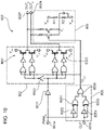
- one or more embodiments may relate to a transmitter circuit 802' (possibly formed in a low voltage die 80a of an otherwise conventional isolated driver device 10) as exemplified in the circuit block diagram of Figure 8 .
- the transmitter circuit 802' comprises an input pin 801a configured to receive a single ended pulse-width modulated input signal PWM IN , and an input pin 801b configured to receive a clock signal CLK having a frequency higher than the frequency of the input signal PWM IN .
- the frequency of the input signal PWM IN may be in the range of 15 kHz to 5 MHz.
- the frequency of the clock signal CLK may be from 2 times higher to 100 times higher than the frequency of the input signal PWM IN ; optionally, the frequency of the clock signal CLK may be about 50 times higher than the frequency of the input signal PWM IN .
- the frequency of the clock signal CLK may be in the range of 8 MHz to 40 MHz; optionally, the frequency of the clock signal CLK may be about 10 MHz.
- the signals PWM IN and CLK may be received from an external circuit, e.g., a microcontroller not visible in the Figures annexed herein.
- the transmitter circuit 802' comprises a tri-state transmitter 802 coupled to the input pin 801a and configured to convert the received single ended signal PWM IN into a pair of differential pulse-width modulated signals OUT P ,OUT N .
- signal OUT P may be generated at the output of a buffer circuit 8021 that receives the input signal PWM IN at input
- signal OUT N may be generated at the output of another buffer circuit 8023 that receives an inverted replica (e.g., via inverter 8022) of the input signal PWM IN at input.
- the die 80a comprises a first high voltage capacitance 803P (e.g., an isolation capacitance) having a first terminal coupled to the first output of the tri-state transmitter 802 (e.g., coupled to the output node 802P of buffer 8021) to receive signal OUT P , and a second high voltage capacitance 803N (e.g., an isolation capacitance) having a first terminal coupled to the second output of the tri-state transmitter 802 (e.g., coupled to the output node 802N of buffer 8023) to receive signal OUT N .
- a first high voltage capacitance 803P e.g., an isolation capacitance
- 803N e.g., an isolation capacitance
- the second terminals of the capacitances 803P, 803N provide the output nodes 804P, 804N of the low voltage die 80a, which can be connected (e.g., via bonding wires) to the input nodes of a high voltage die (e.g., including a receiver circuit), in a configuration as exemplified in Figure 1 .
- the signals OUT P , OUT N are filtered by the isolation capacitances 803P, 803N so that a differential signal V d is produced at the output nodes 804P, 804N.
- the output buffers 8021, 8023 of the tri-state transmitter 802 have three possible output states.
- a pull-up path e.g., a pull-up transistor
- the output node of the buffer is forced to a high value, such as a power supply voltage level V DD .
- a pull-down path e.g., a pull-down transistor
- the output node of the buffer is forced to a low value, such as a negative or reference voltage level Vss.
- both the pull-up path and the pull-down path are inactive (e.g., non conductive or off) and the output node of the buffer can be driven externally.
- the transmitter circuit 802' comprises a logic circuit 805 configured to receive signals PWM IN and CLK.
- the logic circuit 805 is configured to produce a control signal TX DIS that is propagated to the tri-state transmitter 802 to control the operating state of buffers 8021, 8023.
- the control signal TX DIS may be generated by the logic circuit 805 as a pulsed signal that normally has a first value (e.g., a high logic value) and switches to a second value (e.g., a low logic value) for a short time T HIZ each time that an edge (e.g., both rising and falling edges) is detected in the clock signal CLK or in the input signal PWM IN .
- the time interval T HIZ may be in the range of 0.2 ⁇ T CLK to 0.25 ⁇ T CLK (T CLK being the period of the clock signal CLK ).
- T CLK being the period of the clock signal CLK
- the time interval T HIZ may be in the range of 8 ns to 12 ns; optionally, the time interval T HIZ may be about 10 ns.
- the buffers 8021, 8023 may be forced to the high impedance state when the control signal TX DIS has the first value (e.g., high).
- the transmitter circuit 802' comprises an output control circuit 806 configured to receive the control signal TX DIS and configured to drive the output nodes 802P and 802N of buffers 8021 and 8023 (i.e., signals OUT P and OUT N ) when the buffers 8021 and 8023 are in the high impedance state.
- the output control circuit 806 is configured to force signals OUT P and OUT N , during the high impedance state of buffers 8021 and 8023 (e.g., when the control signal TX DIS has the first value), to a voltage V X that is intermediate between the minimum and maximum values of signals OUT P and OUT N (e.g., at the center of the swing range of signals OUT P and OUT N ).
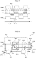
- FIG. 8 Operation of a transmitter circuit 802' as exemplified in Figure 8 can be further understood with reference to Figure 9 , which illustrates exemplary time diagrams of signals PWM IN , CLK, TX DIS , OUT P , OUT N and V d as possibly received and produced in the transmitter circuit 802' and low voltage die 80a.
- Figure 9 illustrates exemplary time diagrams of signals PWM IN , CLK, TX DIS , OUT P , OUT N and V d as possibly received and produced in the transmitter circuit 802' and low voltage die 80a.
- control signal TX DIS may be normally set to a high logic value ('1').
- the tri-state transmitter 802 is in the high impedance state (i.e., both buffers 8021 and 8023 are in the high impedance state) and the signals OUT P and OUT N are forced to value Vx by the output control circuit 806.
- the control signal TX DIS is set by the logic circuit 805 to a low logic value ('0') for a short period of time T HIZ .
- the tri-state transmitter 802 operates normally, i.e., signals OUT P and OUT N are driven by buffers 8021 and 8023 as a function of the value of the input signal PWM IN (e.g., with signal OUT P having the same polarity as signal PWM IN , and signal OUT N having the opposite polarity of signal PWM IN ).
- the transition from the high impedance state to the active states (high or low) of the buffers 8021 and 8023 is fast.
- signals OUT P and OUT N are sharp (e.g., may have a duration in the range of 10 ps to 100 ps). Since signals OUT P and OUT N are filtered by the capacitances 803P and 803N, corresponding pulses are produced in the differential signal V d , as exemplified in Figure 9 .
- the control signal TX DIS After a time interval T HIZ (determined by the logic circuit 805), the control signal TX DIS returns to its normal value (e.g., high in the example considered herein), so that the tri-state transmitter 802 returns in the high impedance state and signals OUT P and OUT N are again forced to value V x by the output control circuit 806.
- the transitions of signals OUT P and OUT N from the extreme values (minimum or maximum) to the intermediate value Vx are slow (e.g., may have a duration in the range of 30 ns to 40 ns, or generally some orders of magnitude higher than the duration of the transitions from the intermediate value Vx to the extreme values). Since signals OUT P and OUT N are filtered by the capacitances 803P and 803N, no pulses (or negligible pulses) are produced in the differential signal V d , as exemplified in Figure 9 .
- Figure 10 is a circuit diagram exemplary of a possible implementation of a transmitter circuit 802' according to one or more embodiments.
- Figure 10 is exemplary of possible implementation details of the logic circuit 805, the tri-state transmitter 802 and the output control circuit 806.
- the logic circuit 805 may comprise a first XOR gate 8051 configured to receive the input signal PWM IN and a delayed replica of the input signal PWM IN (e.g., delayed by means of an interposed buffer stage 8052).
- the logic circuit 805 may comprise a second XOR gate 8053 configured to receive the clock signal CLK and a delayed replica of the clock signal CLK (e.g., delayed by means of an interposed buffer stage 8054). Therefore, the signal produced by the XOR gate 8051 is set to a high logic value at each commutation (edge) of signal PWM IN , and maintains the high logic value (only) for a (short) time period T HIZ equal to the delay of the buffer stage 8052.
- the signal produced by the XOR gate 8053 is set to a high logic value at each commutation (edge) of signal CLK, and maintains the high logic value (only) for a (short) time period T HIZ equal to the delay of the buffer stage 8054.
- the delays of the buffer stages 8052 and 8054 may be equal.
- the logic circuit 805 may comprise a NOR gate 8055 configured to receive the signals produced by the XOR gates 8051 and 8053, thereby producing the control signal TX DIS that is normally high and goes to low for a (short) time period T HIZ at each commutation (edge) of signal PWM IN or signal CLK, as discussed with reference to Figure 9 .
- the tri-state transmitter circuit 802 may comprise a first buffer stage 8021 and a second buffer stage 8023.
- the first buffer stage 8021 may comprise a half-bridge circuit connected between a positive supply voltage node V DD and a negative or reference supply voltage node Vss.
- the half-bridge circuit may comprise a high-side transistor (e.g., p-channel MOS transistor) and a low-side transistor (e.g., n-channel MOS transistor).
- a node 802P intermediate the high-side transistor and the low-side transistor may be configured to produce the signal OUT P .
- the high-side transistor may be controlled by a respective control signal produced by an OR gate that receives signal TX DIS and an inverted replica of signal PWM IN as input signals.
- a buffer or delay stage may be coupled between the output of the OR gate and the control terminal of the high-side transistor.
- the low-side transistor may be controlled by a respective control signal produced by an AND gate that receives an inverted replica of signal TX DIS and an inverted replica of signal PWM IN as input signals.
- the second buffer stage 8023 may comprise a half-bridge circuit connected between the positive supply voltage node V DD and the negative or reference supply voltage node Vss.
- the half-bridge circuit may comprise a high-side transistor (e.g., p-channel MOS transistor) and a low-side transistor (e.g., n-channel MOS transistor).
- a node 802N intermediate the high-side transistor and the low-side transistor may be configured to produce the signal OUT N .
- the high-side transistor may be controlled by a respective control signal produced by an OR gate that receives signal TX DIS and signal PWM IN as input signals.
- a buffer or delay stage may be coupled between the output of the OR gate and the control terminal of the high-side transistor.
- the low-side transistor may be controlled by a respective control signal produced by an AND gate that receives an inverted replica of signal TX DIS and signal PWM IN as input signals.
- signal PWM IN may be slightly delayed (e.g., by a buffer stage 8011) before being propagated to the logic gates which drive the buffers 8021 and 8023.
- the output control circuit 806 may comprise a (e.g., resistive) voltage divider arranged between the positive supply voltage node V DD and the negative or reference supply voltage node Vss.
- the voltage divider may comprise a series arrangement of two resistors R1 and R2; a node intermediate resistors R1 and R2 may produce the intermediate voltage level Vx.
- resistors R1 and R2 may have the same resistance value, so that Vx is centered with respect to the supply rail V DD to Vss.
- the node intermediate resistors R1 and R2 may be selectively connected to the output nodes 802P and 802N of the buffer stages 8021 and 8023 by means of respective switches controlled by the control signal TX DIS .
- a capacitance may be coupled in parallel to the resistor R2 between the intermediate node of the voltage divider and the negative or reference supply voltage node Vss.
- one or more embodiments as exemplified in Figure 11 may additionally comprise a protection circuit 807.
- the protection circuit 807 may comprise a first capacitance C P and a second capacitance C N that are selectively couplable (e.g., by means of respective switches controlled by signal TX DIS ) to the nodes 802P and 802N, respectively.
- TX DIS 0 (active transmission of the tri-state transmitter 802)
- the capacitances C P , C N are decoupled from the nodes 802P, 802N and are charged to V DD or V SS according to the value of the input signal PWM IN .
- TX DIS 1 (high impedance state of the tri-state transmitter 802)
- the capacitances C P and C N are coupled to nodes 802P and 802N, respectively. Therefore, if a common mode pulse occurs in the signals OUT P , OUT N , the capacitances C P , C N can absorb the current avoiding the generation of a spurious transition.
- Figure 11 is a circuit diagram exemplary of a possible implementation of a transmitter circuit 802' according to one or more embodiments.
- Figure 11 is exemplary of possible implementation details of the protection circuit 807.
- the protection circuit 807 may comprise a first capacitance C P coupled to the output node of a respective half-bridge circuit connected between the positive supply voltage node V DD and the negative or reference supply voltage node Vss.
- the half-bridge circuit may comprise a high-side transistor (e.g., p-channel MOS transistor) and a low-side transistor (e.g., n-channel MOS transistor).
- the protection circuit 807 may comprise a second capacitance C N coupled to the output node of a respective half-bridge circuit connected between the positive supply voltage node V DD and the negative or reference supply voltage node Vss.
- the half-bridge circuit may comprise a high-side transistor (e.g., p-channel MOS transistor) and a low-side transistor (e.g., n-channel MOS transistor).
- CMTI common mode transient immunity
- Figure 12 is exemplary of a comparison between signals in an isolated driver device according to one or more embodiments (signals in portion A of Figure 12 ), and signals in an isolated driver device based on OOK modulation (portion B of Figure 12 ).
- the reaction times e.g., the time needed for "correcting" a missed pulse MP12 in the receiver high voltage die 10b
- T react_OOK and T react_retry are comparable.
- signal PWM RX does not suffer from a decoding delay T decoding .
- control signal TX DIS is generated as a function of the edges detected in both signals PWM IN and CLK.
- the frequency of signal CLK being higher than the frequency of signal PWM IN , and considering that the edges of signal PWM IN may be coincident with certain edges of signal CLK (as exemplified in Figure 9 ), one or more embodiments may generate the control signal TX DIS as a function of the edges detected in signal CLK only, without affecting the operating principle of the embodiments.
- the logic circuit 805 may include (only) the XOR gate 8053 and the delay stage 8054, and may include an inverter coupled to the output of the XOR gate 8053 to generate signal TX DIS , in the place of the NOR gate 8055.
- the logic circuit 805 may include (only) the XOR gate 8053 and the delay stage 8054, and may include an inverter coupled to the output of the XOR gate 8053 to generate signal TX DIS , in the place of the NOR gate 8055.
- such simpler embodiments may be effective in applications where the frequency of the input PWM signal PWM IN is much lower than the frequency of the clock signal CLK.
- detecting edges in both signals PWM IN and CLK may improve the robustness of the transmission.
Landscapes
- Engineering & Computer Science (AREA)
- Computer Networks & Wireless Communication (AREA)
- Signal Processing (AREA)
- Physics & Mathematics (AREA)
- Computer Hardware Design (AREA)
- Computing Systems (AREA)
- General Engineering & Computer Science (AREA)
- Mathematical Physics (AREA)
- Power Engineering (AREA)
- Spectroscopy & Molecular Physics (AREA)
- Dc Digital Transmission (AREA)
Abstract
Description
- The description relates to transmitter circuits, e.g., for use in isolated gate driver devices.
- Isolated gate driver devices may be applied, for instance, in traction inverters, DC/DC converters, on-board chargers (OBC), and belt starter generators (BSG) for electric vehicles (EV) and hybrid electric vehicles (HEV).
- Conventional isolated gate driver devices comprise two semiconductor dies arranged in the same package: a low voltage die that usually exchanges signals with a microcontroller, and a high voltage die that includes the driver circuit. The low voltage die and the high voltage die are electrically isolated one from the other by a galvanic isolation barrier, which usually includes one or more high voltage capacitances (HVCap) arranged between the two dies.
-
Figure 1 is a circuit block diagram exemplary of an isolated gate driver device.Figures 2 and 3 are time diagrams of signals in the isolated gate driver device ofFigure 1 , which are exemplary of possible operation of the gate driver device. - As exemplified in
Figure 1 , the isolatedgate driver device 10 comprises alow voltage die 10a and ahigh voltage die 10b in the same package. Thegate driver device 10 comprises aninput pin 101 configured to receive a single ended pulse-width modulated input signal PWMIN (e.g., from a microcontroller, not visible inFigure 1 ). The frequency of the input signal PWMIN may be, for instance, in the range of 15 kHz to 5 MHz. Thelow voltage die 10a comprises atransmitter circuit 102 coupled to theinput pin 101 and configured to convert the received single ended signal PWMIN into a pair of differential pulse-width modulated signals OUTP, OUTN. For instance, signal OUTP may be generated at the output of a buffer circuit that receives the input signal PWMIN at input, and signal OUTN may be generated at the output of another buffer circuit that receives an inverted replica of the input signal PWMIN at input. The low voltage die 10a further comprises a firsthigh voltage capacitance 103P (e.g., an isolation capacitance) having a first terminal coupled to the first output of thetransmitter circuit 102 to receive signal OUTP,and a secondhigh voltage capacitance 103N (e.g., an isolation capacitance) having a first terminal coupled to the second output of thetransmitter circuit 102 to receive signal OUTN. The second terminals of thecapacitances low voltage die 10a, which are connected (e.g., via bonding wires) to the input nodes of thehigh voltage die 10b. The signals OUTP,OUTN are filtered by theisolation capacitances high voltage die 10b. The differential signal Vd comprises a train of pulses (positive and negative) corresponding to the edges (rising and falling, respectively) of the input PWM signal PWMIN, as exemplified inFigure 2 . Thehigh voltage die 10b comprises areceiver circuit 104 coupled to the input nodes of thedie 10b to receive the differential signal Vd, and configured to produce a reconstructed pulse-width modulated signal PWMRX as a function of the received differential signal Vd. For instance, thereceiver circuit 104 may be configured to set the signal PWMRX to a high logic value ('1') as a result of a positive pulse being detected in the differential signal Vd, and to a low logic value ('0') as a result of a negative pulse being detected in the differential signal Vd, as exemplified inFigure 2 . Therefore, the reconstructed signal PWMRX may substantially correspond to a (slightly) delayed copy of the transmitted signal PWMIN, as exemplified inFigure 2 . Thehigh voltage die 10b comprises adriver stage 105 including a pre-driver circuit (e.g.,buffers inverter 1051 and/or amplifying atbuffers gate driver device 10. A node intermediate the high-side transistor and the low-side transistor may be electrically coupled to anoutput pin 106 of thegate driver device 10. The high-side transistor and the low-side transistor are driven by thepre-driver circuit - In various applications, a gate driver device as exemplified in
Figure 1 may be placed (e.g., operated) in a noisy environment. Therefore, for some unpredictable and/or unforeseen reason (e.g., disturbances, interferences, spurious spikes, etc.), one or more pulses in the differential signal Vd may occasionally not be decoded (e.g., detected) by thereceiver circuit 104, as exemplified in the time diagrams ofFigure 3 , where a negative pulse MP3 of signal Vd is not detected by thereceiver circuit 104. In such cases, the reconstructed signal PWMRX may not switch to the expected value and may retain its last value (as exemplified by signal PWMRX that remains stationary at a high logic value at instant tM , when it should switch to a low logic value instead). The reconstructed signal PWMRX switches again at the next "useful" edge correctly detected (e.g., the next falling edge DP3, as exemplified inFigure 3 , if the missed edge was a falling one). In other cases, to the contrary, unexpected spikes (e.g., due to disturbances) in the differential signal Vd may generate spurious, unwanted commutations of the reconstructed signal PWMRX. - In order to mitigate the above-discussed issue (i.e., the issue of missing "good" pulses and/or detecting "spurious" pulses in the signal Vd at the input of the
high voltage die 10b), a conventional approach may rely on using on-off keying (OOK) modulation of the input signal PWMIN, as exemplified inFigures 4, 5 and 6 . In this case, thelow voltage die 10a of thegate driver device 10 comprises amixer circuit 40 that receives the input signal PWMIN(t) and a high frequency carrier signal C(t) (e.g., a sinusoidal signal having a frequency in the range of 100 MHz to 500 MHz) and produces an OOK-modulated signal PWMTX(t) for transmission to thetransmitter circuit 102, according to the known equations of OOK modulation, reproduced in the following:

- Additionally, the
low voltage die 10a of thegate driver device 10 may comprise an oscillator circuit for generating the high frequency carrier signal C(t). - According to this approach, the
receiver circuit 104 may be configured to count a number N of pulses (e.g., N=2 as exemplified inFigures 5 and 6 ) to reconstruct the PWM signal PWMRX. After receiving a number N of pulses, thereceiver circuit 104 asserts (e.g., sets to a high logic value) the reconstructed signal PWMRX. Otherwise, the reconstructed signal PWMRX remains de-asserted (e.g., set to a low logic value). If thereceiver circuit 104 misses a pulse, it may still be able to reconstruct the signal PWMRX, insofar as it will start counting the pulses from the pulse that immediately follows the missed one: see, for instance, the missed pulse MP6 inFigure 6 , with the output signal PWMRX(t) being asserted (e.g., set to a high logic value) at the third pulse of signal PWMTX(t), because thereceiver circuit 104 started counting on the second pulse instead of the first one. The higher is the frequency of the carrier signal C(t), the faster is the receiver circuit in correcting the value of the reconstructed signal PWMRX. - However, an approach based on OOK modulation introduces a delay in the communication between the
low voltage die 10a and thehigh voltage die 10b, insofar as thereceiver circuit 104 needs a time interval Tdecoding before assigning the right value to the reconstructed signal PWMRX at each commutation thereof, as exemplified inFigures 5 and 6 . The time interval Tdecoding is substantially equal to N times the period of the carrier signal C(t), N being again the number of pulses detected (e.g., counted) before assigning a new value (e.g., asserting and/or deasserting) to the signal PWMRX(t). - Therefore, there is a need in the art to provide improved transmitter circuits (e.g., for use in isolated gate driver devices) that facilitate mitigating the issue discussed above without the disadvantages of the known solutions.
- An object of one or more embodiments is to contribute in providing such improved transmitter circuits.
- According to one or more embodiments, such an object can be achieved by means of a circuit having the features set forth in the claims that follow.
- One or more embodiments may relate to a corresponding isolated driver device.
- One or more embodiments may relate to a corresponding electronic system.
- One or more embodiments may relate to a corresponding method of encoding a pulse-width modulated signal into a differential pulsed signal.
- The claims are an integral part of the technical teaching provided herein in respect of the embodiments.
- In one or more embodiments, a circuit comprises a first input node configured to receive a pulse-width modulated input signal, and a second input node configured to receive a clock signal having a frequency higher than the frequency of the pulse-width modulated input signal. The circuit comprises a logic circuit sensitive to the clock signal and configured to generate a control signal as a function of the clock signal. The control signal is normally set to a first logic value (e.g., high), and is periodically set to a second logic value (e.g., low) for a transmission time interval in response to an edge being detected in the clock signal. The transmission time interval is shorter than half clock period of the clock signal. The circuit comprises a tri-state transmitter coupled to the first input node to receive the pulse-width modulated input signal and sensitive to the control signal. The tri-state transmitter is configured to produce a first output signal at a first transmitter output node and a second output signal at a second transmitter output node. The first output signal and the second output signal have a voltage swing between a positive supply voltage and a reference supply voltage. The circuit comprises an output control circuit sensitive to the control signal and coupled to the first transmitter output node and the second transmitter output node. In response to the control signal having the first logic value, the tri-state transmitter sets the first transmitter output node and the second transmitter output node to a high impedance state, and the output control circuit drives the first transmitter output node and the second transmitter output node to an intermediate voltage level between the positive supply voltage and the reference supply voltage. In response to the control signal having the second logic value, the tri-state transmitter drives the first transmitter output node to the positive supply voltage or to the reference supply voltage according to the logic value of the pulse-width modulated input signal, and drives the second transmitter output node to the positive supply voltage or to the reference supply voltage according to the inverted logic value of the pulse-width modulated input signal. The tri-state transmitter is faster than the output control circuit in driving the first transmitter output node and the second transmitter output node.
- One or more embodiments may thus facilitate providing a transmitter circuit for use in an isolated driver device which is robust against noise and does not introduce delay in the signal transmission path, while also having a simple circuit architecture.
- In one or more embodiments, the tri-state transmitter may drive the first transmitter output node and the second transmitter output node to the positive supply voltage and to the reference supply voltage with a respective transition time that is at least 100 times shorter than the transition time with which the output control circuit drives the first transmitter output node and the second transmitter output node to the intermediate voltage level.
- In one or more embodiments, the tri-state transmitter may drive the first transmitter output node and the second transmitter output node to the positive supply voltage and to the reference supply voltage with a respective transition time in the range of 10 ps to 100 ps, and the output control circuit may drive the first transmitter output node and the second transmitter output node to the intermediate voltage level with a respective transition time in the range of 30 ns to 40 ns.
- In one or more embodiments, the logic circuit may comprise a first delay circuit element configured to produce a delayed replica of the clock signal; a first XOR gate configured to receive the clock signal and the delayed replica of the clock signal as input; and an inverter circuit configured to invert the output signal from the first XOR gate to produce the control signal. The transmission time interval may be equal to the delay generated by the first delay circuit element.
- In one or more embodiments, the logic circuit may be further sensitive to the pulse-width modulated input signal and may be configured to generate the control signal further as a function of the pulse-width modulated input signal. The control signal may be set to the second logic value for the transmission time interval is in response to an edge being detected in the pulse-width modulated input signal.
- In one or more embodiments, the logic circuit may comprise a first delay circuit element configured to produce a delayed replica of the clock signal; a first XOR gate configured to receive the clock signal and the delayed replica of the clock signal as input; a second delay circuit element configured to produce a delayed replica of the pulse-width modulated input signal; a second XOR gate configured to receive the pulse-width modulated input signal and the delayed replica of the pulse-width modulated input signal as input; and a NOR gate configured to receive the output signals from the first XOR gate and the second XOR gate to produce the control signal. The transmission time interval may be equal to the delay generated by the first delay circuit element and by the second delay circuit element.
- In one or more embodiments, the tri-state transmitter may comprise a first half-bridge circuit arranged between the positive supply voltage and the reference supply voltage and having an intermediate node coupled to the first transmitter output node; and a second half-bridge circuit arranged between the positive supply voltage and the reference supply voltage and having an intermediate node coupled to the second transmitter output node. A high-side switch of the first half-bridge circuit may be conductive in response to the control signal having the second logic value and the pulse-width modulated input signal having a high logic value. A low-side switch of the first half-bridge circuit may be conductive in response to the control signal having the second logic value and the pulse-width modulated input signal having a low logic value. A high-side switch of the second half-bridge circuit may be conductive in response to the control signal having the second logic value and the pulse-width modulated input signal having a low logic value. A low-side switch of the second half-bridge circuit may be conductive in response to the control signal having the second logic value and the pulse-width modulated input signal having a high logic value. The high-side switch and the low-side switch of the first half-bridge circuit, as well as the high-side switch and the low-side switch of the second half-bridge circuit, may be non-conductive in response to the control signal having the first logic value.
- In one or more embodiments, the output control circuit may comprise a voltage divider arranged between the positive supply voltage and the reference supply voltage; and respective switches configured to selectively couple an intermediate node of the voltage divider to the first transmitter output node and to the second transmitter output node in response to the control signal having the first logic value.
- In one or more embodiments, the circuit may comprise a protection circuit. The protection circuit may comprise a first protection capacitance, a second protection capacitance, and protection circuitry. The protection circuitry may be configured to charge the first protection capacitance to the positive supply voltage in response to the control signal having the second logic value and the pulse-width modulated input signal having a high logic value; and charge the first protection capacitance to the reference supply voltage in response to the control signal having the second logic value and the pulse-width modulated input signal having a low logic value. The protection circuitry may be configured to charge the second protection capacitance to the positive supply voltage in response to the control signal having the second logic value and the pulse-width modulated input signal having a low logic value; and charge the second protection capacitance to the reference supply voltage in response to the control signal having the second logic value and the pulse-width modulated input signal having a high logic value. The protection circuitry may be configured to couple the first protection capacitance to the first transmitter output node and couple the second protection capacitance to the second transmitter output node in response to the control signal having the first logic value.
- In one or more embodiments, the circuit may comprise a first differential output node and a second differential output node; a first isolation capacitance coupled between the first transmitter output node and the first differential output node; and a second isolation capacitance coupled between the second transmitter output node and the second differential output node. A differential output signal indicative of the pulse-width modulated input signal may be produced between the first differential output node and the second differential output node.
- In one or more embodiments, an isolated driver device may comprise a first semiconductor die having a transmitter circuit according to one or more embodiments implemented thereon; and a second semiconductor die having a first receiver input node and a second receiver input node. The first receiver input node may be electrically coupled to the first differential output node of the transmitter circuit and the second receiver input node may be electrically coupled to the second differential output node of the transmitter circuit to receive the differential output signal. The second semiconductor die may have a receiver circuit implemented thereon. The receiver circuit may be configured to receive the differential output signal, and to set a driving signal to a first logic value in response to a positive pulse being detected in the differential output signal and to a second logic value in response to a negative pulse being detected in the differential output signal.
- In one or more embodiments, the second semiconductor die may have a driver circuit implemented thereon. The driver circuit may include a half-bridge circuit arranged between a positive supply voltage pin and a reference supply voltage pin and driven by the driving signal to produce an output switching signal.
- In one or more embodiments, an electronic system may comprise a processing unit configured to generate the pulse-width modulated input signal and the clock signal; and an isolated driver device according to one or more embodiments, the isolated driver device being coupled to the processing unit to receive the pulse-width modulated input signal and the clock signal.
- In one or more embodiments, a method of encoding a pulse-width modulated signal into a differential pulsed signal comprises receiving the pulse-width modulated signal; providing a clock signal having a frequency higher than the frequency of the pulse-width modulated signal; and generating a control signal as a function of the clock signal. The control signal is normally set to a first logic value, and is periodically set to a second logic value for a transmission time interval in response to an edge being detected in the clock signal. The transmission time interval is shorter than half clock period of the clock signal. The method further comprises producing a first output signal and a second output signal, the first output signal and the second output signal having a voltage swing between a positive supply voltage and a reference supply voltage; and applying capacitive filtering to the first output signal and the second output signal to produce respective first and second filtered output signals, wherein the differential pulsed signal is produced as a difference between the first filtered output signal and the second filtered output signal. Producing the first output signal and the second output signal comprises setting the first output signal and the second output signal to an intermediate voltage level between the positive supply voltage and the reference supply voltage, in response to the control signal having the first logic value. Producing the first output signal and the second output signal comprises setting the first output signal to the positive supply voltage or to the reference supply voltage according to the logic value of the pulse-width modulated input signal, and setting the second output signal to the positive supply voltage or to the reference supply voltage according to the inverted logic value of the pulse-width modulated input signal, in response to the control signal having the second logic value. A time interval for setting the first output signal and the second output signal to the positive supply voltage or to the reference supply voltage is shorter than a time interval for setting the first output signal and the second output signal to the intermediate voltage level.
- One or more embodiments will now be described, by way of example only, with reference to the annexed figures, wherein:
-
Figures 1 to 6 have already been described in the foregoing; -
Figure 7 is exemplary of time diagrams of signals in one or more embodiments of the present description; -
Figure 8 is a circuit block diagram exemplary of a transmitter circuit according to one or more embodiments of the present description; -
Figure 9 is exemplary of time diagrams of signals in one or more embodiments of the present description; -
Figures 10 and11 are circuit diagrams exemplary of implementation details of transmitter circuits according to one or more embodiments of the present description; and -
Figure 12 is exemplary of a comparison between time diagrams of signals in one or more embodiments of the present description and time diagrams of signals in a transmitter circuit based on on-off keying modulation. - In the ensuing description, one or more specific details are illustrated, aimed at providing an in-depth understanding of examples of embodiments of this description. The embodiments may be obtained without one or more of the specific details, or with other methods, components, materials, etc. In other cases, known structures, materials, or operations are not illustrated or described in detail so that certain aspects of embodiments will not be obscured.
- Reference to "an embodiment" or "one embodiment" in the framework of the present description is intended to indicate that a particular configuration, structure, or characteristic described in relation to the embodiment is comprised in at least one embodiment. Hence, phrases such as "in an embodiment" or "in one embodiment" that may be present in one or more points of the present description do not necessarily refer to one and the same embodiment. Moreover, particular configurations, structures, or characteristics may be combined in any adequate way in one or more embodiments.
- The headings/references used herein are provided merely for convenience and hence do not define the extent of protection or the scope of the embodiments.
- Throughout the figures annexed herein, unless the context indicates otherwise, like parts or elements are indicated with like references/numerals and a corresponding description will not be repeated for the sake of brevity.
- One or more embodiments may provide an improved transmitter circuit for use in an isolated driver device, based on the recognition that a receiver circuit in the high voltage die of the driver device may be configured to generate a reconstructed PWM signal PWMRX by setting the signal PWMRX to a high logic value ('1') in response to a positive pulse being detected in the input differential signal Vd, and setting the signal PWMRX to a low logic value ('0') in response to a negative pulse being detected in the input differential signal Vd, as previously discussed with reference to
Figures 1 to 3 . - Therefore, one or more embodiments may rely on the operating principle exemplified in the time diagrams of
Figure 7 and discussed in the following. In one or more embodiments, a transmitter circuit may comprise circuitry configured to convert the received single ended signal PWMIN into a pair of differential pulse-width modulated signals OUTP , OUTN that comprise continuous trains of pulses (e.g., a respective train of pulses for each commutation of the input signal PWMIN). The pulses are generated continuously by resorting to a clock signal CLK having a frequency higher than the frequency of signal PWMIN, so that even if a pulse is lost, the signal PWMRX (reconstructed at the receiver side) can switch correctly at the next pulse. Therefore, in one or more embodiments a transmitter circuit may be configured to generate a pair of signals OUTP and OUTN that, once filtered by thecapacitances Figure 7 , the differential signal Vd may include a positive pulse at each edge (rising or falling) of signals PWMIN and CLK when PWMIN has a high logic value, and a negative pulse at each edge (rising or falling) of signals PWMIN and CLK when PWMIN has a low logic value. According to this operating principle, thereceiver circuit 104 in the high voltage die 10b of the isolated driver device may be able to "correct" the value of the reconstructed signal PWMRX, in the case of a missed pulse and/or spurious pulse, with a delay (e.g., maximum delay) of half clock period. The time diagrams ofFigure 7 illustrate an exemplary case where a pulse MP7 is missed by the receiver circuit at instant tM7 , and the reconstructed signal PWMRX is assigned the correct value (high, in the case exemplified herein) at instant tC7, after a time interval equal to TCLK/2. - Therefore, one or more embodiments may relate to a transmitter circuit 802' (possibly formed in a low voltage die 80a of an otherwise conventional isolated driver device 10) as exemplified in the circuit block diagram of
Figure 8 . - The transmitter circuit 802' comprises an
input pin 801a configured to receive a single ended pulse-width modulated input signal PWMIN, and aninput pin 801b configured to receive a clock signal CLK having a frequency higher than the frequency of the input signal PWMIN. For instance, the frequency of the input signal PWMIN may be in the range of 15 kHz to 5 MHz. The frequency of the clock signal CLK may be from 2 times higher to 100 times higher than the frequency of the input signal PWMIN; optionally, the frequency of the clock signal CLK may be about 50 times higher than the frequency of the input signal PWMIN. For instance, the frequency of the clock signal CLK may be in the range of 8 MHz to 40 MHz; optionally, the frequency of the clock signal CLK may be about 10 MHz. The signals PWMIN and CLK may be received from an external circuit, e.g., a microcontroller not visible in the Figures annexed herein. - The transmitter circuit 802' comprises a
tri-state transmitter 802 coupled to theinput pin 801a and configured to convert the received single ended signal PWMIN into a pair of differential pulse-width modulated signals OUTP,OUTN. For instance, signal OUTP may be generated at the output of abuffer circuit 8021 that receives the input signal PWMIN at input, and signal OUTN may be generated at the output of anotherbuffer circuit 8023 that receives an inverted replica (e.g., via inverter 8022) of the input signal PWMIN at input. Thedie 80a comprises a firsthigh voltage capacitance 803P (e.g., an isolation capacitance) having a first terminal coupled to the first output of the tri-state transmitter 802 (e.g., coupled to theoutput node 802P of buffer 8021) to receive signal OUTP, and a secondhigh voltage capacitance 803N (e.g., an isolation capacitance) having a first terminal coupled to the second output of the tri-state transmitter 802 (e.g., coupled to theoutput node 802N of buffer 8023) to receive signal OUTN. The second terminals of thecapacitances output nodes Figure 1 . The signals OUTP, OUTN are filtered by theisolation capacitances output nodes - The output buffers 8021, 8023 of the
tri-state transmitter 802 have three possible output states. In the "high" output state, a pull-up path (e.g., a pull-up transistor) is active (e.g., conductive) and the output node of the buffer is forced to a high value, such as a power supply voltage level VDD. In the "low" output state, a pull-down path (e.g., a pull-down transistor) is active (e.g., conductive) and the output node of the buffer is forced to a low value, such as a negative or reference voltage level Vss. In the "high impedance" (HIZ) output state, both the pull-up path and the pull-down path are inactive (e.g., non conductive or off) and the output node of the buffer can be driven externally. - The transmitter circuit 802' comprises a
logic circuit 805 configured to receive signals PWMIN and CLK. Thelogic circuit 805 is configured to produce a control signal TXDIS that is propagated to thetri-state transmitter 802 to control the operating state ofbuffers logic circuit 805 as a pulsed signal that normally has a first value (e.g., a high logic value) and switches to a second value (e.g., a low logic value) for a short time THIZ each time that an edge (e.g., both rising and falling edges) is detected in the clock signal CLK or in the input signal PWMIN. For instance, the time interval THIZ may be in the range of 0.2∗TCLK to 0.25∗TCLK (TCLK being the period of the clock signal CLK). For instance, the time interval THIZ may be in the range of 8 ns to 12 ns; optionally, the time interval THIZ may be about 10 ns. Thebuffers - The transmitter circuit 802' comprises an
output control circuit 806 configured to receive the control signal TXDIS and configured to drive theoutput nodes buffers 8021 and 8023 (i.e., signals OUTP and OUTN) when thebuffers output control circuit 806 is configured to force signals OUTP and OUTN, during the high impedance state ofbuffers 8021 and 8023 (e.g., when the control signal TXDIS has the first value), to a voltage VX that is intermediate between the minimum and maximum values of signals OUTP and OUTN (e.g., at the center of the swing range of signals OUTP and OUTN). - Operation of a transmitter circuit 802' as exemplified in
Figure 8 can be further understood with reference toFigure 9 , which illustrates exemplary time diagrams of signals PWMIN, CLK, TXDIS, OUTP, OUTN and Vd as possibly received and produced in the transmitter circuit 802' and low voltage die 80a. - For instance, the control signal TXDIS may be normally set to a high logic value ('1'). As a result of the control signal TXDIS being high, the
tri-state transmitter 802 is in the high impedance state (i.e., bothbuffers output control circuit 806. Each time that an edge (both rising edges and falling edges) occurs in signal CLK or signal PWMIN, the control signal TXDIS is set by thelogic circuit 805 to a low logic value ('0') for a short period of time THIZ. As a result of the control signal TXDIS being low, thetri-state transmitter 802 operates normally, i.e., signals OUTP and OUTN are driven bybuffers buffers capacitances Figure 9 . - After a time interval THIZ (determined by the logic circuit 805), the control signal TXDIS returns to its normal value (e.g., high in the example considered herein), so that the
tri-state transmitter 802 returns in the high impedance state and signals OUTP and OUTN are again forced to value Vx by theoutput control circuit 806. The transitions of signals OUTP and OUTN from the extreme values (minimum or maximum) to the intermediate value Vx are slow (e.g., may have a duration in the range of 30 ns to 40 ns, or generally some orders of magnitude higher than the duration of the transitions from the intermediate value Vx to the extreme values). Since signals OUTP and OUTN are filtered by thecapacitances Figure 9 . -
Figure 10 is a circuit diagram exemplary of a possible implementation of a transmitter circuit 802' according to one or more embodiments. In particular,Figure 10 is exemplary of possible implementation details of thelogic circuit 805, thetri-state transmitter 802 and theoutput control circuit 806. - As exemplified in
Figure 10 , thelogic circuit 805 may comprise afirst XOR gate 8051 configured to receive the input signal PWMIN and a delayed replica of the input signal PWMIN (e.g., delayed by means of an interposed buffer stage 8052). Thelogic circuit 805 may comprise asecond XOR gate 8053 configured to receive the clock signal CLK and a delayed replica of the clock signal CLK (e.g., delayed by means of an interposed buffer stage 8054). Therefore, the signal produced by theXOR gate 8051 is set to a high logic value at each commutation (edge) of signal PWMIN, and maintains the high logic value (only) for a (short) time period THIZ equal to the delay of thebuffer stage 8052. Similarly, the signal produced by theXOR gate 8053 is set to a high logic value at each commutation (edge) of signal CLK, and maintains the high logic value (only) for a (short) time period THIZ equal to the delay of thebuffer stage 8054. The delays of the buffer stages 8052 and 8054 may be equal. Thelogic circuit 805 may comprise a NORgate 8055 configured to receive the signals produced by theXOR gates Figure 9 . - As exemplified in
Figure 10 , thetri-state transmitter circuit 802 may comprise afirst buffer stage 8021 and asecond buffer stage 8023. - The
first buffer stage 8021 may comprise a half-bridge circuit connected between a positive supply voltage node VDD and a negative or reference supply voltage node Vss. The half-bridge circuit may comprise a high-side transistor (e.g., p-channel MOS transistor) and a low-side transistor (e.g., n-channel MOS transistor). Anode 802P intermediate the high-side transistor and the low-side transistor may be configured to produce the signal OUTP. The high-side transistor may be controlled by a respective control signal produced by an OR gate that receives signal TXDIS and an inverted replica of signal PWMIN as input signals. A buffer or delay stage may be coupled between the output of the OR gate and the control terminal of the high-side transistor. Therefore, the high-side transistor may be active (and signal OUTP may be forced to the high value VDD) when TXDIS = 0 and PWMIN = 1. The low-side transistor may be controlled by a respective control signal produced by an AND gate that receives an inverted replica of signal TXDIS and an inverted replica of signal PWMIN as input signals. A buffer or delay stage may be coupled between the output of the AND gate and the control terminal of the low-side transistor. Therefore, the low-side transistor may be active (and signal OUTP may be forced to the low value Vss) when TXDIS = 0 and PWMIN = 0. Both the high-side transistor and the low-side transistor may be inactive (and signal OUTP may be forced to the intermediate value VX under the operation of the output control circuit 806) when TXDIS = 1, irrespective of the value of signal PWMIN. - Similarly, the
second buffer stage 8023 may comprise a half-bridge circuit connected between the positive supply voltage node VDD and the negative or reference supply voltage node Vss. The half-bridge circuit may comprise a high-side transistor (e.g., p-channel MOS transistor) and a low-side transistor (e.g., n-channel MOS transistor). Anode 802N intermediate the high-side transistor and the low-side transistor may be configured to produce the signal OUTN. The high-side transistor may be controlled by a respective control signal produced by an OR gate that receives signal TXDIS and signal PWMIN as input signals. A buffer or delay stage may be coupled between the output of the OR gate and the control terminal of the high-side transistor. Therefore, the high-side transistor may be active (and signal OUTN may be forced to the high value VDD) when TXDIS = 0 and PWMIN = 0. The low-side transistor may be controlled by a respective control signal produced by an AND gate that receives an inverted replica of signal TXDIS and signal PWMIN as input signals. A buffer or delay stage may be coupled between the output of the AND gate and the control terminal of the low-side transistor. Therefore, the low-side transistor may be active (and signal OUTN may be forced to the low value Vss) when TXDIS = 0 and PWMIN = 1. Both the high-side transistor and the low-side transistor may be inactive (and signal OUTN may be forced to the intermediate value Vx under the operation of the output control circuit 806) when TXDIS = 1, irrespective of the value of signal PWMIN. - As exemplified in
Figure 10 , signal PWMIN may be slightly delayed (e.g., by a buffer stage 8011) before being propagated to the logic gates which drive thebuffers - As exemplified in
Figure 10 , theoutput control circuit 806 may comprise a (e.g., resistive) voltage divider arranged between the positive supply voltage node VDD and the negative or reference supply voltage node Vss. For instance, the voltage divider may comprise a series arrangement of two resistors R1 and R2; a node intermediate resistors R1 and R2 may produce the intermediate voltage level Vx. Optionally, resistors R1 and R2 may have the same resistance value, so that Vx is centered with respect to the supply rail VDD to Vss. The node intermediate resistors R1 and R2 may be selectively connected to theoutput nodes tri-state transmitter 802 is in the high impedance state (e.g., when TXDIS = 1). Optionally, a capacitance may be coupled in parallel to the resistor R2 between the intermediate node of the voltage divider and the negative or reference supply voltage node Vss. - It is noted that, when operating in the high impedance state, the transmitter circuit 802' may be vulnerable to common mode transient pulses. Therefore, one or more embodiments as exemplified in
Figure 11 may additionally comprise aprotection circuit 807. Theprotection circuit 807 may comprise a first capacitance CP and a second capacitance CN that are selectively couplable (e.g., by means of respective switches controlled by signal TXDIS) to thenodes nodes nodes -
Figure 11 is a circuit diagram exemplary of a possible implementation of a transmitter circuit 802' according to one or more embodiments. In particular,Figure 11 is exemplary of possible implementation details of theprotection circuit 807. - As exemplified in
Figure 11 , theprotection circuit 807 may comprise a first capacitance CP coupled to the output node of a respective half-bridge circuit connected between the positive supply voltage node VDD and the negative or reference supply voltage node Vss. The half-bridge circuit may comprise a high-side transistor (e.g., p-channel MOS transistor) and a low-side transistor (e.g., n-channel MOS transistor). A node intermediate the high-side transistor and the low-side transistor may be coupled to the capacitance CP, and may be selectively coupled tonode 802P via a switch controlled by signal TXDIS (e.g., set to a conductive state when TXDIS = 1). The high-side transistor may be controlled by a respective control signal produced by an OR gate that receives signal TXDIS and an inverted replica of signal PWMIN as input signals. Therefore, the high-side transistor may be active (and the capacitance CP may be charged to VDD) when TXDIS = 0 and PWMIN = 1. The low-side transistor may be controlled by a respective control signal produced by an AND gate that receives an inverted replica of signal TXDIS and an inverted replica of signal PWMIN as input signals. Therefore, the low-side transistor may be active (and the capacitance CP may be charged to Vss) when TXDIS = 0 and PWMIN = 0. Both the high-side transistor and the low-side transistor may be inactive (and the capacitance CP may be coupled tonode 802P) when TXDIS = 1, irrespective of the value of signal PWMIN. - Similarly, the
protection circuit 807 may comprise a second capacitance CN coupled to the output node of a respective half-bridge circuit connected between the positive supply voltage node VDD and the negative or reference supply voltage node Vss. The half-bridge circuit may comprise a high-side transistor (e.g., p-channel MOS transistor) and a low-side transistor (e.g., n-channel MOS transistor). A node intermediate the high-side transistor and the low-side transistor may be coupled to the capacitance CN, and may be selectively coupled tonode 802N via a switch controlled by signal TXDIS (e.g., set to a conductive state when TXDIS = 1). The high-side transistor may be controlled by a respective control signal produced by an OR gate that receives signal TXDIS and signal PWMIN as input signals. Therefore, the high-side transistor may be active (and the capacitance CN may be charged to VDD) when TXDIS = 0 and PWMIN = 0. The low-side transistor may be controlled by a respective control signal produced by an AND gate that receives an inverted replica of signal TXDIS and signal PWMIN as input signals. Therefore, the low-side transistor may be active (and the capacitance CN may be charged to Vss) when TXDIS = 0 and PWMIN = 1. Both the high-side transistor and the low-side transistor may be inactive (and the capacitance CN may be coupled tonode 802N) when TXDIS = 1, irrespective of the value of signal PWMIN. Therefore, one or more embodiments as exemplified inFigure 11 may provide improved common mode transient immunity (CMTI). -
Figure 12 is exemplary of a comparison between signals in an isolated driver device according to one or more embodiments (signals in portion A ofFigure 12 ), and signals in an isolated driver device based on OOK modulation (portion B ofFigure 12 ). As exemplified inFigure 12 , the reaction times (e.g., the time needed for "correcting" a missed pulse MP12 in the receiverhigh voltage die 10b) Treact_OOK and Treact_retry are comparable. Advantageously, in one or more embodiments (portion A) signal PWMRX does not suffer from a decoding delay Tdecoding. - One or more embodiments have been disclosed herein, where the control signal TXDIS is generated as a function of the edges detected in both signals PWMIN and CLK. However, due to the frequency of signal CLK being higher than the frequency of signal PWMIN, and considering that the edges of signal PWMIN may be coincident with certain edges of signal CLK (as exemplified in
Figure 9 ), one or more embodiments may generate the control signal TXDIS as a function of the edges detected in signal CLK only, without affecting the operating principle of the embodiments. For instance, in one or more embodiments thelogic circuit 805 may include (only) theXOR gate 8053 and thedelay stage 8054, and may include an inverter coupled to the output of theXOR gate 8053 to generate signal TXDIS, in the place of the NORgate 8055. On one hand, such simpler embodiments may be effective in applications where the frequency of the input PWM signal PWMIN is much lower than the frequency of the clock signal CLK. On the other hand, detecting edges in both signals PWMIN and CLK may improve the robustness of the transmission. - One or more embodiments may thus provide one or more of the following advantages:
- possibility of decoding the PWM input signal without delay;
- no need for an oscillator circuit for generating a high frequency carrier signal for modulation; and
- a simple implementation of the receiver circuit.
- Without prejudice to the underlying principles, the details and embodiments may vary, even significantly, with respect to what has been described by way of example only, without departing from the extent of protection.
- The extent of protection is determined by the annexed claims.
Claims (14)
- A circuit (802'), comprising:a first input node (801a) configured to receive a pulse-width modulated input signal (PWMIN );a second input node (801b) configured to receive a clock signal (CLK) having a frequency higher than the frequency of said pulse-width modulated input signal (PWMIN );a logic circuit (805) sensitive to said clock signal (CLK) and configured to generate a control signal (TXDIS ) as a function of said clock signal (CLK), wherein said control signal (TXDIS ) is normally set to a first logic value, and is periodically set to a second logic value for a transmission time interval (THIZ) in response to an edge being detected in said clock signal (CLK), said transmission time interval (THIZ) being shorter than half clock period of said clock signal (CLK);a tri-state transmitter (802) coupled to the first input node (801a) to receive said pulse-width modulated input signal (PWMIN ) and sensitive to said control signal (TXDIS ), the tri-state transmitter (802) being configured to produce a first output signal (OUTP ) at a first transmitter output node (802P) and a second output signal (OUTN ) at a second transmitter output node (802N), the first output signal (OUTP ) and the second output signal (OUTN ) having a voltage swing between a positive supply voltage (VDD ) and a reference supply voltage (Vss);an output control circuit (806) sensitive to said control signal (TXDIS ) and coupled to said first transmitter output node (802P) and said second transmitter output node (802N);wherein:in response to said control signal (TXDIS ) having said first logic value, said tri-state transmitter (802) sets said first transmitter output node (802P) and said second transmitter output node (802N) to a high impedance state, and said output control circuit (806) drives said first transmitter output node (802P) and said second transmitter output node (802N) to an intermediate voltage level (Vx) between said positive supply voltage (VDD ) and said reference supply voltage (Vss ); andin response to said control signal (TXDIS ) having said second logic value, said tri-state transmitter (802) drives said first transmitter output node (802P) to said positive supply voltage (VDD ) or to said reference supply voltage (Vss ) according to the logic value of said pulse-width modulated input signal (PWMIN ), and drives said second transmitter output node (802P) to said positive supply voltage (VDD ) or to said reference supply voltage (Vss ) according to the inverted logic value of said pulse-width modulated input signal (PWMIN ),wherein said tri-state transmitter (802) is faster than said output control circuit (806) in driving said first transmitter output node (802P) and said second transmitter output node (802N).
- The circuit (802') of claim 1, wherein said tri-state transmitter (802) drives said first transmitter output node (802P) and said second transmitter output node (802N) to said positive supply voltage (VDD ) and to said reference supply voltage (Vss ) with a respective transition time that is at least 100 times shorter than the transition time with which said output control circuit (806) drives said first transmitter output node (802P) and said second transmitter output node (802N) to said intermediate voltage level (Vx ).
- The circuit (802') of claim 1 or claim 2, wherein said tri-state transmitter (802) drives said first transmitter output node (802P) and said second transmitter output node (802N) to said positive supply voltage (VDD ) and to said reference supply voltage (Vss ) with a respective transition time in the range of 10 ps to 100 ps, and wherein said output control circuit (806) drives said first transmitter output node (802P) and said second transmitter output node (802N) to said intermediate voltage level (Vx ) with a respective transition time in the range of 30 ns to 40 ns.
- The circuit (802') of any of the previous claims, wherein said logic circuit (805) comprises:a first delay circuit element (8054) configured to produce a delayed replica of said clock signal (CLK);a first XOR gate (8053) configured to receive said clock signal (CLK) and said delayed replica of said clock signal (CLK) as input; andan inverter circuit configured to invert the output signal from said first XOR gate (8053) to produce said control signal (TXDIS ).
- The circuit (802') of any of claims 1 to 3, wherein said logic circuit (805) is further sensitive to said pulse-width modulated input signal (PWMIN ) and is configured to generate said control signal (TXDIS ) further as a function of said pulse-width modulated input signal (PWMIN ), wherein said control signal (TXDIS ) is set to said second logic value for said transmission time interval (THIZ) is in response to an edge being detected in said pulse-width modulated input signal (PWMIN).
- The circuit (802') of claim 5, wherein said logic circuit (805) comprises:a first delay circuit element (8054) configured to produce a delayed replica of said clock signal (CLK);a first XOR gate (8053) configured to receive said clock signal (CLK) and said delayed replica of said clock signal (CLK) as input;a second delay circuit element (8052) configured to produce a delayed replica of said pulse-width modulated input signal (PWMIN );a second XOR gate (8051) configured to receive said pulse-width modulated input signal (PWMIN ) and said delayed replica of said pulse-width modulated input signal (PWMIN ) as input; anda NOR gate (8055) configured to receive the output signals from said first XOR gate (8053) and said second XOR gate (8051) to produce said control signal (TXDIS ).
- The circuit (802') of any of the previous claims, wherein said tri-state transmitter (802) comprises:a first half-bridge circuit (8021) arranged between said positive supply voltage (VDD ) and said reference supply voltage (Vss ) and having an intermediate node coupled to said first transmitter output node (802P); anda second half-bridge circuit (8023) arranged between said positive supply voltage (VDD ) and said reference supply voltage (Vss ) and having an intermediate node coupled to said second transmitter output node (802N);wherein:a high-side switch of said first half-bridge circuit (8021) is conductive in response to said control signal (TXDIS ) having said second logic value and said pulse-width modulated input signal (PWMIN ) having a high logic value;a low-side switch of said first half-bridge circuit (8021) is conductive in response to said control signal (TXDIS ) having said second logic value and said pulse-width modulated input signal (PWMIN ) having a low logic value;a high-side switch of said second half-bridge circuit (8023) is conductive in response to said control signal (TXDIS ) having said second logic value and said pulse-width modulated input signal (PWMIN ) having a low logic value;a low-side switch of said second half-bridge circuit (8023) is conductive in response to said control signal (TXDIS ) having said second logic value and said pulse-width modulated input signal (PWMIN ) having a high logic value; andsaid high-side switch and said low-side switch of said first half-bridge circuit (8021), as well as said high-side switch and said low-side switch of said second half-bridge circuit (8023), are non-conductive in response to said control signal (TXDIS ) having said first logic value.
- The circuit (802') of any of the previous claims, wherein said output control circuit (806) comprises:a voltage divider (R1, R2) arranged between said positive supply voltage (VDD ) and said reference supply voltage (Vss), andrespective switches configured to selectively couple an intermediate node of said voltage divider (R1, R2) to said first transmitter output node (802P) and said second transmitter output node (802N) in response to said control signal (TXDIS ) having said first logic value.
- The circuit (802') of any of the previous claims, comprising a protection circuit (807), wherein the protection circuit (807) comprises a first protection capacitance (CP), a second protection capacitance (CN), and protection circuitry configured to:charge said first protection capacitance (CP) to said positive supply voltage (VDD ) in response to said control signal (TXDIS ) having said second logic value and said pulse-width modulated input signal (PWMIN ) having a high logic value;charge said first protection capacitance (CP) to said reference supply voltage (Vss ) in response to said control signal (TXDIS ) having said second logic value and said pulse-width modulated input signal (PWMIN ) having a low logic value;charge said second protection capacitance (CN) to said positive supply voltage (VDD ) in response to said control signal (TXDIS ) having said second logic value and said pulse-width modulated input signal (PWMIN ) having a low logic value;charge said second protection capacitance (CN) to said reference supply voltage (Vss ) in response to said control signal (TXDIS ) having said second logic value and said pulse-width modulated input signal (PWMIN ) having a high logic value; andcouple said first protection capacitance (CP) to said first transmitter output node (802P) and couple said second protection capacitance (CN) to said second transmitter output node (802N) in response to said control signal (TXDIS ) having said first logic value.
- The circuit (80a) of any of the previous claims, comprising:a first differential output node (804P) and a second differential output node (804N);a first isolation capacitance (803P) coupled between said first transmitter output node (802P) and said first differential output node (804P); anda second isolation capacitance (803N) coupled between said second transmitter output node (802N) and said second differential output node (804N);wherein a differential output signal (Vd ) indicative of said pulse-width modulated input signal (PWMIN ) is produced between said first differential output node (804P) and said second differential output node (804N).
- An isolated driver device, comprising:a first semiconductor die having a transmitter circuit (80a) according to claim 10 implemented thereon;a second semiconductor die having a first receiver input node and a second receiver input node, the first receiver input node being electrically coupled to the first differential output node (804P) of the transmitter circuit (80a) and the second receiver input node being electrically coupled to the second differential output node (804N) of the transmitter circuit (80a) to receive said differential output signal (Vd);wherein the second semiconductor die has a receiver circuit implemented thereon, the receiver circuit being configured to receive said differential output signal (Vd ), and to set a driving signal (PWMRX ) to a first logic value in response to a positive pulse being detected in said differential output signal (Vd ) and to a second logic value in response to a negative pulse being detected in said differential output signal (Vd ).
- The isolated driver device of claim 11, wherein the second semiconductor die has a driver circuit implemented thereon, the driver circuit including a half-bridge circuit arranged between a positive supply voltage pin (VH) and a reference supply voltage pin (VL) and driven by said driving signal (PWMRX ) to produce an output switching signal (OUT).
- An electronic system, comprising a processing unit configured to generate said pulse-width modulated input signal (PWMIN ) and said clock signal (CLK), and an isolated driver device according to claim 11 or claim 12 coupled to the processing unit to receive said pulse-width modulated input signal (PWMIN ) and said clock signal (CLK).
- A method of encoding a pulse-width modulated signal (PWMIN ) into a differential pulsed signal (Vd ), the method comprising:receiving said pulse-width modulated signal (PWMIN );providing a clock signal (CLK) having a frequency higher than the frequency of said pulse-width modulated signal (PWMIN );generating a control signal (TXDIS ) as a function of said clock signal (CLK), wherein said control signal (TXDIS ) is normally set to a first logic value, and is periodically set to a second logic value for a transmission time interval (THIZ) in response to an edge being detected in said clock signal (CLK), said transmission time interval (THIZ) being shorter than half clock period of said clock signal (CLK);producing a first output signal (OUTP ) and a second output signal (OUTN ), the first output signal (OUTP ) and the second output signal (OUTN ) having a voltage swing between a positive supply voltage (VDD ) and a reference supply voltage (Vss ); andapplying capacitive filtering to said first output signal (OUTP ) and said second output signal (OUTN ) to produce respective first and second filtered output signals, wherein said differential pulsed signal (Vd ) is produced as a difference between said first filtered output signal and said second filtered output signal;wherein producing said first output signal (OUTP ) and said second output signal (OUTN ) comprises:in response to said control signal (TXDIS ) having said first logic value, setting said first output signal (OUTP ) and said second output signal (OUTN ) to an intermediate voltage level (Vx) between said positive supply voltage (VDD ) and said reference supply voltage (Vss); andin response to said control signal (TXDIS ) having said second logic value, setting said first output signal (OUTP ) to said positive supply voltage (VDD ) or to said reference supply voltage (Vss ) according to the logic value of said pulse-width modulated input signal (PWMIN ), and setting said second output signal (OUTN ) to said positive supply voltage (VDD ) or to said reference supply voltage (Vss ) according to the inverted logic value of said pulse-width modulated input signal (PWMIN ),wherein a time interval for setting said first output signal (OUTP ) and said second output signal (OUTN ) to said positive supply voltage (VDD ) or to said reference supply voltage (Vss) is shorter than a time interval for setting said first output signal (OUTP) and said second output signal (OUTN) to said intermediate voltage level (Vx).
Applications Claiming Priority (1)
| Application Number | Priority Date | Filing Date | Title |
|---|---|---|---|
| IT202100017000 | 2021-06-29 |
Publications (1)
| Publication Number | Publication Date |
|---|---|
| EP4113845A1 true EP4113845A1 (en) | 2023-01-04 |
Family
ID=77802107
Family Applications (1)
| Application Number | Title | Priority Date | Filing Date |
|---|---|---|---|
| EP22178676.7A Pending EP4113845A1 (en) | 2021-06-29 | 2022-06-13 | Transmitter circuit, corresponding isolated driver device, electronic system and method of encoding a pulse-width modulated signal into a differential pulsed signal |
Country Status (3)
| Country | Link |
|---|---|
| US (1) | US12015515B2 (en) |
| EP (1) | EP4113845A1 (en) |
| CN (1) | CN115549659A (en) |
Cited By (1)
| Publication number | Priority date | Publication date | Assignee | Title |
|---|---|---|---|---|
| WO2025117986A1 (en) * | 2023-12-01 | 2025-06-05 | Microchip Technology Incorporated | Silicon carbide driver using high voltage capacitors for isolation and signal transmission |
Families Citing this family (4)
| Publication number | Priority date | Publication date | Assignee | Title |
|---|---|---|---|---|
| EP4383571A1 (en) | 2022-12-07 | 2024-06-12 | STMicroelectronics International N.V. | Receiver circuit, corresponding isolated driver device, electronic system and method of decoding a differential signal into a digital output signal |
| IT202200026067A1 (en) * | 2022-12-20 | 2024-06-20 | St Microelectronics Int Nv | Receiver circuit, corresponding isolated driver, electronic system and method for decoding a differential signal into a digital output signal |
| US20250183890A1 (en) * | 2023-12-01 | 2025-06-05 | Microchip Technology Incorporated | Silicon Carbide Driver Using High Voltage Capacitors for Isolation and Signal Transmission |
| CN119883989B (en) * | 2025-03-26 | 2025-07-15 | 中茵微电子(南京)有限公司 | Based on LPDDR5/5X PHY IO circuit |
Citations (2)
| Publication number | Priority date | Publication date | Assignee | Title |
|---|---|---|---|---|
| US20060279354A1 (en) * | 2005-06-13 | 2006-12-14 | Texas Instruments, Inc. | Reduction of audible artifacts in an audio system |
| WO2020011801A1 (en) * | 2018-07-10 | 2020-01-16 | Vddtech | Digital isolator |
Family Cites Families (7)
| Publication number | Priority date | Publication date | Assignee | Title |
|---|---|---|---|---|
| US6167132A (en) * | 1997-04-22 | 2000-12-26 | Silicon Laboratories, Inc. | Analog successive approximation (SAR) analog-to-digital converter (ADC) |
| US9998301B2 (en) * | 2014-11-03 | 2018-06-12 | Analog Devices, Inc. | Signal isolator system with protection for common mode transients |
| US10763844B2 (en) * | 2018-08-28 | 2020-09-01 | Texas Instruments Incorporated | Methods and apparatus to transmit signals in isolated gate drivers |
| US10797608B2 (en) * | 2019-02-14 | 2020-10-06 | Dialog Semiconductor Inc. | Flyback converter with edge-based isolated communication |
| US10651752B1 (en) * | 2019-03-29 | 2020-05-12 | Dialog Semiconductor Inc. | Flyback converter with reliable pulse-based isolated communication |
| CN112039517B (en) * | 2020-09-04 | 2024-03-22 | 上海川土微电子有限公司 | Ultra-low power consumption capacitive digital isolator circuit based on Pulse-Coding |
| US11575305B2 (en) * | 2020-10-08 | 2023-02-07 | Skyworks Solutions, Inc. | Interface for passing control information over an isolation channel |
-
2022
- 2022-06-13 EP EP22178676.7A patent/EP4113845A1/en active Pending
- 2022-06-21 US US17/845,860 patent/US12015515B2/en active Active
- 2022-06-28 CN CN202210753438.1A patent/CN115549659A/en active Pending
Patent Citations (2)
| Publication number | Priority date | Publication date | Assignee | Title |
|---|---|---|---|---|
| US20060279354A1 (en) * | 2005-06-13 | 2006-12-14 | Texas Instruments, Inc. | Reduction of audible artifacts in an audio system |
| WO2020011801A1 (en) * | 2018-07-10 | 2020-01-16 | Vddtech | Digital isolator |
Non-Patent Citations (1)
| Title |
|---|
| "Digital Isolator Design Guide", 1 January 2009 (2009-01-01), XP055073909, Retrieved from the Internet <URL:http://www.ti.com/lit/an/slla284/slla284.pdf> [retrieved on 20130801] * |
Cited By (1)
| Publication number | Priority date | Publication date | Assignee | Title |
|---|---|---|---|---|
| WO2025117986A1 (en) * | 2023-12-01 | 2025-06-05 | Microchip Technology Incorporated | Silicon carbide driver using high voltage capacitors for isolation and signal transmission |
Also Published As
| Publication number | Publication date |
|---|---|
| US20220417076A1 (en) | 2022-12-29 |
| CN115549659A (en) | 2022-12-30 |
| US12015515B2 (en) | 2024-06-18 |
Similar Documents
| Publication | Publication Date | Title |
|---|---|---|
| US12015515B2 (en) | Transmitter circuit, corresponding isolated driver device, electronic system and method of encoding a pulse-width modulated signal into a differential pulsed signal | |
| US7323912B2 (en) | Half-bridge driver and power conversion system with such driver | |
| US5959492A (en) | High speed differential driver circuitry and methods for implementing the same | |
| US6664822B2 (en) | Driving device having dummy circuit | |
| US4874971A (en) | Edge-sensitive dynamic switch | |
| US20260039512A1 (en) | Receiver circuit, corresponding isolated driver device, electronic system and method of decoding a differential signal into a digital output signal | |
| US11994901B2 (en) | Clock data recovery circuit | |
| US20240275371A1 (en) | Pulse width modulation decoder circuit, corresponding device and methods of operation | |
| CN110474627A (en) | Driving device for totem pole circuit | |
| US12451881B2 (en) | Receiver circuit, corresponding isolated driver device, electronic system and method of decoding a differential signal into a digital output signal | |
| EP4376298A1 (en) | Isolated driver device, corresponding electronic system and method of transmitting a data signal across a galvanic isolation barrier | |
| CN110266303B (en) | Refreshing circuit, refreshing method, chip and data transmission system | |
| US20020172196A1 (en) | Signal detector | |
| US20260012172A1 (en) | Receiver circuit, corresponding isolated driver device, electronic system and method of decoding a differential signal into a digital output signal | |
| US20260113030A1 (en) | Isolated driver device, corresponding electronic system and method of transmitting a data signal across a galvanic isolation barrier | |
| CN118100901A (en) | Isolated driver device, corresponding electronic system and method | |
| US7719861B2 (en) | Signal differentiation with differential conversion circuit | |
| CN118157698A (en) | Receiver circuit, corresponding isolated driver device, electronic system and method for decoding differential signal into digital output signal | |
| EP0565240A1 (en) | Differential signal receiver circuit and method | |
| SU1644371A2 (en) | Digital pulse-width modulator | |
| CN121907639A (en) | Duty-cycle invariant receiver and method for receiving | |
| JPS58136136A (en) | Intermittent drive type time constant circuit | |
| KR960012759A (en) | Wireless Transceiver |
Legal Events
| Date | Code | Title | Description |
|---|---|---|---|
| PUAI | Public reference made under article 153(3) epc to a published international application that has entered the european phase |
Free format text: ORIGINAL CODE: 0009012 |
|
| STAA | Information on the status of an ep patent application or granted ep patent |
Free format text: STATUS: THE APPLICATION HAS BEEN PUBLISHED |
|
| AK | Designated contracting states |
Kind code of ref document: A1 Designated state(s): AL AT BE BG CH CY CZ DE DK EE ES FI FR GB GR HR HU IE IS IT LI LT LU LV MC MK MT NL NO PL PT RO RS SE SI SK SM TR |
|
| STAA | Information on the status of an ep patent application or granted ep patent |
Free format text: STATUS: REQUEST FOR EXAMINATION WAS MADE |
|
| 17P | Request for examination filed |
Effective date: 20230316 |
|
| RBV | Designated contracting states (corrected) |
Designated state(s): AL AT BE BG CH CY CZ DE DK EE ES FI FR GB GR HR HU IE IS IT LI LT LU LV MC MK MT NL NO PL PT RO RS SE SI SK SM TR |
|
| STAA | Information on the status of an ep patent application or granted ep patent |
Free format text: STATUS: EXAMINATION IS IN PROGRESS |
|
| 17Q | First examination report despatched |
Effective date: 20250822 |