EP4113830A1 - Amplitude/phase control device, amplitude/phase control method, amplification device, and radio transmitter - Google Patents
Amplitude/phase control device, amplitude/phase control method, amplification device, and radio transmitter Download PDFInfo
- Publication number
- EP4113830A1 EP4113830A1 EP20927908.2A EP20927908A EP4113830A1 EP 4113830 A1 EP4113830 A1 EP 4113830A1 EP 20927908 A EP20927908 A EP 20927908A EP 4113830 A1 EP4113830 A1 EP 4113830A1
- Authority
- EP
- European Patent Office
- Prior art keywords
- signal
- error
- unit
- amplitude
- output
- Prior art date
- Legal status (The legal status is an assumption and is not a legal conclusion. Google has not performed a legal analysis and makes no representation as to the accuracy of the status listed.)
- Granted
Links
Images


Classifications
-
- H—ELECTRICITY
- H03—ELECTRONIC CIRCUITRY
- H03F—AMPLIFIERS
- H03F1/00—Details of amplifiers with only discharge tubes, only semiconductor devices or only unspecified devices as amplifying elements
- H03F1/02—Modifications of amplifiers to raise the efficiency, e.g. gliding Class A stages, use of an auxiliary oscillation
- H03F1/0205—Modifications of amplifiers to raise the efficiency, e.g. gliding Class A stages, use of an auxiliary oscillation in transistor amplifiers
- H03F1/0288—Modifications of amplifiers to raise the efficiency, e.g. gliding Class A stages, use of an auxiliary oscillation in transistor amplifiers using a main and one or several auxiliary peaking amplifiers whereby the load is connected to the main amplifier using an impedance inverter, e.g. Doherty amplifiers
-
- H—ELECTRICITY
- H04—ELECTRIC COMMUNICATION TECHNIQUE
- H04B—TRANSMISSION
- H04B1/00—Details of transmission systems, not covered by a single one of groups H04B3/00 - H04B13/00; Details of transmission systems not characterised by the medium used for transmission
- H04B1/02—Transmitters
- H04B1/04—Circuits
- H04B1/0475—Circuits with means for limiting noise, interference or distortion
-
- H—ELECTRICITY
- H03—ELECTRONIC CIRCUITRY
- H03F—AMPLIFIERS
- H03F1/00—Details of amplifiers with only discharge tubes, only semiconductor devices or only unspecified devices as amplifying elements
- H03F1/32—Modifications of amplifiers to reduce non-linear distortion
- H03F1/3241—Modifications of amplifiers to reduce non-linear distortion using predistortion circuits
- H03F1/3247—Modifications of amplifiers to reduce non-linear distortion using predistortion circuits using feedback acting on predistortion circuits
-
- H—ELECTRICITY
- H03—ELECTRONIC CIRCUITRY
- H03F—AMPLIFIERS
- H03F1/00—Details of amplifiers with only discharge tubes, only semiconductor devices or only unspecified devices as amplifying elements
- H03F1/32—Modifications of amplifiers to reduce non-linear distortion
- H03F1/3241—Modifications of amplifiers to reduce non-linear distortion using predistortion circuits
- H03F1/3282—Acting on the phase and the amplitude of the input signal
-
- H—ELECTRICITY
- H03—ELECTRONIC CIRCUITRY
- H03F—AMPLIFIERS
- H03F3/00—Amplifiers with only discharge tubes or only semiconductor devices as amplifying elements
- H03F3/189—High-frequency amplifiers, e.g. radio frequency amplifiers
- H03F3/19—High-frequency amplifiers, e.g. radio frequency amplifiers with semiconductor devices only
- H03F3/195—High-frequency amplifiers, e.g. radio frequency amplifiers with semiconductor devices only in integrated circuits
-
- H—ELECTRICITY
- H03—ELECTRONIC CIRCUITRY
- H03F—AMPLIFIERS
- H03F3/00—Amplifiers with only discharge tubes or only semiconductor devices as amplifying elements
- H03F3/20—Power amplifiers, e.g. Class B amplifiers, Class C amplifiers
- H03F3/21—Power amplifiers, e.g. Class B amplifiers, Class C amplifiers with semiconductor devices only
- H03F3/211—Power amplifiers, e.g. Class B amplifiers, Class C amplifiers with semiconductor devices only using a combination of several amplifiers
-
- H—ELECTRICITY
- H03—ELECTRONIC CIRCUITRY
- H03F—AMPLIFIERS
- H03F3/00—Amplifiers with only discharge tubes or only semiconductor devices as amplifying elements
- H03F3/20—Power amplifiers, e.g. Class B amplifiers, Class C amplifiers
- H03F3/24—Power amplifiers, e.g. Class B amplifiers, Class C amplifiers of transmitter output stages
- H03F3/245—Power amplifiers, e.g. Class B amplifiers, Class C amplifiers of transmitter output stages with semiconductor devices only
-
- H—ELECTRICITY
- H03—ELECTRONIC CIRCUITRY
- H03F—AMPLIFIERS
- H03F2200/00—Indexing scheme relating to amplifiers
- H03F2200/451—Indexing scheme relating to amplifiers the amplifier being a radio frequency amplifier
-
- H—ELECTRICITY
- H04—ELECTRIC COMMUNICATION TECHNIQUE
- H04B—TRANSMISSION
- H04B1/00—Details of transmission systems, not covered by a single one of groups H04B3/00 - H04B13/00; Details of transmission systems not characterised by the medium used for transmission
- H04B1/02—Transmitters
- H04B1/04—Circuits
- H04B2001/0408—Circuits with power amplifiers
- H04B2001/0433—Circuits with power amplifiers with linearisation using feedback
Definitions
- the present disclosure relates to an amplitude and phase control device and an amplitude and phase control method to output each of a first signal and a second signal to a Doherty amplifier, an amplification device provided with the amplitude and phase control device and the Doherty amplifier, and a radio transmitter provided with the amplification device.
- distortion included in an amplified transmission signal is required to be small.
- Non-Patent Literature 1 discloses a distortion compensating circuit that reduces distortion included in an output signal of an amplifier.
- the distortion compensating circuit generates a distortion compensation signal capable of reducing distortion included in the output signal of the amplifier using a model indicating an inverse characteristic of a non-linear characteristic of the amplifier, and applies the distortion compensation signal to the amplifier as a signal to be amplified.
- the distortion compensating circuit multiplies an output signal y(n) of the amplifier by a reciprocal of a gain of the amplifier, and calculates an error e(n) between an output signal z(n) hat after being multiplied by the reciprocal and a distortion compensation signal z(n).
- the distortion compensating circuit calculates a compensation coefficients a k,q of a model that minimizes the error e(n). Since the model has (K ⁇ Q) compensation coefficients a k,q , the distortion compensating circuit calculates (K ⁇ Q) compensation coefficients a k,q .
- K is a fixed value (integer) equal to or larger than one set depending on the non-linear characteristic of the amplifier, and corresponds to the order of a function representing the model.
- K 5 is set.
- Q is an integer equal to or larger than one.
- the distortion compensating circuit calculates the distortion compensation signal z(n) by substituting signals x(n), x(n-1),..., x(n-q),..., and x(n-Q-1) to be amplified for past Q samples and the calculated compensation coefficient a k,q in following equation (1).
- the distortion compensating circuit outputs the distortion compensation signal z(n) to the amplifier.
- Non-Patent Literature 1 Lei Ding, G. Tong Zhou, Dennis R. Morgan, Zhengxiand Ma, J. Stevenson Kenney, Jaehyeong, Kim, and Charles R. Giardina, "A robust digital baseband predistorter constructed using memory polynomial," IEEE Transactions on Communications, vol. 52, no. 1, Jan. 2004 .
- Non-Patent Literature 1 the number of compensation coefficients a k,q included in the model is fixed to (K ⁇ Q). For this reason, when the non-linear characteristic of the amplifier changes due to a change in temperature, deterioration over time or the like, there is a case where the model does not indicate the inverse characteristic of the non-linear characteristic of the amplifier. Therefore, there has been a problem that, when the non-linear characteristic of the amplifier changes, the distortion included in the output signal y(n) of the amplifier cannot be reduced in some cases even when the distortion compensation signal is generated using the (K ⁇ Q) compensation coefficients a k,q .
- the present disclosure has been made to solve the above-described problem, and an object thereof is to obtain an amplification device capable of reducing distortion included in a synthesized signal output from a Doherty amplifier even when a non-linear characteristic of the Doherty amplifier changes.
- An amplitude and phase control device includes a signal dividing unit to divide a transmission signal into a first signal and a second signal, and output each of the first signal and the second signal to a Doherty amplifier; an error calculating unit to acquire, from the Doherty amplifier, a synthesized signal of a first signal amplified by the Doherty amplifier and a second signal amplified by the Doherty amplifier, perform multiplication of the synthesized signal by a reciprocal of a gain of the Doherty amplifier, and perform calculation of an error between the synthesized signal after the multiplication by the reciprocal and the transmission signal; and a controlling unit to control an amplitude of each of the first signal and the second signal output from the signal dividing unit depending on the error calculated by the error calculating unit, and control a phase difference between the first signal output from the signal dividing unit and the second signal output from the signal dividing unit depending on the error.
- the distortion included in the synthesized signal output from the Doherty amplifier can be reduced even when the non-linear characteristic of the Doherty amplifier changes.
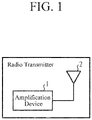
- FIG. 1 is a configuration diagram illustrating a radio transmitter including an amplification device 1 according to a first embodiment.
- FIG. 2 is a configuration diagram illustrating the amplification device 1 including an amplitude and phase control device 10 according to the first embodiment.
- FIG. 3 is a hardware configuration diagram illustrating hardware of the amplitude and phase control device 10 according to the first embodiment.
- the radio transmitter is provided with the amplification device 1 and a transmission antenna 2.
- the amplification device 1 amplifies a transmission signal that is a signal to be amplified, and outputs the amplified transmission signal to the transmission antenna 2.
- the transmission antenna 2 emits a radio wave caused by the amplified transmission signal output from the amplification device 1 into space.
- the amplification device 1 is provided with the amplitude and phase control device 10, digital-to-analog converters (hereinafter referred to as "DACs") 13a and 13b, a Doherty amplifier 14, and an analog-to-digital converter (hereinafter referred to as an "ADC”) 15.
- DACs digital-to-analog converters
- ADC analog-to-digital converter
- the amplitude and phase control device 10 is provided with a distortion compensating unit 11, a signal dividing unit 12, an error calculating unit 16, and a controlling unit 17.
- the amplitude and phase control device 10 divides the transmission signal into a first signal and a second signal.
- the amplitude and phase control device 10 outputs the first signal to the Doherty amplifier 14 via the DAC 13a, and outputs the second signal to the Doherty amplifier 14 via the DAC 13b.
- the distortion compensating unit 11 is implemented by, for example, a distortion compensating circuit 21 illustrated in FIG. 3 .
- the distortion compensating unit 11 is provided with a compensation coefficient calculating unit 11a and a distortion compensation processing unit 11b.
- the distortion compensating unit 11 generates a distortion compensation signal for reducing distortion included in a synthesized signal that is an output signal of the Doherty amplifier 14 by performing distortion compensation processing on the transmission signal, and outputs the distortion compensation signal to the signal dividing unit 12 as the transmission signal.
- the distortion compensating unit 11 generates the distortion compensation signal capable of reducing the distortion included in the synthesized signal that is the output signal of the Doherty amplifier 14 using a model indicating an inverse characteristic of a non-linear characteristic in the Doherty amplifier 14, and outputs the distortion compensation signal to the signal dividing unit 12.
- the compensation coefficient calculating unit 11a calculates a compensation coefficient of the model that minimizes an error calculated by the error calculating unit 16 using the transmission signals for past Q samples and a digital synthesized signal output from the ADC 15.
- the compensation coefficient calculating unit 11a outputs the compensation coefficient of the model to the distortion compensation processing unit 11b.
- the distortion compensation processing unit 11b calculates the distortion compensation signal using the transmission signals for the past Q samples and the compensation coefficient calculated by the compensation coefficient calculating unit 11a, and outputs the distortion compensation signal to the signal dividing unit 12.
- Q is an integer equal to or larger than one.
- the signal dividing unit 12 is implemented by a signal dividing circuit 22 illustrated in FIG. 3 , for example.
- the signal dividing unit 12 divides the distortion compensation signal output from the distortion compensating unit 11 into the first signal and the second signal.
- the signal dividing unit 12 outputs the first signal to a carrier amplifier 14a of the Doherty amplifier 14 via the DAC 13a.
- the signal dividing unit 12 outputs the second signal to a peak amplifier 14b of the Doherty amplifier 14 via the DAC 13b.
- the DAC 13a converts the first signal output from the signal dividing unit 12 from a digital signal to an analog signal, and outputs the analog signal to the carrier amplifier 14a of the Doherty amplifier 14 as a first analog signal.
- the DAC 13b converts the second signal output from the signal dividing unit 12 from a digital signal to an analog signal, and outputs the analog signal to the peak amplifier 14b of the Doherty amplifier 14 as a second analog signal.
- the Doherty amplifier 14 is provided with the carrier amplifier 14a, the peak amplifier 14b, and a signal synthesizing unit 14c.
- the Doherty amplifier 14 amplifies the first analog signal output from the DAC 13a, and amplifies the second analog signal output from the DAC 13b.
- the Doherty amplifier 14 outputs a synthesized signal of the amplified first analog signal and the amplified second analog signal to each of the outside of the amplification device 1 and the ADC 15.
- the carrier amplifier 14a amplifies the first analog signal output from the DAC 13a, and outputs the amplified first analog signal to the signal synthesizing unit 14c.
- the peak amplifier 14b amplifies the second analog signal output from the DAC 13b, and outputs the amplified second analog signal to the signal synthesizing unit 14c.
- the signal synthesizing unit 14c synthesizes the amplified first analog signal output from the carrier amplifier 14a and the amplified second analog signal output from the peak amplifier 14b.
- the signal synthesizing unit 14c outputs the synthesized signal of the amplified first analog signal and the amplified second analog signal to each of the outside of the amplification device 1 and the ADC 15.
- the ADC 15 converts the synthesized signal output from the signal synthesizing unit 14c from an analog signal to a digital signal, and outputs the digital signal to the error calculating unit 16 as the digital synthesized signal.
- the error calculating unit 16 is implemented by an error calculating circuit 23 illustrated in FIG. 3 , for example.
- the error calculating unit 16 acquires the digital synthesized signal output from the ADC 15, and multiplies the digital synthesized signal by a reciprocal of a gain of the Doherty amplifier 14.
- the error calculating unit 16 calculates an error between a digital synthesized signal after being multiplied by the reciprocal and the transmission signal, and outputs an error signal indicating the error to each of the controlling unit 17 and the distortion compensating unit 11.
- the controlling unit 17 is implemented by a controlling circuit 24 illustrated in FIG. 3 , for example.
- the controlling unit 17 controls the amplitude of each of the first signal and the second signal output from the signal dividing unit 12 depending on the error calculated by the error calculating unit 16.
- the controlling unit 17 controls the phase difference between the first signal output from the signal dividing unit 12 and the second signal output from the signal dividing unit 12 depending on the error calculated by the error calculating unit 16.
- each of the distortion compensating unit 11, the signal dividing unit 12, the error calculating unit 16, and the controlling unit 17 that are components of the amplitude and phase control device 10 is implemented by dedicated hardware as illustrated in FIG. 3 . That is, it is assumed that the amplitude and phase control device 10 is implemented by the distortion compensating circuit 21, the signal dividing circuit 22, the error calculating circuit 23, and the controlling circuit 24.
- Each of the distortion compensating circuit 21, the signal dividing circuit 22, the error calculating circuit 23, and the controlling circuit 24 corresponds to, for example, a single circuit, a composite circuit, a programmed processor, a parallel-programmed processor, an application specific integrated circuit (ASIC), a field-programmable gate array (FPGA), or a combination thereof.
- ASIC application specific integrated circuit
- FPGA field-programmable gate array
- the components of the amplitude and phase control device 10 are not limited to those implemented by the dedicated hardware, and the amplitude and phase control device 10 may also be implemented by software, firmware, or a combination of the software and firmware.
- the software or firmware is stored as a program in a memory of a computer.
- the computer is intended to mean hardware that executes the program, and corresponds to, for example, a central processing unit (CPU), a central processor, a processing unit, an arithmetic unit, a microprocessor, a microcomputer, a processor, a digital signal processor (DSP) or the like.
- FIG. 4 is a hardware configuration diagram of the computer in a case where the amplitude and phase control device 10 is implemented by the software, firmware or the like.
- the program for causing the computer to execute each processing procedure performed in the distortion compensating unit 11, the signal dividing unit 12, the error calculating unit 16, and the controlling unit 17 is stored in a memory 31.
- a processor 32 of the computer executes the program stored in the memory 31.
- FIG. 3 illustrates an example in which each of the components of the amplitude and phase control device 10 is implemented by the dedicated hardware
- FIG. 4 illustrates an example in which the amplitude and phase control device 10 is implemented by the software, firmware or the like.
- this is merely an example, and some components in the amplitude and phase control device 10 may be implemented by the dedicated hardware, and the remaining components may be implemented by the software, firmware or the like.
- FIG. 5 is a flowchart illustrating a processing procedure performed by the amplitude and phase control device 10.
- the distortion compensating unit 11 acquires the transmission signal that is the signal to be amplified, performs the distortion compensation processing on the transmission signal, and outputs the distortion compensation signal that is the transmission signal after the distortion compensation processing to the signal dividing unit 12 (step ST1 in FIG. 5 ).
- the model indicating the inverse characteristic of the non-linear characteristic in the Doherty amplifier 14 is stored in an internal memory of the distortion compensating unit 11.
- the compensation coefficient calculating unit 11a of the distortion compensating unit 11 acquires the transmission signals for the past Q samples.
- the compensation coefficient calculating unit 11a acquires x(n), x(n-1),..., x(n-q),..., and x(n-Q-1) as the transmission signals for the past Q samples.
- x(n) is the transmission signal of the latest sample.
- the compensation coefficient calculating unit 11a also acquires a digital synthesized signal dy(n) of the latest sample from the ADC 15.
- the compensation coefficient calculating unit 11a calculates a compensation coefficients a k,q of the model that minimize an error signal ⁇ e(n) (refer to following equation (3)) output from the error calculating unit 16 using the transmission signals x(n), x(n-1),..., x(n-q),..., and x(n-Q-1) for the past Q samples and the digital synthesized signal y(n). Since the processing of calculating the compensation coefficient a k,q is known technique, detailed description thereof is omitted (refer to, for example, Non-Patent Literature 1).
- the compensation coefficient calculating unit 11a outputs the compensation coefficient a k,q of the model to the distortion compensation processing unit 11b.
- the distortion compensation processing unit 11b acquires the transmission signals x(n), x(n-1),..., x(n-q),..., and x(n-Q-1) for the past Q samples, and acquires the compensation coefficient a k,q output from the compensation coefficient calculating unit 11a.
- the distortion compensation processing unit 11b calculates a distortion compensation signal z(n) by substituting the transmission signals x(n), x(n-1),..., x(n-q),..., and x(n-Q-1) for the past Q samples and the compensation coefficient a k,q of the model in following equation (2).
- K is an integer equal to or larger than one.
- the distortion compensation processing unit 11b outputs the distortion compensation signal z(n) to the signal dividing unit 12 as the transmission signal after the distortion compensation processing.
- the distortion compensation processing unit 11b can generate the distortion compensation signal z(n) capable of reducing distortion included in a synthesized signal y(n) output from the Doherty amplifier 14 using (K ⁇ Q) compensation coefficients a k,q .
- the distortion compensation processing unit 11b cannot generate the distortion compensation signal z(n) capable of reducing the distortion included in the synthesized signal y(n) even by using the (K ⁇ Q) compensation coefficients a k,q .
- the signal dividing unit 12 divides the distortion compensation signal z(n) output from the distortion compensation processing unit 11b of the distortion compensating unit 11 to a first signal si(n) and a second signal s 2 (n) (step ST2 in FIG. 5 ).
- the signal dividing unit 12 outputs the first signal si(n) to the DAC 13a, and outputs the second signal s 2 (n) to the DAC 13b.
- the DAC 13a converts the first signal si(n) output from the signal dividing unit 12 from a digital signal to an analog signal, and outputs the analog signal to the carrier amplifier 14a of the Doherty amplifier 14 as a first analog signal asi(n).
- the DAC 13b converts the second signal s 2 (n) output from the signal dividing unit 12 from a digital signal to an analog signal, and outputs the analog signal to the peak amplifier 14b of the Doherty amplifier 14 as a second analog signal as 2 (n).
- the carrier amplifier 14a amplifies the first analog signal asi(n) output from the DAC 13a, and outputs the amplified first analog signal asi(n)' to the signal synthesizing unit 14c.
- the peak amplifier 14b amplifies the second analog signal as 2 (n) output from the DAC 13b, and outputs the amplified second analog signal as 2 (n)' to the signal synthesizing unit 14c.
- the signal synthesizing unit 14c synthesizes the amplified first analog signal asi(n)' output from the carrier amplifier 14a and the amplified second analog signal as 2 (n)' output from the peak amplifier 14b.
- the signal synthesizing unit 14c outputs the synthesized signal y(n) of the amplified first analog signal asi(n)' and the amplified second analog signal as 2 (n)' to each of the outside of the amplification device 1 and the ADC 15.
- the ADC 15 converts the synthesized signal y(n) output from the signal synthesizing unit 14c from an analog signal to a digital signal.
- the ADC 15 outputs the digital signal to the error calculating unit 16 as the digital synthesized signal dy(n).
- the error calculating unit 16 acquires the digital synthesized signal dy(n) output from the ADC 15, and acquires the transmission signal x(n).
- the error calculating unit 16 multiplies the digital synthesized signal dy(n) by a reciprocal of a gain G of the Doherty amplifier 14, and calculates the error signal ⁇ e(n) indicating the error between the digital synthesized signal after being multiplied by the reciprocal and the transmission signal x(n) as expressed by following equation (3) (step ST3 in FIG. 5 ).
- ⁇ e n x n ⁇ dy n G
- the error calculating unit 16 outputs the error signal ⁇ e(n) to each of the controlling unit 17 and the compensation coefficient calculating unit 11a.
- the controlling unit 17 controls the amplitude of each of the first signal si(n) and the second signal s 2 (n) output from the signal dividing unit 12 depending on the error indicated by the error signal ⁇ e(n) (step ST4 in FIG. 5 ).
- the controlling unit 17 also controls the phase difference between the first signal si(n) output from the signal dividing unit 12 and the second signal s 2 (n) output from the signal dividing unit 12 depending on the error indicated by the error signal ⁇ e(n) (step ST5 in FIG. 5 ).
- amplitude control processing and phase control processing by the controlling unit 17 are specifically described.
- the controlling unit 17 includes a table (refer to FIG. 6 ) including a first amplitude coefficient amp 1 that is an amplitude coefficient of the first signal si(n) corresponding to an error e (i) , a second amplitude coefficient amp 2 that is an amplitude coefficient of the second signal s 2 (n) corresponding to the error e (i) , and a phase difference ⁇ ph corresponding to the error e (i) .
- a table (refer to FIG. 6 ) including a first amplitude coefficient amp 1 that is an amplitude coefficient of the first signal si(n) corresponding to an error e (i) , a second amplitude coefficient amp 2 that is an amplitude coefficient of the second signal s 2 (n) corresponding to the error e (i) , and a phase difference ⁇ ph corresponding to the error e (i) .
- FIG. 6 is an explanatory diagram illustrating an example of the table included in the controlling unit 17.
- the error e (i) having a range of five corresponds to the first amplitude coefficient ampi, the second amplitude coefficient amp 2 , and the phase difference ⁇ ph.
- the first amplitude coefficient ampi, the second amplitude coefficient amp 2 , and the phase difference ⁇ ph are obtained by computer simulation, for example.
- the controlling unit 17 calculates the error e (i) as expressed by following equation (4).
- the controlling unit 17 calculates an error e (1) , an error e (2) ,..., and an error e (10) . After calculating the error e (10) , the controlling unit 17 returns i to 1, and repeatedly performs the processing of calculating the error e (1) , the error e (2) ,..., and the error e (10) again.
- the controlling unit 17 repeatedly performs the processing of calculating the error e (1) , the error e (2) ,..., and an error e (100) .
- the controlling unit 17 acquires the first amplitude coefficient amp 1 corresponding to the error e (10) , the second amplitude coefficient amp 2 corresponding to the error e (10) , and the phase difference ⁇ ph corresponding to the error e (10) from the table illustrated in FIG. 6 .
- the controlling unit 17 acquires amp 1,1 as the first amplitude coefficient amp 1 corresponding to the error e (10) , and acquires amp 2,1 as the second amplitude coefficient amp 2 corresponding to the error e (10) .
- the controlling unit 17 acquires ⁇ ph 1 as the phase difference ⁇ ph corresponding to the error e (10) .
- the controlling unit 17 acquires amp 1,2 as the first amplitude coefficient amp 1 corresponding to the error e (10) , and acquires amp 2,2 as the second amplitude coefficient amp 2 corresponding to the error e (10) .
- the controlling unit 17 also acquires ⁇ ph 2 as the phase difference ⁇ ph corresponding to the error e (10) .
- the controlling unit 17 performs each of the amplitude control processing and the phase control processing by outputting the first amplitude coefficient ampi, the second amplitude coefficient amp 2 , and the phase difference ⁇ ph to the signal dividing unit 12.
- the controlling unit 17 outputs the first amplitude coefficient ampi, the second amplitude coefficient amp 2 , and the phase difference ⁇ ph to the signal dividing unit 12.
- the controlling unit 17 outputs the first amplitude coefficient ampi, the second amplitude coefficient amp 2 , and the phase difference ⁇ ph to the signal dividing unit 12.
- the signal dividing unit 12 generates the first signal si(n) and the second signal s 2 (n) using each of the first amplitude coefficient ampi, the second amplitude coefficient amp 2 , and the phase difference ⁇ ph output from the controlling unit 17.
- the signal dividing unit 12 multiplies the distortion compensation signal z(n) output from the compensation coefficient calculating unit 11a by the first amplitude coefficient amp 1 output from the controlling unit 17 as expressed by following equation (5).
- the signal dividing unit 12 outputs the distortion compensation signal after being multiplied by the first amplitude coefficient to the DAC 13a as the first signal si(n).
- s 1 n amp 1 ⁇ z n
- the distortion compensation signal z(n) is a complex signal and is expressed by following equation (6).
- z n A n ⁇ exp ⁇ n
- A(n) represents the amplitude of the distortion compensation signal z(n)
- ⁇ (n) represents the phase of the distortion compensation signal z(n).
- the signal dividing unit 12 multiplies the distortion compensation signal z(n) output from the compensation coefficient calculating unit 11a by the second amplitude coefficient amp 2 output from the controlling unit 17 as expressed by following equation (7).
- the signal dividing unit 12 adds the phase difference ⁇ ph to the phase ⁇ (n) of the distortion compensation signal after being multiplied by the second amplitude coefficient as expressed by following equation (7).
- the signal dividing unit 12 outputs the distortion compensation signal after the phase difference is added to the DAC 13b as the second signal s 2 (n).
- s 2 n amp 2 ⁇ A n ⁇ exp ⁇ n + ⁇ ph
- the amplitude and phase control device 10 is provided with the signal dividing unit 12 that divides the transmission signal into the first signal and the second signal, and outputs each of the first signal and the second signal to the Doherty amplifier 14, the error calculating unit 16 that acquires, from the Doherty amplifier 14, the synthesized signal of the first signal amplified by the Doherty amplifier 14 and the second signal amplified by the Doherty amplifier 14, performs multiplication of the synthesized signal by the reciprocal of the gain of the Doherty amplifier 14, and performs calculation of the error between the synthesized signal after the multiplication by the reciprocal and the transmission signal, and the controlling unit 17 that controls the amplitude of each of the first signal and the second signal output from the signal dividing unit 12 depending on the error calculated by the error calculating unit 16 and controls the phase difference between the first signal output from the signal dividing unit 12 and the second signal output from the signal dividing unit 12 depending on the error. Therefore, even when the non-linear characteristic of the Doherty
- the amplitude and phase control device 10 illustrated in FIG. 2 is provided with the distortion compensating unit 11. However, even when the amplitude and phase control device 10 is not provided with the distortion compensating unit 11, this may reduce the distortion included in the synthesized signal y(n) output from the Doherty amplifier 14 when the non-linear characteristic of the Doherty amplifier 14 changes.
- the signal dividing unit 12 multiplies the first amplitude coefficient amp 1 output from the controlling unit 17 by the transmission signal x(n).
- the signal dividing unit 12 outputs the transmission signal after being multiplied by the first amplitude coefficient to the DAC 13a as the first signal si(n).
- the signal dividing unit 12 multiplies the transmission signal x(n) by the second amplitude coefficient amp 2 output from the controlling unit 17.
- the signal dividing unit 12 also adds the phase difference ⁇ ph to the phase ⁇ (n) of the transmission signal after being multiplied by the second amplitude coefficient.
- the signal dividing unit 12 outputs the transmission signal after the phase difference is added to the DAC 13b as the second signal s 2 (n).
- the error calculating unit 16 calculates the error signal ⁇ e(n) indicating the error between the digital synthesized signal dy(n)/G after being multiplied by the reciprocal and the transmission signal x(n).
- the error calculating unit 16 may calculate the error signal ⁇ e(n) indicating an error between the digital synthesized signal dy(n)/G after being multiplied by the reciprocal and the distortion compensation signal z(n) output from the distortion compensating unit 11.
- FIG. 7 is a configuration diagram illustrating the amplification device 1 including another amplitude and phase control device 10 according to the first embodiment.
- the DAC 13a outputs the first analog signal asi(n) to the carrier amplifier 14a
- the DAC 13b outputs the second analog signal as 2 (n) to the peak amplifier 14b.
- the DAC 13a may convert a frequency of the first analog signal asi(n) into, for example, a radio frequency (RF), and output the first analog signal asi(n) after frequency conversion to the carrier amplifier 14a.
- the DAC 13b may convert a frequency of the second analog signal as 2 (n) into, for example, RF, and output the second analog signal as 2 (n) after frequency conversion to the peak amplifier 14b.
- the ADC 15 outputs the digital synthesized signal dy(n) to the error calculating unit 16.
- the ADC 15 may convert a frequency of the digital synthesized signal dy(n) into, for example, a baseband frequency, and output the digital synthesized signal dy(n) after frequency conversion to the error calculating unit 16.
- an amplitude and phase control device 10 in which a controlling unit 17 calculates each of a first amplitude coefficient ampi, a second amplitude coefficient amp 2 , and a phase difference ⁇ ph using a polynomial having an error as a variable is described.
- a configuration of the amplitude and phase control device 10 according to the second embodiment is similar to the configuration of the amplitude and phase control device 10 according to the first embodiment, and FIGS. 2 and 7 are configuration diagrams illustrating the amplitude and phase control device 10 according to the second embodiment.
- An internal memory of the controlling unit 17 stores each of a polynomial expressed by following equation (8), a polynomial expressed by following equation (9), and a polynomial expressed by following equation (10).
- amp 1 ⁇ 0 + ⁇ 1 ⁇ e + ⁇ 2 ⁇ e 2 + ...
- amp 2 ⁇ 0 + ⁇ 1 ⁇ e + ⁇ 2 ⁇ e 2 + ...
- ⁇ ph ⁇ 0 + ⁇ 1 ⁇ e + ⁇ 2 ⁇ e 2 + ...
- e e (i) . ⁇ 0 , ⁇ 1 , ⁇ 2 ..., ⁇ 0 , ⁇ 1 , ⁇ 2 ..., and ⁇ 0 , ⁇ 1 , ⁇ 2 ... are constants calculated by computer simulation, for example.
- the controlling unit 17 calculates an error e (i) from an error signal ⁇ e(n) output from an error calculating unit 16.
- the controlling unit 17 calculates the first amplitude coefficient amp 1 by substituting the error e (I) into equation (8) as the error e (i) .
- the controlling unit 17 calculates the second amplitude coefficient amp 2 by substituting the error e (I) into equation (9) as the error e (i) .
- the controlling unit 17 calculates the phase difference ⁇ ph by substituting the error e (I) into equation (10) as the error e (i) .
- the controlling unit 17 performs each of the amplitude control processing and the phase control processing by outputting the first amplitude coefficient ampi, the second amplitude coefficient amp 2 , and the phase difference ⁇ ph to the signal dividing unit 12.
- the amplitude and phase control device 10 is configured so that the controlling unit 17 calculates each of the first amplitude coefficient ampi, the second amplitude coefficient amp 2 , and the phase difference ⁇ ph using the polynomial having the error as the variable. Even when a non-linear characteristic of a Doherty amplifier 14 changes, the amplitude and phase control device 10 according to the second embodiment can reduce distortion included in a synthesized signal y(n) output from the Doherty amplifier 14 as with the amplitude and phase control device 10 according to the first embodiment.
- an amplitude and phase control device 10 provided with a power calculating unit 18 that calculates power of a transmission signal is described.
- FIG. 8 is a configuration diagram illustrating an amplification device 1 including the amplitude and phase control device 10 according to the third embodiment.
- the same reference sign as that in FIGS. 2 and 7 represents the same or corresponding part, so that the description thereof is omitted.
- FIG. 9 is a hardware configuration diagram illustrating hardware of the amplitude and phase control device 10 according to the third embodiment.
- the same reference sign as that in FIG. 3 represents the same or corresponding part, so that the description thereof is omitted.
- the power calculating unit 18 is implemented by a power calculating circuit 25 illustrated in FIG. 9 , for example.
- the power calculating unit 18 calculates the power of the transmission signal and outputs power information indicating the power to a controlling unit 19.
- the controlling unit 19 is implemented by a controlling circuit 26 illustrated in FIG. 9 , for example.
- the controlling unit 19 controls an amplitude of each of a first signal and a second signal output from a signal dividing unit 12 depending on each of an error calculated by an error calculating unit 16, the power calculated by the power calculating unit 18, and a carrier frequency of the transmission signal.
- the controlling unit 17 controls a phase difference between the first signal output from the signal dividing unit 12 and the second signal output from the signal dividing unit 12 depending on each of the error calculated by the error calculating unit 16, the power calculated by the power calculating unit 18, and the carrier frequency of the transmission signal.
- each of a distortion compensating unit 11, the signal dividing unit 12, the error calculating unit 16, the power calculating unit 18, and the controlling unit 19 that are components of the amplitude and phase control device 10 is implemented by dedicated hardware as illustrated in FIG. 9 . That is, it is assumed that the amplitude and phase control device 10 is implemented by a distortion compensating circuit 21, a signal dividing circuit 22, an error calculating circuit 23, the power calculating circuit 25, and the controlling circuit 26.
- Each of the distortion compensating circuit 21, the signal dividing circuit 22, the error calculating circuit 23, the power calculating circuit 25, and the controlling circuit 26 corresponds to, for example, a single circuit, a composite circuit, a programmed processor, a parallel-programmed processor, an ASIC, a FPGA, or a combination thereof.
- the components of the amplitude and phase control device 10 are not limited to those implemented by the dedicated hardware, and the amplitude and phase control device 10 may also be implemented by software, firmware, or a combination of the software and firmware.
- a program for causing the computer to execute each processing procedure performed in the distortion compensating unit 11, the signal dividing unit 12, the error calculating unit 16, the power calculating unit 18, and the controlling unit 19 is stored in the memory 31 illustrated in FIG. 4 .
- the processor 32 illustrated in FIG. 4 executes the program stored in the memory 31.
- FIG. 9 illustrates an example in which each of the components of the amplitude and phase control device 10 is implemented by the dedicated hardware
- FIG. 4 illustrates an example in which the amplitude and phase control device 10 is implemented by the software, firmware or the like.
- this is merely an example, and some components in the amplitude and phase control device 10 may be implemented by the dedicated hardware, and the remaining components may be implemented by the software, firmware or the like.
- the power calculating unit 18 calculates instantaneous power of a transmission signal x(n) as power P(n) of the transmission signal x(n), and outputs power information indicating the power P(n) to the controlling unit 19.
- the controlling unit 19 acquires an error signal ⁇ e(n) from the error calculating unit 16, acquires the power information from the power calculating unit 18, and acquires a carrier frequency f.
- the controlling unit 19 controls amplitude of each of a first signal si(n) and a second signal s 2 (n) output from the signal dividing unit 12 depending on each of an error indicated by the error signal ⁇ e(n), the power P(n) indicated by the power information, and the carrier frequency f of the transmission signal x(n).
- the controlling unit 19 also controls the phase difference between the first signal si(n) output from the signal dividing unit 12 and the second signal s 2 (n) output from the signal dividing unit 12 depending on each of the error indicated by the error signal ⁇ e(n), the power P(n) indicated by the power information, and the carrier frequency f of the transmission signal x(n).
- amplitude control processing and phase control processing by the controlling unit 19 are specifically described.
- the controlling unit 19 includes a table (refer to FIG. 10 ) including a first amplitude coefficient amp 1 corresponding to a combination of an error e (1) , the power P, and the carrier frequency f, a second amplitude coefficient amp 2 corresponding to the combination of the error e (1) , the power P, and the carrier frequency f, and a phase difference ⁇ ph corresponding to the combination of the error e (i) , the power P, and the carrier frequency f.
- a table (refer to FIG. 10 ) including a first amplitude coefficient amp 1 corresponding to a combination of an error e (1) , the power P, and the carrier frequency f, a second amplitude coefficient amp 2 corresponding to the combination of the error e (1) , the power P, and the carrier frequency f, and a phase difference ⁇ ph corresponding to the combination of the error e (i) , the power P, and the carrier frequency f.
- FIG. 10 is an explanatory diagram illustrating an example of the table included in the controlling unit 19.
- the error e (i) having a range of five corresponds to the first amplitude coefficient ampi, the second amplitude coefficient amp 2 , and the phase difference ⁇ ph.
- the first amplitude coefficient ampi, the second amplitude coefficient amp 2 , and the phase difference ⁇ ph are obtained by computer simulation, for example.
- the controlling unit 19 also acquires the second amplitude coefficient amp 2 corresponding to the combination of the error e (10) , the power P(n), and the carrier frequency f from the table illustrated in FIG. 10 .
- the controlling unit 19 also acquires the phase difference ⁇ ph corresponding to the combination of the error e (10) , the power P(n), and the carrier frequency f from the table illustrated in FIG. 10 .
- the controlling unit 19 acquires amp 1,1 as the first amplitude coefficient ampi, and acquires amp 2,1 as the second amplitude coefficient amp 2 .
- the controlling unit 19 also acquires ⁇ ph 1 as the phase difference ⁇ ph.
- the controlling unit 19 acquires amp 1,12 as the first amplitude coefficient ampi, and acquires amp 2,12 as the second amplitude coefficient amp 2 .
- the controlling unit 19 acquires ⁇ ph 12 as the phase difference ⁇ ph.
- the controlling unit 19 performs each of the amplitude control processing and the phase control processing by outputting the first amplitude coefficient ampi, the second amplitude coefficient amp 2 , and the phase difference ⁇ ph to the signal dividing unit 12.
- the amplitude and phase control device 10 is provided with the power calculating unit 18 that calculates the power of the transmission signal.
- the amplitude and phase control device 10 illustrated in FIG. 8 is configured so that the controlling unit 19 controls the amplitude of each of the first signal and the second signal output from the signal dividing unit 12 depending on each of the error calculated by the error calculating unit 16, the power calculated by the power calculating unit 18, and the carrier frequency of the transmission signal, and controls the phase difference between the first signal output from the signal dividing unit 12 and the second signal output from the signal dividing unit 12 depending on each of the error calculated by the error calculating unit 16, the power calculated by the power calculating unit 18, and the carrier frequency of the transmission signal. Therefore, even when a non-linear characteristic of the Doherty amplifier 14 changes, the amplitude and phase control device 10 illustrated in FIG. 8 can reduce distortion included in a synthesized signal output from the Doherty amplifier 14.
- the amplitude and phase control device 10 illustrated in FIG. 8 can further reduce the distortion included in the synthesized signal output from the Doherty amplifier 14 as compared with the amplitude and phase control device 10 illustrated in FIG. 2 .
- the power calculating unit 18 calculates the power P(n) of the transmission signal x(n). However, this is merely an example, and as illustrated in FIG. 11 , the power calculating unit 18 may calculate the power P(n) of a distortion compensation signal z(n) output from the compensation coefficient calculating unit 11a.
- FIG. 11 is a configuration diagram illustrating the amplification device 1 including another amplitude and phase control device 10 according to the third embodiment.
- an amplitude and phase control device 10 in which a controlling unit 19 calculates each of a first amplitude coefficient ampi, a second amplitude coefficient amp 2 , and a phase difference ⁇ ph using a polynomial having each of an error, power, and a carrier frequency as a variable is described.
- a configuration of the amplitude and phase control device 10 according to the fourth embodiment is similar to the configuration of the amplitude and phase control device 10 according to the third embodiment, and FIGS. 8 and 11 are configuration diagrams illustrating the amplitude and phase control device 10 according to the fourth embodiment.
- An internal memory of the controlling unit 19 stores each of a polynomial expressed by following equation (11), a polynomial expressed by following equation (12), and a polynomial expressed by following equation (13).
- amp 1 a 0 + a 1 ⁇ e + ⁇ 2 ⁇ e 2 + ... + b 0 + b 1 ⁇ e + b 2 ⁇ e 2 + ... c 0 + c 1 ⁇ e + c 2 ⁇ e 2 + ...
- the controlling unit 19 calculates an error e (i) from an error signal ⁇ e(n) output from the error calculating unit 16.
- the controlling unit 19 calculates the first amplitude coefficient amp 1 by substituting the error e (I) into equation (11) as the error e (i) and by substituting each of power P(n) and a carrier frequency f into equation (11).
- the controlling unit 19 calculates the second amplitude coefficient amp 2 by substituting the error e (I) into equation (12) as the error e (i) and by substituting each of power P(n) and a carrier frequency f into equation (12).
- the controlling unit 19 calculates the phase difference ⁇ ph by substituting the error e (I) into equation (13) as the error e (i) and by substituting each of power P(n) and a carrier frequency f into equation (13).
- the controlling unit 19 performs each of the amplitude control processing and the phase control processing by outputting the first amplitude coefficient ampi, the second amplitude coefficient amp 2 , and the phase difference ⁇ ph to the signal dividing unit 12.
- the amplitude and phase control device 10 is configured so that the controlling unit 19 calculates each of the first amplitude coefficient ampi, the second amplitude coefficient amp 2 , and the phase difference ⁇ ph using the polynomial having each of the error, the power, and the carrier frequency as the variable is described. Even when a non-linear characteristic of a Doherty amplifier 14 changes, the amplitude and phase control device 10 according to the fourth embodiment can reduce distortion included in a synthesized signal output from the Doherty amplifier 14 as with the amplitude and phase control device 10 according to the third embodiment.
- the embodiments may be freely combined, any component of each embodiment may be modified, or any component may be omitted in each embodiment.
- the present disclosure is suitable for an amplitude and phase control device and an amplitude and phase control method for outputting each of a first signal and a second signal to a Doherty amplifier.
- the present disclosure is suitable for an amplification device provided with an amplitude and phase control device and a Doherty amplifier.
- the present disclosure is suitable for a radio transmitter provided with an amplification device.
- 1 amplification device
- 2 transmission antenna
- 10 amplitude and phase control device
- 11 distortion compensating unit
- 11a compensation coefficient calculating unit
- 11b distortion compensation processing unit
- 12 signal dividing unit
- 13a, 13b DAC
- 14 Doherty amplifier
- 14a carrier amplifier
- 14b peak amplifier
- 14c signal synthesizing unit
- 15 ADC
- 16 error calculating unit
- 17 controlling unit
- 18 power calculating unit
- 19 controlling unit
- 21 distortion compensating circuit
- 22 signal dividing circuit
- 23 error calculating circuit
- 24 controlling circuit
- 25 power calculating circuit
- 26 controlling circuit
Landscapes
- Engineering & Computer Science (AREA)
- Power Engineering (AREA)
- Computer Networks & Wireless Communication (AREA)
- Signal Processing (AREA)
- Physics & Mathematics (AREA)
- Nonlinear Science (AREA)
- Microelectronics & Electronic Packaging (AREA)
- Amplifiers (AREA)
- Automatic Cycles, And Cycles In General (AREA)
- Axle Suspensions And Sidecars For Cycles (AREA)
Abstract
Description
- The present disclosure relates to an amplitude and phase control device and an amplitude and phase control method to output each of a first signal and a second signal to a Doherty amplifier, an amplification device provided with the amplitude and phase control device and the Doherty amplifier, and a radio transmitter provided with the amplification device.
- In an amplifier used in a radio transmitter, distortion included in an amplified transmission signal is required to be small.
- Following Non-Patent Literature 1 discloses a distortion compensating circuit that reduces distortion included in an output signal of an amplifier. The distortion compensating circuit generates a distortion compensation signal capable of reducing distortion included in the output signal of the amplifier using a model indicating an inverse characteristic of a non-linear characteristic of the amplifier, and applies the distortion compensation signal to the amplifier as a signal to be amplified.
- Hereinafter, generation processing of the distortion compensation signal by the distortion compensating circuit is specifically described.
- The distortion compensating circuit multiplies an output signal y(n) of the amplifier by a reciprocal of a gain of the amplifier, and calculates an error e(n) between an output signal z(n) hat after being multiplied by the reciprocal and a distortion compensation signal z(n). In the description of this specification, it is not possible to attach a symbol "^" on a character z due to the electronic filing application, so that this is represented as z(n) hat. The symbol n represents a sample number.
- The distortion compensating circuit calculates a compensation coefficients ak,q of a model that minimizes the error e(n). Since the model has (K×Q) compensation coefficients ak,q, the distortion compensating circuit calculates (K×Q) compensation coefficients ak,q. K is a fixed value (integer) equal to or larger than one set depending on the non-linear characteristic of the amplifier, and corresponds to the order of a function representing the model. When the model indicating the inverse characteristic of the non-linear characteristic in the amplifier can be expressed by, for example, a fifth-order function, K = 5 is set. Q is an integer equal to or larger than one.
- The distortion compensating circuit calculates the distortion compensation signal z(n) by substituting signals x(n), x(n-1),..., x(n-q),..., and x(n-Q-1) to be amplified for past Q samples and the calculated compensation coefficient ak,q in following equation (1).

- The distortion compensating circuit outputs the distortion compensation signal z(n) to the amplifier.
- Non-Patent Literature 1: Lei Ding, G. Tong Zhou, Dennis R. Morgan, Zhengxiand Ma, J. Stevenson Kenney, Jaehyeong, Kim, and Charles R. Giardina, "A robust digital baseband predistorter constructed using memory polynomial," IEEE Transactions on Communications, vol. 52, no. 1, Jan. 2004.
- In the distortion compensating circuit disclosed in Non-Patent Literature 1, the number of compensation coefficients ak,q included in the model is fixed to (K×Q). For this reason, when the non-linear characteristic of the amplifier changes due to a change in temperature, deterioration over time or the like, there is a case where the model does not indicate the inverse characteristic of the non-linear characteristic of the amplifier. Therefore, there has been a problem that, when the non-linear characteristic of the amplifier changes, the distortion included in the output signal y(n) of the amplifier cannot be reduced in some cases even when the distortion compensation signal is generated using the (K×Q) compensation coefficients ak,q.
- The present disclosure has been made to solve the above-described problem, and an object thereof is to obtain an amplification device capable of reducing distortion included in a synthesized signal output from a Doherty amplifier even when a non-linear characteristic of the Doherty amplifier changes.
- An amplitude and phase control device according to the present disclosure includes a signal dividing unit to divide a transmission signal into a first signal and a second signal, and output each of the first signal and the second signal to a Doherty amplifier; an error calculating unit to acquire, from the Doherty amplifier, a synthesized signal of a first signal amplified by the Doherty amplifier and a second signal amplified by the Doherty amplifier, perform multiplication of the synthesized signal by a reciprocal of a gain of the Doherty amplifier, and perform calculation of an error between the synthesized signal after the multiplication by the reciprocal and the transmission signal; and a controlling unit to control an amplitude of each of the first signal and the second signal output from the signal dividing unit depending on the error calculated by the error calculating unit, and control a phase difference between the first signal output from the signal dividing unit and the second signal output from the signal dividing unit depending on the error.
- According to the present disclosure, the distortion included in the synthesized signal output from the Doherty amplifier can be reduced even when the non-linear characteristic of the Doherty amplifier changes.
-
-
FIG. 1 is a configuration diagram illustrating a radio transmitter including an amplification device 1 according to a first embodiment. -
FIG. 2 is a configuration diagram illustrating the amplification device 1 including an amplitude andphase control device 10 according to the first embodiment. -
FIG. 3 is a hardware configuration diagram illustrating hardware of the amplitude andphase control device 10 according to the first embodiment. -
FIG. 4 is a hardware configuration diagram of a computer in a case where the amplitude andphase control device 10 is implemented by software, firmware or the like. -
FIG. 5 is a flowchart illustrating a processing procedure performed by the amplitude andphase control device 10. -
FIG. 6 is an explanatory diagram illustrating an example of a table included in a controllingunit 17. -
FIG. 7 is a configuration diagram illustrating the amplification device 1 including another amplitude andphase control device 10 according to the first embodiment. -
FIG. 8 is a configuration diagram illustrating an amplification device 1 including an amplitude andphase control device 10 according to a third embodiment. -
FIG. 9 is a hardware configuration diagram illustrating hardware of the amplitude andphase control device 10 according to the third embodiment. -
FIG. 10 is an explanatory diagram illustrating an example of a table included in a controllingunit 19. -
FIG. 11 is a configuration diagram illustrating the amplification device 1 including another amplitude andphase control device 10 according to the third embodiment. - Some modes for carrying out the present disclosure are hereinafter described with reference to the attached drawings in order to describe the present disclosure in further detail.
-
FIG. 1 is a configuration diagram illustrating a radio transmitter including an amplification device 1 according to a first embodiment. -
FIG. 2 is a configuration diagram illustrating the amplification device 1 including an amplitude andphase control device 10 according to the first embodiment. -
FIG. 3 is a hardware configuration diagram illustrating hardware of the amplitude andphase control device 10 according to the first embodiment. - The radio transmitter is provided with the amplification device 1 and a
transmission antenna 2. - The amplification device 1 amplifies a transmission signal that is a signal to be amplified, and outputs the amplified transmission signal to the
transmission antenna 2. - The
transmission antenna 2 emits a radio wave caused by the amplified transmission signal output from the amplification device 1 into space. - The amplification device 1 is provided with the amplitude and
phase control device 10, digital-to-analog converters (hereinafter referred to as "DACs") 13a and 13b, a Dohertyamplifier 14, and an analog-to-digital converter (hereinafter referred to as an "ADC") 15. - The amplitude and
phase control device 10 is provided with adistortion compensating unit 11, asignal dividing unit 12, anerror calculating unit 16, and a controllingunit 17. - The amplitude and
phase control device 10 divides the transmission signal into a first signal and a second signal. - The amplitude and
phase control device 10 outputs the first signal to the Doherty amplifier 14 via theDAC 13a, and outputs the second signal to the Dohertyamplifier 14 via theDAC 13b. - The
distortion compensating unit 11 is implemented by, for example, adistortion compensating circuit 21 illustrated inFIG. 3 . - The
distortion compensating unit 11 is provided with a compensation coefficient calculating unit 11a and a distortioncompensation processing unit 11b. - The
distortion compensating unit 11 generates a distortion compensation signal for reducing distortion included in a synthesized signal that is an output signal of the Dohertyamplifier 14 by performing distortion compensation processing on the transmission signal, and outputs the distortion compensation signal to thesignal dividing unit 12 as the transmission signal. - That is, the
distortion compensating unit 11 generates the distortion compensation signal capable of reducing the distortion included in the synthesized signal that is the output signal of the Dohertyamplifier 14 using a model indicating an inverse characteristic of a non-linear characteristic in the Dohertyamplifier 14, and outputs the distortion compensation signal to thesignal dividing unit 12. - The compensation coefficient calculating unit 11a calculates a compensation coefficient of the model that minimizes an error calculated by the
error calculating unit 16 using the transmission signals for past Q samples and a digital synthesized signal output from theADC 15. - The compensation coefficient calculating unit 11a outputs the compensation coefficient of the model to the distortion
compensation processing unit 11b. - The distortion
compensation processing unit 11b calculates the distortion compensation signal using the transmission signals for the past Q samples and the compensation coefficient calculated by the compensation coefficient calculating unit 11a, and outputs the distortion compensation signal to thesignal dividing unit 12. Q is an integer equal to or larger than one. - The
signal dividing unit 12 is implemented by asignal dividing circuit 22 illustrated inFIG. 3 , for example. - The
signal dividing unit 12 divides the distortion compensation signal output from thedistortion compensating unit 11 into the first signal and the second signal. - The
signal dividing unit 12 outputs the first signal to acarrier amplifier 14a of theDoherty amplifier 14 via theDAC 13a. - The
signal dividing unit 12 outputs the second signal to apeak amplifier 14b of theDoherty amplifier 14 via theDAC 13b. - An amplitude of each of the first signal and the second signal output from the
signal dividing unit 12 will be described later. A phase difference between the first signal output from thesignal dividing unit 12 and the second signal output from thesignal dividing unit 12 will be described later. - The
DAC 13a converts the first signal output from thesignal dividing unit 12 from a digital signal to an analog signal, and outputs the analog signal to thecarrier amplifier 14a of theDoherty amplifier 14 as a first analog signal. - The
DAC 13b converts the second signal output from thesignal dividing unit 12 from a digital signal to an analog signal, and outputs the analog signal to thepeak amplifier 14b of theDoherty amplifier 14 as a second analog signal. - The
Doherty amplifier 14 is provided with thecarrier amplifier 14a, thepeak amplifier 14b, and asignal synthesizing unit 14c. - The
Doherty amplifier 14 amplifies the first analog signal output from theDAC 13a, and amplifies the second analog signal output from theDAC 13b. - The
Doherty amplifier 14 outputs a synthesized signal of the amplified first analog signal and the amplified second analog signal to each of the outside of the amplification device 1 and theADC 15. - The
carrier amplifier 14a amplifies the first analog signal output from theDAC 13a, and outputs the amplified first analog signal to thesignal synthesizing unit 14c. - The
peak amplifier 14b amplifies the second analog signal output from theDAC 13b, and outputs the amplified second analog signal to thesignal synthesizing unit 14c. - The
signal synthesizing unit 14c synthesizes the amplified first analog signal output from thecarrier amplifier 14a and the amplified second analog signal output from thepeak amplifier 14b. - The
signal synthesizing unit 14c outputs the synthesized signal of the amplified first analog signal and the amplified second analog signal to each of the outside of the amplification device 1 and theADC 15. - The
ADC 15 converts the synthesized signal output from thesignal synthesizing unit 14c from an analog signal to a digital signal, and outputs the digital signal to theerror calculating unit 16 as the digital synthesized signal. - The
error calculating unit 16 is implemented by anerror calculating circuit 23 illustrated inFIG. 3 , for example. - The
error calculating unit 16 acquires the digital synthesized signal output from theADC 15, and multiplies the digital synthesized signal by a reciprocal of a gain of theDoherty amplifier 14. - The
error calculating unit 16 calculates an error between a digital synthesized signal after being multiplied by the reciprocal and the transmission signal, and outputs an error signal indicating the error to each of the controllingunit 17 and thedistortion compensating unit 11. - The controlling
unit 17 is implemented by a controllingcircuit 24 illustrated inFIG. 3 , for example. - The controlling
unit 17 controls the amplitude of each of the first signal and the second signal output from thesignal dividing unit 12 depending on the error calculated by theerror calculating unit 16. - The controlling
unit 17 controls the phase difference between the first signal output from thesignal dividing unit 12 and the second signal output from thesignal dividing unit 12 depending on the error calculated by theerror calculating unit 16. - In
FIG. 2 , it is assumed that each of thedistortion compensating unit 11, thesignal dividing unit 12, theerror calculating unit 16, and the controllingunit 17 that are components of the amplitude andphase control device 10 is implemented by dedicated hardware as illustrated inFIG. 3 . That is, it is assumed that the amplitude andphase control device 10 is implemented by thedistortion compensating circuit 21, thesignal dividing circuit 22, theerror calculating circuit 23, and the controllingcircuit 24. - Each of the
distortion compensating circuit 21, thesignal dividing circuit 22, theerror calculating circuit 23, and the controllingcircuit 24 corresponds to, for example, a single circuit, a composite circuit, a programmed processor, a parallel-programmed processor, an application specific integrated circuit (ASIC), a field-programmable gate array (FPGA), or a combination thereof. - The components of the amplitude and
phase control device 10 are not limited to those implemented by the dedicated hardware, and the amplitude andphase control device 10 may also be implemented by software, firmware, or a combination of the software and firmware. - The software or firmware is stored as a program in a memory of a computer. The computer is intended to mean hardware that executes the program, and corresponds to, for example, a central processing unit (CPU), a central processor, a processing unit, an arithmetic unit, a microprocessor, a microcomputer, a processor, a digital signal processor (DSP) or the like.
-
FIG. 4 is a hardware configuration diagram of the computer in a case where the amplitude andphase control device 10 is implemented by the software, firmware or the like. - In a case where the amplitude and
phase control device 10 is implemented by the software, firmware or the like, the program for causing the computer to execute each processing procedure performed in thedistortion compensating unit 11, thesignal dividing unit 12, theerror calculating unit 16, and the controllingunit 17 is stored in amemory 31. Aprocessor 32 of the computer executes the program stored in thememory 31. -
FIG. 3 illustrates an example in which each of the components of the amplitude andphase control device 10 is implemented by the dedicated hardware, andFIG. 4 illustrates an example in which the amplitude andphase control device 10 is implemented by the software, firmware or the like. However, this is merely an example, and some components in the amplitude andphase control device 10 may be implemented by the dedicated hardware, and the remaining components may be implemented by the software, firmware or the like. - Next, an operation of the amplification device 1 illustrated in
FIG. 2 is described. -
FIG. 5 is a flowchart illustrating a processing procedure performed by the amplitude andphase control device 10. - The
distortion compensating unit 11 acquires the transmission signal that is the signal to be amplified, performs the distortion compensation processing on the transmission signal, and outputs the distortion compensation signal that is the transmission signal after the distortion compensation processing to the signal dividing unit 12 (step ST1 inFIG. 5 ). - Hereinafter, the distortion compensation processing by the
distortion compensating unit 11 is specifically described. - The model indicating the inverse characteristic of the non-linear characteristic in the
Doherty amplifier 14 is stored in an internal memory of thedistortion compensating unit 11. - The compensation coefficient calculating unit 11a of the
distortion compensating unit 11 acquires the transmission signals for the past Q samples. - That is, the compensation coefficient calculating unit 11a acquires x(n), x(n-1),..., x(n-q),..., and x(n-Q-1) as the transmission signals for the past Q samples. x(n) is the transmission signal of the latest sample.
- The compensation coefficient calculating unit 11a also acquires a digital synthesized signal dy(n) of the latest sample from the
ADC 15. - The compensation coefficient calculating unit 11a calculates a compensation coefficients ak,q of the model that minimize an error signal Δe(n) (refer to following equation (3)) output from the
error calculating unit 16 using the transmission signals x(n), x(n-1),..., x(n-q),..., and x(n-Q-1) for the past Q samples and the digital synthesized signal y(n). Since the processing of calculating the compensation coefficient ak,q is known technique, detailed description thereof is omitted (refer to, for example, Non-Patent Literature 1). - The compensation coefficient calculating unit 11a outputs the compensation coefficient ak,q of the model to the distortion
compensation processing unit 11b. - The distortion
compensation processing unit 11b acquires the transmission signals x(n), x(n-1),..., x(n-q),..., and x(n-Q-1) for the past Q samples, and acquires the compensation coefficient ak,q output from the compensation coefficient calculating unit 11a. - The distortion
compensation processing unit 11b calculates a distortion compensation signal z(n) by substituting the transmission signals x(n), x(n-1),..., x(n-q),..., and x(n-Q-1) for the past Q samples and the compensation coefficient ak,q of the model in following equation (2). K is an integer equal to or larger than one.
- The distortion
compensation processing unit 11b outputs the distortion compensation signal z(n) to thesignal dividing unit 12 as the transmission signal after the distortion compensation processing. - When the non-linear characteristic of the
Doherty amplifier 14 is not changed due to a change in temperature, deterioration over time or the like, the distortioncompensation processing unit 11b can generate the distortion compensation signal z(n) capable of reducing distortion included in a synthesized signal y(n) output from theDoherty amplifier 14 using (K×Q) compensation coefficients ak,q. However, when the non-linear characteristic of theDoherty amplifier 14 is changed due to the change in temperature, deterioration over time or the like, the distortioncompensation processing unit 11b cannot generate the distortion compensation signal z(n) capable of reducing the distortion included in the synthesized signal y(n) even by using the (K×Q) compensation coefficients ak,q. - Note that, when an order of a function representing the model is appropriate, the larger the value of Q is, the more reduction accuracy of the distortion is improved. However, K is solely responsible for the order of the function representing the model, and the model itself is not appropriate when K does not indicate the appropriate order due to the change in temperature or the like. Therefore, even when the value of Q is set to a large value, the distortion cannot be reduced in some cases.
- The
signal dividing unit 12 divides the distortion compensation signal z(n) output from the distortioncompensation processing unit 11b of thedistortion compensating unit 11 to a first signal si(n) and a second signal s2(n) (step ST2 inFIG. 5 ). - An amplitude of each of the first signal si(n) and the second signal s2(n) output from the
signal dividing unit 12 and a phase difference between the first signal si(n) and the second signal s2(n) are controlled by the controllingunit 17. Control by the controllingunit 17 will be described later. - The
signal dividing unit 12 outputs the first signal si(n) to theDAC 13a, and outputs the second signal s2(n) to theDAC 13b. - The
DAC 13a converts the first signal si(n) output from thesignal dividing unit 12 from a digital signal to an analog signal, and outputs the analog signal to thecarrier amplifier 14a of theDoherty amplifier 14 as a first analog signal asi(n). - The
DAC 13b converts the second signal s2(n) output from thesignal dividing unit 12 from a digital signal to an analog signal, and outputs the analog signal to thepeak amplifier 14b of theDoherty amplifier 14 as a second analog signal as2(n). - The
carrier amplifier 14a amplifies the first analog signal asi(n) output from theDAC 13a, and outputs the amplified first analog signal asi(n)' to thesignal synthesizing unit 14c. - The
peak amplifier 14b amplifies the second analog signal as2(n) output from theDAC 13b, and outputs the amplified second analog signal as2(n)' to thesignal synthesizing unit 14c. - The
signal synthesizing unit 14c synthesizes the amplified first analog signal asi(n)' output from thecarrier amplifier 14a and the amplified second analog signal as2(n)' output from thepeak amplifier 14b. - The
signal synthesizing unit 14c outputs the synthesized signal y(n) of the amplified first analog signal asi(n)' and the amplified second analog signal as2(n)' to each of the outside of the amplification device 1 and theADC 15. - The
ADC 15 converts the synthesized signal y(n) output from thesignal synthesizing unit 14c from an analog signal to a digital signal. - The
ADC 15 outputs the digital signal to theerror calculating unit 16 as the digital synthesized signal dy(n). - The
error calculating unit 16 acquires the digital synthesized signal dy(n) output from theADC 15, and acquires the transmission signal x(n). - The
error calculating unit 16 multiplies the digital synthesized signal dy(n) by a reciprocal of a gain G of theDoherty amplifier 14, and calculates the error signal Δe(n) indicating the error between the digital synthesized signal after being multiplied by the reciprocal and the transmission signal x(n) as expressed by following equation (3) (step ST3 inFIG. 5 ).
- The
error calculating unit 16 outputs the error signal Δe(n) to each of the controllingunit 17 and the compensation coefficient calculating unit 11a. - When receiving the error signal Δe(n) from the
error calculating unit 16, the controllingunit 17 controls the amplitude of each of the first signal si(n) and the second signal s2(n) output from thesignal dividing unit 12 depending on the error indicated by the error signal Δe(n) (step ST4 inFIG. 5 ). - The controlling
unit 17 also controls the phase difference between the first signal si(n) output from thesignal dividing unit 12 and the second signal s2(n) output from thesignal dividing unit 12 depending on the error indicated by the error signal Δe(n) (step ST5 inFIG. 5 ). - Hereinafter, amplitude control processing and phase control processing by the controlling
unit 17 are specifically described. - The controlling
unit 17 includes a table (refer toFIG. 6 ) including a first amplitude coefficient amp1 that is an amplitude coefficient of the first signal si(n) corresponding to an error e(i), a second amplitude coefficient amp2 that is an amplitude coefficient of the second signal s2(n) corresponding to the error e(i), and a phase difference Δph corresponding to the error e(i). -
FIG. 6 is an explanatory diagram illustrating an example of the table included in the controllingunit 17. - In the table illustrated in
FIG. 6 , the error e(i) having a range of five corresponds to the first amplitude coefficient ampi, the second amplitude coefficient amp2, and the phase difference Δph. However, this is merely an example, and for example, the error e(i) of a certain value, such as e(i) = 1 and e(i) = 2, may correspond to the first amplitude coefficient ampi, the second amplitude coefficient amp2, and the phase difference Δph. - Note that, the first amplitude coefficient ampi, the second amplitude coefficient amp2, and the phase difference Δph are obtained by computer simulation, for example.
- Every time the error signal Δe(n) is received from the
error calculating unit 16, the controllingunit 17 calculates the error e(i) as expressed by following equation (4).
- For example, when I = 10, the controlling
unit 17 calculates an error e(1), an error e(2),..., and an error e(10). After calculating the error e(10), the controllingunit 17 returns i to 1, and repeatedly performs the processing of calculating the error e(1), the error e(2),..., and the error e(10) again. - For example, when I = 100, the controlling
unit 17 repeatedly performs the processing of calculating the error e(1), the error e(2),..., and an error e(100). - Note that, when I = 1, the error (I)(= e(1)) matches the error signal Δe(n), so that error e(i) = error signal Δe(n).
- For example, when I = 10, every time the error e(10) is calculated, the controlling
unit 17 acquires the first amplitude coefficient amp1 corresponding to the error e(10), the second amplitude coefficient amp2 corresponding to the error e(10), and the phase difference Δph corresponding to the error e(10) from the table illustrated inFIG. 6 . - When the error e(10) is three, for example, the controlling
unit 17 acquires amp1,1 as the first amplitude coefficient amp1 corresponding to the error e(10), and acquires amp2,1 as the second amplitude coefficient amp2 corresponding to the error e(10). The controllingunit 17 acquires Δph1 as the phase difference Δph corresponding to the error e(10). - When the error e(10) is seven, for example, the controlling
unit 17 acquires amp1,2 as the first amplitude coefficient amp1 corresponding to the error e(10), and acquires amp2,2 as the second amplitude coefficient amp2 corresponding to the error e(10). The controllingunit 17 also acquires Δph2 as the phase difference Δph corresponding to the error e(10). - The controlling
unit 17 performs each of the amplitude control processing and the phase control processing by outputting the first amplitude coefficient ampi, the second amplitude coefficient amp2, and the phase difference Δph to thesignal dividing unit 12. - For example, when I = 10, every time the
error calculating unit 16 calculates the error signal Δe(n) 10 times, the controllingunit 17 outputs the first amplitude coefficient ampi, the second amplitude coefficient amp2, and the phase difference Δph to thesignal dividing unit 12. - For example, when I = 100, every time the
error calculating unit 16 calculates the error signal Δe(n) 100 times, the controllingunit 17 outputs the first amplitude coefficient ampi, the second amplitude coefficient amp2, and the phase difference Δph to thesignal dividing unit 12. - The
signal dividing unit 12 generates the first signal si(n) and the second signal s2(n) using each of the first amplitude coefficient ampi, the second amplitude coefficient amp2, and the phase difference Δph output from the controllingunit 17. - Hereinafter, generation processing of the first signal si(n) and the second signal s2(n) by the
signal dividing unit 12 is specifically described. - The
signal dividing unit 12 multiplies the distortion compensation signal z(n) output from the compensation coefficient calculating unit 11a by the first amplitude coefficient amp1 output from the controllingunit 17 as expressed by following equation (5). - The
signal dividing unit 12 outputs the distortion compensation signal after being multiplied by the first amplitude coefficient to theDAC 13a as the first signal si(n).
- The distortion compensation signal z(n) is a complex signal and is expressed by following equation (6).

- In equation (6), A(n) represents the amplitude of the distortion compensation signal z(n), and θ(n) represents the phase of the distortion compensation signal z(n).
- The
signal dividing unit 12 multiplies the distortion compensation signal z(n) output from the compensation coefficient calculating unit 11a by the second amplitude coefficient amp2 output from the controllingunit 17 as expressed by following equation (7). - Further, the
signal dividing unit 12 adds the phase difference Δph to the phase θ(n) of the distortion compensation signal after being multiplied by the second amplitude coefficient as expressed by following equation (7). - The
signal dividing unit 12 outputs the distortion compensation signal after the phase difference is added to theDAC 13b as the second signal s2(n).
- For example, when I = 10, every time the error signal Δe(n) is
output 10 times from theerror calculating unit 16, a new first amplitude coefficient amp1 is output from the controllingunit 17. In other words, the new first amplitude coefficient amp1 is not output until the error signal Δe(n) isoutput 10 times from theerror calculating unit 16. - Therefore, the first signals si(n) for n = 1, 2,..., 10 are calculated by the
signal dividing unit 12 using the same first amplitude coefficient amp1. - The first signals si(n) for n = 11, 12,..., 20 are calculated by the
signal dividing unit 12 using the new first amplitude coefficient amp1 different from the above-described first amplitude coefficient amp1. - For example, when I = 10, every time the error signal Δe(n) is
output 10 times from theerror calculating unit 16, a new second amplitude coefficient amp2 and a new phase difference Δph are output from the controllingunit 17. In other words, the new second amplitude coefficient amp2 and the new phase difference Δph are not output until the error signal Δe(n) isoutput 10 time from theerror calculating unit 16. - Therefore, the second signals s2(n) for n = 1, 2,..., 10 are calculated by the
signal dividing unit 12 using the same second amplitude coefficient amp2 and the same phase difference Δph. - The second signals s2(n) for n = 11, 12,..., 20 are calculated by the
signal dividing unit 12 using the new second amplitude coefficient amp2 different from the above-described second amplitude coefficient amp2 and the new phase difference Δph different from the above-described phase difference Δph. - In the first embodiment described above, the amplitude and
phase control device 10 is provided with thesignal dividing unit 12 that divides the transmission signal into the first signal and the second signal, and outputs each of the first signal and the second signal to theDoherty amplifier 14, theerror calculating unit 16 that acquires, from theDoherty amplifier 14, the synthesized signal of the first signal amplified by theDoherty amplifier 14 and the second signal amplified by theDoherty amplifier 14, performs multiplication of the synthesized signal by the reciprocal of the gain of theDoherty amplifier 14, and performs calculation of the error between the synthesized signal after the multiplication by the reciprocal and the transmission signal, and the controllingunit 17 that controls the amplitude of each of the first signal and the second signal output from thesignal dividing unit 12 depending on the error calculated by theerror calculating unit 16 and controls the phase difference between the first signal output from thesignal dividing unit 12 and the second signal output from thesignal dividing unit 12 depending on the error. Therefore, even when the non-linear characteristic of theDoherty amplifier 14 changes, the amplitude andphase control device 10 can reduce the distortion included in the synthesized signal output from theDoherty amplifier 14. - The amplitude and
phase control device 10 illustrated inFIG. 2 is provided with thedistortion compensating unit 11. However, even when the amplitude andphase control device 10 is not provided with thedistortion compensating unit 11, this may reduce the distortion included in the synthesized signal y(n) output from theDoherty amplifier 14 when the non-linear characteristic of theDoherty amplifier 14 changes. - In a case where the amplitude and
phase control device 10 is not provided with thedistortion compensating unit 11, thesignal dividing unit 12 multiplies the first amplitude coefficient amp1 output from the controllingunit 17 by the transmission signal x(n). - The
signal dividing unit 12 outputs the transmission signal after being multiplied by the first amplitude coefficient to theDAC 13a as the first signal si(n). - The
signal dividing unit 12 multiplies the transmission signal x(n) by the second amplitude coefficient amp2 output from the controllingunit 17. - The
signal dividing unit 12 also adds the phase difference Δph to the phase θ(n) of the transmission signal after being multiplied by the second amplitude coefficient. - The
signal dividing unit 12 outputs the transmission signal after the phase difference is added to theDAC 13b as the second signal s2(n). - In the amplitude and
phase control device 10 illustrated inFIG. 2 , theerror calculating unit 16 calculates the error signal Δe(n) indicating the error between the digital synthesized signal dy(n)/G after being multiplied by the reciprocal and the transmission signal x(n). However, this is merely an example, and for example, as illustrated inFIG. 7 , theerror calculating unit 16 may calculate the error signal Δe(n) indicating an error between the digital synthesized signal dy(n)/G after being multiplied by the reciprocal and the distortion compensation signal z(n) output from thedistortion compensating unit 11. -
FIG. 7 is a configuration diagram illustrating the amplification device 1 including another amplitude andphase control device 10 according to the first embodiment. - In the amplitude and
phase control device 10 illustrated inFIG. 2 , theDAC 13a outputs the first analog signal asi(n) to thecarrier amplifier 14a, and theDAC 13b outputs the second analog signal as2(n) to thepeak amplifier 14b. However, this is merely an example, and theDAC 13a may convert a frequency of the first analog signal asi(n) into, for example, a radio frequency (RF), and output the first analog signal asi(n) after frequency conversion to thecarrier amplifier 14a. TheDAC 13b may convert a frequency of the second analog signal as2(n) into, for example, RF, and output the second analog signal as2(n) after frequency conversion to thepeak amplifier 14b. - In the amplitude and
phase control device 10 illustrated inFIG. 2 , theADC 15 outputs the digital synthesized signal dy(n) to theerror calculating unit 16. However, this is merely an example, and theADC 15 may convert a frequency of the digital synthesized signal dy(n) into, for example, a baseband frequency, and output the digital synthesized signal dy(n) after frequency conversion to theerror calculating unit 16. - In a second embodiment, an amplitude and
phase control device 10 in which a controllingunit 17 calculates each of a first amplitude coefficient ampi, a second amplitude coefficient amp2, and a phase difference Δph using a polynomial having an error as a variable is described. - A configuration of the amplitude and
phase control device 10 according to the second embodiment is similar to the configuration of the amplitude andphase control device 10 according to the first embodiment, andFIGS. 2 and7 are configuration diagrams illustrating the amplitude andphase control device 10 according to the second embodiment. - An internal memory of the controlling
unit 17 stores each of a polynomial expressed by following equation (8), a polynomial expressed by following equation (9), and a polynomial expressed by following equation (10).


- In equations (8) to (10), e = e(i).
α0, α1, α2..., β0, β1, β2..., and γ0, γ1, γ2... are constants calculated by computer simulation, for example. - The controlling
unit 17 calculates an error e(i) from an error signal Δe(n) output from anerror calculating unit 16. - Every time the
error calculating unit 16 calculates I times the error signal Δe(n), the controllingunit 17 calculates the first amplitude coefficient amp1 by substituting the error e(I) into equation (8) as the error e(i). - Every time the
error calculating unit 16 calculates I times the error signal Δe(n), the controllingunit 17 calculates the second amplitude coefficient amp2 by substituting the error e(I) into equation (9) as the error e(i). - Every time the
error calculating unit 16 calculates I times the error signal Δe(n), the controllingunit 17 calculates the phase difference Δph by substituting the error e(I) into equation (10) as the error e(i). - The controlling
unit 17 performs each of the amplitude control processing and the phase control processing by outputting the first amplitude coefficient ampi, the second amplitude coefficient amp2, and the phase difference Δph to thesignal dividing unit 12. - In the second embodiment, the amplitude and
phase control device 10 is configured so that the controllingunit 17 calculates each of the first amplitude coefficient ampi, the second amplitude coefficient amp2, and the phase difference Δph using the polynomial having the error as the variable. Even when a non-linear characteristic of aDoherty amplifier 14 changes, the amplitude andphase control device 10 according to the second embodiment can reduce distortion included in a synthesized signal y(n) output from theDoherty amplifier 14 as with the amplitude andphase control device 10 according to the first embodiment. - In a third embodiment, an amplitude and
phase control device 10 provided with apower calculating unit 18 that calculates power of a transmission signal is described. -
FIG. 8 is a configuration diagram illustrating an amplification device 1 including the amplitude andphase control device 10 according to the third embodiment. InFIG. 8 , the same reference sign as that inFIGS. 2 and7 represents the same or corresponding part, so that the description thereof is omitted. -
FIG. 9 is a hardware configuration diagram illustrating hardware of the amplitude andphase control device 10 according to the third embodiment. InFIG. 9 , the same reference sign as that inFIG. 3 represents the same or corresponding part, so that the description thereof is omitted. - The
power calculating unit 18 is implemented by apower calculating circuit 25 illustrated inFIG. 9 , for example. - The
power calculating unit 18 calculates the power of the transmission signal and outputs power information indicating the power to a controllingunit 19. - The controlling
unit 19 is implemented by a controllingcircuit 26 illustrated inFIG. 9 , for example. - The controlling
unit 19 controls an amplitude of each of a first signal and a second signal output from asignal dividing unit 12 depending on each of an error calculated by anerror calculating unit 16, the power calculated by thepower calculating unit 18, and a carrier frequency of the transmission signal. - The controlling
unit 17 controls a phase difference between the first signal output from thesignal dividing unit 12 and the second signal output from thesignal dividing unit 12 depending on each of the error calculated by theerror calculating unit 16, the power calculated by thepower calculating unit 18, and the carrier frequency of the transmission signal. - In
FIG. 8 , it is assumed that each of adistortion compensating unit 11, thesignal dividing unit 12, theerror calculating unit 16, thepower calculating unit 18, and the controllingunit 19 that are components of the amplitude andphase control device 10 is implemented by dedicated hardware as illustrated inFIG. 9 . That is, it is assumed that the amplitude andphase control device 10 is implemented by adistortion compensating circuit 21, asignal dividing circuit 22, anerror calculating circuit 23, thepower calculating circuit 25, and the controllingcircuit 26. - Each of the
distortion compensating circuit 21, thesignal dividing circuit 22, theerror calculating circuit 23, thepower calculating circuit 25, and the controllingcircuit 26 corresponds to, for example, a single circuit, a composite circuit, a programmed processor, a parallel-programmed processor, an ASIC, a FPGA, or a combination thereof. - The components of the amplitude and
phase control device 10 are not limited to those implemented by the dedicated hardware, and the amplitude andphase control device 10 may also be implemented by software, firmware, or a combination of the software and firmware. - In a case where the amplitude and
phase control device 10 is implemented by the software, firmware or the like, a program for causing the computer to execute each processing procedure performed in thedistortion compensating unit 11, thesignal dividing unit 12, theerror calculating unit 16, thepower calculating unit 18, and the controllingunit 19 is stored in thememory 31 illustrated inFIG. 4 . Theprocessor 32 illustrated inFIG. 4 executes the program stored in thememory 31. -
FIG. 9 illustrates an example in which each of the components of the amplitude andphase control device 10 is implemented by the dedicated hardware, andFIG. 4 illustrates an example in which the amplitude andphase control device 10 is implemented by the software, firmware or the like. However, this is merely an example, and some components in the amplitude andphase control device 10 may be implemented by the dedicated hardware, and the remaining components may be implemented by the software, firmware or the like. - Next, an operation of the amplification device 1 illustrated in
FIG. 8 is described. Note that, since units other than thepower calculating unit 18 and the controllingunit 19 are similar to those of the amplification device 1 illustrated inFIG. 2 , only operations of thepower calculating unit 18 and the controllingunit 19 are hereinafter described. - The
power calculating unit 18 calculates instantaneous power of a transmission signal x(n) as power P(n) of the transmission signal x(n), and outputs power information indicating the power P(n) to the controllingunit 19. - The controlling
unit 19 acquires an error signal Δe(n) from theerror calculating unit 16, acquires the power information from thepower calculating unit 18, and acquires a carrier frequency f. - The controlling
unit 19 controls amplitude of each of a first signal si(n) and a second signal s2(n) output from thesignal dividing unit 12 depending on each of an error indicated by the error signal Δe(n), the power P(n) indicated by the power information, and the carrier frequency f of the transmission signal x(n). - The controlling
unit 19 also controls the phase difference between the first signal si(n) output from thesignal dividing unit 12 and the second signal s2(n) output from thesignal dividing unit 12 depending on each of the error indicated by the error signal Δe(n), the power P(n) indicated by the power information, and the carrier frequency f of the transmission signal x(n). - Hereinafter, amplitude control processing and phase control processing by the controlling
unit 19 are specifically described. - The controlling
unit 19 includes a table (refer toFIG. 10 ) including a first amplitude coefficient amp1 corresponding to a combination of an error e(1), the power P, and the carrier frequency f, a second amplitude coefficient amp2 corresponding to the combination of the error e(1), the power P, and the carrier frequency f, and a phase difference Δph corresponding to the combination of the error e(i), the power P, and the carrier frequency f. -
FIG. 10 is an explanatory diagram illustrating an example of the table included in the controllingunit 19. - In the table illustrated in
FIG. 10 , the error e(i) having a range of five corresponds to the first amplitude coefficient ampi, the second amplitude coefficient amp2, and the phase difference Δph. However, this is merely an example, and for example, the error e(i) of a certain value, such as e(i) = 1 and e(i) = 2, may correspond to the first amplitude coefficient ampi, the second amplitude coefficient amp2, and the phase difference Δph. - Note that, the first amplitude coefficient ampi, the second amplitude coefficient amp2, and the phase difference Δph are obtained by computer simulation, for example.
- Every time the controlling
unit 19 receives the error signal Δe(n) from theerror calculating unit 16, this calculates the error e(i) as expressed by equation (4) as with the controllingunit 17 illustrated inFIG. 2 . - For example, when I = 10, every time the controlling
unit 19 calculates the error e(10), this acquires the first amplitude coefficient amp1 corresponding to the combination of the error e(10), the power P(n), and the carrier frequency f from the table illustrated inFIG. 10 . - The controlling
unit 19 also acquires the second amplitude coefficient amp2 corresponding to the combination of the error e(10), the power P(n), and the carrier frequency f from the table illustrated inFIG. 10 . - The controlling
unit 19 also acquires the phase difference Δph corresponding to the combination of the error e(10), the power P(n), and the carrier frequency f from the table illustrated inFIG. 10 . - When the error e(10) is three, the power P(n) is Pi, and the carrier frequency f is fi, the controlling
unit 19 acquires amp1,1 as the first amplitude coefficient ampi, and acquires amp2,1 as the second amplitude coefficient amp2. The controllingunit 19 also acquires Δph1 as the phase difference Δph. - When the error e(10) is eight, the power P(n) is P2, and the carrier frequency f is fi, the controlling
unit 19 acquires amp1,12 as the first amplitude coefficient ampi, and acquires amp2,12 as the second amplitude coefficient amp2. The controllingunit 19 acquires Δph12 as the phase difference Δph. - The controlling
unit 19 performs each of the amplitude control processing and the phase control processing by outputting the first amplitude coefficient ampi, the second amplitude coefficient amp2, and the phase difference Δph to thesignal dividing unit 12. - In the above-described third embodiment, the amplitude and
phase control device 10 is provided with thepower calculating unit 18 that calculates the power of the transmission signal. The amplitude andphase control device 10 illustrated inFIG. 8 is configured so that the controllingunit 19 controls the amplitude of each of the first signal and the second signal output from thesignal dividing unit 12 depending on each of the error calculated by theerror calculating unit 16, the power calculated by thepower calculating unit 18, and the carrier frequency of the transmission signal, and controls the phase difference between the first signal output from thesignal dividing unit 12 and the second signal output from thesignal dividing unit 12 depending on each of the error calculated by theerror calculating unit 16, the power calculated by thepower calculating unit 18, and the carrier frequency of the transmission signal. Therefore, even when a non-linear characteristic of theDoherty amplifier 14 changes, the amplitude andphase control device 10 illustrated inFIG. 8 can reduce distortion included in a synthesized signal output from theDoherty amplifier 14. - The amplitude and
phase control device 10 illustrated inFIG. 8 can further reduce the distortion included in the synthesized signal output from theDoherty amplifier 14 as compared with the amplitude andphase control device 10 illustrated inFIG. 2 . - In the amplitude and
phase control device 10 illustrated inFIG. 8 , thepower calculating unit 18 calculates the power P(n) of the transmission signal x(n). However, this is merely an example, and as illustrated inFIG. 11 , thepower calculating unit 18 may calculate the power P(n) of a distortion compensation signal z(n) output from the compensation coefficient calculating unit 11a. -
FIG. 11 is a configuration diagram illustrating the amplification device 1 including another amplitude andphase control device 10 according to the third embodiment. - In a fourth embodiment, an amplitude and
phase control device 10 in which a controllingunit 19 calculates each of a first amplitude coefficient ampi, a second amplitude coefficient amp2, and a phase difference Δph using a polynomial having each of an error, power, and a carrier frequency as a variable is described. - A configuration of the amplitude and
phase control device 10 according to the fourth embodiment is similar to the configuration of the amplitude andphase control device 10 according to the third embodiment, andFIGS. 8 and11 are configuration diagrams illustrating the amplitude andphase control device 10 according to the fourth embodiment. - An internal memory of the controlling
unit 19 stores each of a polynomial expressed by following equation (11), a polynomial expressed by following equation (12), and a polynomial expressed by following equation (13).


- In equations (11) to (13), e = e(i).
- a0, a1, a2..., b0, b1, b2..., and c0, c1, c2... are constants calculated by computer simulation, for example.
- d0, d1, d2..., g0, g1, g2..., and h0, h1, h2... are constants calculated by computer simulation, for example.
- k0, k1, k2..., m0, m1, m2..., and n0, n1, n2... are constants calculated by computer simulation, for example.
- The controlling
unit 19 calculates an error e(i) from an error signal Δe(n) output from theerror calculating unit 16. - Every time the
error calculating unit 16 calculates I times the error signal Δe(n), the controllingunit 19 calculates the first amplitude coefficient amp1 by substituting the error e(I) into equation (11) as the error e(i) and by substituting each of power P(n) and a carrier frequency f into equation (11). - Every time the
error calculating unit 16 calculates I times the error signal Δe(n), the controllingunit 19 calculates the second amplitude coefficient amp2 by substituting the error e(I) into equation (12) as the error e(i) and by substituting each of power P(n) and a carrier frequency f into equation (12). - Every time the
error calculating unit 16 calculates I times the error signal Δe(n), the controllingunit 19 calculates the phase difference Δph by substituting the error e(I) into equation (13) as the error e(i) and by substituting each of power P(n) and a carrier frequency f into equation (13). - The controlling
unit 19 performs each of the amplitude control processing and the phase control processing by outputting the first amplitude coefficient ampi, the second amplitude coefficient amp2, and the phase difference Δph to thesignal dividing unit 12. - In the fourth embodiment, the amplitude and
phase control device 10 is configured so that the controllingunit 19 calculates each of the first amplitude coefficient ampi, the second amplitude coefficient amp2, and the phase difference Δph using the polynomial having each of the error, the power, and the carrier frequency as the variable is described. Even when a non-linear characteristic of aDoherty amplifier 14 changes, the amplitude andphase control device 10 according to the fourth embodiment can reduce distortion included in a synthesized signal output from theDoherty amplifier 14 as with the amplitude andphase control device 10 according to the third embodiment. - Note that, in the present disclosure, the embodiments may be freely combined, any component of each embodiment may be modified, or any component may be omitted in each embodiment.
- The present disclosure is suitable for an amplitude and phase control device and an amplitude and phase control method for outputting each of a first signal and a second signal to a Doherty amplifier.
- The present disclosure is suitable for an amplification device provided with an amplitude and phase control device and a Doherty amplifier.
- The present disclosure is suitable for a radio transmitter provided with an amplification device.
- 1: amplification device, 2: transmission antenna, 10: amplitude and phase control device, 11: distortion compensating unit, 11a: compensation coefficient calculating unit, 11b: distortion compensation processing unit, 12: signal dividing unit, 13a, 13b: DAC, 14: Doherty amplifier, 14a: carrier amplifier, 14b: peak amplifier, 14c: signal synthesizing unit, 15: ADC, 16: error calculating unit, 17: controlling unit, 18: power calculating unit, 19: controlling unit, 21: distortion compensating circuit, 22: signal dividing circuit, 23: error calculating circuit, 24: controlling circuit, 25: power calculating circuit, 26: controlling circuit
Claims (12)
- An amplitude and phase control device comprising:a signal dividing unit to divide a transmission signal into a first signal and a second signal, and output each of the first signal and the second signal to a Doherty amplifier;an error calculating unit to acquire, from the Doherty amplifier, a synthesized signal of a first signal amplified by the Doherty amplifier and a second signal amplified by the Doherty amplifier, perform multiplication of the synthesized signal by a reciprocal of a gain of the Doherty amplifier, and perform calculation of an error between the synthesized signal after the multiplication by the reciprocal and the transmission signal; anda controlling unit to control an amplitude of each of the first signal and the second signal output from the signal dividing unit depending on the error calculated by the error calculating unit, and control a phase difference between the first signal output from the signal dividing unit and the second signal output from the signal dividing unit depending on the error.
- The amplitude and phase control device according to claim 1, further comprising:
a distortion compensating unit to generate a distortion compensation signal for reducing distortion included in the synthesized signal by performing distortion compensation processing on the transmission signal, and output the distortion compensation signal to the signal dividing unit as the transmission signal. - The amplitude and phase control device according to claim 2, wherein
the error calculating unit calculates an error between the synthesized signal after the multiplication by the reciprocal and the distortion compensation signal output from the distortion compensating unit instead of calculating the error between the synthesized signal after the multiplication by the reciprocal and the transmission signal. - The amplitude and phase control device according to claim 1, whereinthe controlling unit includes a table including a first amplitude coefficient that is an amplitude coefficient of the first signal corresponding to the error, a second amplitude coefficient that is an amplitude coefficient of the second signal corresponding to the error, and the phase difference corresponding to the error,the controlling unit acquires, from the table, the first amplitude coefficient corresponding to the error calculated by the error calculating unit, the second amplitude coefficient corresponding to the error calculated by the error calculating unit, and the phase difference corresponding to the error calculated by the error calculating unit, and outputs each of the first amplitude coefficient acquired, the second amplitude coefficient acquired, and the phase difference acquired to the signal dividing unit,the signal dividing unit performs multiplication of the transmission signal before being divided by the first amplitude coefficient output from the controlling unit, and outputs the transmission signal after the multiplication by the first amplitude coefficient to the Doherty amplifier as the first signal, andthe signal dividing unit performs multiplication of the transmission signal before being divided by the second amplitude coefficient output from the controlling unit, adds the phase difference output from the controlling unit to a phase of the transmission signal after the multiplication by the second amplitude coefficient, and outputs the transmission signal after the phase difference is added to the Doherty amplifier as the second signal.
- The amplitude and phase control device according to claim 1, whereinthe controlling unit calculates, using a polynomial having the error as a variable, a first amplitude coefficient corresponding to the error calculated by the error calculating unit, a second amplitude coefficient corresponding to the error calculated by the error calculating unit, and a phase difference corresponding to the error calculated by the error calculating unit, and outputs each of the first amplitude coefficient, the second amplitude coefficient, and the phase difference to the signal dividing unit,the signal dividing unit performs multiplication of the transmission signal before being divided by the first amplitude coefficient output from the controlling unit, and outputs the transmission signal after the multiplication by the first amplitude coefficient to the Doherty amplifier as the first signal, andthe signal dividing unit performs multiplication of the transmission signal before being divided by the second amplitude coefficient output from the controlling unit, performs addition of the phase difference output from the controlling unit to a phase of the transmission signal after the multiplication by the second amplitude coefficient, and outputs the transmission signal after the addition of the phase difference to the Doherty amplifier as the second signal.
- The amplitude and phase control device according to claim 1, further comprising a power calculating unit to calculate power of the transmission signal, whereinthe controlling unit controls the amplitude of each of the first signal and the second signal output from the signal dividing unit depending on each of the error calculated by the error calculating unit, the power calculated by the power calculating unit, and a carrier frequency of the transmission signal, andthe controlling unit controls the phase difference between the first signal output from the signal dividing unit and the second signal output from the signal dividing unit depending on each of the error calculated by the error calculating unit, the power calculated by the power calculating unit, and the carrier frequency of the transmission signal.
- The amplitude and phase control device according to claim 6, whereinthe controlling unit includes a table including a first amplitude coefficient that is an amplitude coefficient of the first signal corresponding to a combination of an error, power, and a carrier frequency, a second amplitude coefficient that is an amplitude coefficient of the second signal corresponding to the combination of an error, power, and a carrier frequency, and the phase difference corresponding to the combination of an error, power, and a carrier frequency,the controlling unit acquires, from the table, the first amplitude coefficient corresponding to the combination of the error calculated by the error calculating unit, the power calculated by the power calculating unit, and the carrier frequency of the transmission signal, the second amplitude coefficient corresponding to the combination of the error calculated by the error calculating unit, the power calculated by the power calculating unit, and the carrier frequency of the transmission signal, and the phase difference corresponding to the combination of the error calculated by the error calculating unit, the power calculated by the power calculating unit, and the carrier frequency of the transmission signal, and outputs each of the acquired first amplitude coefficient, the acquired second amplitude coefficient, and the acquired phase difference to the signal dividing unit, andthe signal dividing unit performs multiplication of the transmission signal before being divided by the first amplitude coefficient output from the controlling unit, and outputs the transmission signal after the multiplication by the first amplitude coefficient to the Doherty amplifier as the first signal, andthe signal dividing unit performs multiplication of the transmission signal before being divided by the second amplitude coefficient output from the controlling unit, performs addition of the phase difference output from the controlling unit to a phase of the transmission signal after the multiplication by the second amplitude coefficient, and outputs the transmission signal after the addition of the phase difference to the Doherty amplifier as the second signal.
- The amplitude and phase control device according to claim 6, whereinthe controlling unit calculates, using a polynomial having each of an error, power, and a carrier frequency as a variable, a first amplitude coefficient corresponding to a combination of the error calculated by the error calculating unit, the power calculated by the power calculating unit, and the carrier frequency of the transmission signal, a second amplitude coefficient corresponding to the combination of the error calculated by the error calculating unit, the power calculated by the power calculating unit, and the carrier frequency of the transmission signal, and a phase difference corresponding to the combination of the error calculated by the error calculating unit, the power calculated by the power calculating unit, and the carrier frequency of the transmission signal, and outputs each of the first amplitude coefficient, the second amplitude coefficient, and the phase difference to the signal dividing unit,the signal dividing unit performs multiplication of the transmission signal before being divided by the first amplitude coefficient output from the controlling unit, and outputs the transmission signal after the multiplication by the first amplitude coefficient to the Doherty amplifier as the first signal, andthe signal dividing unit performs multiplication of the transmission signal before being divided by the second amplitude coefficient output from the controlling unit, performs addition of the phase difference output from the controlling unit to a phase of the transmission signal after the multiplication by the second amplitude coefficient, and outputs the transmission signal after the addition of the phase difference to the Doherty amplifier as the second signal.
- The amplitude and phase control device according to claim 2, further comprising a power calculating unit to calculate power of the distortion compensation signal output from the distortion compensating unit, whereinthe controlling unit controls the amplitude of each of the first signal and the second signal output from the signal dividing unit depending on each of the error calculated by the error calculating unit, the power calculated by the power calculating unit, and a carrier frequency of the transmission signal, andthe controlling unit controls the phase difference between the first signal output from the signal dividing unit and the second signal output from the signal dividing unit depending on each of the error calculated by the error calculating unit, the power calculated by the power calculating unit, and the carrier frequency of the transmission signal.
- An amplitude and phase control method comprising:dividing a transmission signal into a first signal and a second signal, and outputting each of the first signal and the second signal to a Doherty amplifier by a signal dividing unit;acquiring, from the Doherty amplifier, a synthesized signal of a first signal amplified by the Doherty amplifier and a second signal amplified by the Doherty amplifier, performing multiplication of the synthesized signal by a reciprocal of a gain of the Doherty amplifier, and performing calculation of an error between the synthesized signal after the multiplication by the reciprocal and the transmission signal by an error calculating unit; andcontrolling an amplitude of each of the first signal and the second signal output from the signal dividing unit depending on the error calculated by the error calculating unit, and controlling a phase difference between the first signal output from the signal dividing unit and the second signal output from the signal dividing unit depending on the error by a controlling unit.
- An amplification device comprising:a signal dividing unit to divide a transmission signal into a first signal and a second signal, and output each of the first signal and the second signal;a Doherty amplifier to perform amplification of each of the first signal and the second signal output from the signal dividing unit, and output a synthesized signal of the first signal after the amplification and the second signal after the amplification;an error calculating unit to perform multiplication of the synthesized signal output from the Doherty amplifier by a reciprocal of a gain of the Doherty amplifier. and calculate an error between a synthesized signal after the multiplication by the reciprocal and the transmission signal; anda controlling unit to control an amplitude of each of the first signal and the second signal output from the signal dividing unit depending on the error calculated by the error calculating unit, and control a phase difference between the first signal output from the signal dividing unit and the second signal output from the signal dividing unit depending on the error.
- A radio transmitter comprising the amplification device according to claim 11 as an amplification device to amplify the transmission signal.
Applications Claiming Priority (1)
| Application Number | Priority Date | Filing Date | Title |
|---|---|---|---|
| PCT/JP2020/013927 WO2021192204A1 (en) | 2020-03-27 | 2020-03-27 | Amplitude/phase control device, amplitude/phase control method, amplification device, and radio transmitter |
Publications (3)
| Publication Number | Publication Date |
|---|---|
| EP4113830A1 true EP4113830A1 (en) | 2023-01-04 |
| EP4113830A4 EP4113830A4 (en) | 2023-04-26 |
| EP4113830B1 EP4113830B1 (en) | 2024-11-27 |
Family
ID=77891121
Family Applications (1)
| Application Number | Title | Priority Date | Filing Date |
|---|---|---|---|
| EP20927908.2A Active EP4113830B1 (en) | 2020-03-27 | 2020-03-27 | Amplitude/phase control device, amplitude/phase control method, amplification device, and radio transmitter |
Country Status (5)
| Country | Link |
|---|---|
| US (1) | US12603613B2 (en) |
| EP (1) | EP4113830B1 (en) |
| JP (1) | JP7090821B2 (en) |
| CN (1) | CN115298955A (en) |
| WO (1) | WO2021192204A1 (en) |
Families Citing this family (1)
| Publication number | Priority date | Publication date | Assignee | Title |
|---|---|---|---|---|
| CN116192152B (en) * | 2023-04-27 | 2023-07-18 | 深圳前海深蕾半导体有限公司 | Audio digital-to-analog converter, electronic device, digital-to-analog conversion method, and storage medium |
Family Cites Families (12)
| Publication number | Priority date | Publication date | Assignee | Title |
|---|---|---|---|---|
| JP4230272B2 (en) * | 2002-06-05 | 2009-02-25 | パナソニック株式会社 | Distortion compensation device |
| WO2004034574A1 (en) * | 2002-10-10 | 2004-04-22 | Fujitsu Limited | Distortion compensation amplification apparatus, amplification system, and radio base station |
| DE602006015363D1 (en) * | 2006-04-10 | 2010-08-19 | Ericsson Telefon Ab L M | METHOD FOR COMPENSATING SIGNAL DISTORTIONS IN COMPOSITE AMPLIFIERS |
| JP5049562B2 (en) * | 2006-11-17 | 2012-10-17 | 株式会社日立国際電気 | Power amplifier |
| US8218676B2 (en) * | 2008-12-23 | 2012-07-10 | Texas Instruments Incorporated | System and method for training pre-inverse of nonlinear system |
| JP2010258578A (en) * | 2009-04-22 | 2010-11-11 | Mitsubishi Electric Corp | Distortion compensation device |
| JP5906967B2 (en) * | 2012-06-29 | 2016-04-20 | 富士通株式会社 | Distortion compensation apparatus and distortion compensation method |
| JP2015026968A (en) * | 2013-07-26 | 2015-02-05 | 富士通株式会社 | Distortion compensation apparatus and distortion compensation method |
| US9774299B2 (en) * | 2014-09-29 | 2017-09-26 | Nxp Usa, Inc. | Modifiable signal adjustment devices for power amplifiers and corresponding methods and apparatus |
| JP6606877B2 (en) * | 2015-06-09 | 2019-11-20 | 富士通株式会社 | Wireless communication device |
| WO2018173407A1 (en) * | 2017-03-21 | 2018-09-27 | 日本電気株式会社 | Amplification device and method of amplification |
| JP2019201361A (en) * | 2018-05-17 | 2019-11-21 | 富士通株式会社 | Distortion compensation apparatus and distortion compensation method |
-
2020
- 2020-03-27 CN CN202080098591.4A patent/CN115298955A/en active Pending
- 2020-03-27 JP JP2021574167A patent/JP7090821B2/en active Active
- 2020-03-27 WO PCT/JP2020/013927 patent/WO2021192204A1/en not_active Ceased
- 2020-03-27 EP EP20927908.2A patent/EP4113830B1/en active Active
-
2022
- 2022-08-11 US US17/885,796 patent/US12603613B2/en active Active
Also Published As
| Publication number | Publication date |
|---|---|
| US20220393648A1 (en) | 2022-12-08 |
| JP7090821B2 (en) | 2022-06-24 |
| JPWO2021192204A1 (en) | 2021-09-30 |
| EP4113830A4 (en) | 2023-04-26 |
| US12603613B2 (en) | 2026-04-14 |
| EP4113830B1 (en) | 2024-11-27 |
| WO2021192204A1 (en) | 2021-09-30 |
| CN115298955A (en) | 2022-11-04 |
Similar Documents
| Publication | Publication Date | Title |
|---|---|---|
| Cavers | The effect of quadrature modulator and demodulator errors on adaptive digital predistorters for amplifier linearization | |
| EP1695438B1 (en) | Amplifier linearization using non-linear predistortion | |
| US9484962B1 (en) | Device and method for adaptive digital pre-distortion | |
| CN107070467B (en) | Simulate RF predistorter and non-linear separator | |
| JP5906967B2 (en) | Distortion compensation apparatus and distortion compensation method | |
| JP6340207B2 (en) | Nonlinear distortion detector and distortion compensation power amplifier | |
| EP3007354B1 (en) | Distortion compensation apparatus and wireless communication apparatus | |
| US12603613B2 (en) | Amplitude and phase control device, amplitude and phase control method, amplification device, and radio transmitter | |
| JP3994308B2 (en) | Predistortion type distortion compensation circuit | |
| EP3531644B1 (en) | Transmitter and digital pre-distortion calibration method | |
| US20130335140A1 (en) | Amplification device and amplification method | |
| US20250183855A1 (en) | Distortion compensation device, distortion compensation method, and transmission device | |
| JP2009200693A (en) | Distortion compensation circuit and predistortion type distortion compensating amplifier | |
| CN102403960B (en) | The method of predistortion and device and distortion exciter are carried out to exciter | |
| US9768891B2 (en) | Distortion compensation device and distortion compensation method | |
| JP4766061B2 (en) | Predistorter, extended predistorter and amplifier circuit | |
| RU2726184C1 (en) | Pre-distorted signal generation method | |
| JP2017118300A (en) | Frequency characteristic correction circuit | |
| CN120415970B (en) | Signal predistortion processing method and device, electronic equipment and storage medium | |
| US20040169557A1 (en) | Signal processing apparatus | |
| JP5071168B2 (en) | Distortion compensation coefficient updating apparatus and distortion compensation amplifier | |
| CN112953868B (en) | Predistortion method, apparatus, computer device and readable storage medium | |
| JP2016119601A (en) | Distortion compensation circuit | |
| WO2018109862A1 (en) | Power amplification circuit | |
| RU2730409C2 (en) | Method for amplification of electric and radio signals and device for its implementation-analogue-digital amplifier of electric and radio signals |
Legal Events
| Date | Code | Title | Description |
|---|---|---|---|
| STAA | Information on the status of an ep patent application or granted ep patent |
Free format text: STATUS: THE INTERNATIONAL PUBLICATION HAS BEEN MADE |
|
| PUAI | Public reference made under article 153(3) epc to a published international application that has entered the european phase |
Free format text: ORIGINAL CODE: 0009012 |
|
| STAA | Information on the status of an ep patent application or granted ep patent |
Free format text: STATUS: REQUEST FOR EXAMINATION WAS MADE |
|
| 17P | Request for examination filed |
Effective date: 20220831 |
|
| AK | Designated contracting states |
Kind code of ref document: A1 Designated state(s): AL AT BE BG CH CY CZ DE DK EE ES FI FR GB GR HR HU IE IS IT LI LT LU LV MC MK MT NL NO PL PT RO RS SE SI SK SM TR |
|
| A4 | Supplementary search report drawn up and despatched |
Effective date: 20230329 |
|
| RIC1 | Information provided on ipc code assigned before grant |
Ipc: H04B 1/04 20060101ALI20230323BHEP Ipc: H03F 3/24 20060101ALI20230323BHEP Ipc: H03F 3/21 20060101ALI20230323BHEP Ipc: H03F 3/195 20060101ALI20230323BHEP Ipc: H03F 1/32 20060101ALI20230323BHEP Ipc: H03F 1/02 20060101AFI20230323BHEP |
|
| DAV | Request for validation of the european patent (deleted) | ||
| DAX | Request for extension of the european patent (deleted) | ||
| STAA | Information on the status of an ep patent application or granted ep patent |
Free format text: STATUS: EXAMINATION IS IN PROGRESS |
|
| 17Q | First examination report despatched |
Effective date: 20240118 |
|
| GRAP | Despatch of communication of intention to grant a patent |
Free format text: ORIGINAL CODE: EPIDOSNIGR1 |
|
| STAA | Information on the status of an ep patent application or granted ep patent |
Free format text: STATUS: GRANT OF PATENT IS INTENDED |
|
| INTG | Intention to grant announced |
Effective date: 20240711 |
|
| GRAS | Grant fee paid |
Free format text: ORIGINAL CODE: EPIDOSNIGR3 |
|
| GRAA | (expected) grant |
Free format text: ORIGINAL CODE: 0009210 |
|
| STAA | Information on the status of an ep patent application or granted ep patent |
Free format text: STATUS: THE PATENT HAS BEEN GRANTED |
|
| AK | Designated contracting states |
Kind code of ref document: B1 Designated state(s): AL AT BE BG CH CY CZ DE DK EE ES FI FR GB GR HR HU IE IS IT LI LT LU LV MC MK MT NL NO PL PT RO RS SE SI SK SM TR |
|
| REG | Reference to a national code |
Ref country code: GB Ref legal event code: FG4D |
|
| REG | Reference to a national code |
Ref country code: CH Ref legal event code: EP |
|
| REG | Reference to a national code |
Ref country code: IE Ref legal event code: FG4D |
|
| REG | Reference to a national code |
Ref country code: DE Ref legal event code: R096 Ref document number: 602020042309 Country of ref document: DE |
|
| REG | Reference to a national code |
Ref country code: LT Ref legal event code: MG9D |
|
| REG | Reference to a national code |
Ref country code: NL Ref legal event code: MP Effective date: 20241127 |
|
| PG25 | Lapsed in a contracting state [announced via postgrant information from national office to epo] |
Ref country code: IS Free format text: LAPSE BECAUSE OF FAILURE TO SUBMIT A TRANSLATION OF THE DESCRIPTION OR TO PAY THE FEE WITHIN THE PRESCRIBED TIME-LIMIT Effective date: 20250327 Ref country code: PT Free format text: LAPSE BECAUSE OF FAILURE TO SUBMIT A TRANSLATION OF THE DESCRIPTION OR TO PAY THE FEE WITHIN THE PRESCRIBED TIME-LIMIT Effective date: 20250327 Ref country code: HR Free format text: LAPSE BECAUSE OF FAILURE TO SUBMIT A TRANSLATION OF THE DESCRIPTION OR TO PAY THE FEE WITHIN THE PRESCRIBED TIME-LIMIT Effective date: 20241127 |
|
| PG25 | Lapsed in a contracting state [announced via postgrant information from national office to epo] |
Ref country code: FI Free format text: LAPSE BECAUSE OF FAILURE TO SUBMIT A TRANSLATION OF THE DESCRIPTION OR TO PAY THE FEE WITHIN THE PRESCRIBED TIME-LIMIT Effective date: 20241127 Ref country code: NL Free format text: LAPSE BECAUSE OF FAILURE TO SUBMIT A TRANSLATION OF THE DESCRIPTION OR TO PAY THE FEE WITHIN THE PRESCRIBED TIME-LIMIT Effective date: 20241127 |
|
| REG | Reference to a national code |
Ref country code: AT Ref legal event code: MK05 Ref document number: 1746703 Country of ref document: AT Kind code of ref document: T Effective date: 20241127 |
|
| PG25 | Lapsed in a contracting state [announced via postgrant information from national office to epo] |
Ref country code: BG Free format text: LAPSE BECAUSE OF FAILURE TO SUBMIT A TRANSLATION OF THE DESCRIPTION OR TO PAY THE FEE WITHIN THE PRESCRIBED TIME-LIMIT Effective date: 20241127 |
|
| PG25 | Lapsed in a contracting state [announced via postgrant information from national office to epo] |
Ref country code: ES Free format text: LAPSE BECAUSE OF FAILURE TO SUBMIT A TRANSLATION OF THE DESCRIPTION OR TO PAY THE FEE WITHIN THE PRESCRIBED TIME-LIMIT Effective date: 20241127 |
|
| PG25 | Lapsed in a contracting state [announced via postgrant information from national office to epo] |
Ref country code: NO Free format text: LAPSE BECAUSE OF FAILURE TO SUBMIT A TRANSLATION OF THE DESCRIPTION OR TO PAY THE FEE WITHIN THE PRESCRIBED TIME-LIMIT Effective date: 20250227 |
|
| PG25 | Lapsed in a contracting state [announced via postgrant information from national office to epo] |
Ref country code: LV Free format text: LAPSE BECAUSE OF FAILURE TO SUBMIT A TRANSLATION OF THE DESCRIPTION OR TO PAY THE FEE WITHIN THE PRESCRIBED TIME-LIMIT Effective date: 20241127 Ref country code: GR Free format text: LAPSE BECAUSE OF FAILURE TO SUBMIT A TRANSLATION OF THE DESCRIPTION OR TO PAY THE FEE WITHIN THE PRESCRIBED TIME-LIMIT Effective date: 20250228 Ref country code: AT Free format text: LAPSE BECAUSE OF FAILURE TO SUBMIT A TRANSLATION OF THE DESCRIPTION OR TO PAY THE FEE WITHIN THE PRESCRIBED TIME-LIMIT Effective date: 20241127 |
|
| PG25 | Lapsed in a contracting state [announced via postgrant information from national office to epo] |
Ref country code: PL Free format text: LAPSE BECAUSE OF FAILURE TO SUBMIT A TRANSLATION OF THE DESCRIPTION OR TO PAY THE FEE WITHIN THE PRESCRIBED TIME-LIMIT Effective date: 20241127 |
|
| PG25 | Lapsed in a contracting state [announced via postgrant information from national office to epo] |
Ref country code: RS Free format text: LAPSE BECAUSE OF FAILURE TO SUBMIT A TRANSLATION OF THE DESCRIPTION OR TO PAY THE FEE WITHIN THE PRESCRIBED TIME-LIMIT Effective date: 20250227 |
|
| PG25 | Lapsed in a contracting state [announced via postgrant information from national office to epo] |
Ref country code: SM Free format text: LAPSE BECAUSE OF FAILURE TO SUBMIT A TRANSLATION OF THE DESCRIPTION OR TO PAY THE FEE WITHIN THE PRESCRIBED TIME-LIMIT Effective date: 20241127 |
|
| PG25 | Lapsed in a contracting state [announced via postgrant information from national office to epo] |
Ref country code: DK Free format text: LAPSE BECAUSE OF FAILURE TO SUBMIT A TRANSLATION OF THE DESCRIPTION OR TO PAY THE FEE WITHIN THE PRESCRIBED TIME-LIMIT Effective date: 20241127 |
|
| PG25 | Lapsed in a contracting state [announced via postgrant information from national office to epo] |
Ref country code: EE Free format text: LAPSE BECAUSE OF FAILURE TO SUBMIT A TRANSLATION OF THE DESCRIPTION OR TO PAY THE FEE WITHIN THE PRESCRIBED TIME-LIMIT Effective date: 20241127 |
|
| PG25 | Lapsed in a contracting state [announced via postgrant information from national office to epo] |
Ref country code: RO Free format text: LAPSE BECAUSE OF FAILURE TO SUBMIT A TRANSLATION OF THE DESCRIPTION OR TO PAY THE FEE WITHIN THE PRESCRIBED TIME-LIMIT Effective date: 20241127 |
|
| PG25 | Lapsed in a contracting state [announced via postgrant information from national office to epo] |
Ref country code: SK Free format text: LAPSE BECAUSE OF FAILURE TO SUBMIT A TRANSLATION OF THE DESCRIPTION OR TO PAY THE FEE WITHIN THE PRESCRIBED TIME-LIMIT Effective date: 20241127 |
|
| PG25 | Lapsed in a contracting state [announced via postgrant information from national office to epo] |
Ref country code: CZ Free format text: LAPSE BECAUSE OF FAILURE TO SUBMIT A TRANSLATION OF THE DESCRIPTION OR TO PAY THE FEE WITHIN THE PRESCRIBED TIME-LIMIT Effective date: 20241127 |
|
| PG25 | Lapsed in a contracting state [announced via postgrant information from national office to epo] |
Ref country code: IT Free format text: LAPSE BECAUSE OF FAILURE TO SUBMIT A TRANSLATION OF THE DESCRIPTION OR TO PAY THE FEE WITHIN THE PRESCRIBED TIME-LIMIT Effective date: 20241127 |
|
| REG | Reference to a national code |
Ref country code: DE Ref legal event code: R097 Ref document number: 602020042309 Country of ref document: DE |
|
| PG25 | Lapsed in a contracting state [announced via postgrant information from national office to epo] |
Ref country code: SE Free format text: LAPSE BECAUSE OF FAILURE TO SUBMIT A TRANSLATION OF THE DESCRIPTION OR TO PAY THE FEE WITHIN THE PRESCRIBED TIME-LIMIT Effective date: 20241127 |
|
| P01 | Opt-out of the competence of the unified patent court (upc) registered |
Free format text: CASE NUMBER: UPC_APP_4946_4113830/2025 Effective date: 20250827 |
|
| PLBE | No opposition filed within time limit |
Free format text: ORIGINAL CODE: 0009261 |
|
| STAA | Information on the status of an ep patent application or granted ep patent |
Free format text: STATUS: NO OPPOSITION FILED WITHIN TIME LIMIT |
|
| REG | Reference to a national code |
Ref country code: CH Ref legal event code: L10 Free format text: ST27 STATUS EVENT CODE: U-0-0-L10-L00 (AS PROVIDED BY THE NATIONAL OFFICE) Effective date: 20251008 |
|
| PG25 | Lapsed in a contracting state [announced via postgrant information from national office to epo] |
Ref country code: MC Free format text: LAPSE BECAUSE OF FAILURE TO SUBMIT A TRANSLATION OF THE DESCRIPTION OR TO PAY THE FEE WITHIN THE PRESCRIBED TIME-LIMIT Effective date: 20241127 |
|
| REG | Reference to a national code |
Ref country code: CH Ref legal event code: H13 Free format text: ST27 STATUS EVENT CODE: U-0-0-H10-H13 (AS PROVIDED BY THE NATIONAL OFFICE) Effective date: 20251023 |
|
| 26N | No opposition filed |
Effective date: 20250828 |
|
| PG25 | Lapsed in a contracting state [announced via postgrant information from national office to epo] |
Ref country code: LU Free format text: LAPSE BECAUSE OF NON-PAYMENT OF DUE FEES Effective date: 20250327 |
|
| REG | Reference to a national code |
Ref country code: BE Ref legal event code: MM Effective date: 20250331 |
|
| PG25 | Lapsed in a contracting state [announced via postgrant information from national office to epo] |
Ref country code: BE Free format text: LAPSE BECAUSE OF NON-PAYMENT OF DUE FEES Effective date: 20250331 |
|
| PG25 | Lapsed in a contracting state [announced via postgrant information from national office to epo] |
Ref country code: CH Free format text: LAPSE BECAUSE OF NON-PAYMENT OF DUE FEES Effective date: 20250331 |
|
| PG25 | Lapsed in a contracting state [announced via postgrant information from national office to epo] |
Ref country code: IE Free format text: LAPSE BECAUSE OF NON-PAYMENT OF DUE FEES Effective date: 20250327 |
|
| PGFP | Annual fee paid to national office [announced via postgrant information from national office to epo] |
Ref country code: GB Payment date: 20260209 Year of fee payment: 7 |
|
| PGFP | Annual fee paid to national office [announced via postgrant information from national office to epo] |
Ref country code: DE Payment date: 20260128 Year of fee payment: 7 |
|
| PGFP | Annual fee paid to national office [announced via postgrant information from national office to epo] |
Ref country code: FR Payment date: 20260209 Year of fee payment: 7 |