EP4113640A1 - Flexible display panel - Google Patents
Flexible display panel Download PDFInfo
- Publication number
- EP4113640A1 EP4113640A1 EP20767708.9A EP20767708A EP4113640A1 EP 4113640 A1 EP4113640 A1 EP 4113640A1 EP 20767708 A EP20767708 A EP 20767708A EP 4113640 A1 EP4113640 A1 EP 4113640A1
- Authority
- EP
- European Patent Office
- Prior art keywords
- layer
- inorganic
- display panel
- flexible display
- pixel unit
- Prior art date
- Legal status (The legal status is an assumption and is not a legal conclusion. Google has not performed a legal analysis and makes no representation as to the accuracy of the status listed.)
- Pending
Links
- 230000008878 coupling Effects 0.000 claims abstract description 21
- 238000010168 coupling process Methods 0.000 claims abstract description 21
- 238000005859 coupling reaction Methods 0.000 claims abstract description 21
- 230000003287 optical effect Effects 0.000 claims abstract description 21
- 238000005538 encapsulation Methods 0.000 claims abstract description 18
- 239000010409 thin film Substances 0.000 claims abstract description 18
- 239000000758 substrate Substances 0.000 claims abstract description 11
- 230000004888 barrier function Effects 0.000 claims description 32
- 239000000463 material Substances 0.000 claims description 22
- VYPSYNLAJGMNEJ-UHFFFAOYSA-N Silicium dioxide Chemical compound O=[Si]=O VYPSYNLAJGMNEJ-UHFFFAOYSA-N 0.000 claims description 11
- 229910052814 silicon oxide Inorganic materials 0.000 claims description 11
- 230000008020 evaporation Effects 0.000 claims description 8
- 238000001704 evaporation Methods 0.000 claims description 8
- 229910004205 SiNX Inorganic materials 0.000 claims description 7
- -1 SiONx Inorganic materials 0.000 claims description 6
- 229910003087 TiOx Inorganic materials 0.000 claims description 6
- 229910007667 ZnOx Inorganic materials 0.000 claims description 6
- HLLICFJUWSZHRJ-UHFFFAOYSA-N tioxidazole Chemical compound CCCOC1=CC=C2N=C(NC(=O)OC)SC2=C1 HLLICFJUWSZHRJ-UHFFFAOYSA-N 0.000 claims description 6
- MCMNRKCIXSYSNV-UHFFFAOYSA-N Zirconium dioxide Chemical compound O=[Zr]=O MCMNRKCIXSYSNV-UHFFFAOYSA-N 0.000 claims description 5
- XLYOFNOQVPJJNP-UHFFFAOYSA-N water Chemical compound O XLYOFNOQVPJJNP-UHFFFAOYSA-N 0.000 claims description 5
- 150000003384 small molecules Chemical class 0.000 claims description 4
- 229910000951 Aluminide Inorganic materials 0.000 claims description 3
- PNEYBMLMFCGWSK-UHFFFAOYSA-N aluminium oxide Inorganic materials [O-2].[O-2].[O-2].[Al+3].[Al+3] PNEYBMLMFCGWSK-UHFFFAOYSA-N 0.000 claims description 3
- 230000005540 biological transmission Effects 0.000 claims description 3
- 229910052593 corundum Inorganic materials 0.000 claims description 3
- 230000008021 deposition Effects 0.000 claims description 3
- 239000011368 organic material Substances 0.000 claims description 3
- 238000007639 printing Methods 0.000 claims description 3
- 229910001845 yogo sapphire Inorganic materials 0.000 claims description 3
- 239000010410 layer Substances 0.000 description 148
- 238000000034 method Methods 0.000 description 4
- 230000008569 process Effects 0.000 description 4
- 239000004642 Polyimide Substances 0.000 description 3
- 238000005516 engineering process Methods 0.000 description 3
- 238000002347 injection Methods 0.000 description 3
- 239000007924 injection Substances 0.000 description 3
- 238000004519 manufacturing process Methods 0.000 description 3
- 229920001721 polyimide Polymers 0.000 description 3
- QVGXLLKOCUKJST-UHFFFAOYSA-N atomic oxygen Chemical compound [O] QVGXLLKOCUKJST-UHFFFAOYSA-N 0.000 description 2
- 239000011229 interlayer Substances 0.000 description 2
- 239000004973 liquid crystal related substance Substances 0.000 description 2
- 238000012986 modification Methods 0.000 description 2
- 230000004048 modification Effects 0.000 description 2
- 229910052760 oxygen Inorganic materials 0.000 description 2
- 239000001301 oxygen Substances 0.000 description 2
- 229910021420 polycrystalline silicon Inorganic materials 0.000 description 2
- 229920005591 polysilicon Polymers 0.000 description 2
- 230000002035 prolonged effect Effects 0.000 description 2
- 239000000243 solution Substances 0.000 description 2
- 230000005525 hole transport Effects 0.000 description 1
- 238000004020 luminiscence type Methods 0.000 description 1
- 239000002096 quantum dot Substances 0.000 description 1
- 230000004044 response Effects 0.000 description 1
Images


Classifications
-
- H—ELECTRICITY
- H10—SEMICONDUCTOR DEVICES; ELECTRIC SOLID-STATE DEVICES NOT OTHERWISE PROVIDED FOR
- H10K—ORGANIC ELECTRIC SOLID-STATE DEVICES
- H10K59/00—Integrated devices, or assemblies of multiple devices, comprising at least one organic light-emitting element covered by group H10K50/00
- H10K59/10—OLED displays
- H10K59/12—Active-matrix OLED [AMOLED] displays
- H10K59/122—Pixel-defining structures or layers, e.g. banks
-
- H—ELECTRICITY
- H10—SEMICONDUCTOR DEVICES; ELECTRIC SOLID-STATE DEVICES NOT OTHERWISE PROVIDED FOR
- H10K—ORGANIC ELECTRIC SOLID-STATE DEVICES
- H10K50/00—Organic light-emitting devices
- H10K50/80—Constructional details
- H10K50/84—Passivation; Containers; Encapsulations
-
- H—ELECTRICITY
- H10—SEMICONDUCTOR DEVICES; ELECTRIC SOLID-STATE DEVICES NOT OTHERWISE PROVIDED FOR
- H10K—ORGANIC ELECTRIC SOLID-STATE DEVICES
- H10K59/00—Integrated devices, or assemblies of multiple devices, comprising at least one organic light-emitting element covered by group H10K50/00
- H10K59/80—Constructional details
- H10K59/87—Passivation; Containers; Encapsulations
- H10K59/873—Encapsulations
-
- G—PHYSICS
- G09—EDUCATION; CRYPTOGRAPHY; DISPLAY; ADVERTISING; SEALS
- G09F—DISPLAYING; ADVERTISING; SIGNS; LABELS OR NAME-PLATES; SEALS
- G09F9/00—Indicating arrangements for variable information in which the information is built-up on a support by selection or combination of individual elements
- G09F9/30—Indicating arrangements for variable information in which the information is built-up on a support by selection or combination of individual elements in which the desired character or characters are formed by combining individual elements
- G09F9/301—Indicating arrangements for variable information in which the information is built-up on a support by selection or combination of individual elements in which the desired character or characters are formed by combining individual elements flexible foldable or roll-able electronic displays, e.g. thin LCD, OLED
-
- H—ELECTRICITY
- H10—SEMICONDUCTOR DEVICES; ELECTRIC SOLID-STATE DEVICES NOT OTHERWISE PROVIDED FOR
- H10K—ORGANIC ELECTRIC SOLID-STATE DEVICES
- H10K50/00—Organic light-emitting devices
- H10K50/80—Constructional details
- H10K50/85—Arrangements for extracting light from the devices
- H10K50/858—Arrangements for extracting light from the devices comprising refractive means, e.g. lenses
-
- H—ELECTRICITY
- H10—SEMICONDUCTOR DEVICES; ELECTRIC SOLID-STATE DEVICES NOT OTHERWISE PROVIDED FOR
- H10K—ORGANIC ELECTRIC SOLID-STATE DEVICES
- H10K59/00—Integrated devices, or assemblies of multiple devices, comprising at least one organic light-emitting element covered by group H10K50/00
- H10K59/10—OLED displays
- H10K59/12—Active-matrix OLED [AMOLED] displays
-
- H—ELECTRICITY
- H10—SEMICONDUCTOR DEVICES; ELECTRIC SOLID-STATE DEVICES NOT OTHERWISE PROVIDED FOR
- H10K—ORGANIC ELECTRIC SOLID-STATE DEVICES
- H10K59/00—Integrated devices, or assemblies of multiple devices, comprising at least one organic light-emitting element covered by group H10K50/00
- H10K59/30—Devices specially adapted for multicolour light emission
-
- H—ELECTRICITY
- H10—SEMICONDUCTOR DEVICES; ELECTRIC SOLID-STATE DEVICES NOT OTHERWISE PROVIDED FOR
- H10K—ORGANIC ELECTRIC SOLID-STATE DEVICES
- H10K59/00—Integrated devices, or assemblies of multiple devices, comprising at least one organic light-emitting element covered by group H10K50/00
- H10K59/30—Devices specially adapted for multicolour light emission
- H10K59/35—Devices specially adapted for multicolour light emission comprising red-green-blue [RGB] subpixels
-
- H—ELECTRICITY
- H10—SEMICONDUCTOR DEVICES; ELECTRIC SOLID-STATE DEVICES NOT OTHERWISE PROVIDED FOR
- H10K—ORGANIC ELECTRIC SOLID-STATE DEVICES
- H10K59/00—Integrated devices, or assemblies of multiple devices, comprising at least one organic light-emitting element covered by group H10K50/00
- H10K59/80—Constructional details
- H10K59/875—Arrangements for extracting light from the devices
- H10K59/879—Arrangements for extracting light from the devices comprising refractive means, e.g. lenses
-
- H—ELECTRICITY
- H10—SEMICONDUCTOR DEVICES; ELECTRIC SOLID-STATE DEVICES NOT OTHERWISE PROVIDED FOR
- H10K—ORGANIC ELECTRIC SOLID-STATE DEVICES
- H10K71/00—Manufacture or treatment specially adapted for the organic devices covered by this subclass
- H10K71/10—Deposition of organic active material
- H10K71/12—Deposition of organic active material using liquid deposition, e.g. spin coating
- H10K71/13—Deposition of organic active material using liquid deposition, e.g. spin coating using printing techniques, e.g. ink-jet printing or screen printing
-
- H—ELECTRICITY
- H10—SEMICONDUCTOR DEVICES; ELECTRIC SOLID-STATE DEVICES NOT OTHERWISE PROVIDED FOR
- H10K—ORGANIC ELECTRIC SOLID-STATE DEVICES
- H10K77/00—Constructional details of devices covered by this subclass and not covered by groups H10K10/80, H10K30/80, H10K50/80 or H10K59/80
- H10K77/10—Substrates, e.g. flexible substrates
- H10K77/111—Flexible substrates
-
- H—ELECTRICITY
- H10—SEMICONDUCTOR DEVICES; ELECTRIC SOLID-STATE DEVICES NOT OTHERWISE PROVIDED FOR
- H10K—ORGANIC ELECTRIC SOLID-STATE DEVICES
- H10K2102/00—Constructional details relating to the organic devices covered by this subclass
- H10K2102/301—Details of OLEDs
- H10K2102/311—Flexible OLED
-
- H—ELECTRICITY
- H10—SEMICONDUCTOR DEVICES; ELECTRIC SOLID-STATE DEVICES NOT OTHERWISE PROVIDED FOR
- H10K—ORGANIC ELECTRIC SOLID-STATE DEVICES
- H10K59/00—Integrated devices, or assemblies of multiple devices, comprising at least one organic light-emitting element covered by group H10K50/00
- H10K59/80—Constructional details
- H10K59/875—Arrangements for extracting light from the devices
-
- Y—GENERAL TAGGING OF NEW TECHNOLOGICAL DEVELOPMENTS; GENERAL TAGGING OF CROSS-SECTIONAL TECHNOLOGIES SPANNING OVER SEVERAL SECTIONS OF THE IPC; TECHNICAL SUBJECTS COVERED BY FORMER USPC CROSS-REFERENCE ART COLLECTIONS [XRACs] AND DIGESTS
- Y02—TECHNOLOGIES OR APPLICATIONS FOR MITIGATION OR ADAPTATION AGAINST CLIMATE CHANGE
- Y02E—REDUCTION OF GREENHOUSE GAS [GHG] EMISSIONS, RELATED TO ENERGY GENERATION, TRANSMISSION OR DISTRIBUTION
- Y02E10/00—Energy generation through renewable energy sources
- Y02E10/50—Photovoltaic [PV] energy
- Y02E10/549—Organic PV cells
Definitions
- the present invention relates to a field of display panels and in particular, to a flexible display panel.
- OLED Organic light-emitting diodes
- advantages such as a high contrast ratio, fast response speed, self-luminescence, and operation in a wide temperature range. Therefore, they have gradually become a mainstream in the small-size display industry.
- liquid crystal displays and quantum dot light-emitting diode technology are also improving, which brings many challenges to the development of OLED.
- OLED Compared with other display technologies, flexible OLEDs more easily achieve flexible display, while it is difficult to achieve by other technologies, but OLED also has its own shortcomings. For example, because OLED luminescent materials are currently subject to an organic small molecule evaporation process, its service life is much shorter than that of a liquid crystal display. OLED lifespans are limited by factors such as the material itself, evaporation conditions, and operating voltages. Therefore, it is necessary to comprehensively consider the efficiency and service lives of red, green, and blue light-emitting materials so as to optimize the efficiency and lower power consumption of light-emitting elements.
- the present invention provides a flexible display panel whose structure can ensure the maximum efficiency of red and green light, and at the same time can also effectively improve the efficiency of blue light, simplify an evaporation process, and reduce the production costs.
- the present invention provides a flexible display panel.
- the flexible display panel comprises an array substrate, an organic light-emitting layer, a cathode layer, an optical coupling output layer, and a thin film encapsulation layer.
- the array substrate is provided with an anode layer.
- the organic light-emitting layer is disposed on the anode layer and comprises a red pixel unit, a green pixel unit, and a blue pixel unit.
- the cathode layer is disposed on the organic light-emitting layer.
- the optical coupling output layer is disposed on the cathode layer and arranged corresponding to the red pixel unit and the green pixel unit of the organic light-emitting layer.
- the thin film encapsulation layer is disposed on the optical coupling output layer.
- the thin film encapsulation layer corresponding to the blue pixel unit of the organic light-emitting layer is in contact with the cathode layer.
- the optical coupling output layer is produced by evaporation deposition or by printing a small molecule organic material.
- the thin film encapsulation layer comprises a first inorganic barrier layer, an organic barrier layer, and a second inorganic barrier layer.
- the first inorganic barrier layer is disposed on the optical coupling output layer and the cathode layer corresponding to the blue pixel unit.
- the organic barrier layer is disposed on the first inorganic barrier layer.
- the second inorganic barrier layer is disposed on the organic barrier layer.
- the first inorganic barrier layer comprises a first inorganic layer and a second inorganic layer.
- the first inorganic layer has a refractive index greater than or equal to 1.76 and less than or equal to 2.
- the second inorganic layer is disposed on the first inorganic layer, and a water vapor transmission rate of the second inorganic layer is less than 1 ⁇ 10 -4 g/(m 2 ⁇ 24h).
- material of the first inorganic layer comprises any one of SiNx, SiONx, TiOx, or ZnOx.
- material of the second inorganic layer comprises any one of SiNx, SiONx, SiOx, Al 2 O 3 , TiOx, Zr02, or ZnOx.
- the first inorganic barrier layer comprises a third inorganic layer disposed between the first inorganic layer and the second inorganic layer, and a refractive index of the third inorganic layer is less than or equal to 1.55.
- material of the third inorganic layer comprises SiOx, SiONx, or organic aluminide.
- the first inorganic barrier layer comprises a fourth inorganic layer disposed on the second inorganic layer, and a refractive index of the fourth inorganic layer is less than or equal to 1.55.
- material of the fourth inorganic layer comprises SiOx or SiONx.
- the present invention provides a flexible display panel. By not arranging the optical coupling output layer at a position corresponding to the blue pixel unit, power consumption is reduced, and a service life of the flexible display panel is prolonged. Moreover, the first inorganic barrier layer of the thin film encapsulation layer completely replaces the optical coupling output layer at the position corresponding to the blue pixel unit. Therefore, the present invention can not only maximize the efficiency of red and green light, but also effectively improve the efficiency of blue light. Meanwhile, an evaporation process is simplified, and production costs are also reduced.
- a first element being “above” or “below” a second element can indicate that the first and second elements are in direct contact with each other, or the first and second elements are not in direct contact but are in contact with another element between them.
- the first element being “above”, “over”, or “on” the second element can indicate that the first element is right above or obliquely over the second element, or simply means that the first element is disposed at a higher level than the second element.
- the first element being “under”, “below”, or “beneath” the second element can indicate that the first element is right under and obliquely below the second element, or simply means that the first element is disposed at a lower level than the second element.
- a flexible display panel 100 is provided according to the first embodiment of the present invention.
- the flexible display panel 100 comprises an array substrate 1, an organic light-emitting layer 2, a cathode layer 3, an optical coupling output layer 4, and a thin film encapsulation layer 5.
- the array substrate 1 is provided with an anode layer 111.
- the organic light-emitting layer 2 is disposed on the anode layer 111 and comprises a red pixel unit 201, a green pixel unit 202, and a blue pixel unit 203.
- the cathode layer 3 is disposed on the organic light-emitting layer 2.
- the optical coupling output layer 4 is disposed on the cathode layer 3 and arranged corresponding to the red pixel unit 201 and the green pixel unit 202 of the organic light-emitting layer 2.
- the thin film encapsulation layer 5 is disposed on the optical coupling output layer 4.
- the thin film encapsulation layer 5 corresponding to the blue pixel unit 203 of the organic light-emitting layer 2 is in contact with the cathode layer 3.
- the optical coupling output layer 4 is produced by evaporation deposition or by printing a small molecule organic material.
- the optical coupling output layer 4 is disposed on the cathode layer and arranged only in positions corresponding to the red pixel unit 201 and the green pixel unit 202 of the organic light-emitting layer 2, not in positions corresponding to the blue pixel unit 3.
- the thin film encapsulation layer 5 comprises a first inorganic barrier layer 51, an organic barrier layer 52, and a second inorganic barrier layer 53.
- the first inorganic barrier layer 51 is disposed on the optical coupling output layer 4 and the cathode layer 3 corresponding to the blue pixel unit 203.
- the organic barrier layer 52 is disposed on the first inorganic barrier layer 51.
- the second inorganic barrier layer 53 is disposed on the organic barrier layer 52.
- the first inorganic barrier layer 51 comprises a first inorganic layer 511 and a second inorganic layer 512.
- the first inorganic layer 511 has a refractive index greater than or equal to 1.76 and less than or equal to 2.
- the second inorganic layer 512 is disposed on the first inorganic layer 511, a water vapor transmission rate (WVTR) of the second inorganic layer 512 is less than 1 ⁇ 10 -4 g / (m 2 ⁇ 24h).
- WVTR water vapor transmission rate
- the first inorganic layer 511 has a high refractive index, which can improve light output efficiency.
- material of the first inorganic layer 511 comprises any one of SiNx, SiONx, TiOx, or ZnOx, wherein the material is preferably SiNx.
- material of the second inorganic layer 512 comprises any one of SiNx, SiONx, SiOx, Al 2 O 3 , TiOx, ZrO 2 , or ZnOx, wherein the material is preferably SiONx.
- the array substrate 11 includes a flexible base substrate layer 101, a buffer layer 102, an active layer 103, a first gate insulating layer 104, a first gate layer 105, a second gate insulating layer 106, a second gate layer 107, an interlayer insulating layer 108, a source/drain layer 109, an organic planarization layer 110, and the anode layer 111.
- Material of the flexible base substrate layer 101 is polyimide (PI).
- the buffer layer 102, the first gate insulating layer 104, the second gate insulating layer 106, the interlayer insulating layer 108 are stacked inorganic layers composed of, for example, SiN/SiOx.
- the active layer 103 is a low-temperature polysilicon layer composed of low-temperature polysilicon.
- Material of the first gate layer 105 and the second gate layer 107 includes Mo.
- the source/drain layer 109 has a stacked structure of Ti/Al/Ti, and material of the organic planarization layer 110 includes polyimide, and the anode layer 111 has a stacked structure of ITO/Ag/ITO or IZO/Ag/IZO.
- the organic light-emitting layer 2 includes a hole injection layer 21 (HIL), a hole transport layer 22 (HTL), an organic light-emitting layer 23 (EML), an electron transport layer 24 (ETL), and an electron injection layer 25 (EIL)stacked sequentially from bottom to top.
- the cathode layer 3 is disposed on the electron injection layer 25.
- the second embodiment includes all the technical features of the first embodiment.
- the first inorganic barrier layer 51 in the second embodiment further includes a third inorganic layer 513 disposed between the first inorganic layer 511 and the second inorganic layer 512.
- a refractive index of the third inorganic layer 513 is less than or equal to 1.55.
- material of the third inorganic layer 513 includes SiOx, SiONx, or organic aluminide (Alucone), wherein the material is preferably SiOx.
- the third embodiment includes all the technical features of the second embodiment.
- the difference is that the first inorganic barrier layer 51 in the third embodiment further includes a fourth inorganic layer 514 disposed on the second inorganic layer 512.
- a refractive index of the fourth inorganic layer 514 is less than or equal to 1.55.
- material of the fourth inorganic layer 514 includes SiOx or SiONx, wherein the material is preferably SiONx.
- the present invention has the following advantages.
- the present invention provides the flexible display panel 100.
- the optical coupling output layer 4 is not arranged at a position corresponding to the blue pixel unit 203, so power consumption is reduced, and a service life of the flexible display panel 100 is also prolonged.
- the first inorganic barrier layer 51 of the thin film encapsulation layer 5 completely replaces the optical coupling output layer 4 at the position corresponding to the blue pixel unit 203. Therefore, the present invention can not only maximize the efficiency of red and green light, but also effectively improve the efficiency of blue light at the same time. Meanwhile, this can also simplify an evaporation process and reduce production costs.
Landscapes
- Engineering & Computer Science (AREA)
- Microelectronics & Electronic Packaging (AREA)
- Physics & Mathematics (AREA)
- Optics & Photonics (AREA)
- Manufacturing & Machinery (AREA)
- General Physics & Mathematics (AREA)
- Theoretical Computer Science (AREA)
- Electroluminescent Light Sources (AREA)
Abstract
Description
- The present invention relates to a field of display panels and in particular, to a flexible display panel.
- Organic light-emitting diodes (OLED) have advantages such as a high contrast ratio, fast response speed, self-luminescence, and operation in a wide temperature range. Therefore, they have gradually become a mainstream in the small-size display industry. However, as products have to meet requirements at higher level, it is difficult to satisfy the demands by only the above advantages/characteristics. Furthermore, liquid crystal displays and quantum dot light-emitting diode technology are also improving, which brings many challenges to the development of OLED.
- Compared with other display technologies, flexible OLEDs more easily achieve flexible display, while it is difficult to achieve by other technologies, but OLED also has its own shortcomings. For example, because OLED luminescent materials are currently subject to an organic small molecule evaporation process, its service life is much shorter than that of a liquid crystal display. OLED lifespans are limited by factors such as the material itself, evaporation conditions, and operating voltages. Therefore, it is necessary to comprehensively consider the efficiency and service lives of red, green, and blue light-emitting materials so as to optimize the efficiency and lower power consumption of light-emitting elements.
- Therefore, there is an urgent need to improve the luminous efficiency of flexible organic light-emitting diode display panels and reduce power consumption.
- The present invention provides a flexible display panel whose structure can ensure the maximum efficiency of red and green light, and at the same time can also effectively improve the efficiency of blue light, simplify an evaporation process, and reduce the production costs.
- Accordingly, the present invention provides a flexible display panel. The flexible display panel comprises an array substrate, an organic light-emitting layer, a cathode layer, an optical coupling output layer, and a thin film encapsulation layer. The array substrate is provided with an anode layer. The organic light-emitting layer is disposed on the anode layer and comprises a red pixel unit, a green pixel unit, and a blue pixel unit. The cathode layer is disposed on the organic light-emitting layer. The optical coupling output layer is disposed on the cathode layer and arranged corresponding to the red pixel unit and the green pixel unit of the organic light-emitting layer. The thin film encapsulation layer is disposed on the optical coupling output layer. The thin film encapsulation layer corresponding to the blue pixel unit of the organic light-emitting layer is in contact with the cathode layer.
- Furthermore, the optical coupling output layer is produced by evaporation deposition or by printing a small molecule organic material.
- Furthermore, the thin film encapsulation layer comprises a first inorganic barrier layer, an organic barrier layer, and a second inorganic barrier layer. The first inorganic barrier layer is disposed on the optical coupling output layer and the cathode layer corresponding to the blue pixel unit. The organic barrier layer is disposed on the first inorganic barrier layer. The second inorganic barrier layer is disposed on the organic barrier layer.
- Furthermore, the first inorganic barrier layer comprises a first inorganic layer and a second inorganic layer. The first inorganic layer has a refractive index greater than or equal to 1.76 and less than or equal to 2. The second inorganic layer is disposed on the first inorganic layer, and a water vapor transmission rate of the second inorganic layer is less than 1 × 10⁻⁴g/(m2 · 24h).
- Furthermore, material of the first inorganic layer comprises any one of SiNx, SiONx, TiOx, or ZnOx.
- Furthermore, material of the second inorganic layer comprises any one of SiNx, SiONx, SiOx, Al2O3, TiOx, Zr02, or ZnOx.
- Furthermore, the first inorganic barrier layer comprises a third inorganic layer disposed between the first inorganic layer and the second inorganic layer, and a refractive index of the third inorganic layer is less than or equal to 1.55.
- Furthermore, material of the third inorganic layer comprises SiOx, SiONx, or organic aluminide.
- Furthermore, the first inorganic barrier layer comprises a fourth inorganic layer disposed on the second inorganic layer, and a refractive index of the fourth inorganic layer is less than or equal to 1.55.
- Furthermore, material of the fourth inorganic layer comprises SiOx or SiONx.
- Advantages of the present invention:
The present invention provides a flexible display panel. By not arranging the optical coupling output layer at a position corresponding to the blue pixel unit, power consumption is reduced, and a service life of the flexible display panel is prolonged. Moreover, the first inorganic barrier layer of the thin film encapsulation layer completely replaces the optical coupling output layer at the position corresponding to the blue pixel unit. Therefore, the present invention can not only maximize the efficiency of red and green light, but also effectively improve the efficiency of blue light. Meanwhile, an evaporation process is simplified, and production costs are also reduced. - The following detailed description of the present application will make the technical solutions and the advantages of the present application obvious in conjunction with the accompanying drawings and specific embodiments.
-
FIG. 1 is a schematic structural view illustrating a flexible display panel according to a first embodiment of the present invention. -
FIG. 2 is a schematic structural view illustrating a thin film encapsulation layer according to the first embodiment of the present invention. -
FIG. 3 is a schematic structural view illustrating an array substrate according to the first embodiment. -
FIG. 4 is a schematic structural view illustrating an organic light-emitting layer according to the first embodiment. -
FIG. 5 is a schematic structural view illustrating the thin film encapsulation layer according to a second embodiment. -
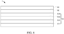
FIG. 6 is a schematic structural view illustrating the thin film encapsulation layer according to a third embodiment. - The technical solutions of the present application will be clearly and completely described below with reference to the accompanying drawings and embodiments of the present application. Obviously, the described embodiments are only some embodiments of the present application, but not all the embodiments. Based on the embodiments in the present application, all other embodiments obtained by those skilled in the art without creative work fall into the protection scope of the present application.
- In the present invention, unless otherwise clearly specified and defined, a first element being "above" or "below" a second element can indicate that the first and second elements are in direct contact with each other, or the first and second elements are not in direct contact but are in contact with another element between them. Moreover, the first element being "above", "over", or "on" the second element can indicate that the first element is right above or obliquely over the second element, or simply means that the first element is disposed at a higher level than the second element. The first element being "under", "below", or "beneath" the second element can indicate that the first element is right under and obliquely below the second element, or simply means that the first element is disposed at a lower level than the second element.
- In the present invention, the same or corresponding components are denoted by the same reference numerals regardless of the figure number. In the whole specification, wording like "first" and "second" can be used to describe various components; however, these components are not limited by the above wording. The above wording is only used to distinguish one component from another.
- As shown in
FIG. 1 , aflexible display panel 100 is provided according to the first embodiment of the present invention. Theflexible display panel 100 comprises anarray substrate 1, an organic light-emitting layer 2, acathode layer 3, an opticalcoupling output layer 4, and a thinfilm encapsulation layer 5. Thearray substrate 1 is provided with ananode layer 111. The organic light-emittinglayer 2 is disposed on theanode layer 111 and comprises ared pixel unit 201, agreen pixel unit 202, and ablue pixel unit 203. Thecathode layer 3 is disposed on the organic light-emittinglayer 2. The opticalcoupling output layer 4 is disposed on thecathode layer 3 and arranged corresponding to thered pixel unit 201 and thegreen pixel unit 202 of the organic light-emittinglayer 2. The thinfilm encapsulation layer 5 is disposed on the opticalcoupling output layer 4. The thinfilm encapsulation layer 5 corresponding to theblue pixel unit 203 of the organic light-emittinglayer 2 is in contact with thecathode layer 3. - In the present embodiment, the optical
coupling output layer 4 is produced by evaporation deposition or by printing a small molecule organic material. The opticalcoupling output layer 4 is disposed on the cathode layer and arranged only in positions corresponding to thered pixel unit 201 and thegreen pixel unit 202 of the organic light-emittinglayer 2, not in positions corresponding to theblue pixel unit 3. - Referring to
FIGs. 1 and2 , in the present embodiment, the thinfilm encapsulation layer 5 comprises a firstinorganic barrier layer 51, anorganic barrier layer 52, and a secondinorganic barrier layer 53. The firstinorganic barrier layer 51 is disposed on the opticalcoupling output layer 4 and thecathode layer 3 corresponding to theblue pixel unit 203. Theorganic barrier layer 52 is disposed on the firstinorganic barrier layer 51. The secondinorganic barrier layer 53 is disposed on theorganic barrier layer 52. - Referring to
FIG. 2 , in the present embodiment, the firstinorganic barrier layer 51 comprises a firstinorganic layer 511 and a secondinorganic layer 512. The firstinorganic layer 511 has a refractive index greater than or equal to 1.76 and less than or equal to 2. The secondinorganic layer 512 is disposed on the firstinorganic layer 511, a water vapor transmission rate (WVTR) of the secondinorganic layer 512 is less than 1 × 10⁻⁴ g / (m2 · 24h). The firstinorganic layer 511 has a high refractive index, which can improve light output efficiency. - In the present embodiment, material of the first
inorganic layer 511 comprises any one of SiNx, SiONx, TiOx, or ZnOx, wherein the material is preferably SiNx. - In the present embodiment, material of the second
inorganic layer 512 comprises any one of SiNx, SiONx, SiOx, Al2O3, TiOx, ZrO2, or ZnOx, wherein the material is preferably SiONx. - Referring to
FIG. 3 , in the present embodiment, thearray substrate 11 includes a flexiblebase substrate layer 101, abuffer layer 102, anactive layer 103, a firstgate insulating layer 104, afirst gate layer 105, a secondgate insulating layer 106, asecond gate layer 107, aninterlayer insulating layer 108, a source/drain layer 109, anorganic planarization layer 110, and theanode layer 111. Material of the flexiblebase substrate layer 101 is polyimide (PI). Thebuffer layer 102, the firstgate insulating layer 104, the secondgate insulating layer 106, theinterlayer insulating layer 108 are stacked inorganic layers composed of, for example, SiN/SiOx. Theactive layer 103 is a low-temperature polysilicon layer composed of low-temperature polysilicon. Material of thefirst gate layer 105 and thesecond gate layer 107 includes Mo. The source/drain layer 109 has a stacked structure of Ti/Al/Ti, and material of theorganic planarization layer 110 includes polyimide, and theanode layer 111 has a stacked structure of ITO/Ag/ITO or IZO/Ag/IZO. - Referring to
FIG. 4 , in the present embodiment, the organic light-emittinglayer 2 includes a hole injection layer 21 (HIL), a hole transport layer 22 (HTL), an organic light-emitting layer 23 (EML), an electron transport layer 24 (ETL), and an electron injection layer 25 (EIL)stacked sequentially from bottom to top. Thecathode layer 3 is disposed on theelectron injection layer 25. - As shown in
FIG. 5 , the second embodiment includes all the technical features of the first embodiment. The difference is that the firstinorganic barrier layer 51 in the second embodiment further includes a thirdinorganic layer 513 disposed between the firstinorganic layer 511 and the secondinorganic layer 512. A refractive index of the thirdinorganic layer 513 is less than or equal to 1.55. - In the present embodiment, material of the third
inorganic layer 513 includes SiOx, SiONx, or organic aluminide (Alucone), wherein the material is preferably SiOx. By means of having the thirdinorganic layer 513, water and oxygen can be better blocked. - As shown in
FIG. 6 , the third embodiment includes all the technical features of the second embodiment. The difference is that the firstinorganic barrier layer 51 in the third embodiment further includes a fourthinorganic layer 514 disposed on the secondinorganic layer 512. A refractive index of the fourthinorganic layer 514 is less than or equal to 1.55. - In the present embodiment, material of the fourth
inorganic layer 514 includes SiOx or SiONx, wherein the material is preferably SiONx. By means of having the fourthinorganic layer 514, water and oxygen can be better blocked. - The present invention has the following advantages. The present invention provides the
flexible display panel 100. The opticalcoupling output layer 4 is not arranged at a position corresponding to theblue pixel unit 203, so power consumption is reduced, and a service life of theflexible display panel 100 is also prolonged. The firstinorganic barrier layer 51 of the thinfilm encapsulation layer 5 completely replaces the opticalcoupling output layer 4 at the position corresponding to theblue pixel unit 203. Therefore, the present invention can not only maximize the efficiency of red and green light, but also effectively improve the efficiency of blue light at the same time. Meanwhile, this can also simplify an evaporation process and reduce production costs. - The above is only the preferable embodiment of the present invention. It should be noted that, for those of ordinary skill in the art, changes and modifications can be made based on the working principles of the present invention. Such changes and modifications should be deemed to be within the protection scope of the present invention.
Claims (10)
- A flexible display panel, comprising:an array substrate;an organic light-emitting layer disposed on the array substrate and comprising a red pixel unit, a green pixel unit, and a blue pixel unit;a cathode layer disposed on the organic light-emitting layer;an optical coupling output layer disposed on the cathode layer and arranged corresponding to the red pixel unit and the green pixel unit of the organic light-emitting layer; anda thin film encapsulation layer disposed on the optical coupling output layer, wherein the thin film encapsulation layer corresponding to the blue pixel unit of the organic light-emitting layer is in contact with the cathode layer.
- The flexible display panel according to claim 1, wherein the optical coupling output layer is produced by evaporation deposition or by printing a small molecule organic material.
- The flexible display panel according to claim 1, wherein the thin film encapsulation layer comprises:a first inorganic barrier layer disposed on the optical coupling output layer and the cathode layer corresponding to the blue pixel unit;an organic barrier layer disposed on the first inorganic barrier layer; anda second inorganic barrier layer disposed on the organic barrier layer.
- The flexible display panel according to claim 3, wherein the first inorganic barrier layer comprises:a first inorganic layer with a refractive index greater than or equal to 1.76 and less than or equal to 2; anda second inorganic layer disposed on the first inorganic layer, a water vapor transmission rate of the second inorganic layer is less than 1 × 10⁻⁴ g / (m2 · 24h).
- The flexible display panel according to claim 4, wherein material of the first inorganic layer comprises any one of SiNx, SiONx, TiOx, or ZnOx.
- The flexible display panel according to claim 4, wherein material of the second inorganic layer comprises any one of SiNx, SiONx, SiOx, Al2O3, TiOx, ZrO2, or ZnOx.
- The flexible display panel according to claim 4, wherein the first inorganic barrier layer comprises:
a third inorganic layer disposed between the first inorganic layer and the second inorganic layer, and a refractive index of the third inorganic layer is less than or equal to 1.55. - The flexible display panel according to claim 7, wherein material of the third inorganic layer comprises SiOx, SiONx, or organic aluminide.
- The flexible display panel according to claim 4, wherein the first inorganic barrier layer comprises:
a fourth inorganic layer disposed on the second inorganic layer, and a refractive index of the fourth inorganic layer is less than or equal to 1.55. - The flexible display panel according to claim 9, wherein material of the fourth inorganic layer comprises SiOx or SiONx.
Applications Claiming Priority (2)
| Application Number | Priority Date | Filing Date | Title |
|---|---|---|---|
| CN202010111845.3A CN111293232B (en) | 2020-02-24 | 2020-02-24 | Flexible display panel |
| PCT/CN2020/083082 WO2021168992A1 (en) | 2020-02-24 | 2020-04-02 | Flexible display panel |
Publications (2)
| Publication Number | Publication Date |
|---|---|
| EP4113640A1 true EP4113640A1 (en) | 2023-01-04 |
| EP4113640A4 EP4113640A4 (en) | 2024-04-17 |
Family
ID=71020472
Family Applications (1)
| Application Number | Title | Priority Date | Filing Date |
|---|---|---|---|
| EP20767708.9A Pending EP4113640A4 (en) | 2020-02-24 | 2020-04-02 | Flexible display panel |
Country Status (4)
| Country | Link |
|---|---|
| US (1) | US11903259B2 (en) |
| EP (1) | EP4113640A4 (en) |
| CN (1) | CN111293232B (en) |
| WO (1) | WO2021168992A1 (en) |
Family Cites Families (14)
| Publication number | Priority date | Publication date | Assignee | Title |
|---|---|---|---|---|
| CN103165680B (en) * | 2013-03-07 | 2016-04-20 | 北京京东方光电科技有限公司 | A kind of substrate for display and display unit |
| KR20160083986A (en) * | 2015-01-02 | 2016-07-13 | 삼성디스플레이 주식회사 | Organic light emitting diode device |
| KR102424966B1 (en) * | 2015-02-13 | 2022-07-26 | 삼성디스플레이 주식회사 | Organic light emitting diode device |
| CN107180847B (en) * | 2016-03-18 | 2021-04-20 | 京东方科技集团股份有限公司 | Pixel structure, organic light-emitting display panel and method of making the same, and display device |
| JP6817807B2 (en) * | 2016-12-22 | 2021-01-20 | 株式会社ジャパンディスプレイ | Display device |
| CN106684256A (en) | 2016-12-23 | 2017-05-17 | 上海天马有机发光显示技术有限公司 | Display panel and fabrication method thereof |
| CN107359266A (en) | 2017-04-21 | 2017-11-17 | 瑞声科技(新加坡)有限公司 | OLED composite barrier films, and the display using the OLED composite barrier films |
| CN107123751B (en) | 2017-04-28 | 2019-04-16 | 武汉华星光电技术有限公司 | A kind of flexible organic light emitting diode display and preparation method thereof |
| US10658441B2 (en) * | 2017-08-28 | 2020-05-19 | Apple Inc. | Organic light-emitting diode displays with reflectors |
| CN107565038B (en) * | 2017-08-29 | 2019-09-24 | 上海天马微电子有限公司 | Display panel and display device |
| JP6994914B2 (en) * | 2017-11-21 | 2022-01-14 | 株式会社ジャパンディスプレイ | Organic EL display device |
| CN109686864A (en) | 2019-01-23 | 2019-04-26 | 武汉华星光电半导体显示技术有限公司 | Organic light emitting apparatus, display device |
| CN110649078B (en) | 2019-09-30 | 2022-01-11 | 京东方科技集团股份有限公司 | Substrate for display and display device |
| CN110707146B (en) | 2019-11-22 | 2022-09-09 | 京东方科技集团股份有限公司 | Cover plate, organic light-emitting display panel, display device |
-
2020
- 2020-02-24 CN CN202010111845.3A patent/CN111293232B/en active Active
- 2020-04-02 EP EP20767708.9A patent/EP4113640A4/en active Pending
- 2020-04-02 US US16/966,035 patent/US11903259B2/en active Active
- 2020-04-02 WO PCT/CN2020/083082 patent/WO2021168992A1/en not_active Ceased
Also Published As
| Publication number | Publication date |
|---|---|
| US11903259B2 (en) | 2024-02-13 |
| US20230157078A1 (en) | 2023-05-18 |
| CN111293232B (en) | 2021-06-25 |
| CN111293232A (en) | 2020-06-16 |
| WO2021168992A1 (en) | 2021-09-02 |
| EP4113640A4 (en) | 2024-04-17 |
Similar Documents
| Publication | Publication Date | Title |
|---|---|---|
| US10535719B2 (en) | Color film substrate for WOLED display and WOLED display | |
| CN106654046B (en) | OLED display panel and preparation method thereof | |
| US9595691B2 (en) | Organic light emitting diode device | |
| WO2018113018A1 (en) | Oled display panel and manufacturing method therefor | |
| KR101084243B1 (en) | Organic light emitting display | |
| US20210273196A1 (en) | Oled display panel | |
| US9705104B2 (en) | OLED display substrate and manufacture method thereof | |
| KR101065404B1 (en) | Organic light emitting display | |
| WO2016058531A1 (en) | Organic light-emitting diode and preparation method therefor, display substrate and display device | |
| CN106783924B (en) | OLED display panel and manufacturing method thereof | |
| CN103000660B (en) | Array substrate and white organic light-emitting diode display device | |
| KR20170084736A (en) | Display apparatus | |
| CN103413898B (en) | Organic Light Emitting Diode anode syndeton and preparation method thereof | |
| US8686443B2 (en) | Organic light-emitting display device | |
| US20210336236A1 (en) | Display panel and manufacturing method thereof | |
| US11903259B2 (en) | Flexible display panel | |
| US9159775B1 (en) | Anode connection structure of organic light-emitting diode and manufacturing method thereof | |
| CN104752463B (en) | A kind of organic light-emitting display device and preparation method thereof | |
| US11152588B2 (en) | OLED light emitting device and OLED display device having a smoothing layer | |
| EP3706186A1 (en) | Manufacturing method of oled substrate and manufacturing method of oled display device | |
| US20250221158A1 (en) | Display device | |
| KR101528923B1 (en) | Organic light-emitting diode display element and its manufacturing method | |
| US20180294318A1 (en) | Organic electroluminescence device and manufacturing method for the same | |
| KR20100010177A (en) | Organic light emitting display and manufacturing method for the same |
Legal Events
| Date | Code | Title | Description |
|---|---|---|---|
| STAA | Information on the status of an ep patent application or granted ep patent |
Free format text: STATUS: UNKNOWN |
|
| STAA | Information on the status of an ep patent application or granted ep patent |
Free format text: STATUS: THE INTERNATIONAL PUBLICATION HAS BEEN MADE |
|
| PUAI | Public reference made under article 153(3) epc to a published international application that has entered the european phase |
Free format text: ORIGINAL CODE: 0009012 |
|
| STAA | Information on the status of an ep patent application or granted ep patent |
Free format text: STATUS: REQUEST FOR EXAMINATION WAS MADE |
|
| 17P | Request for examination filed |
Effective date: 20200915 |
|
| AK | Designated contracting states |
Kind code of ref document: A1 Designated state(s): AL AT BE BG CH CY CZ DE DK EE ES FI FR GB GR HR HU IE IS IT LI LT LU LV MC MK MT NL NO PL PT RO RS SE SI SK SM TR |
|
| DAV | Request for validation of the european patent (deleted) | ||
| DAX | Request for extension of the european patent (deleted) | ||
| REG | Reference to a national code |
Ref country code: DE Ref legal event code: R079 Free format text: PREVIOUS MAIN CLASS: H01L0051520000 Ipc: G09F0009300000 |
|
| A4 | Supplementary search report drawn up and despatched |
Effective date: 20240319 |
|
| RIC1 | Information provided on ipc code assigned before grant |
Ipc: H10K 102/00 20230101ALI20240313BHEP Ipc: H10K 59/35 20230101ALI20240313BHEP Ipc: H10K 59/12 20230101ALI20240313BHEP Ipc: H10K 77/10 20230101ALI20240313BHEP Ipc: H10K 50/858 20230101ALI20240313BHEP Ipc: H10K 50/844 20230101ALI20240313BHEP Ipc: H10K 59/80 20230101ALI20240313BHEP Ipc: G09F 9/30 20060101AFI20240313BHEP |