EP4113593A2 - Polyimide bonded bus bar for power device - Google Patents
Polyimide bonded bus bar for power device Download PDFInfo
- Publication number
- EP4113593A2 EP4113593A2 EP22182395.8A EP22182395A EP4113593A2 EP 4113593 A2 EP4113593 A2 EP 4113593A2 EP 22182395 A EP22182395 A EP 22182395A EP 4113593 A2 EP4113593 A2 EP 4113593A2
- Authority
- EP
- European Patent Office
- Prior art keywords
- bus bar
- metal
- metal bus
- heat sink
- polyimide layer
- Prior art date
- Legal status (The legal status is an assumption and is not a legal conclusion. Google has not performed a legal analysis and makes no representation as to the accuracy of the status listed.)
- Withdrawn
Links
Images

Classifications
-
- H—ELECTRICITY
- H05—ELECTRIC TECHNIQUES NOT OTHERWISE PROVIDED FOR
- H05K—PRINTED CIRCUITS; CASINGS OR CONSTRUCTIONAL DETAILS OF ELECTRIC APPARATUS; MANUFACTURE OF ASSEMBLAGES OF ELECTRICAL COMPONENTS
- H05K7/00—Constructional details common to different types of electric apparatus
- H05K7/20—Modifications to facilitate cooling, ventilating, or heating
- H05K7/2089—Modifications to facilitate cooling, ventilating, or heating for power electronics, e.g. for inverters for controlling motor
- H05K7/209—Heat transfer by conduction from internal heat source to heat radiating structure
-
- H—ELECTRICITY
- H10—SEMICONDUCTOR DEVICES; ELECTRIC SOLID-STATE DEVICES NOT OTHERWISE PROVIDED FOR
- H10W—GENERIC PACKAGES, INTERCONNECTIONS, CONNECTORS OR OTHER CONSTRUCTIONAL DETAILS OF DEVICES COVERED BY CLASS H10
- H10W40/00—Arrangements for thermal protection or thermal control
- H10W40/10—Arrangements for heating
-
- H—ELECTRICITY
- H10—SEMICONDUCTOR DEVICES; ELECTRIC SOLID-STATE DEVICES NOT OTHERWISE PROVIDED FOR
- H10W—GENERIC PACKAGES, INTERCONNECTIONS, CONNECTORS OR OTHER CONSTRUCTIONAL DETAILS OF DEVICES COVERED BY CLASS H10
- H10W40/00—Arrangements for thermal protection or thermal control
- H10W40/20—Arrangements for cooling
- H10W40/25—Arrangements for cooling characterised by their materials
- H10W40/251—Organics
-
- H—ELECTRICITY
- H10—SEMICONDUCTOR DEVICES; ELECTRIC SOLID-STATE DEVICES NOT OTHERWISE PROVIDED FOR
- H10W—GENERIC PACKAGES, INTERCONNECTIONS, CONNECTORS OR OTHER CONSTRUCTIONAL DETAILS OF DEVICES COVERED BY CLASS H10
- H10W70/00—Package substrates; Interposers; Redistribution layers [RDL]
- H10W70/01—Manufacture or treatment
- H10W70/02—Manufacture or treatment of conductive package substrates serving as an interconnection, e.g. of metal plates
-
- H—ELECTRICITY
- H10—SEMICONDUCTOR DEVICES; ELECTRIC SOLID-STATE DEVICES NOT OTHERWISE PROVIDED FOR
- H10W—GENERIC PACKAGES, INTERCONNECTIONS, CONNECTORS OR OTHER CONSTRUCTIONAL DETAILS OF DEVICES COVERED BY CLASS H10
- H10W70/00—Package substrates; Interposers; Redistribution layers [RDL]
- H10W70/20—Conductive package substrates serving as an interconnection, e.g. metal plates
-
- H—ELECTRICITY
- H10—SEMICONDUCTOR DEVICES; ELECTRIC SOLID-STATE DEVICES NOT OTHERWISE PROVIDED FOR
- H10W—GENERIC PACKAGES, INTERCONNECTIONS, CONNECTORS OR OTHER CONSTRUCTIONAL DETAILS OF DEVICES COVERED BY CLASS H10
- H10W40/00—Arrangements for thermal protection or thermal control
- H10W40/01—Manufacture or treatment
- H10W40/03—Manufacture or treatment of arrangements for cooling
- H10W40/037—Assembling together parts thereof
-
- H—ELECTRICITY
- H10—SEMICONDUCTOR DEVICES; ELECTRIC SOLID-STATE DEVICES NOT OTHERWISE PROVIDED FOR
- H10W—GENERIC PACKAGES, INTERCONNECTIONS, CONNECTORS OR OTHER CONSTRUCTIONAL DETAILS OF DEVICES COVERED BY CLASS H10
- H10W40/00—Arrangements for thermal protection or thermal control
- H10W40/70—Fillings or auxiliary members in containers or in encapsulations for thermal protection or control
-
- H—ELECTRICITY
- H10—SEMICONDUCTOR DEVICES; ELECTRIC SOLID-STATE DEVICES NOT OTHERWISE PROVIDED FOR
- H10W—GENERIC PACKAGES, INTERCONNECTIONS, CONNECTORS OR OTHER CONSTRUCTIONAL DETAILS OF DEVICES COVERED BY CLASS H10
- H10W90/00—Package configurations
Definitions
- Exemplary embodiments pertain to the art of bus bars for semiconductor devices.
- thermal pads are installed between bus bar and heat sink. Typically more than one pad is used in order to prevent pin hole line up.
- the thermal pads are a limiting factor for device integrity and performance due to electrical, mechanical and thermal limits. Better solutions for heat and power flow separation are needed.
- a semiconductor article including: a metal bus bar and a metal heat sink wherein at least a portion of a first side of the metal bus bar is bonded to at least a portion of the metal heat sink by a polyimide layer without adhesive; and a semiconductor power device disposed on a second side of the metal bus bar.
- the first side of the metal bus bar is opposite the second side of the metal bus bar.
- the semiconductor article has a power flow direction and a heat flow direction and the power flow direction is different from the heat flow direction.
- the metal bus bar consists of a metal, a metal alloy, or a combination of metals.
- only the first side of the metal bus bar is bonded to the polyimide layer.
- the bond between the metal bus bar and polyimide layer is free of voids.
- the bond between the metal heat sink and polyimide layer is free of voids.
- the metal bus bar and the polyimide layer each have a coefficient of thermal expansion (CTE) and the polyimide layer CTE is 90-110% of the metal bus bar CTE.
- CTE coefficient of thermal expansion
- the metal heat sink and the polyimide layer each have a coefficient of thermal expansion (CTE) and the polyimide layer CTE is 90-110% of the metal heat sink CTE.
- CTE coefficient of thermal expansion
- the semiconductor article may further include an additional semiconductor device disposed on a side of the metal bus bar other than the first side.
- the metal bus bar comprises aluminum or an aluminum alloy.
- the semiconductor article further includes an additional metal bus bar having at least a portion of a first side of the additional metal bus bar bonded to at least a portion of the metal heat sink by the polyimide layer or an additional polyimide layer and an additional semiconductor power device disposed on a second side of the additional metal bus bar.
- the method includes including bonding a metal bus bar to a metal heat sink by locating a polyimide layer between at least a portion of a first side of the metal bus bar and at least a portion of the metal heat sink to form a stack without adhesive and heating the stack to bond the stack; and disposing a semiconductor power device on a second side of the metal bus bar.
- the stack is heated to a temperature of 380°C to 420°C.
- the metal bus bar comprises aluminum or an aluminum alloy.
- the stack is heated to a temperature above the glass transition temperature of the polyimide and below the degradation temperature of the polyimide.
- FIG. 1 shows a semiconductor article 100 having a first side of metal bus bar 15 bonded to metal heat sink 40 by polyimide layer 30.
- Semiconductor device 10 is located on bus bar 15. Power flows through the metal bus bar in a direction different from the direction of the heat flow in the metal heat sink.
- the polyimide layer 30 is bonded to the metal bus bar 15 and metal heat sink without adhesive.
- the bond to the metal bus bar and to the metal heat sink is effected by using heat and optionally pressure.
- air pockets (voids) are eliminated which makes the resulting bus bar more reliable, consistent and robust.
- the metal bus bar may be a metal, a metal alloy or a combination of metals. Exemplary metals and metal alloys include aluminum and aluminum alloys.
- the metal bus bar may have a similar coefficient of thermal expansion to the polyimide layer. In some embodiments, the polyimide layer coefficient of thermal expansion is 90 to 110% of the metal bus bar coefficient of thermal expansion.
- the metal heat sink may be a metal, a metal alloy or a combination of metals. Exemplary metals and metal alloys include aluminum and aluminum alloys.
- the metal heat sink may have a similar coefficient of thermal expansion to the polyimide layer. In some embodiments, the polyimide layer coefficient of thermal expansion is 90 to 110% of the metal heat sink coefficient of thermal expansion.
- the metal bus bar is bonded to the metal heat sink by locating the polyimide layer between the metal bus bar and the metal heat sink to form a stack and then subjecting the stack to a temperature that is greater than the glass transition temperature of the polyimide and less than the degradation temperature of the polyimide. Representative temperatures are 380°C to 420°C. While at that temperature, the stack may be subjected to an elevated pressure (greater than atmospheric pressure). The stack may be subjected to the elevated temperature for a time sufficient to result in bonding, more specifically for a time sufficient to allow the polyimide at the surface of the metal bus bar and the metal heat sink to flow into the surface structure of the metal bus bar and the metal heat sink, thus forming a bond without voids.
- a semiconductor device such as a semiconductor power device is attached to the metal bus bar using an appropriate attachment means such as a threaded fastener.
- Bonding the polyimide portion to the metal portion facilitates fabrication of the semiconductor article as there is no need to locate a separate thermal pad or multiple thermal pads between the bus bar and heat sink. Additionally, semiconductor article produced as described above has more resilience to temperature cycling and a higher operating temperature. The higher operating temperature improves the power density of the device.
- Semiconductor device 10 may be a semiconductor power device or any other semiconductor device without limitation.
- the semiconductor device includes at least one semiconductor chip and may further include one or more circuit boards including insulating circuit boards and printed circuit boards.
- Examples of semiconductor chips include a switching element such as insulated gate bipolar transistor (IGBT), and a power metal oxide semiconductor field effect transistor (power MOSFET) and a diode such as a freewheeling diode (FWD).
- IGBT insulated gate bipolar transistor
- power MOSFET power metal oxide semiconductor field effect transistor
- FWD freewheeling diode
- elements such as a reverse conducting (RC)-IGBT, including integrated IGBT and FWD, and reverse blocking (RB)-IGBT may be used.
- RC reverse conducting
- RB reverse blocking
- the semiconductor article is not limited to a single semiconductor device, a single bus bar and a single heat sink.
- FIG. 1 shows a single semiconductor device, a single bus bar and a single heat sink for simplicity.
- Other configurations are contemplated such as those shown in FIGS. 2 and 3 which have two semiconductor devices and two bus bars but only one heat sink. Any combination of semiconductor devices, bus bars and heat sinks may be used.
Landscapes
- Engineering & Computer Science (AREA)
- Microelectronics & Electronic Packaging (AREA)
- Physics & Mathematics (AREA)
- Thermal Sciences (AREA)
- Cooling Or The Like Of Semiconductors Or Solid State Devices (AREA)
- Chemical & Material Sciences (AREA)
- Materials Engineering (AREA)
- Die Bonding (AREA)
Abstract
Description
- Exemplary embodiments pertain to the art of bus bars for semiconductor devices.
- Heat and power flow separation in semiconductor devices is frequently achieved through the use of thermal pads. These pads are installed between bus bar and heat sink. Typically more than one pad is used in order to prevent pin hole line up. The thermal pads are a limiting factor for device integrity and performance due to electrical, mechanical and thermal limits. Better solutions for heat and power flow separation are needed.
- Disclosed is a semiconductor article including: a metal bus bar and a metal heat sink wherein at least a portion of a first side of the metal bus bar is bonded to at least a portion of the metal heat sink by a polyimide layer without adhesive; and a semiconductor power device disposed on a second side of the metal bus bar.
- In embodiments, the first side of the metal bus bar is opposite the second side of the metal bus bar.
- In embodiments, the semiconductor article has a power flow direction and a heat flow direction and the power flow direction is different from the heat flow direction.
- In embodiments, the metal bus bar consists of a metal, a metal alloy, or a combination of metals.
- In embodiments, only the first side of the metal bus bar is bonded to the polyimide layer.
- In embodiments, the bond between the metal bus bar and polyimide layer is free of voids.
- In embodiments, the bond between the metal heat sink and polyimide layer is free of voids.
- In embodiments, the metal bus bar and the polyimide layer each have a coefficient of thermal expansion (CTE) and the polyimide layer CTE is 90-110% of the metal bus bar CTE.
- In embodiments, the metal heat sink and the polyimide layer each have a coefficient of thermal expansion (CTE) and the polyimide layer CTE is 90-110% of the metal heat sink CTE.
- In embodiments, the semiconductor article may further include an additional semiconductor device disposed on a side of the metal bus bar other than the first side.
- In embodiments, the metal bus bar comprises aluminum or an aluminum alloy.
- In embodiments, the semiconductor article further includes an additional metal bus bar having at least a portion of a first side of the additional metal bus bar bonded to at least a portion of the metal heat sink by the polyimide layer or an additional polyimide layer and an additional semiconductor power device disposed on a second side of the additional metal bus bar.
- Also disclosed is a method of making a semiconductor article. The method includes including bonding a metal bus bar to a metal heat sink by locating a polyimide layer between at least a portion of a first side of the metal bus bar and at least a portion of the metal heat sink to form a stack without adhesive and heating the stack to bond the stack; and disposing a semiconductor power device on a second side of the metal bus bar.
- In embodiments, the stack is heated to a temperature of 380°C to 420°C.
- In embodiments, the metal bus bar comprises aluminum or an aluminum alloy.
- In embodiments, the stack is heated to a temperature above the glass transition temperature of the polyimide and below the degradation temperature of the polyimide.
- The following descriptions should not be considered limiting in any way. With reference to the accompanying drawings, like elements are numbered alike:
-
FIG. 1 shows a semiconductor article with a single semiconductor device; -
FIG. 2 shows an embodiment of a semiconductor article with two bus bars and two semiconductor devices; and -
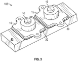
FIG. 3 shows another embodiment of a semiconductor article with two bus bars and two semiconductor devices. - A detailed description of one or more embodiments of the disclosed apparatus and method are presented herein by way of exemplification and not limitation with reference to the Figures.
-
FIG. 1 shows asemiconductor article 100 having a first side ofmetal bus bar 15 bonded tometal heat sink 40 bypolyimide layer 30.Semiconductor device 10 is located onbus bar 15. Power flows through the metal bus bar in a direction different from the direction of the heat flow in the metal heat sink. - The
polyimide layer 30 is bonded to themetal bus bar 15 and metal heat sink without adhesive. The bond to the metal bus bar and to the metal heat sink is effected by using heat and optionally pressure. By bonding the polyimide to the metal bus bar and metal heat sink under these conditions air pockets (voids) are eliminated which makes the resulting bus bar more reliable, consistent and robust. The metal bus bar may be a metal, a metal alloy or a combination of metals. Exemplary metals and metal alloys include aluminum and aluminum alloys. The metal bus bar may have a similar coefficient of thermal expansion to the polyimide layer. In some embodiments, the polyimide layer coefficient of thermal expansion is 90 to 110% of the metal bus bar coefficient of thermal expansion. - The metal heat sink may be a metal, a metal alloy or a combination of metals. Exemplary metals and metal alloys include aluminum and aluminum alloys. The metal heat sink may have a similar coefficient of thermal expansion to the polyimide layer. In some embodiments, the polyimide layer coefficient of thermal expansion is 90 to 110% of the metal heat sink coefficient of thermal expansion.
- The metal bus bar is bonded to the metal heat sink by locating the polyimide layer between the metal bus bar and the metal heat sink to form a stack and then subjecting the stack to a temperature that is greater than the glass transition temperature of the polyimide and less than the degradation temperature of the polyimide. Representative temperatures are 380°C to 420°C. While at that temperature, the stack may be subjected to an elevated pressure (greater than atmospheric pressure). The stack may be subjected to the elevated temperature for a time sufficient to result in bonding, more specifically for a time sufficient to allow the polyimide at the surface of the metal bus bar and the metal heat sink to flow into the surface structure of the metal bus bar and the metal heat sink, thus forming a bond without voids. After the metal bus bar and the metal heat sink have been bonded a semiconductor device such as a semiconductor power device is attached to the metal bus bar using an appropriate attachment means such as a threaded fastener.
- Bonding the polyimide portion to the metal portion facilitates fabrication of the semiconductor article as there is no need to locate a separate thermal pad or multiple thermal pads between the bus bar and heat sink. Additionally, semiconductor article produced as described above has more resilience to temperature cycling and a higher operating temperature. The higher operating temperature improves the power density of the device.
-
Semiconductor device 10 may be a semiconductor power device or any other semiconductor device without limitation. The semiconductor device includes at least one semiconductor chip and may further include one or more circuit boards including insulating circuit boards and printed circuit boards. Examples of semiconductor chips include a switching element such as insulated gate bipolar transistor (IGBT), and a power metal oxide semiconductor field effect transistor (power MOSFET) and a diode such as a freewheeling diode (FWD). Also, elements such as a reverse conducting (RC)-IGBT, including integrated IGBT and FWD, and reverse blocking (RB)-IGBT may be used. - The semiconductor article is not limited to a single semiconductor device, a single bus bar and a single heat sink.
FIG. 1 shows a single semiconductor device, a single bus bar and a single heat sink for simplicity. Other configurations are contemplated such as those shown inFIGS. 2 and3 which have two semiconductor devices and two bus bars but only one heat sink. Any combination of semiconductor devices, bus bars and heat sinks may be used. - The terminology used herein is for the purpose of describing particular embodiments only and is not intended to be limiting of the present disclosure. As used herein, the singular forms "a", "an" and "the" are intended to include the plural forms as well, unless the context clearly indicates otherwise. It will be further understood that the terms "comprises" and/or "comprising," when used in this specification, specify the presence of stated features, integers, steps, operations, elements, and/or components, but do not preclude the presence or addition of one or more other features, integers, steps, operations, element components, and/or groups thereof. The terms "comprises" and/or "comprising" as well as "includes" and/or "including" includes "consists of and/or "consisting of."
- While the present disclosure has been described with reference to an exemplary embodiment or embodiments, it will be understood by those skilled in the art that various changes may be made without departing from the scope of the invention as defined by the claims. In addition, many modifications may be made to adapt a particular situation or material to the teachings of the present disclosure without departing from the scope of the claims . Therefore, it is intended that the present disclosure not be limited to the particular embodiment disclosed as the best mode contemplated for carrying out this present disclosure, but that the present disclosure will include all embodiments falling within the scope of the claims.
Claims (15)
- A semiconductor article comprising a metal bus bar (15) and a metal heat sink (40) wherein at least a portion of a first side of the metal bus bar is bonded to at least a portion of the metal heat sink by a polyimide layer without adhesive; and a semiconductor power device (10) disposed on a second side of the metal bus bar.
- The semiconductor article of claim 1, wherein the first side of the metal bus bar (15) is opposite the second side of the metal bus bar.
- The semiconductor article of claim 1 or 2, wherein the semiconductor article (100) has a power flow direction and a heat flow direction and the power flow direction is different from the heat flow direction.
- The semiconductor article of any preceding claim, wherein the metal bus bar consists of a metal, a metal alloy or a combination of metals.
- The semiconductor article of any preceding claim, wherein only the first side of the metal bus bar is bonded to the polyimide layer.
- The semiconductor article of any preceding claim, wherein the bond between the metal bus bar and polyimide layer is free of voids.
- The semiconductor article of any preceding claim, wherein the bond between the metal heat sink and polyimide layer is free of voids.
- The semiconductor article of any preceding claim , wherein the metal bus bar and the polyimide layer each have a coefficient of thermal expansion, CTE, and the polyimide layer CTE is 90-110% of the metal bus bar CTE.
- The semiconductor article of any of claims 1 to 7 wherein the metal heat sink and the polyimide layer each have a coefficient of thermal expansion, CTE, and the polyimide layer CTE is 90-110% of the metal heat sink CTE.
- The semiconductor article of any preceding claim , further comprising at least a portion of a first side of an additional metal bus bar bonded to at least a portion of the metal heat sink by an additional polyimide layer without adhesive; and an additional semiconductor power device disposed on a second side of the additional metal bus bar.
- The semiconductor article of any preceding claim , wherein the metal bus bar comprises aluminum or an aluminum alloy.
- A method of making a semiconductor article comprising:bonding a metal bus bar (15) to a metal heat sink (40) by locating a polyimide layer between at least a portion of a first side of the metal bus bar and at least a portion of the metal heat sink to form a stack without adhesive and heating the stack to bond the stack; anddisposing a semiconductor power device (10) on a second side of the metal bus bar.
- The method of claim 12, wherein the stack is heated to a temperature of 380°C to 420°C.
- The method of claim 12 or 13, wherein the metal bus bar comprises aluminum or an aluminum alloy.
- The method of claim 12, 13 or 14, wherein the stack is heated to a temperature above the glass transition temperature of the polyimide and below the degradation temperature of the polyimide.
Applications Claiming Priority (1)
| Application Number | Priority Date | Filing Date | Title |
|---|---|---|---|
| US17/365,048 US20230005822A1 (en) | 2021-07-01 | 2021-07-01 | Polyimide bonded bus bar for power device |
Publications (2)
| Publication Number | Publication Date |
|---|---|
| EP4113593A2 true EP4113593A2 (en) | 2023-01-04 |
| EP4113593A3 EP4113593A3 (en) | 2023-01-11 |
Family
ID=82494053
Family Applications (1)
| Application Number | Title | Priority Date | Filing Date |
|---|---|---|---|
| EP22182395.8A Withdrawn EP4113593A3 (en) | 2021-07-01 | 2022-06-30 | Polyimide bonded bus bar for power device |
Country Status (2)
| Country | Link |
|---|---|
| US (1) | US20230005822A1 (en) |
| EP (1) | EP4113593A3 (en) |
Family Cites Families (6)
| Publication number | Priority date | Publication date | Assignee | Title |
|---|---|---|---|---|
| JPS61163938A (en) * | 1985-01-15 | 1986-07-24 | Matsushita Electric Works Ltd | Addition-type imide resin prepolymer, prepreg and laminated sheet |
| US5145553A (en) * | 1991-05-06 | 1992-09-08 | International Business Machines Corporation | Method of making a flexible circuit member |
| JP3198796B2 (en) * | 1993-06-25 | 2001-08-13 | 富士電機株式会社 | Mold module |
| JP5936310B2 (en) * | 2011-03-17 | 2016-06-22 | 三菱電機株式会社 | Power semiconductor module and its mounting structure |
| JP6094044B2 (en) * | 2011-03-23 | 2017-03-15 | 大日本印刷株式会社 | Heat dissipation board and element using the same |
| KR101963271B1 (en) * | 2014-01-28 | 2019-07-31 | 삼성전기주식회사 | Power module package and the method of manufacturing thereof |
-
2021
- 2021-07-01 US US17/365,048 patent/US20230005822A1/en not_active Abandoned
-
2022
- 2022-06-30 EP EP22182395.8A patent/EP4113593A3/en not_active Withdrawn
Also Published As
| Publication number | Publication date |
|---|---|
| US20230005822A1 (en) | 2023-01-05 |
| EP4113593A3 (en) | 2023-01-11 |
Similar Documents
| Publication | Publication Date | Title |
|---|---|---|
| US6992887B2 (en) | Liquid cooled semiconductor device | |
| US10117323B2 (en) | Circuit board with a heat-conducting element | |
| CN104103608B (en) | high power single-die semiconductor package | |
| US10236231B2 (en) | Semiconductor device | |
| US20190006260A1 (en) | Molded package with chip carrier comprising brazed electrically conductive layers | |
| KR100957078B1 (en) | Electrically Isolated Power Device Package | |
| JP5125241B2 (en) | Power module substrate manufacturing method | |
| US20160056088A1 (en) | Cold Plate, Device Comprising a Cold Plate and Method for Fabricating a Cold Plate | |
| US11665813B2 (en) | Power electronics cooling assemblies and methods for making the same | |
| US10109556B2 (en) | Systems and methods for spring-based device attachment | |
| US10643917B2 (en) | Magnetic phase change material for heat dissipation | |
| TWI295837B (en) | Multi lead frame power package | |
| US20180174987A1 (en) | Semiconductor device | |
| JP6860334B2 (en) | Semiconductor device | |
| CN100385652C (en) | Semiconductor device with a plurality of semiconductor chips | |
| US7190068B2 (en) | Bottom heat spreader | |
| CN111244061B (en) | Packaging structure of GaN devices | |
| EP3410481A1 (en) | Power semiconductor chip module | |
| US20230005822A1 (en) | Polyimide bonded bus bar for power device | |
| CN111433910A (en) | Semiconductor device and method of manufacturing the same | |
| JP2016122719A (en) | Method for manufacturing semiconductor module | |
| US20200266122A1 (en) | Electronic Chip Reliably Mounted with Compressive Strain | |
| CN104867897A (en) | Diode power module | |
| WO2004112131A1 (en) | Semiconductor device | |
| CN114615857A (en) | Heat dissipation for power switches |
Legal Events
| Date | Code | Title | Description |
|---|---|---|---|
| PUAI | Public reference made under article 153(3) epc to a published international application that has entered the european phase |
Free format text: ORIGINAL CODE: 0009012 |
|
| STAA | Information on the status of an ep patent application or granted ep patent |
Free format text: STATUS: THE APPLICATION HAS BEEN PUBLISHED |
|
| PUAL | Search report despatched |
Free format text: ORIGINAL CODE: 0009013 |
|
| AK | Designated contracting states |
Kind code of ref document: A2 Designated state(s): AL AT BE BG CH CY CZ DE DK EE ES FI FR GB GR HR HU IE IS IT LI LT LU LV MC MK MT NL NO PL PT RO RS SE SI SK SM TR |
|
| AK | Designated contracting states |
Kind code of ref document: A3 Designated state(s): AL AT BE BG CH CY CZ DE DK EE ES FI FR GB GR HR HU IE IS IT LI LT LU LV MC MK MT NL NO PL PT RO RS SE SI SK SM TR |
|
| RIC1 | Information provided on ipc code assigned before grant |
Ipc: H01L 23/32 20060101ALI20221202BHEP Ipc: H01L 23/36 20060101AFI20221202BHEP |
|
| STAA | Information on the status of an ep patent application or granted ep patent |
Free format text: STATUS: THE APPLICATION IS DEEMED TO BE WITHDRAWN |
|
| 18D | Application deemed to be withdrawn |
Effective date: 20230712 |