EP4113177B1 - Metamaterialstruktur - Google Patents
Metamaterialstruktur Download PDFInfo
- Publication number
- EP4113177B1 EP4113177B1 EP22174540.9A EP22174540A EP4113177B1 EP 4113177 B1 EP4113177 B1 EP 4113177B1 EP 22174540 A EP22174540 A EP 22174540A EP 4113177 B1 EP4113177 B1 EP 4113177B1
- Authority
- EP
- European Patent Office
- Prior art keywords
- nanostructures
- angle
- nanostructure
- peak wavelength
- pattern
- Prior art date
- Legal status (The legal status is an assumption and is not a legal conclusion. Google has not performed a legal analysis and makes no representation as to the accuracy of the status listed.)
- Active
Links
Images




Classifications
-
- B—PERFORMING OPERATIONS; TRANSPORTING
- B22—CASTING; POWDER METALLURGY
- B22F—WORKING METALLIC POWDER; MANUFACTURE OF ARTICLES FROM METALLIC POWDER; MAKING METALLIC POWDER; APPARATUS OR DEVICES SPECIALLY ADAPTED FOR METALLIC POWDER
- B22F1/00—Metallic powder; Treatment of metallic powder, e.g. to facilitate working or to improve properties
- B22F1/05—Metallic powder characterised by the size or surface area of the particles
- B22F1/054—Nanosized particles
- B22F1/0553—Complex form nanoparticles, e.g. prism, pyramid, octahedron
-
- A—HUMAN NECESSITIES
- A61—MEDICAL OR VETERINARY SCIENCE; HYGIENE
- A61B—DIAGNOSIS; SURGERY; IDENTIFICATION
- A61B3/00—Apparatus for testing the eyes; Instruments for examining the eyes
- A61B3/10—Objective types, i.e. instruments for examining the eyes independent of the patients' perceptions or reactions
- A61B3/16—Objective types, i.e. instruments for examining the eyes independent of the patients' perceptions or reactions for measuring intraocular pressure, e.g. tonometers
- A61B3/165—Non-contacting tonometers
-
- B—PERFORMING OPERATIONS; TRANSPORTING
- B82—NANOTECHNOLOGY
- B82Y—SPECIFIC USES OR APPLICATIONS OF NANOSTRUCTURES; MEASUREMENT OR ANALYSIS OF NANOSTRUCTURES; MANUFACTURE OR TREATMENT OF NANOSTRUCTURES
- B82Y30/00—Nanotechnology for materials or surface science, e.g. nanocomposites
-
- B—PERFORMING OPERATIONS; TRANSPORTING
- B82—NANOTECHNOLOGY
- B82Y—SPECIFIC USES OR APPLICATIONS OF NANOSTRUCTURES; MEASUREMENT OR ANALYSIS OF NANOSTRUCTURES; MANUFACTURE OR TREATMENT OF NANOSTRUCTURES
- B82Y40/00—Manufacture or treatment of nanostructures
-
- C—CHEMISTRY; METALLURGY
- C01—INORGANIC CHEMISTRY
- C01G—COMPOUNDS CONTAINING METALS NOT COVERED BY SUBCLASSES C01D OR C01F
- C01G19/00—Compounds of tin
- C01G19/02—Oxides
-
- C—CHEMISTRY; METALLURGY
- C01—INORGANIC CHEMISTRY
- C01G—COMPOUNDS CONTAINING METALS NOT COVERED BY SUBCLASSES C01D OR C01F
- C01G28/00—Compounds of arsenic
- C01G28/002—Compounds containing arsenic, with or without oxygen or hydrogen, and containing two or more other elements
-
- C—CHEMISTRY; METALLURGY
- C01—INORGANIC CHEMISTRY
- C01G—COMPOUNDS CONTAINING METALS NOT COVERED BY SUBCLASSES C01D OR C01F
- C01G41/00—Compounds of tungsten
- C01G41/02—Oxides; Hydroxides
-
- C—CHEMISTRY; METALLURGY
- C01—INORGANIC CHEMISTRY
- C01G—COMPOUNDS CONTAINING METALS NOT COVERED BY SUBCLASSES C01D OR C01F
- C01G9/00—Compounds of zinc
- C01G9/02—Oxides; Hydroxides
-
- G—PHYSICS
- G01—MEASURING; TESTING
- G01L—MEASURING FORCE, STRESS, TORQUE, WORK, MECHANICAL POWER, MECHANICAL EFFICIENCY, OR FLUID PRESSURE
- G01L11/00—Measuring steady or quasi-steady pressure of a fluid or a fluent solid material by means not provided for in group G01L7/00 or G01L9/00
- G01L11/02—Measuring steady or quasi-steady pressure of a fluid or a fluent solid material by means not provided for in group G01L7/00 or G01L9/00 by optical means
-
- G—PHYSICS
- G02—OPTICS
- G02B—OPTICAL ELEMENTS, SYSTEMS OR APPARATUS
- G02B1/00—Optical elements characterised by the material of which they are made; Optical coatings for optical elements
- G02B1/002—Optical elements characterised by the material of which they are made; Optical coatings for optical elements made of materials engineered to provide properties not available in nature, e.g. metamaterials
-
- G—PHYSICS
- G02—OPTICS
- G02B—OPTICAL ELEMENTS, SYSTEMS OR APPARATUS
- G02B1/00—Optical elements characterised by the material of which they are made; Optical coatings for optical elements
- G02B1/10—Optical coatings produced by application to, or surface treatment of, optical elements
- G02B1/11—Anti-reflection coatings
- G02B1/118—Anti-reflection coatings having sub-optical wavelength surface structures designed to provide an enhanced transmittance, e.g. moth-eye structures
-
- G—PHYSICS
- G02—OPTICS
- G02B—OPTICAL ELEMENTS, SYSTEMS OR APPARATUS
- G02B5/00—Optical elements other than lenses
- G02B5/008—Surface plasmon devices
-
- G—PHYSICS
- G02—OPTICS
- G02B—OPTICAL ELEMENTS, SYSTEMS OR APPARATUS
- G02B5/00—Optical elements other than lenses
- G02B5/02—Diffusing elements; Afocal elements
- G02B5/0205—Diffusing elements; Afocal elements characterised by the diffusing properties
- G02B5/021—Diffusing elements; Afocal elements characterised by the diffusing properties the diffusion taking place at the element's surface, e.g. by means of surface roughening or microprismatic structures
- G02B5/0215—Diffusing elements; Afocal elements characterised by the diffusing properties the diffusion taking place at the element's surface, e.g. by means of surface roughening or microprismatic structures the surface having a regular structure
-
- A—HUMAN NECESSITIES
- A61—MEDICAL OR VETERINARY SCIENCE; HYGIENE
- A61B—DIAGNOSIS; SURGERY; IDENTIFICATION
- A61B2562/00—Details of sensors; Constructional details of sensor housings or probes; Accessories for sensors
- A61B2562/02—Details of sensors specially adapted for in-vivo measurements
- A61B2562/0285—Nanoscale sensors
-
- A—HUMAN NECESSITIES
- A61—MEDICAL OR VETERINARY SCIENCE; HYGIENE
- A61B—DIAGNOSIS; SURGERY; IDENTIFICATION
- A61B3/00—Apparatus for testing the eyes; Instruments for examining the eyes
- A61B3/10—Objective types, i.e. instruments for examining the eyes independent of the patients' perceptions or reactions
- A61B3/16—Objective types, i.e. instruments for examining the eyes independent of the patients' perceptions or reactions for measuring intraocular pressure, e.g. tonometers
-
- C—CHEMISTRY; METALLURGY
- C23—COATING METALLIC MATERIAL; COATING MATERIAL WITH METALLIC MATERIAL; CHEMICAL SURFACE TREATMENT; DIFFUSION TREATMENT OF METALLIC MATERIAL; COATING BY VACUUM EVAPORATION, BY SPUTTERING, BY ION IMPLANTATION OR BY CHEMICAL VAPOUR DEPOSITION, IN GENERAL; INHIBITING CORROSION OF METALLIC MATERIAL OR INCRUSTATION IN GENERAL
- C23C—COATING METALLIC MATERIAL; COATING MATERIAL WITH METALLIC MATERIAL; SURFACE TREATMENT OF METALLIC MATERIAL BY DIFFUSION INTO THE SURFACE, BY CHEMICAL CONVERSION OR SUBSTITUTION; COATING BY VACUUM EVAPORATION, BY SPUTTERING, BY ION IMPLANTATION OR BY CHEMICAL VAPOUR DEPOSITION, IN GENERAL
- C23C14/00—Coating by vacuum evaporation, by sputtering or by ion implantation of the coating forming material
- C23C14/02—Pretreatment of the material to be coated
- C23C14/024—Deposition of sublayers, e.g. to promote adhesion of the coating
- C23C14/025—Metallic sublayers
-
- C—CHEMISTRY; METALLURGY
- C23—COATING METALLIC MATERIAL; COATING MATERIAL WITH METALLIC MATERIAL; CHEMICAL SURFACE TREATMENT; DIFFUSION TREATMENT OF METALLIC MATERIAL; COATING BY VACUUM EVAPORATION, BY SPUTTERING, BY ION IMPLANTATION OR BY CHEMICAL VAPOUR DEPOSITION, IN GENERAL; INHIBITING CORROSION OF METALLIC MATERIAL OR INCRUSTATION IN GENERAL
- C23C—COATING METALLIC MATERIAL; COATING MATERIAL WITH METALLIC MATERIAL; SURFACE TREATMENT OF METALLIC MATERIAL BY DIFFUSION INTO THE SURFACE, BY CHEMICAL CONVERSION OR SUBSTITUTION; COATING BY VACUUM EVAPORATION, BY SPUTTERING, BY ION IMPLANTATION OR BY CHEMICAL VAPOUR DEPOSITION, IN GENERAL
- C23C14/00—Coating by vacuum evaporation, by sputtering or by ion implantation of the coating forming material
- C23C14/04—Coating on selected surface areas, e.g. using masks
- C23C14/042—Coating on selected surface areas, e.g. using masks using masks
-
- C—CHEMISTRY; METALLURGY
- C23—COATING METALLIC MATERIAL; COATING MATERIAL WITH METALLIC MATERIAL; CHEMICAL SURFACE TREATMENT; DIFFUSION TREATMENT OF METALLIC MATERIAL; COATING BY VACUUM EVAPORATION, BY SPUTTERING, BY ION IMPLANTATION OR BY CHEMICAL VAPOUR DEPOSITION, IN GENERAL; INHIBITING CORROSION OF METALLIC MATERIAL OR INCRUSTATION IN GENERAL
- C23C—COATING METALLIC MATERIAL; COATING MATERIAL WITH METALLIC MATERIAL; SURFACE TREATMENT OF METALLIC MATERIAL BY DIFFUSION INTO THE SURFACE, BY CHEMICAL CONVERSION OR SUBSTITUTION; COATING BY VACUUM EVAPORATION, BY SPUTTERING, BY ION IMPLANTATION OR BY CHEMICAL VAPOUR DEPOSITION, IN GENERAL
- C23C14/00—Coating by vacuum evaporation, by sputtering or by ion implantation of the coating forming material
- C23C14/06—Coating by vacuum evaporation, by sputtering or by ion implantation of the coating forming material characterised by the coating material
- C23C14/14—Metallic material, boron or silicon
-
- C—CHEMISTRY; METALLURGY
- C23—COATING METALLIC MATERIAL; COATING MATERIAL WITH METALLIC MATERIAL; CHEMICAL SURFACE TREATMENT; DIFFUSION TREATMENT OF METALLIC MATERIAL; COATING BY VACUUM EVAPORATION, BY SPUTTERING, BY ION IMPLANTATION OR BY CHEMICAL VAPOUR DEPOSITION, IN GENERAL; INHIBITING CORROSION OF METALLIC MATERIAL OR INCRUSTATION IN GENERAL
- C23C—COATING METALLIC MATERIAL; COATING MATERIAL WITH METALLIC MATERIAL; SURFACE TREATMENT OF METALLIC MATERIAL BY DIFFUSION INTO THE SURFACE, BY CHEMICAL CONVERSION OR SUBSTITUTION; COATING BY VACUUM EVAPORATION, BY SPUTTERING, BY ION IMPLANTATION OR BY CHEMICAL VAPOUR DEPOSITION, IN GENERAL
- C23C16/00—Chemical coating by decomposition of gaseous compounds, without leaving reaction products of surface material in the coating, i.e. chemical vapour deposition [CVD] processes
- C23C16/02—Pretreatment of the material to be coated
- C23C16/0272—Deposition of sub-layers, e.g. to promote the adhesion of the main coating
- C23C16/0281—Deposition of sub-layers, e.g. to promote the adhesion of the main coating of metallic sub-layers
-
- C—CHEMISTRY; METALLURGY
- C23—COATING METALLIC MATERIAL; COATING MATERIAL WITH METALLIC MATERIAL; CHEMICAL SURFACE TREATMENT; DIFFUSION TREATMENT OF METALLIC MATERIAL; COATING BY VACUUM EVAPORATION, BY SPUTTERING, BY ION IMPLANTATION OR BY CHEMICAL VAPOUR DEPOSITION, IN GENERAL; INHIBITING CORROSION OF METALLIC MATERIAL OR INCRUSTATION IN GENERAL
- C23C—COATING METALLIC MATERIAL; COATING MATERIAL WITH METALLIC MATERIAL; SURFACE TREATMENT OF METALLIC MATERIAL BY DIFFUSION INTO THE SURFACE, BY CHEMICAL CONVERSION OR SUBSTITUTION; COATING BY VACUUM EVAPORATION, BY SPUTTERING, BY ION IMPLANTATION OR BY CHEMICAL VAPOUR DEPOSITION, IN GENERAL
- C23C16/00—Chemical coating by decomposition of gaseous compounds, without leaving reaction products of surface material in the coating, i.e. chemical vapour deposition [CVD] processes
- C23C16/04—Coating on selected surface areas, e.g. using masks
- C23C16/042—Coating on selected surface areas, e.g. using masks using masks
-
- C—CHEMISTRY; METALLURGY
- C23—COATING METALLIC MATERIAL; COATING MATERIAL WITH METALLIC MATERIAL; CHEMICAL SURFACE TREATMENT; DIFFUSION TREATMENT OF METALLIC MATERIAL; COATING BY VACUUM EVAPORATION, BY SPUTTERING, BY ION IMPLANTATION OR BY CHEMICAL VAPOUR DEPOSITION, IN GENERAL; INHIBITING CORROSION OF METALLIC MATERIAL OR INCRUSTATION IN GENERAL
- C23C—COATING METALLIC MATERIAL; COATING MATERIAL WITH METALLIC MATERIAL; SURFACE TREATMENT OF METALLIC MATERIAL BY DIFFUSION INTO THE SURFACE, BY CHEMICAL CONVERSION OR SUBSTITUTION; COATING BY VACUUM EVAPORATION, BY SPUTTERING, BY ION IMPLANTATION OR BY CHEMICAL VAPOUR DEPOSITION, IN GENERAL
- C23C16/00—Chemical coating by decomposition of gaseous compounds, without leaving reaction products of surface material in the coating, i.e. chemical vapour deposition [CVD] processes
- C23C16/06—Chemical coating by decomposition of gaseous compounds, without leaving reaction products of surface material in the coating, i.e. chemical vapour deposition [CVD] processes characterised by the deposition of metallic material
-
- C—CHEMISTRY; METALLURGY
- C23—COATING METALLIC MATERIAL; COATING MATERIAL WITH METALLIC MATERIAL; CHEMICAL SURFACE TREATMENT; DIFFUSION TREATMENT OF METALLIC MATERIAL; COATING BY VACUUM EVAPORATION, BY SPUTTERING, BY ION IMPLANTATION OR BY CHEMICAL VAPOUR DEPOSITION, IN GENERAL; INHIBITING CORROSION OF METALLIC MATERIAL OR INCRUSTATION IN GENERAL
- C23C—COATING METALLIC MATERIAL; COATING MATERIAL WITH METALLIC MATERIAL; SURFACE TREATMENT OF METALLIC MATERIAL BY DIFFUSION INTO THE SURFACE, BY CHEMICAL CONVERSION OR SUBSTITUTION; COATING BY VACUUM EVAPORATION, BY SPUTTERING, BY ION IMPLANTATION OR BY CHEMICAL VAPOUR DEPOSITION, IN GENERAL
- C23C30/00—Coating with metallic material characterised only by the composition of the metallic material, i.e. not characterised by the coating process
-
- G—PHYSICS
- G02—OPTICS
- G02B—OPTICAL ELEMENTS, SYSTEMS OR APPARATUS
- G02B2207/00—Coding scheme for general features or characteristics of optical elements and systems of subclass G02B, but not including elements and systems which would be classified in G02B6/00 and subgroups
- G02B2207/101—Nanooptics
Definitions
- the present example embodiment relates generally to creating a specific nanostructure on a substrate to improve the angle independence of a surface plasmon resonance mode.
- Metamaterials which may include plasmonic materials, on the other hand, hold potential for a variety of improvements to current methods, including decreased size and decreased angle dependence. Metamaterials currently are not angle-independent and cannot be embedded in the eye. There exists a need for a metamaterial that is angle-independence or has reduced angle dependence.
- Xu Zefeng ET AL disclose in the article "A Stretchable Terahertz Parabolic-Shaped Metamaterial", Advanced Optical Materials, vol. 7, no. 19, 20 June 2019 (2019-06-20), page 1900379 a flexible PSM device with an active high-efficiency tunability, large tuning range, and ultrahigh Q_-factor.
- the PSM device exhibits a tunable single and dual-resonance with ultranarrow bandwidth. These resonances can be tuned by using mechanical force to deform the geometrical period of the PSM.
- the resonant tuning range can span from 0.20 to 1.40 THz.
- PSM device can be used to not only realize an ultranarrowband filter but also a polarization switch in the THz-frequency range.
- the PSM device exhibits the multifunctionalities of singJe/duaJ-band switching and polarization switching.
- the integration of the PSM device on a mechanically flexible PDM S substrate offers a new route toward optoelectronics applications and provides potential possibilities for the next generation of programmable and digital metamaterials with multi-channel data processing.
- the PSM device possesses high flexibility, applicability, and cost-effectiveness for widespread THz-wave applications.
- IWOON CHOI ET AL disclose in the article "Nano-tailoring the Surface Structure for the Monolithic High-Performance Antireflection Polymer Film", ADVANCED MATERIALS, VCH PUBLISHERS, DE, vol. 22, no. 33, 20 August 2010, pages 3713-3718 that it is possible to nano-tailor the shape and dimensions of the pores in an aluminum template by applying a multistep anodization and etching method.
- An example embodiment provides a metamaterial structure, comprising a substrate, and nanostructures located in a pattern on or within the substrate, wherein the nanostructures are paraboloid shaped and periodic.
- a further example embodiment provides a method to fabricate a metamaterial surface, comprising depositing a nanostructure metal on a substrate, and forming paraboloids from the nanostructure metal.
- Metamaterials are capable of interacting with light in unconventional ways.
- a metamaterial may comprise of an array of nanostructures distributed across a surface.
- a spectrum such as the visible spectrum, may interact with the nanostructures.
- a plasmonic material may be a type of metamaterial.
- There may be a surface plasmon (SP) mode, where the spectrum may cause a charge distribution on the metamaterial's nanostructured surface that may oscillate between a positive and negative charge periodically.
- SP surface plasmon
- a surface plasmon mode may occur when the nanostructures have a certain shape and distribution.
- the nanostructures may be shaped like paraboloids and the distribution may comprise overlapping tiles that may be hexagonal in shape.
- the surface plasmon mode also known as normal-to-plane mode, together with the distribution of the nanostructures, may interact together to reflect one wavelength from the spectrum at a much greater intensity than other wavelengths, which may be known as a "peak wavelength reflected" or a "target wavelength.”
- the nanostructures may be capable of operating in normal-to-plane mode.
- the angle of incidence may change the peak wavelength reflected.
- a change in angle of incidence may result in a markedly lower change of peak wavelength reflect compared to other shapes and distributions of nanostructures.
- the peak wavelength reflected may change. This property of changing the peak wavelength reflected may be used to measure pressure changes when the nanostructure is part of a pressure sensing device.
- a change in peak wavelength may also occur if the nanostructure is exposed to a liquid on its surface. The liquid may interact with the nanostructures surface to change the peak wavelength shift. This property of changing peak wavelength shift may be used to identify chemicals in a chemical analysis sensor.
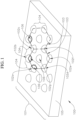
- FIG. 1 depicts an example embodiment of a structure 100.
- Structure 100 may comprise nanostructures 101.
- Nanostructures 101 may be embedded within a substrate 105, or may be on top of a substrate 105. Nanostructures 101 may be organized in a pattern 103.
- nanostructures 101 may be gold, aluminum, silver, copper, aluminum-doped zinc oxide, Indium tin oxide, titanium nitride, indium gallium arsenide, tungsten oxide, titanium-tungsten or any other metals or metal alloys, however, they may be made of other materials as well, not listed. Nanostructures 101 may be distributed or located in a pattern 103 on or within substrate 105. Pattern 103 may be periodic, which may be a repeatable distribution of nanostructures. Pattern 103 may have equidistant nanostructures 101, such as a hexagonal pattern. Pattern 103 may have both equidistant and non-equidistant structures (i.e.
- Pattern 103 may be periodic or it may be semi-periodic, where there may be a repeatable pattern for some of the nanostructures while there is a non-repeatable pattern for other parts of the nanostructure.
- pattern 103 may form a tessellation, which may be a tile.
- the tessellation may be overlapping or may be non-overlapping.
- Pattern 103 may be a periodic pattern that may provide an equidistant spacing of nanostructures 101. Equidistant may be an approximation where the distances between nanostructures are approximately equal but may have variations due to the accuracy limitations of fabrication techniques, which will be described later in more detail.
- pattern 103 may be six-sided, which may be a hexagonal tile pattern, which may also be known as a hexagonal lattice. Nanostructures 101 may form a hexagonal tile pattern, where six nanostructures can form the six vertices of a hexagon. In some embodiments, nanostructures 102a-f may form pattern 103 for the example case of a hexagonal pattern. There may be an additional nanostructure embedded within pattern 103, such as at the center of pattern 103 which may be nanostructure 102g. Nanostructure 102g may form a vertex of another pattern 103 of nanostructures.
- Nanostructure 102a may be a first distance 104 away from nanostructure 102b.
- First distance 104 may be known as a lattice constant, and may be the distance between the center of nanostructure 102a and the center of nanostructure 102b.
- nanostructure 102b may be a first distance 104 away from nanostructure 102c.
- First distance 104 may be based on a target wavelength of structure 100 and the structure 100 may be designed for peak wavelength reflection, which will be described in more detail in FIG. 2 .
- first distance 104 may be between 60 nm and 600 nm. In other embodiments, first distance 104 may be greater for longer target wavelengths and may be less for shorter target wavelengths.
- the angle between the edge formed by nanostructure 102a to nanostructure 102b and nanostructure 102b to nanostructure 102c may be a first angle 106.
- first angle 106 may be about 120 degrees.
- the first distance 104 and first angle 106 may be approximately the same for all edges and angles of pattern 103 for all subsequent nanostructures 102a-f.
- pattern 103 may be any shape that can be tessellated.
- pattern 103 may maintain the equidistant and equal-angle properties for all nanostructures as described previously.
- pattern 103 may not be have fully equidistance and equal-angled nanostructures.
- pattern 103 may not be periodic, that is, there may be a fixed pattern where nanostructures 101 may not be equidistant from each other.
- pattern 103 may alternatively be expressed as a tiling of the triangles (e.g., equilateral triangles or isosceles triangles) that make up a hexagonal or square pattern.
- substrate 105 may be a flexible or stretchable material that may allow for flexing of the substrate, such as polydimethylsiloxane (PDMS), but may be other materials as well.
- substrate 105 may be rigid, such as nickel, but may be other materials as well.
- substrate 105 may be between 100 nm to 50 ⁇ m thick.
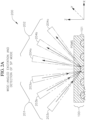
- FIG. 2A depicts a side view 200 of structure 100 of FIG. 1 .
- a spectrum 201 may travel onto structure 100 at a first angle of incidence 203a, which may also be known as a first angle 203a.
- First angle 203a may be any angle between 0 degrees (parallel to the plane of structure 100) and 90 degrees (perpendicular to the plane of structure 100).
- spectrum 201 may comprise any wavelength or range of wavelengths, which may be known as broadband light, in the visible and near-infrared spectrum.
- spectrum 201 may be in a different spectrum range, such as near-infrared, ultraviolet, microwave, or other wavelength range.
- Spectrum 201 may interact with structure 100 and produce a reflected spectrum 202, which may be reflected from structure 100 at a first angle of reflection 204a.
- First angle of reflection 204a may be any angle between 90 degrees (perpendicular to the plane of structure 100) and 180 degrees (parallel to the plane of structure 100).
- Reflected spectrum 202 may have a peak wavelength, which may also be known as the target wavelength, that is reflected and all other wavelengths may have little to no reflection, which will be described in more detail below.
- the first angle of reflection 204a may depend on the first angle of incidence 203a.
- the second angle of reflection 204b may depend on the second angle of incidence 203b, and so on.
- reflected spectrum 202 may be approximately the same for all angles of angles of incidence 203a-c. That is, the response of structure 100 to spectrum 201 may be angle-independent. Angle-independence may not be truly independent, that is, there may be some variations in the exact peak wavelength reflected in reflected spectrum 202 based on the angles of incidence 203a-c, but such angle dependence is greatly reduced compared to other metamaterials.
- the peak wavelength reflected may vary slightly based on the angle of incidence 203a-c.
- spectrum 201 may be broadband light spanning 500nm - 1000nm.
- First angle of incidence 203a may be 30 degrees
- second angle 203b may be 45 degrees
- third angle 203c may be 60 degrees.
- reflected spectrum 202 may have a first peak wavelength of about 600 nm for first angle 203a, a second peak wavelength of about 602 nm for second angle 203b, and a third peak wavelength of about 604 nm for a third angle 203c.
- the first, second, and third peak wavelengths may be substantially similar so as to apply the term "angle-independent," however, there may still be small wavelength variations in reflected spectrum 202 based on the angles of incidence 203a-c.
- the peak wavelength for any given angle may change when structure 100 is stretched or compressed. If structure 100 is stretched or compressed, reflected spectrum 202 may have a new peak wavelength that is different than the first peak wavelength. The difference between the new peak wavelength and the first peak wavelength may be used to infer a change in pressure, as described further below.
- the peak wavelength may change when structure 100 is exposed to and/or in contact with a liquid or other material.
- the composition of the liquid or other material may be determined based on the change in peak wavelength. If structure 100 exposes nanostructures 101 and a liquid or new material is in contact with nanostructures 101, such as a fluid, reflected spectrum 202 may have a different peak wavelength relative to the peak wavelength in absence of the material. The difference between the first and different peak wavelengths may be used to infer information such as the presence of a certain material in contact with structure 100, and may be discussed in more detail later in the description.
- Structure 100 may also be polarization-independent. That is, the reflected spectrum 202 may be polarization independent.
- spectrum 201 may have different transverse electric (TE) or transverse magnetic (TM) polarizations. That is, for any polarization of spectrum 201, reflected spectrum 202 may be approximately the same.
- TE transverse electric
- TM transverse magnetic
- FIG. 2B depicts a side view 210 of nanostructure 102a.
- the z-axis may depict the height of nanostructure 102a and the x-axis may depict the width of nanostructure 102a.
- nanostructure 102a may be at its widest point, which may be its diameter.
- the diameter of the nanostructure 102a is defined as the intersection of the nanostructure 102a and the base substrate on which the nanostructure 102a is formed.
- the cross section of nanostructure 102a may be shown along the Z-X plane.
- the diameter of nanostructure 102a at its base may be 200nm, but may be other diameters between 10nm and 2000nm.
- the height of nanostructure 102a may be 100nm, but may be other heights, for example, between 36nm and 168nm.
- nanostructure 102a may change based on the target wavelength and the material used. Resolving the height and the diameter of the nanostructures for a target wavelength requires solving for two variables (height and diameter), and as one varies within an acceptable range, the other will vary accordingly.
- the height of nanostructure 102a may be between 12% and 56% of the first distance 104.
- the diameter of nanostructure 102a may be between 40% and 80% of the first distance 104.
- the height and diameter of nanostructure 102a may be determined by checking for normal-to-plane mode for a fixed lattice constant and varying the diameter and height of nanostructure 102a.
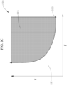
- an experimental test 220 based on experimentally varied height and diameter values, and which may compare the variables f and r for a fixed lattice constant value.
- a lattice constant value may be determined based on a target wavelength, and the final height and diameter of nanostructure 102a may be determined based on the results of test 220.
- Test 220 may reveal regions 221 and 223 and there may be a border line 222.
- Region 223, which may include border line 222, may be a region in which normal-to-plane mode exists and may allow for the angle independent behavior.
- Region 221 may be a region in which normal-to-plane mode does not exist.
- the angle of incidence of spectrum 201 may result in a large change in peak wavelength shift of reflected spectrum 202, which will be described in more detail later in FIG. 3 and FIG. 7 .
- the angle of incidence of spectrum 201 may result in a small change in peak wavelength shift of reflected spectrum 202, relative to region 221. That is, region 223, including border line 222, may result in an angle independent or less angle dependent peak wavelength shift of reflected spectrum 202.
- the physical parameters of height, diameter, and lattice constant of nanostructure 102a may impact the peak wavelength shift of the reflected spectrum 202. However, as long as the parameters enable a normal-to-plane mode, there may be little to no differences in the measured peak wavelength shift due to angle the angle of incidence (unlike values found in region 221). Therefore, it may be advantageous to select a height and diameter value that may be on border line 222.
- the lattice constant, first distance 104 may be determined based on a target wavelength, which may be the peak wavelength reflected for reflected spectrum 202 and may be approximately 1 ⁇ 2 the target wavelength. For example, if a target wavelength is 620 nm, the lattice constant may be about 300 nm. For a range of diameter, height, and lattice constant values, a normal-to-plane mode may exist to allow reflected spectrum 202 to have a peak wavelength shift. In some ranges of f and r, the peak wavelength shift for reflected spectrum 202 may be greater than for other ranges of f and r.
- nanostructure 102a may comprise gold, f may be in the range of 0.4 to 0.8, and r may be in the range of 0.3 to 0.7. Therefore, f*r may be in range of 0.3*0.4, 0.12 to 0.8*0.7, 0.56, providing the ratio to be 12% to 56% of height of nanostructure 102a to first distance 104. In other embodiments, other ratios may exist. This embodiment may be for the visible spectrum for spectrum 201. In another embodiment, spectrum 201 may be near infrared (NIR), and other metals may be used, which may include gold, silver, or aluminum.
- NIR near infrared
- nanostructure 102a may have a cross section in the Z-X plane that may be based on a paraboloid in shape, however, other shapes may be used, including square, rectangular, spherical, trapezoidal, hemi-ellipsoid, or other shape.
- a paraboloid may be a quadric surface with one axis of symmetry (Z axis for FIG. 2B ), however, nanostructure 102a may not be exactly paraboloid in shape. It may have natural variations due to physical constraints of fabrication techniques, or it may be purposefully not fully paraboloid by design.
- Nanostructure 102a may have a surface 205.
- Surface 205 may have a charge distribution 206.
- Surface 205 may have a surface plasmon (SP) mode, where the charge distribution 206 on the surface may oscillate between a positive and negative charge periodically, which may be known as periodicity.
- SP surface plasmon
- This may be known as a normal-to-plane mode which may be a resonant oscillation of conduction electrons that may occur along surface 205 of nanostructure 102a and may be according to a refractive index (RI) perceived by a wave at surface 205.
- RI refractive index
- Ez there may be an electric field polarized along the z-axis, as shown in FIG. 2B , which may be denoted as Ez.
- Ex there may be an electric field polarized along the x-axis, which may be denoted as Ex.
- Ez may be oriented perpendicular and Ex may be oriented parallel to the plane of periodicity of pattern 103 on structure 100. That is, Ez may be along the z-axis and Ex may be along the x-axis.
- the dipole moment may be substantially less dependent on the first angle of incidence 203a of spectrum 201 due to the surface plasmon mode.
- a normal-to-plane mode may be along the z-axis, which may be a SP mode where the dipole moment of nanostructure 102a may be oriented normal to the plane of periodicity irrespective of the angle and polarization of spectrum 201. As described previously, this may result in angle-independence and polarization-independence, however, there may be some variations in response based on angle and polarization. The variations may be much less than for other (Non-paraboloid) nanostructure 102a shapes and patterns 103, which will be described further in FIG. 3 .
- Nanostructure 102a may have an effective plasmonic refractive index (RI) that varies based on the depth (z-axis) between the top and the bottom of nanostructure 102a. From the top of a nanostructure 102a and to the bottom of nanostructure 102a along the z-axis, there may be a gradual increase in the effective plasmonic RI. The effective plasmonic RI may be affected by neighboring nanostructures 102a-f of FIG. 1 . As the first distance 104 increases between two nanostructures, the refractive index may decrease. As the first distance 104 decreases between two nanostructures, the refractive index may increase.
- RI effective plasmonic refractive index
- an effective plasmonic RI gradient 207 may show a relationship between the depths from the top of nanostructure 102a to the base of nanostructure 102a.
- the effective plasmonic RI, n eff may be lower at the top of nanostructure 102a and may increase linearly along the surface 205 of nanostructure 102a.
- FIG. 3 depicts an example comparison of two differently-shaped nanostructures 101 of FIG. 1 .
- There may be an array of paraboloid-shaped nanostructures 101 and an array of disk-shaped nanostructures 101, which will be described in more detail below.
- the shape of nanostructures 101 may impact the change in wavelength dependence over a range of angles of incidence for input angles 203a to 203c.
- a paraboloid array may comprise paraboloid-shaped nanostructures 101 of FIG. 1 and may exhibit a normal-to-plane mode.
- a disk array may comprise disk-shaped nanostructures 101 of FIG. 1 and may exhibit an out-of-plane mode.
- Spectrum 201 of FIG. 2 may have an input angle range 203a-c, which may be shown as between 25 degrees to 60 degrees on the X- axis in the presently illustrated example.
- Spectrum 201 may interact with nanostructures 101 on structure 100, and may result in a reflected spectrum 202 with a peak wavelength for each output angle 204a-c.
- the difference between the peak wavelength of reflected spectrum 202 at 25 degree and angles higher than 25 degree spectrum 201 may be measured and denoted as ⁇ ⁇ on the Y-axis of FIG. 3 , with units that may be in nanometers.
- a first nanostructure type 301 which may be a non-paraboloid shape, has a difference between peak reflected spectrum 202 at 25 degree and angles higher than 25 degrees, and peak spectrum 201 may change linearly with input angle range 203a-c.
- peak spectrum 201 may change linearly with input angle range 203a-c.
- ⁇ ⁇ For each five degree change in an input angle, there may be a 10% or greater change in ⁇ ⁇ . That is, there may be a change in ⁇ ⁇ that may be known as an angle-dependent response.
- an input angle 203a may be 25 degrees and ⁇ ⁇ may be about 0 nm.
- An input angle 203b may be 40 degrees and ⁇ ⁇ may be about 14 nm.
- Input angle 203c may be 60 degrees and ⁇ ⁇ may be about 30 nm.
- second nanostructure type 302 may have a paraboloid shape and there may be a much more angle-independent response than for a disk shape structure in first nanostructure type 101. There may still be an angle-dependent response for second nanostructure type 302, however, relative to first nanostructure type 301, the response may be far less and the term angle-independence may be used.
- an input angle 203a may be 25 degrees and ⁇ ⁇ may be about 0 nm.
- An input angle 203b may be 40 degrees and ⁇ ⁇ may be about 1.4 nm.
- An input angle 203c may be 60 degrees and ⁇ ⁇ may be 1.8 nm.
- FIG. 4 depicts a fabrication process 400 for fabrication of structure 100.
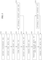
- Fig. 5 depicts a process 500 of fabrication process 400 of FIG. 4 .
- Fabrication of structure 100 may begin on a substrate 401.
- Substrate 401 may be any material upon which fabrication of structure 100 may take place. In some embodiments, substrate 401 may be made from silicon. Substrate 401 may be a silicon wafer.
- a photoresist 402 may be deposited onto substrate 401. This may be process 501 of FIG. 5 : depositing photoresist 402 onto a substrate 401.
- photoresist 402 may be about 1 micrometer ( ⁇ m ) thick. In another embodiment, photoresist 402 may be between 0.1 ⁇ m and 5 ⁇ m thick. In some embodiments, photoresist 402 may be level and approximately equal in thickness across substrate 401.
- Photoresist 402 may comprise a light-sensitive polymer material that may be used in a process to form a patterned coating on a surface, where patterning may also include removing all non-patterned photoresist 402 from a surface.
- Photoresist 402 may have an associated sensitizer and solvent. In some embodiments, photoresist 402 may be used in a positive or a negative photoresist process. The chemical structures of photoresist 402 may be photopolymeric, photodecomposing, photocrosslinking, or any other photoresist structure. In another embodiment, the photoresist 402 may be exposed by electron beams.
- photoresist 402 may be spin coated onto substrate 401 to form a uniformly thick layer. In some embodiments, photoresist 402 may then be heated to between 100 C and 120 C for 100 seconds to 200 seconds.
- Process 502 of FIG. 5 may comprise depositing a first metal 403 onto photoresist 402.
- First metal 403 may also be referred to as a substrate metal.
- some of first metal 403 may also be deposited on substrate 401 in addition to photoresist 402. This may include a region between an edge of substrate 401 and an edge of photoresist 402.
- all of first metal 403 may be deposited on photoresist 402.
- first metal layer 403 may be nickel. In another embodiment, first metal 403 may be any other metal in the periodic table, or a mixture or alloy of metals. In some embodiments, first metal layer 403 may be between 200 nm and 600 nm thick and may be used as a sacrificial layer. In some embodiments, first metal layer 403 may be deposited using electron beam (e-beam) evaporation. In some embodiments, the speed of evaporation of first metal 403 may be 0.05 nm/s to 5 nm/s.
- e-beam electron beam
- Process 503 of FIG. 5 may comprise depositing resist 404 onto first metal layer 403.
- resist 404 may be a synthetic resin, such as polymethyl methacrylate (PMMA).
- resist 404 may be a ZEON electron beam positive-tone (ZEP) resist, as marketed and sold by ZEON SPECIALTY MATERIALS, INC.
- ZEP ZEON electron beam positive-tone
- resist 404 may be any kind of electron-beam resist.
- resist 404 may be spin coated onto first metal 403. In some embodiments, the time to bake resist 404 may be between 100 seconds and 200 seconds. In some embodiments, resist 404 may be baked at between 150 C and 200 C.
- resist 404 may be between 0.1 ⁇ m and 5 ⁇ m in thickness, however, the thickness of resist 404 may be larger or smaller and may depend on the target aspect ratio of holes 405. The thickness of resist 404 may depend on fabrication requirements, such as an aspect ratio of patterns formed on resist 404.
- electron beam (e-beam) lithography may be applied to resist 404 to form a pattern of holes, for forming the pattern 103 of FIG. 1 .
- Process 504 of FIG. 5 may comprise forming pattern 103 on resist 404.
- the beam of the e-beam lithography may be between a 5 to 100 nano-Amp beam with a power intensity of 1000 - 5000 micro-coloumbs per cubic centimeter, and may be other values beyond this range.
- the e-beam lithography applied to resist 404 may form holes 405 with a pattern 103. Holes 405 may expose first metal 403 at the location of holes 405. Pattern 103 of holes 405 may be used to aid in the formation of nanostructures 101.
- a hole of the holes 405 may have an aspect ratio, which may be the ratio of the height of the hole to the diameter of the hole. In some embodiments, the aspect ratio may be between 3 and 16.
- the diameter of a hole of the holes 405 may be between 100 nm and 1 um, however, the diameter of the hole may be greater or smaller depending on the target wavelength application. In some embodiments, the diameter of a hole in holes 405 may be within an order of magnitude of the target wavelength application. In another embodiment, there may be multiple diameters of holes used in holes 405.
- a layer 406 may be deposited onto first metal 403 at the location of holes 405.
- Process 505 of FIG. 5 may comprise optionally depositing layer 406 onto first metal 403.
- Layer 406 may be an adhesion layer and may be used to aid in the deposition process of metals.
- Layer 406 may be a metal, such as chromium, and may be between 1nm and 5nm in thickness. Layer 406 may also be known as an adhesion layer. Layer 406 may allow for better adhesion between first metal 403 and a second metal 407.
- a second metal 407 may be deposited onto part of or all of layer 406 at the location of holes 405, which may be the same location as pattern 103 and may form pattern 103. Second metal 407 may also be referred to as a nanostructure metal. In another embodiment, where first metal 403 is not used, second metal 407 may be deposited onto any substrate at the location of holes 405. Process 506 of FIG. 5 comprises depositing second metal 407 at the location of holes 405. In another embodiment, second metal 407 may be deposited onto first metal 403 at the location of holes 405 when layer 406 is not present.
- second metal 407 may be gold, however, it may be other metals, including aluminum, silver, copper, aluminum-doped zinc oxide, Indium tin oxide, titanium nitride, indium gallium arsenide, tungsten oxide, titanium-tungsten or any other metals or metal alloys. In some embodiments, second metal 407 is between 50 nm and 500 nm thick, but may be other thicknesses depending on the target wavelength application, as described previously.
- a target wavelength application may be the wavelength at which nanostructures 101 interact with the target wavelength and may be the peak wavelength reflected in reflected spectrum 202 of FIG. 2A . In some embodiments, the second metal 407 chosen may depend on the target wavelength.
- second metal 407 may be gold, but it may be other metals.
- second metal 407 may be aluminum or silver, but it may be other metals.
- the spectrum range a metal reflects at may be used to determine the metal to select for the target wavelength. Gold may be able to reflect visible spectrum, whereas aluminum and silver may be able to reflect NIR spectrum.
- second metal 407 may be deposited using e-beam deposition, however, other deposition methods may be used.
- Second metal 407 once deposited, may be initially in a shape 408.
- shape 408 may be a cone shape.
- the top of the cone may be flat or level, and may not finish at a singular point.
- the cone shape may be formed as a result of the aspect ratio of holes 405. If the aspect ratio is low, shape 408 may look more like a disk. If the aspect ratio is high, shape 408 may look more like a cone with a sharp, singular point as its tip.
- the shaping of second metal 407 from shape 408 into a shape 409 may occur after resist 404 is removed.
- resist 404 may be removed.
- Process 507 of FIG. 5 comprises removing resist 404.
- Resist 404 may be removed with a lift-off bath method using a solvent stripper such as REMOVER PG, as marketed and sold by KAYUKA ADVANCED MATERIALS.
- REMOVER PG may be used and resist 404 may be in a lift-off bath for 6 to 30 hours.
- a different method may be used to remove resist 404.
- Second metal 407 may be in shape 408 and may be transformed to shape 409 without resist 404.
- Process 508 of FIG. 5 may comprise transforming second metal 407 from shape 408 to shape 409.
- shape 409 may be paraboloid in shape.
- shape 409 may be a disk, cone, or hemi-sphere.
- exposure to an ion beam may be used to shape second metal 407 from shape 408 to shape 409.
- Focused-ion beam exposure may be used to form second metal 407 into shape 409, with a 0.1 to 2 nano-Amp beam which may have a 0.01 to 1 millisecond dwell time. Dwell time may be the exposure time of the ion beam to second metal 407.
- the focused-ion beam may be a directional beam, which may allow the edges of the second metal 407 in shape 408 to wear off. That is, the focused-ion beam may be directional, which may be perpendicular to the substrate 401 in some embodiments.
- the sharp features facing the focused-ion beam directions, such as edges, points, or flat surfaces, may be removed.
- the direction of the ion beam may be at an angle between 0 degrees (parallel) and 90 degrees (perpendicular) to substrate 401. In some embodiments, the direction may not change during the dwell time where the ion beam is being exposed. In another embodiment, the direction may change during the dwell time where the ion beam is being exposed.
- Process 509 of FIG.5 may comprise optionally depositing surface 410 onto second metal 407.
- surface 410 may be PDMS and may be deposited via spin coating, however, surface 410 may be other materials, such as materials that are elastic or that may allow waves to travel through it and may be deposited by another technique. In some embodiments, surface 410 may be between 1 and 100 times the height of second metal 407. Surface 410 may be an optional surface and may not be deposited onto second metal 407 in some embodiments.
- first metal 403 may extend beyond the base of photoresist 402. This extended area may be cut away and the structure of photoresist 402, first metal 403, layer 406 (if included in the deposition process), second metal 407, and surface 410 may be removed from substrate 401. Photoresist 402 may then be removed by using a solvent, such as acetone. In some embodiments, acetone solvent may be used for between 2 and 10 minutes to remove photoresist 402.
- first metal 403 may be removed with an acid bath.
- Process 510 of FIG.5 may comprise removing first metal 403.
- Hydrochloric acid may be used and the structure may be in an acid bath for between 12 and 36 hours.
- first metal 403 may be removed with alternate methods.
- the resulting structure may be structure 100 which may comprise layer 406, second metal 407, and surface 410.
- layer 406 may also be removed using the hydrochloric acid bath.
- first metal 403 and layer 402 may not be needed and the resulting structure may be directly fabricated on substrate 401. Subsequently, process 502 and process 503 may not occur.
- This embodiment may be for a structure 100 where nanostructures 101 are exposed and are on the surface of substrate 401 with no surface 410 present.
- process 510 may not occur and no acid bath may be used. Instead, substrate 401 may be cut to form structure 100.
- the resulting structure may be structure 100 which may comprise second metal 407, and surface 410.
- structure 100 may comprise second metal 407 and surface 410 when layer 406 is not used.
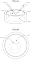
- FIG. 6A depicts a perspective view of an example embodiment of a sensor 600 and FIG. 6B depicts a top view of the same.
- Sensor 600 may use structure 100 to measure a change in pressure.
- Sensor 600 may comprise a cavity 601.
- a membrane 602 may be on the top side of cavity 601.
- Structure 100 may be on membrane 602.
- Cavity 601 may be an elastomeric material, such as PDMS. Cavity 601 may be filled with a compressible fluid at a known pressure, such as air, and sealed so that if immersed in a fluid, no fluid may penetrate cavity 601. In some embodiments, cavity 601 may be a cylinder with a height of between 10 ⁇ m to 1 mm and diameter of between 100 ⁇ m and 5mm. Structure 100 may be attached to cavity 601 on the surface of membrane 602, or it may be embedded in membrane 602.
- membrane 602 may deflect based on a pressure differential of the outside relative to the inside.
- a spectrum 201 may be transmitted to structure 100, which may be reflected as a reflected spectrum 202, which may have an associated peak wavelength that is reflected.
- the peak wavelength reflected in reflected spectrum 202 at an unknown pressure may be compared to the peak wavelength observed when the pressure differential is known to determine a pressure change in membrane 602.
- Cavity 601 may experience a pressure differential between its internal cavity 601 fluid and the external environment, which may deflect membrane 602.
- the deflection of membrane 602 may result in radial strain on structure 100, which may cause the nanostructures 101 embedded within structure 100 to become more or less tightly spaced. This in turn causes a change in peak wavelength, which may be used to estimate the pressure differential, as will be described in FIG. 7 .
- cavity 601 may be placed in the anterior chamber of an eye, in a position that may be outside of the field of view. An eye pressure change may lead to a pressure change in cavity 601, which may in turn cause membrane 602 to deflect and structure 100 to deflect.
- structure 100 may also be used without cavity 601.
- membrane 602 and structure 100 may form a sensor without cavity 601.
- Structure 100 may be embedded in membrane 602, or may be placed on top of membrane 602. With structure 100 embedded in membrane 602, the resulting configuration may be used as a sensor for measuring the stretch or compression of the material when placed on a surface. With structure 100 placed on top of membrane 602, the resulting structure may be used to detect the composition of a material or liquid placed on top of or in direct contact with structure 100.
- FIG. 7 depicts a pressure measurement 700 of sensor 600 of FIG. 6 with structure 100.
- FIG. 7 may compare the change in peak wavelength of reflected spectrum 202 at varying pressures for structures 100 with a first nanostructure type 301 and a second nanostructure type 302 of FIG. 3 .
- FIG.7 may illustrate an advantage of using paraboloid shaped nanostructures.
- the x-axis may show a change in wavelength
- the y-axis may show a reflectivity of reflected spectrum 202 in arbitrary units (a.u.). Reflection may be measured in photon counts that may be measured by a spectrometer. They photon count may vary depending on the physical environment, light source power, and other variables. Therefore, a.u. may be used for analyzing the reflectivity and to compare a peak wavelength shift.
- a change in peak wavelength of reflected spectrum 202 for a first nanostructure type 301 at varying pressure levels and varying angles of incidence 203a-c of FIG. 2A may be depicted in responses 701.
- a change in peak wavelength of reflected spectrum 202 for a second nanostructure type 302 at varying pressure levels and varying angles of incidence 203a-c of FIG. 2A may be depicted in responses 702.
- first nanostructure type 301 may comprise disk or other non-paraboloid shapes.
- Second nanostructure type 302 may comprise paraboloid-shaped nanostructures.
- FIG. 7 may show three angles of incidences for spectrum 201 of FIG. 2 in scenarios 710, 720, and 730.
- the angle of incidence may be 60 degrees.
- the angle of incidence may be 45 degrees, and in scenario 730, the angle of incidence may be 30 degrees.
- Scenarios 710, 720, and 730 may correspond to input angles 203a-c of FIG. 2 , respectively.
- the topmost graph line may correspond to 0 mmHg pressure change
- the middle graph line may represent a 20 mmHg pressure change
- the lowest graph line may represent 40 mmHg pressure change.
- measurement 702a may show a peak wavelength shift for second nanostructure type 302 when sensor 600 is calibrated to 0 mmHg pressure change.
- response 702 and 701 for an angle of incidence of 60 degrees.
- response 702 which may correspond to second nanostructure type 302
- Measurement 701a may correspond to a pressure change of 0 mmHg.
- Measurement 702b may correspond to a pressure change of 20 mmHg, and measurement 702c may correspond to a pressure change of 40 mmHg.
- measurement 701a may have a pressure change of 0 mmHg
- measurement 701b may have a pressure change of 20 mmHg
- measurement 701c may have a pressure change of 40 mmHg.
- Peak wavelength shift 702a may be approximately 3nm
- peak wavelength shift 703 may be approximately 2.75 nm
- peak wavelength shift 704 may be approximately 2.5 nm.
- Peak wavelength shift 701a may be approximately 25 nm
- peak wavelength shift 705 may be approximately 18 nm
- peak wavelength shift 706 may be approximately 15 nm.
- response 702 may have an angle-independent response (EG, very little peak wavelength shift) to a change in peak wavelength of spectrum 202. As described previously, angle independent may be less angle-dependent than other solutions.
- Response 702 which may use paraboloid-shaped nanostructures of second nanostructure shape 302, may have a peak wavelength shift at 0 mmHg of between 2.5 nm and 3 mm for angle of incidence ranges from 30 degrees of scenario 730 to 60 degrees of scenario 710 respectively.
- the difference in peak wavelength shift between a 30 degree and 60 degree angle of incidence may be approximately 0.5 nm.
- a difference in peak wavelength shift of 0.5 nm may not result in a color change. Therefore, if a paraboloid-shaped nanostructure is used in sensor 600, there may be an "angle independent" range where measurements may provide approximately the same readings across a range of angles of incidence.
- response 701 which may use first nanostructure type 301, which use disc-shaped nanostructures, may show an angle-dependent response to peak wavelength shifts 701a, 704, and 706.
- Response 701 may have a peak wavelength shift at 0 mmHg of between 15 nm and 25 nm for angle of incidence ranges from 30 degrees of scenario 730 to 60 degrees of scenario 710.
- the difference in peak wavelength shift between a 30 degree and 60 degree angle of incidence may be approximately 10 nm.
- a difference in peak wavelength shift of 10 nm may result in a color change. Therefore, if a disc-shaped nanostructure is used in sensor 600, there may be an "angle dependent" range where measurements may provide different readings across a range of angles of incidence.
- paraboloid-shaped nanostructures may allow for a useful sensor 600 because it may be angle independent or less dependent on angles of incidence.
- the angle of incidence of spectrum 201 may not need to be exact and it may be a range of angles, such as from 30 degrees to 60 degrees. This may be shown in responses 702. Unlike responses 702, in responses 701, there may be an angle dependent response which may not be useful for a sensor 600 because measurements may require an exact angle of incidence to provide repeatable measurements.
- Pressure measurement readings may be calibrated for sensor 600 by using the data of pressure measurement 700, specifically responses 702.
- Sensor 600 may use paraboloid-shaped nanostructures and may be calibrated to pressure measurements as shown in responses 702. That is, for a given pressure change, there may be one peak wavelength shift regardless of the angle of incidence of spectrum 201. As shown in the shaded region of responses 702, the peak wavelength shift for each pressure change is different across pressure and about the same across angles of incidence. Therefore, a problem that was previously intractable, measuring pressure across a range of angles of incidence, may now be solvable and used in sensor 600.
Landscapes
- Physics & Mathematics (AREA)
- Chemical & Material Sciences (AREA)
- General Physics & Mathematics (AREA)
- Engineering & Computer Science (AREA)
- Organic Chemistry (AREA)
- Optics & Photonics (AREA)
- Health & Medical Sciences (AREA)
- Life Sciences & Earth Sciences (AREA)
- Nanotechnology (AREA)
- Inorganic Chemistry (AREA)
- General Health & Medical Sciences (AREA)
- Medical Informatics (AREA)
- Veterinary Medicine (AREA)
- Biophysics (AREA)
- Ophthalmology & Optometry (AREA)
- Biomedical Technology (AREA)
- Heart & Thoracic Surgery (AREA)
- Materials Engineering (AREA)
- Molecular Biology (AREA)
- Surgery (AREA)
- Animal Behavior & Ethology (AREA)
- Public Health (AREA)
- Condensed Matter Physics & Semiconductors (AREA)
- Crystallography & Structural Chemistry (AREA)
- Mechanical Engineering (AREA)
- Chemical Kinetics & Catalysis (AREA)
- Metallurgy (AREA)
- Composite Materials (AREA)
- Manufacturing & Machinery (AREA)
- Investigating Or Analysing Materials By Optical Means (AREA)
- General Chemical & Material Sciences (AREA)
Claims (11)
- Metamaterialstruktur (100), die folgendes aufweist:ein Substrat (105), undNanostrukturen (101), die in einem Muster (103) auf dem Substrat angeordnet sind,
wobei die Nanostrukturen (101) parabelförmig sind und in einem periodischen Muster angeordnet sind,dadurch gekennzeichnet, dass der Abstand (104) zwischen den nächstgelegenen Nanostrukturen (101) zwischen 120 nm und 1200 nm beträgt,wobei die Nanostrukturen (101) in der Lage sind, im Normal-Ebene-Modus zu arbeiten, wobei der Normal-Ebene-Modus ferner einen winkelunabhängigen Oberflächenplasmonenmodus und einen polarisationsunabhängigen Oberflächenplasmonenmodus aufweist, undwobei die Nanostrukturen (101) eines oder mehrere der folgenden aufweisen: Gold, Aluminium, Silber, Kupfer, aluminiumdotiertes Zinkoxid, Indiumzinnoxid, Titannitrid, Indiumgalliumarsenid, Wolframoxid oder Titan-Wolfram oder eine Kombination davon. - Metamaterialstruktur nach Anspruch 1, wobei das Substrat (105) flexibel oder dehnbar ist.
- Metamaterialstruktur nach Anspruch 1 oder 2, wobei die Nanostrukturen (101) die Form eines Halbellipsoids haben.
- Metamaterialstruktur nach einem der Ansprüche 1 bis 3, wobei die Nanostrukturen (101) in einem halbperiodischen Muster angeordnet sind, das sowohl äquidistante Nanostrukturen (101) als auch nicht-äquidistante Nanostrukturen (101) aufweist.
- Metamaterialstruktur nach einem der Ansprüche 1 bis 4, wobei der Durchmesser der Nanostrukturen (101) zwischen 10 nm und 2000 nm ist.
- Metamaterialstruktur nach einem der Ansprüche 1 bis 5, wobei die Höhe der Nanostrukturen (101) zwischen 36 nm und 168 nm ist.
- Metamaterialstruktur nach einem der Ansprüche 1 bis 6, wobei das periodische Muster (103) hexagonal ist.
- Metamaterialstruktur nach einem der Ansprüche 1 bis 6, wobei das periodische Muster (103) quadratisch ist.
- Metamaterialstruktur nach einem der Ansprüche 1 bis 6, wobei das Muster (103) eine dreieckige Form aufweist.
- Metamaterialstruktur nach Anspruch 9, wobei das Muster (103) eine gleichseitige Dreiecksform aufweist.
- Metamaterialstruktur nach Anspruch 9, wobei das Muster (103) eine gleichschenklige Dreiecksform aufweist.
Applications Claiming Priority (2)
| Application Number | Priority Date | Filing Date | Title |
|---|---|---|---|
| US202163217655P | 2021-07-01 | 2021-07-01 | |
| US17/512,658 US12265200B2 (en) | 2021-07-01 | 2021-10-27 | Normal-to-plane surface plasmon mode for angle-and-polarization independent optomechanical sensing |
Publications (2)
| Publication Number | Publication Date |
|---|---|
| EP4113177A1 EP4113177A1 (de) | 2023-01-04 |
| EP4113177B1 true EP4113177B1 (de) | 2024-09-11 |
Family
ID=82399260
Family Applications (1)
| Application Number | Title | Priority Date | Filing Date |
|---|---|---|---|
| EP22174540.9A Active EP4113177B1 (de) | 2021-07-01 | 2022-05-20 | Metamaterialstruktur |
Country Status (4)
| Country | Link |
|---|---|
| US (1) | US12265200B2 (de) |
| EP (1) | EP4113177B1 (de) |
| KR (1) | KR20230005738A (de) |
| CN (1) | CN115555556A (de) |
Families Citing this family (1)
| Publication number | Priority date | Publication date | Assignee | Title |
|---|---|---|---|---|
| CN119772166B (zh) * | 2024-12-31 | 2025-08-05 | 西南科技大学 | 金属空心微纳米结构制备方法 |
Family Cites Families (14)
| Publication number | Priority date | Publication date | Assignee | Title |
|---|---|---|---|---|
| US5798027A (en) * | 1988-02-08 | 1998-08-25 | Optical Coating Laboratory, Inc. | Process for depositing optical thin films on both planar and non-planar substrates |
| US8599301B2 (en) * | 2006-04-17 | 2013-12-03 | Omnivision Technologies, Inc. | Arrayed imaging systems having improved alignment and associated methods |
| US9343490B2 (en) * | 2013-08-09 | 2016-05-17 | Zena Technologies, Inc. | Nanowire structured color filter arrays and fabrication method of the same |
| US20130065777A1 (en) | 2009-12-04 | 2013-03-14 | Trustees Of Boston University | Nanostructure biosensors and systems and methods of use thereof |
| US8462334B2 (en) | 2010-08-25 | 2013-06-11 | Weixing Lu | Sensor system with plasmonic nano-antenna array |
| KR101251379B1 (ko) * | 2011-11-17 | 2013-04-05 | 한국과학기술원 | 단결정 은 나노와이어를 이용한 광학 나노 안테나 및 그 제조 방법, 단결정 금속 나노와이어를 이용한 광학 나노 안테나 |
| US20130170018A1 (en) * | 2012-01-04 | 2013-07-04 | Triton Systems, Inc. | Switchable optical elements |
| SG10202004257WA (en) * | 2015-11-24 | 2020-06-29 | Harvard College | Atomic layer deposition process for fabricating dielectric metasurfaces for wavelengths in the visible spectrum |
| US10996172B2 (en) | 2017-04-28 | 2021-05-04 | National Institute Of Material Science | Surface-functionalized nanostructures for molecular sensing applications |
| US12055758B2 (en) * | 2019-01-28 | 2024-08-06 | B.G. Negev Technologies & Applications Ltd., At Ben-Gurion University | Structure for a waveguide facet |
| US11579523B2 (en) * | 2019-02-08 | 2023-02-14 | Ecole Polytechnique Federale De Lausanne (Epfl) | Method and system for fabricating glass-based nanostructures on large-area planar substrates, fibers, and textiles |
| US11885979B2 (en) * | 2020-01-03 | 2024-01-30 | University Of Maryland, College Park | Low-loss metasurface optics for deep UV |
| US12019208B2 (en) * | 2020-06-30 | 2024-06-25 | Third Floor Materials, Inc. | Surface with tunable emissivity based on epsilon-near-zero materials and patterned substrates |
| US12601857B2 (en) * | 2021-04-23 | 2026-04-14 | James Andrew Leskosek | Metamaterial devices for optical absorption, dispersion and directional sensing |
-
2021
- 2021-10-27 US US17/512,658 patent/US12265200B2/en active Active
-
2022
- 2022-05-17 KR KR1020220060349A patent/KR20230005738A/ko active Pending
- 2022-05-20 EP EP22174540.9A patent/EP4113177B1/de active Active
- 2022-06-28 CN CN202210746528.8A patent/CN115555556A/zh active Pending
Also Published As
| Publication number | Publication date |
|---|---|
| US12265200B2 (en) | 2025-04-01 |
| KR20230005738A (ko) | 2023-01-10 |
| EP4113177A1 (de) | 2023-01-04 |
| US20230003920A1 (en) | 2023-01-05 |
| CN115555556A (zh) | 2023-01-03 |
Similar Documents
| Publication | Publication Date | Title |
|---|---|---|
| US12117344B2 (en) | On-chip polarization detection and polarimetric imaging | |
| US7492530B2 (en) | Metallic nano-optic lenses and beam shaping devices | |
| US9182519B2 (en) | Metamaterial composition comprising frequency-selective-surface resonant element disposed on/in a dielectric flake, methods, and applications | |
| US9726788B2 (en) | Method for fabricating nanoantenna array, nanoantenna array chip and structure for lithography | |
| US20160025914A1 (en) | Dielectric Metasurface Optical Elements | |
| US20070159698A1 (en) | Antireflective member, optical element, display device, method of making stamper and method of making antireflective member using the stamper | |
| CN113640905A (zh) | 一种基于计算波前编码的偏振无关消色差超透镜 | |
| US20240168358A1 (en) | High Quality Factor Metasurfaces for Wavefront Manipulation | |
| US20220397703A1 (en) | Method of manufacture of a metasurface | |
| WO2016168093A1 (en) | Partially etched phase-transforming optical element | |
| JP2020094973A (ja) | 金属・誘電体・金属の3層構造を有する光変調構造体、その製造方法及び用途 | |
| EP3182178A1 (de) | Optisches element | |
| Glaser et al. | High temperature resistant antireflective moth-eye structures for infrared radiation sensors | |
| EP3667376B1 (de) | Flache metalinse und abdeckglas damit | |
| US12055738B2 (en) | Partially etched phase-transforming optical element | |
| EP4113177A1 (de) | Metamaterialstruktur | |
| EP4502663A1 (de) | Optische linse | |
| CN115421223B (zh) | 一种基于抛物线相位超表面的频率色散器件 | |
| US20240402008A1 (en) | Meta-material interferometry systems and methods | |
| US20240402407A1 (en) | Meta-material interferometry systems and methods | |
| US20240402010A1 (en) | Meta-material interferometry systems and methods | |
| Shimura et al. | Birefringence Modulation of Reconfigurable Metasurface Based on Thermal Bimorph Actuator at the Visible Range | |
| Cruz-Cabrera et al. | Fabrication and testing of plasmonic optimized transmission and reflection coatings | |
| Davanco et al. | Nanofabrication and Characterization of Subwavelength Metamaterials for Negative-index Propagation at Near-infrared Wavelengths | |
| Lee et al. | Blazed-binary diffractive gratings with antireflection coating for improved operation at 10.6 µm |
Legal Events
| Date | Code | Title | Description |
|---|---|---|---|
| PUAI | Public reference made under article 153(3) epc to a published international application that has entered the european phase |
Free format text: ORIGINAL CODE: 0009012 |
|
| STAA | Information on the status of an ep patent application or granted ep patent |
Free format text: STATUS: THE APPLICATION HAS BEEN PUBLISHED |
|
| AK | Designated contracting states |
Kind code of ref document: A1 Designated state(s): AL AT BE BG CH CY CZ DE DK EE ES FI FR GB GR HR HU IE IS IT LI LT LU LV MC MK MT NL NO PL PT RO RS SE SI SK SM TR |
|
| STAA | Information on the status of an ep patent application or granted ep patent |
Free format text: STATUS: REQUEST FOR EXAMINATION WAS MADE |
|
| 17P | Request for examination filed |
Effective date: 20230110 |
|
| RBV | Designated contracting states (corrected) |
Designated state(s): AL AT BE BG CH CY CZ DE DK EE ES FI FR GB GR HR HU IE IS IT LI LT LU LV MC MK MT NL NO PL PT RO RS SE SI SK SM TR |
|
| P01 | Opt-out of the competence of the unified patent court (upc) registered |
Effective date: 20230520 |
|
| GRAP | Despatch of communication of intention to grant a patent |
Free format text: ORIGINAL CODE: EPIDOSNIGR1 |
|
| STAA | Information on the status of an ep patent application or granted ep patent |
Free format text: STATUS: GRANT OF PATENT IS INTENDED |
|
| INTG | Intention to grant announced |
Effective date: 20240613 |
|
| GRAS | Grant fee paid |
Free format text: ORIGINAL CODE: EPIDOSNIGR3 |
|
| GRAA | (expected) grant |
Free format text: ORIGINAL CODE: 0009210 |
|
| STAA | Information on the status of an ep patent application or granted ep patent |
Free format text: STATUS: THE PATENT HAS BEEN GRANTED |
|
| AK | Designated contracting states |
Kind code of ref document: B1 Designated state(s): AL AT BE BG CH CY CZ DE DK EE ES FI FR GB GR HR HU IE IS IT LI LT LU LV MC MK MT NL NO PL PT RO RS SE SI SK SM TR |
|
| REG | Reference to a national code |
Ref country code: GB Ref legal event code: FG4D |
|
| REG | Reference to a national code |
Ref country code: CH Ref legal event code: EP |
|
| REG | Reference to a national code |
Ref country code: DE Ref legal event code: R096 Ref document number: 602022005982 Country of ref document: DE |
|
| REG | Reference to a national code |
Ref country code: IE Ref legal event code: FG4D |
|
| REG | Reference to a national code |
Ref country code: NL Ref legal event code: FP |
|
| REG | Reference to a national code |
Ref country code: LT Ref legal event code: MG9D |
|
| PG25 | Lapsed in a contracting state [announced via postgrant information from national office to epo] |
Ref country code: NO Free format text: LAPSE BECAUSE OF FAILURE TO SUBMIT A TRANSLATION OF THE DESCRIPTION OR TO PAY THE FEE WITHIN THE PRESCRIBED TIME-LIMIT Effective date: 20241211 |
|
| PG25 | Lapsed in a contracting state [announced via postgrant information from national office to epo] |
Ref country code: GR Free format text: LAPSE BECAUSE OF FAILURE TO SUBMIT A TRANSLATION OF THE DESCRIPTION OR TO PAY THE FEE WITHIN THE PRESCRIBED TIME-LIMIT Effective date: 20241212 Ref country code: FI Free format text: LAPSE BECAUSE OF FAILURE TO SUBMIT A TRANSLATION OF THE DESCRIPTION OR TO PAY THE FEE WITHIN THE PRESCRIBED TIME-LIMIT Effective date: 20240911 |
|
| PG25 | Lapsed in a contracting state [announced via postgrant information from national office to epo] |
Ref country code: BG Free format text: LAPSE BECAUSE OF FAILURE TO SUBMIT A TRANSLATION OF THE DESCRIPTION OR TO PAY THE FEE WITHIN THE PRESCRIBED TIME-LIMIT Effective date: 20240911 |
|
| PG25 | Lapsed in a contracting state [announced via postgrant information from national office to epo] |
Ref country code: LV Free format text: LAPSE BECAUSE OF FAILURE TO SUBMIT A TRANSLATION OF THE DESCRIPTION OR TO PAY THE FEE WITHIN THE PRESCRIBED TIME-LIMIT Effective date: 20240911 |
|
| PG25 | Lapsed in a contracting state [announced via postgrant information from national office to epo] |
Ref country code: HR Free format text: LAPSE BECAUSE OF FAILURE TO SUBMIT A TRANSLATION OF THE DESCRIPTION OR TO PAY THE FEE WITHIN THE PRESCRIBED TIME-LIMIT Effective date: 20240911 |
|
| PG25 | Lapsed in a contracting state [announced via postgrant information from national office to epo] |
Ref country code: RS Free format text: LAPSE BECAUSE OF FAILURE TO SUBMIT A TRANSLATION OF THE DESCRIPTION OR TO PAY THE FEE WITHIN THE PRESCRIBED TIME-LIMIT Effective date: 20241211 Ref country code: ES Free format text: LAPSE BECAUSE OF FAILURE TO SUBMIT A TRANSLATION OF THE DESCRIPTION OR TO PAY THE FEE WITHIN THE PRESCRIBED TIME-LIMIT Effective date: 20240911 |
|
| PG25 | Lapsed in a contracting state [announced via postgrant information from national office to epo] |
Ref country code: RS Free format text: LAPSE BECAUSE OF FAILURE TO SUBMIT A TRANSLATION OF THE DESCRIPTION OR TO PAY THE FEE WITHIN THE PRESCRIBED TIME-LIMIT Effective date: 20241211 Ref country code: NO Free format text: LAPSE BECAUSE OF FAILURE TO SUBMIT A TRANSLATION OF THE DESCRIPTION OR TO PAY THE FEE WITHIN THE PRESCRIBED TIME-LIMIT Effective date: 20241211 Ref country code: LV Free format text: LAPSE BECAUSE OF FAILURE TO SUBMIT A TRANSLATION OF THE DESCRIPTION OR TO PAY THE FEE WITHIN THE PRESCRIBED TIME-LIMIT Effective date: 20240911 Ref country code: HR Free format text: LAPSE BECAUSE OF FAILURE TO SUBMIT A TRANSLATION OF THE DESCRIPTION OR TO PAY THE FEE WITHIN THE PRESCRIBED TIME-LIMIT Effective date: 20240911 Ref country code: GR Free format text: LAPSE BECAUSE OF FAILURE TO SUBMIT A TRANSLATION OF THE DESCRIPTION OR TO PAY THE FEE WITHIN THE PRESCRIBED TIME-LIMIT Effective date: 20241212 Ref country code: FI Free format text: LAPSE BECAUSE OF FAILURE TO SUBMIT A TRANSLATION OF THE DESCRIPTION OR TO PAY THE FEE WITHIN THE PRESCRIBED TIME-LIMIT Effective date: 20240911 Ref country code: ES Free format text: LAPSE BECAUSE OF FAILURE TO SUBMIT A TRANSLATION OF THE DESCRIPTION OR TO PAY THE FEE WITHIN THE PRESCRIBED TIME-LIMIT Effective date: 20240911 Ref country code: BG Free format text: LAPSE BECAUSE OF FAILURE TO SUBMIT A TRANSLATION OF THE DESCRIPTION OR TO PAY THE FEE WITHIN THE PRESCRIBED TIME-LIMIT Effective date: 20240911 |
|
| REG | Reference to a national code |
Ref country code: AT Ref legal event code: MK05 Ref document number: 1723187 Country of ref document: AT Kind code of ref document: T Effective date: 20240911 |
|
| PG25 | Lapsed in a contracting state [announced via postgrant information from national office to epo] |
Ref country code: IS Free format text: LAPSE BECAUSE OF FAILURE TO SUBMIT A TRANSLATION OF THE DESCRIPTION OR TO PAY THE FEE WITHIN THE PRESCRIBED TIME-LIMIT Effective date: 20250111 Ref country code: PT Free format text: LAPSE BECAUSE OF FAILURE TO SUBMIT A TRANSLATION OF THE DESCRIPTION OR TO PAY THE FEE WITHIN THE PRESCRIBED TIME-LIMIT Effective date: 20250113 |
|
| PG25 | Lapsed in a contracting state [announced via postgrant information from national office to epo] |
Ref country code: RO Free format text: LAPSE BECAUSE OF FAILURE TO SUBMIT A TRANSLATION OF THE DESCRIPTION OR TO PAY THE FEE WITHIN THE PRESCRIBED TIME-LIMIT Effective date: 20240911 Ref country code: SM Free format text: LAPSE BECAUSE OF FAILURE TO SUBMIT A TRANSLATION OF THE DESCRIPTION OR TO PAY THE FEE WITHIN THE PRESCRIBED TIME-LIMIT Effective date: 20240911 |
|
| PG25 | Lapsed in a contracting state [announced via postgrant information from national office to epo] |
Ref country code: EE Free format text: LAPSE BECAUSE OF FAILURE TO SUBMIT A TRANSLATION OF THE DESCRIPTION OR TO PAY THE FEE WITHIN THE PRESCRIBED TIME-LIMIT Effective date: 20240911 Ref country code: AT Free format text: LAPSE BECAUSE OF FAILURE TO SUBMIT A TRANSLATION OF THE DESCRIPTION OR TO PAY THE FEE WITHIN THE PRESCRIBED TIME-LIMIT Effective date: 20240911 |
|
| PG25 | Lapsed in a contracting state [announced via postgrant information from national office to epo] |
Ref country code: PL Free format text: LAPSE BECAUSE OF FAILURE TO SUBMIT A TRANSLATION OF THE DESCRIPTION OR TO PAY THE FEE WITHIN THE PRESCRIBED TIME-LIMIT Effective date: 20240911 Ref country code: CZ Free format text: LAPSE BECAUSE OF FAILURE TO SUBMIT A TRANSLATION OF THE DESCRIPTION OR TO PAY THE FEE WITHIN THE PRESCRIBED TIME-LIMIT Effective date: 20240911 |
|
| PG25 | Lapsed in a contracting state [announced via postgrant information from national office to epo] |
Ref country code: SK Free format text: LAPSE BECAUSE OF FAILURE TO SUBMIT A TRANSLATION OF THE DESCRIPTION OR TO PAY THE FEE WITHIN THE PRESCRIBED TIME-LIMIT Effective date: 20240911 Ref country code: IT Free format text: LAPSE BECAUSE OF FAILURE TO SUBMIT A TRANSLATION OF THE DESCRIPTION OR TO PAY THE FEE WITHIN THE PRESCRIBED TIME-LIMIT Effective date: 20240911 |
|
| REG | Reference to a national code |
Ref country code: DE Ref legal event code: R097 Ref document number: 602022005982 Country of ref document: DE |
|
| PG25 | Lapsed in a contracting state [announced via postgrant information from national office to epo] |
Ref country code: DK Free format text: LAPSE BECAUSE OF FAILURE TO SUBMIT A TRANSLATION OF THE DESCRIPTION OR TO PAY THE FEE WITHIN THE PRESCRIBED TIME-LIMIT Effective date: 20240911 |
|
| PLBE | No opposition filed within time limit |
Free format text: ORIGINAL CODE: 0009261 |
|
| STAA | Information on the status of an ep patent application or granted ep patent |
Free format text: STATUS: NO OPPOSITION FILED WITHIN TIME LIMIT |
|
| 26N | No opposition filed |
Effective date: 20250612 |
|
| PG25 | Lapsed in a contracting state [announced via postgrant information from national office to epo] |
Ref country code: SE Free format text: LAPSE BECAUSE OF FAILURE TO SUBMIT A TRANSLATION OF THE DESCRIPTION OR TO PAY THE FEE WITHIN THE PRESCRIBED TIME-LIMIT Effective date: 20240911 |
|
| REG | Reference to a national code |
Ref country code: CH Ref legal event code: H13 Free format text: ST27 STATUS EVENT CODE: U-0-0-H10-H13 (AS PROVIDED BY THE NATIONAL OFFICE) Effective date: 20251223 |
|
| PG25 | Lapsed in a contracting state [announced via postgrant information from national office to epo] |
Ref country code: LU Free format text: LAPSE BECAUSE OF NON-PAYMENT OF DUE FEES Effective date: 20250520 |
|
| PG25 | Lapsed in a contracting state [announced via postgrant information from national office to epo] |
Ref country code: CH Free format text: LAPSE BECAUSE OF NON-PAYMENT OF DUE FEES Effective date: 20250531 |
|
| REG | Reference to a national code |
Ref country code: BE Ref legal event code: MM Effective date: 20250531 |
|
| PG25 | Lapsed in a contracting state [announced via postgrant information from national office to epo] |
Ref country code: MC Free format text: LAPSE BECAUSE OF FAILURE TO SUBMIT A TRANSLATION OF THE DESCRIPTION OR TO PAY THE FEE WITHIN THE PRESCRIBED TIME-LIMIT Effective date: 20240911 |
|
| PGFP | Annual fee paid to national office [announced via postgrant information from national office to epo] |
Ref country code: GB Payment date: 20260313 Year of fee payment: 5 |
|
| PG25 | Lapsed in a contracting state [announced via postgrant information from national office to epo] |
Ref country code: IE Free format text: LAPSE BECAUSE OF NON-PAYMENT OF DUE FEES Effective date: 20250520 |
|
| PG25 | Lapsed in a contracting state [announced via postgrant information from national office to epo] |
Ref country code: BE Free format text: LAPSE BECAUSE OF NON-PAYMENT OF DUE FEES Effective date: 20250531 |
|
| PG25 | Lapsed in a contracting state [announced via postgrant information from national office to epo] |
Ref country code: FR Free format text: LAPSE BECAUSE OF NON-PAYMENT OF DUE FEES Effective date: 20250531 |
|
| PGFP | Annual fee paid to national office [announced via postgrant information from national office to epo] |
Ref country code: NL Payment date: 20260409 Year of fee payment: 5 |
|
| PG25 | Lapsed in a contracting state [announced via postgrant information from national office to epo] |
Ref country code: LT Free format text: LAPSE BECAUSE OF FAILURE TO SUBMIT A TRANSLATION OF THE DESCRIPTION OR TO PAY THE FEE WITHIN THE PRESCRIBED TIME-LIMIT Effective date: 20240911 |
|
| PGFP | Annual fee paid to national office [announced via postgrant information from national office to epo] |
Ref country code: DE Payment date: 20260324 Year of fee payment: 5 |
|
| PG25 | Lapsed in a contracting state [announced via postgrant information from national office to epo] |
Ref country code: CY Free format text: LAPSE BECAUSE OF FAILURE TO SUBMIT A TRANSLATION OF THE DESCRIPTION OR TO PAY THE FEE WITHIN THE PRESCRIBED TIME-LIMIT Effective date: 20240911 |