EP4113159A1 - Laser emitting module, depth camera and electronic device - Google Patents
Laser emitting module, depth camera and electronic device Download PDFInfo
- Publication number
- EP4113159A1 EP4113159A1 EP21218132.5A EP21218132A EP4113159A1 EP 4113159 A1 EP4113159 A1 EP 4113159A1 EP 21218132 A EP21218132 A EP 21218132A EP 4113159 A1 EP4113159 A1 EP 4113159A1
- Authority
- EP
- European Patent Office
- Prior art keywords
- laser
- assembly
- circuit board
- lens
- beam outlet
- Prior art date
- Legal status (The legal status is an assumption and is not a legal conclusion. Google has not performed a legal analysis and makes no representation as to the accuracy of the status listed.)
- Granted
Links
Images


Classifications
-
- G—PHYSICS
- G01—MEASURING; TESTING
- G01S—RADIO DIRECTION-FINDING; RADIO NAVIGATION; DETERMINING DISTANCE OR VELOCITY BY USE OF RADIO WAVES; LOCATING OR PRESENCE-DETECTING BY USE OF THE REFLECTION OR RERADIATION OF RADIO WAVES; ANALOGOUS ARRANGEMENTS USING OTHER WAVES
- G01S7/00—Details of systems according to groups G01S13/00, G01S15/00, G01S17/00
- G01S7/48—Details of systems according to groups G01S13/00, G01S15/00, G01S17/00 of systems according to group G01S17/00
- G01S7/481—Constructional features, e.g. arrangements of optical elements
- G01S7/4814—Constructional features, e.g. arrangements of optical elements of transmitters alone
-
- G—PHYSICS
- G01—MEASURING; TESTING
- G01B—MEASURING LENGTH, THICKNESS OR SIMILAR LINEAR DIMENSIONS; MEASURING ANGLES; MEASURING AREAS; MEASURING IRREGULARITIES OF SURFACES OR CONTOURS
- G01B11/00—Measuring arrangements characterised by the use of optical techniques
- G01B11/22—Measuring arrangements characterised by the use of optical techniques for measuring depth
-
- G—PHYSICS
- G01—MEASURING; TESTING
- G01S—RADIO DIRECTION-FINDING; RADIO NAVIGATION; DETERMINING DISTANCE OR VELOCITY BY USE OF RADIO WAVES; LOCATING OR PRESENCE-DETECTING BY USE OF THE REFLECTION OR RERADIATION OF RADIO WAVES; ANALOGOUS ARRANGEMENTS USING OTHER WAVES
- G01S17/00—Systems using the reflection or reradiation of electromagnetic waves other than radio waves, e.g. lidar systems
- G01S17/88—Lidar systems specially adapted for specific applications
- G01S17/89—Lidar systems specially adapted for specific applications for mapping or imaging
- G01S17/894—Three-dimensional [3D] imaging with simultaneous measurement of time-of-flight at a two-dimensional [2D] array of receiver pixels, e.g. time-of-flight cameras or flash lidar
-
- G—PHYSICS
- G01—MEASURING; TESTING
- G01S—RADIO DIRECTION-FINDING; RADIO NAVIGATION; DETERMINING DISTANCE OR VELOCITY BY USE OF RADIO WAVES; LOCATING OR PRESENCE-DETECTING BY USE OF THE REFLECTION OR RERADIATION OF RADIO WAVES; ANALOGOUS ARRANGEMENTS USING OTHER WAVES
- G01S7/00—Details of systems according to groups G01S13/00, G01S15/00, G01S17/00
- G01S7/48—Details of systems according to groups G01S13/00, G01S15/00, G01S17/00 of systems according to group G01S17/00
- G01S7/481—Constructional features, e.g. arrangements of optical elements
- G01S7/4817—Constructional features, e.g. arrangements of optical elements relating to scanning
-
- G—PHYSICS
- G02—OPTICS
- G02B—OPTICAL ELEMENTS, SYSTEMS OR APPARATUS
- G02B26/00—Optical devices or arrangements for the control of light using movable or deformable optical elements
- G02B26/08—Optical devices or arrangements for the control of light using movable or deformable optical elements for controlling the direction of light
- G02B26/0875—Optical devices or arrangements for the control of light using movable or deformable optical elements for controlling the direction of light by means of one or more refracting elements
-
- G—PHYSICS
- G02—OPTICS
- G02B—OPTICAL ELEMENTS, SYSTEMS OR APPARATUS
- G02B27/00—Optical systems or apparatus not provided for by any of the groups G02B1/00 - G02B26/00, G02B30/00
- G02B27/30—Collimators
-
- G—PHYSICS
- G02—OPTICS
- G02B—OPTICAL ELEMENTS, SYSTEMS OR APPARATUS
- G02B3/00—Simple or compound lenses
- G02B3/0006—Arrays
- G02B3/0037—Arrays characterized by the distribution or form of lenses
- G02B3/0056—Arrays characterized by the distribution or form of lenses arranged along two different directions in a plane, e.g. honeycomb arrangement of lenses
-
- G—PHYSICS
- G06—COMPUTING OR CALCULATING; COUNTING
- G06V—IMAGE OR VIDEO RECOGNITION OR UNDERSTANDING
- G06V10/00—Arrangements for image or video recognition or understanding
- G06V10/10—Image acquisition
- G06V10/12—Details of acquisition arrangements; Constructional details thereof
- G06V10/14—Optical characteristics of the device performing the acquisition or on the illumination arrangements
- G06V10/147—Details of sensors, e.g. sensor lenses
-
- H—ELECTRICITY
- H01—ELECTRIC ELEMENTS
- H01S—DEVICES USING THE PROCESS OF LIGHT AMPLIFICATION BY STIMULATED EMISSION OF RADIATION [LASER] TO AMPLIFY OR GENERATE LIGHT; DEVICES USING STIMULATED EMISSION OF ELECTROMAGNETIC RADIATION IN WAVE RANGES OTHER THAN OPTICAL
- H01S5/00—Semiconductor lasers
- H01S5/005—Optical components external to the laser cavity, specially adapted therefor, e.g. for homogenisation or merging of the beams or for manipulating laser pulses, e.g. pulse shaping
- H01S5/0071—Optical components external to the laser cavity, specially adapted therefor, e.g. for homogenisation or merging of the beams or for manipulating laser pulses, e.g. pulse shaping for beam steering, e.g. using a mirror outside the cavity to change the beam direction
-
- H—ELECTRICITY
- H04—ELECTRIC COMMUNICATION TECHNIQUE
- H04N—PICTORIAL COMMUNICATION, e.g. TELEVISION
- H04N13/00—Stereoscopic video systems; Multi-view video systems; Details thereof
- H04N13/20—Image signal generators
- H04N13/204—Image signal generators using stereoscopic image cameras
- H04N13/254—Image signal generators using stereoscopic image cameras in combination with electromagnetic radiation sources for illuminating objects
-
- H—ELECTRICITY
- H04—ELECTRIC COMMUNICATION TECHNIQUE
- H04N—PICTORIAL COMMUNICATION, e.g. TELEVISION
- H04N13/00—Stereoscopic video systems; Multi-view video systems; Details thereof
- H04N13/20—Image signal generators
- H04N13/271—Image signal generators wherein the generated image signals comprise depth maps or disparity maps
Definitions
- a depth camera belonging to a 3D camera, can detect the depth of field of a shooting space.
- a depth camera mainly includes a laser emitting module and a laser receiving module.
- the laser emitting module is used to emit a laser beam to a target object
- the laser receiving module is used to receive the reflected laser beam.
- it is necessary to increase the optical power of the laser beam that is, increase the electric power of the laser emitting module.
- the laser emitting module will generate more heat, which brings up higher requirements on the heat dissipation performance of the depth camera and is not conducive to the long-time operation of the depth camera.
- an objective of the disclosure is to provide a laser emitting module, a depth camera and an electronic device that can increase the field of view of an emitted laser beam.
- a laser emitting module including:
- the laser deflection assembly includes a first lens array assembly and a second lens array assembly;
- the first lens array assembly includes a first transparent plate and a plurality of first lens units
- orthographic projections of all the first lens units on the plane where the beam outlet is located are within the beam outlet; and orthographic projections of all the second lens units on the plane where the beam outlet is located are within the beam outlet.
- the laser deflection assembly further includes a circuit board assembly and an actuator
- the actuator is any one of a voice coil motor, a micro-electro-mechanical system motor, a shape memory alloy motor and an ultrasonic motor.
- the circuit board assembly includes a first circuit board and a second circuit board;
- the emitting assembly includes a third circuit board, a frame and a laser chip;
- the emitting assembly further includes a collimating lens; and the collimating lens is between the beam outlet and the laser chip, and the collimating lens is connected to an inner wall of the frame.
- a depth camera including:
- the laser receiving module includes a fourth circuit board, a bracket and a sensor chip;
- the laser receiving module further includes a receiving lens and a narrowband filter
- an electronic device including:
- the technical solutions provided by the examples of the disclosure at least have the following beneficial effects:
- the laser emitting module provided by the examples of the disclosure is used to emit the laser beam
- the laser beam is emitted from the beam outlet of the emitting assembly and passes through the laser deflection assembly.
- the laser deflection assembly can change the angle of deviation of the laser beam by translating its position relative to the beam outlet, the irradiation direction of the laser beam can be adjusted, which is equivalent to realizing scanning of the laser beam within a certain angle, that is, increasing the field of view of the laser beam.
- the laser emitting module provided by the examples of the disclosure does not increase the optical power of the laser beam in the process of increasing the field of view of the laser beam, the electric power of the laser emitting module will not be increased, the overheating problem does not exist, and the depth camera can operate for a long time.
- a depth camera belonging to a 3D camera, can detect the depth of field of a shooting space.
- depth cameras mainly include the following three types: structured light depth cameras, binocular stereo vision depth cameras and optical time-of-flight depth cameras.
- the optical time-of-flight depth camera refers to the TOF (Time of flight) camera, mainly including a laser emitting module and a laser receiving module.
- the laser emitting module is configured to emit a laser beam to a target object
- the laser receiving module is configured to receive the reflected laser beam.
- the time difference between the emitted laser beam and the received laser beam is used to calculate the depth of field of the target object.
- the field of view of the emitted laser beam needs to be increased, and thus, the optical power of the laser beam needs to be increased, that is, the electric power of the laser emitting module is increased.
- the laser emitting module will generate more heat, which brings up higher requirements on the heat dissipation performance of the depth camera and is not conducive to the long-time operation of the depth camera.
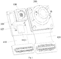
- Fig. 1 is a structural schematic diagram of the depth camera.
- the depth camera includes a laser emitting module 100 and a laser receiving module 200.
- the laser receiving module 200 and the laser emitting module 100 are arranged side by side.
- the laser emitting module 100 can change an angle of deviation of the laser beam, and thus, can adjust the irradiation direction of the laser beam, which is equivalent to realizing scanning of the laser beam within a certain angle, that is, increasing the field of view of the laser beam.
- the electric power of the laser emitting module 100 will not be increased, thus the overheating problem is solved, and the depth camera can operate for a long time.
- the electric power remains unchanged, the power consumption of the depth camera will not increase, and the power conversion efficiency will not decrease, so that the performance of the depth camera is ensured.
- the reason why the depth camera can increase the field of view of the laser beam without increasing the optical power of the laser beam is that the laser emitting module 100 can change the angle of deviation of the emitted laser beam, which will be explained below.
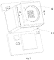
- Fig. 2 is a structural schematic diagram of the laser emitting module 100.
- the laser emitting module 100 may include an emitting assembly 11 and a laser deflection assembly 12.
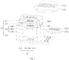
- Fig. 3 is a sectional view of Fig. 2 taken along line A-A.
- the emitting assembly 11 is provided with a beam outlet 11a, and the beam outlet 11a is configured to emit a laser beam.
- the laser deflection assembly 12 is located at the beam outlet 11a and is movable relative to the beam outlet 11a, the laser deflection assembly 12 is configured to change the angle of deviation of the laser beam emitted from the beam outlet 11a when the laser deflection assembly 12 is translated relative to the beam outlet 11a, and an included angle is formed between a translation direction of the laser deflection assembly 12 and a center line of the laser beam emitted from the beam outlet 11a.
- the laser beam is emitted from the beam outlet 11a of the emitting assembly 11 and passes through the laser deflection assembly 12.
- the laser deflection assembly 12 since the laser deflection assembly can change the angle of deviation of the laser beam by translating its position relative to the beam outlet, the irradiation direction of the laser beam can be adjusted, which is equivalent to realizing scanning of the laser beam within a certain angle, that is, increasing the field of view of the laser beam.
- the laser emitting module 100 does not increase the optical power of the laser beam in the process of increasing the field of view of the laser beam, the electric power of the laser emitting module 100 will not be increased, the overheating problem does not exist, and the depth camera can operate for a long time.
- an included angle is formed between the translation direction of the laser deflection assembly 12 and the center line of the laser beam emitted from the beam outlet 11a" means that the translation direction of the laser deflection assembly 12 is different from the direction of the center line of the laser beam emitted from the beam outlet 11a.
- the translation direction of the laser deflection assembly 12 may be perpendicular to the center line of the laser beam emitted from the beam outlet 11a. This design allows the laser deflection assembly 12 to be translated for a small distance to achieve large deflection of the laser beam.
- the laser deflection assembly 12 plays a key role in the process of increasing the field of view of the laser beam.
- the laser deflection assembly 12 will be further described below.
- the laser deflection assembly 12 may include a first lens array assembly 122 and a second lens array assembly 123.
- the first lens array assembly 122 is located at the beam outlet 11a, the second lens array assembly 123 is located at a side of the first lens array assembly 122 facing away from the emitting assembly 11, and the second lens array assembly 123 is capable of being translated relative to the first lens array assembly 122.
- the laser beam emitted from the emitting assembly 11 can be transmitted through the first lens array assembly 122 and the second lens array assembly 123 sequentially, and finally emitted out of the laser emitting module.
- the laser beam is transmitted through the first lens array assembly 122 and the second lens array assembly 123 sequentially, and the laser beam will not be deflected.
- the second lens array assembly is laterally translated relative to the first lens array assembly 122, since the position of the second lens array assembly 123 is deflected relative to the first lens array assembly 122, the laser beam will be deflected after being transmitted through the second lens array assembly 123.
- the angle of deviation of the laser beam also changes accordingly, so that the angle of deviation of the laser beam is controllable, that is, the field of view of the laser beam is controllable.
- the first lens array assembly 122 and the second lens array assembly 123 may be made of optical plastics or semiconductor materials, so that the first lens array assembly 122 and the second lens array assembly 123 can have good light transmittance and structural strength.
- the first lens array assembly 122 includes a first transparent plate 1221 and a plurality of first lens units 1222. More than one first lens units 1222 are connected to the first transparent plate 1221 and are arranged in an array, and an orthographic projection of the array formed by more than one first lens units 1222 on a plane where the beam outlet 11a is located at least partially overlaps with the beam outlet 11a.
- the second lens array assembly 123 includes a second transparent plate 1231 and a plurality of second lens units 1232. More than one second lens units 1232 are all connected to the second transparent plate 1231 and are arranged in an array, and an orthographic projection of the array formed by more than one second lens units 1232 on the plane where the beam outlet 11a is located at least partially overlaps with the beam outlet 11a.
- the second lens units 1232 are in one-to-one correspondence to the first lens units 1222, and an orthographic projection of the second lens unit 1232 on the first transparent plate 1221 at least partially overlaps with the corresponding first lens unit 1222.
- the first transparent plate 1221 and the second transparent plate 1231 both function as a carrier to respectively support the first lens units 1222 and the second lens units 1232.
- the laser beam is transmitted through the first lens units 1222 and split into a plurality of laser beams which are respectively emitted toward the corresponding second lens units 1232.
- the principal axis of the first lens unit 1222 overlaps with the principal axis of the corresponding second lens unit 1232, and the laser beam will not be deflected after being transmitted through the second lens unit 1232.
- the principal axes of the first lens unit 1222 and the corresponding second lens unit 1232 are spaced apart and in parallel, and the laser beam will be deflected after being transmitted through the second lens unit 1232.
- the first lens unit 1222 and the second lens unit 1232 may both be biconvex lenses, and the first lens unit 1222 and the second lens unit 1232 have the same radius.
- Such a design not only facilitates the design of the movement logic of the second lens array assembly 123, but also facilitates the centralized purchasing of the first lens units 1222 and the second lens units 1232, which is conducive to the control over the cost of the laser emitting module.
- the first lens unit 1222 has a radius of 10 ⁇ m-1 mm.
- the lateral translation stroke of the second lens array assembly 123 does not exceed the radius of the second lens unit 1232.
- the laser beam deflection formed within the lateral translation stroke can satisfy the demands for the field of view. If the lateral translation stroke of the second lens array assembly 123 is too large, it is not conducive to the miniaturization design of the laser emitting module.
- outer edges of the first lens unit 1222 and the second lens unit 1232 have the same shape, such as a circle, a quadrilateral, a hexagon, etc., which is not limited in the disclosure.
- the orthographic projection of the array formed by the plurality of first lens units 1222 on the plane where the beam outlet 11a is located at least partially overlaps with the beam outlet 11a. That is, the orthographic projection of the array formed by the plurality of first lens units 1222 on the plane where the beam outlet 11a is located may either include the beam outlet 11a or be included in the beam outlet 11a. The same is true for a projection relationship between the second lens units 1232 and the beam outlet 11a.
- orthographic projections of all the first lens units 1222 on the plane where the beam outlet 11a is located are located within the beam outlet 11a.
- Orthographic projections of all the second lens units 1232 on the plane where the beam outlet 11a is located is located within the beam outlet 11a.
- Such a design can prevent the beam outlet 11a from blocking the first lens units 1222 and the second lens units 1232.
- the first lens array assembly 122 can be located in the beam outlet 11a, so that the structure of the laser emitting module is more compact, which is conducive to the miniaturization design.
- the beam outlet 11a is located within the orthographic projection of the array formed by the plurality of first lens units 1222 on the plane where the beam outlet 11a is located, and the beam outlet 11a is located within the orthographic projection of the array formed by the plurality of second lens units 1232 on the plane where the beam outlet 11a is located.
- Such a design can prevent the laser beam from exuding from the processing range of the first lens units 1222 and the second lens units 1232.
- the laser deflection assembly 12 further includes a circuit board assembly 124 and an actuator 121.
- the circuit board assembly 124 is located outside the beam outlet 11a and is connected to the emitting assembly 11.
- the actuator 121 is located at a side of the circuit board assembly 124 facing away from the emitting assembly 11 and is connected to the circuit board assembly 124, an actuation direction of the actuator 121 is perpendicular to the center line of the laser beam emitted from the beam outlet 11a, and the second lens array assembly 123 is connected to the actuator 121.
- the circuit board assembly 124 serves as a carrier of the actuator 121 and provides electric power for the actuator 121, so that the actuator 121 can drive the second lens array assembly 123 to move in the actuation direction.
- the actuation direction refers to the direction in which the actuator 121 can drive the component to move.
- the actuator 121 may be any one of a voice coil motor, a micro-electro-mechanical system motor, a shape memory alloy motor and an ultrasonic motor.
- micro-actuators such as the voice coil motor (VCM), the micro-electro-mechanical system (MEMS) motor, the shape memory alloy (SMA) motor and the ultrasonic motor (USM) are adopted, and by utilizing its extremely small size, the occupied space can be reduced, and the second lens array assembly 123 can be effectively driven.
- VCM voice coil motor
- MEMS micro-electro-mechanical system
- SMA shape memory alloy
- USM ultrasonic motor
- the voice coil motor has a similar operating principle to a loudspeaker, and has the characteristics of high frequency response and high accuracy.
- the main principle of the voice coil motor is to control the stretching position of a leaf spring by changing the magnitude of the direct current of the coil in the voice coil motor in a permanent magnetic field, thereby driving the leaf spring to reciprocate in a certain direction (actuation direction).
- the actuator 121 is a voice coil motor
- the second lens array assembly 123 is located inside the actuator 121, and the outer edge of the second lens array assembly 123 is connected to the leaf spring, so that the lateral movement of the second lens array assembly 123 is driven by the reciprocation of the leaf spring.
- the operating principle of the shape memory alloy motor is to generate actuation by using the expansion and contraction characteristics of shape memory alloy.
- the expansion and contraction direction is the actuation direction.
- the actuator 121 is a shape memory alloy motor
- the second lens array assembly 123 is located inside the actuator 121, and the outer edge of the second lens array assembly 123 is connected to the shape memory alloy, so that the lateral movement of the second lens array assembly 123 is driven by the expansion and contraction of the shape memory alloy.
- the circuit board assembly 124 includes a first circuit board 1241 and a second circuit board 1242.
- the first circuit board 1241 is sandwiched between the actuator 121 and the beam outlet 11a, the middle of the first circuit board 1241 is provided with a light transmitting hole 1241a, and the light transmitting hole 1241a is opposite to the beam outlet 11a.
- One end of the second circuit board 1242 is connected to the first circuit board 1241, and the other end of the second circuit board 1242 is connected to the emitting assembly 11.
- the first circuit board 1241 is configured to carry the actuator 121 and provide electric power for the actuator 121.
- the first circuit board 1241 With the connection of the second circuit board 1242, the first circuit board 1241 can be connected to the emitting assembly 11, so that the emitting assembly 11 can be used to provide electric power for the first circuit board 1241, and thus, the structure of the laser emitting module 100 is more compact, which is conducive to the miniaturization design of the depth camera.
- the first circuit board 1241 may be a printed circuit board, and the second circuit board 1242 may be a flexible circuit board.
- the actuator 121 can be carried more stably due to the structural strength of the printed circuit board, and the first circuit board 1241 can be connected to the emitting assembly 11 conveniently due to the flexibility of the flexible circuit board.
- the second circuit board 1242 is located outside the emitting assembly 11, which can thereby prevent the second circuit board 1242 from affecting the normal operation of the emitting assembly 11.
- the emitting assembly 11 may include a third circuit board 111, a frame 112 and a laser chip 113.
- One end of the frame 112 is connected to a surface of the third circuit board 111, and the other end of the frame 112 is provided with the beam outlet 11a.
- the laser chip 113 is located in the frame 112 and is connected to the surface of the third circuit board 111.
- the third circuit board 111 is configured to carry the frame 112 and the laser chip 113 and provide electric power for the laser chip 113.
- the frame 112 is hollow inside, and is configured to accommodate the laser chip 113.
- the laser chip 113 is configured to emit the laser beam, so that the laser beam penetrates through the space inside the frame 112 and is emitted from the beam outlet 11a.
- the third circuit board 111 may be a printed circuit board.
- the frame 112 and the laser chip 113 can be carried more stably due to the structural strength of the printed circuit board.
- the laser chip 113 may be a vertical-cavity surface-emitting laser (VCSEL).
- the laser chip 113 includes a substrate and a chip body. One surface of the substrate is connected to the third circuit board 111, and the other surface of the substrate is connected to the chip body.
- both a laser chip driver 1131 and an actuator driver 125 are connected to the third circuit board 111 and located on the same side of a bracket 22.
- Such a design can make the structure of the laser emitting module 100 more compact, which is conducive to the miniaturization design of the depth camera.
- the emitting assembly 11 further includes a collimating lens 114.
- the collimating lens 114 is located between the beam outlet 11a and the laser chip 113, and the collimating lens 114 is connected to the inner wall of the frame 112.
- the laser beam is collimated by the collimating lens 114 before being emitted from the beam outlet 11a, so that all the laser beams emitted from the beam outlet 11a are collimated laser beams.
- the interference of the laser beams can be better controlled.
- Fig. 4 is a schematic diagram of a light path of the laser beam. The operating process of the laser emitting module 100 will be described below with reference to Fig. 4 .
- the laser beam is emitted by the laser chip 113, collimated by the collimating lens 114, and then emitted out of the emitting assembly 11 from the beam outlet 11a.
- the laser beam emitted out of the emitting assembly 11 is transmitted through the corresponding first lens unit 1222 and second lens unit 1232 sequentially.
- the principal axis of the first lens unit 1222 overlaps with the principal axis of the corresponding second lens unit 1232, and the laser beam will not be deflected after being transmitted through the second lens unit 1232 (with reference to the upper part of Fig. 4 ).
- the principal axes of the first lens unit 1222 and the corresponding second lens unit 1232 are spaced apart and in parallel, and the laser beam will be deflected leftwards after being transmitted through the second lens unit 1232.
- 0 is the angle of deviation of the laser beam
- x is the transversal displacement stroke of the second lens array assembly 123
- p is the distance between the corresponding first lens unit 1222 and second lens unit 1232
- FNO is the F-number of a focusing lens (not shown).
- the focusing lens is one of other components of the depth camera, and is configured to focus the laser beam transmitted through the second lens array assembly 123.
- the angle of deviation of the laser beam can be controlled by controlling the transversal displacement stroke of the second lens array assembly 123.
- the laser receiving module 200 will be described below.
- Fig. 5 is a sectional view of Fig. 1 taken along line B-B.
- the laser receiving module 200 includes a fourth circuit board 21, a bracket 22 and a sensor chip 23.
- the bracket 22 is connected to a surface of the fourth circuit board 21, the bracket 22 is provided with a beam inlet 22a, the beam inlet 22a is located on a surface of the bracket 22 facing away from the fourth circuit board 21, and the beam inlet 22a and the beam outlet 11a have the same orientation.
- the sensor chip 23 is located within the bracket 22 and is connected to the surface of the fourth circuit board 21, and the sensor chip 23 is opposite to the beam inlet 22a.
- the fourth circuit board 21 is configured to carry the bracket 22 and the sensor chip 23 and provide electric power for the sensor chip 23.
- the sensor chip 23 is configured to receive a laser beam entering from the beam inlet 22a, thereby calculating the depth of field.
- the bracket 22 covers the outside of the sensor chip 23, and is configured to support other components and protect the sensor chip 23.
- the fourth circuit board 21 may be a printed circuit board.
- the bracket 22 and the sensor chip 23 can be carried more stably due to the structural strength of the printed circuit board.
- the laser receiving module 200 may further include a receiving lens 24 and a narrowband filter 25.
- the receiving lens 24 is located at the beam inlet 22a and is connected to the bracket 22.
- the narrowband filter 25 is located at the beam inlet 22a and is sandwiched between the receiving lens 24 and the bracket 22.
- the receiving lens 24 is configured to converge the reflected laser beam, so that the laser beam can pass through the narrowband filter 25, enter the bracket 22 from the beam inlet 22a after being filtered, and thus be sensed by the sensor chip 23.
- the depth camera further includes a reinforcing plate 300.
- the laser emitting module 100 and the laser receiving module 200 are connected to the same surface of the reinforcing plate 300.
- the reinforcing plate 300 is configured to reinforce the third circuit board 111 and the fourth circuit board 21, thereby improving the structural strength of the third circuit board 111 and the fourth circuit board 21 and further improving the structural strength of the depth camera.
- the laser emitting module 100 and the laser receiving module 200 respectively extend to form a first flexible circuit board 410 and a second flexible circuit board 420 so as to serve as a connector, which thereby facilitates the connection with the other components in the depth camera.
- the first flexible circuit board 410 extending from the laser emitting module 100 is connected to the third circuit board 111, and the second flexible circuit board 420 extending from the laser receiving module 200 is connected to the fourth circuit board 21.
- the first flexible circuit board 410 extending from the laser emitting module 100 and the second flexible circuit board 420 extending from the laser receiving module 200 are located on the same side. Such a design can make the structure more compact, which is conducive to the miniaturization design of the depth camera.
- the depth camera provided by the embodiments of the disclosure can satisfy the requirements on large deflection angle, high scanning rate, high pointing accuracy, low loss, low power consumption and high stability.
- a laser beam can be pointed randomly within a larger field of view, and the laser beam can be deflected from one angle to another angle with a small increment, and can stay on the target object for a required time.
- Fig. 6 is a structural schematic diagram of an electronic device according to the embodiments of the disclosure.
- the electronic device may be a mobile phone, a tablet computer or the like.
- the electronic device includes a shell 1000 and a depth camera 2000.
- the depth camera 2000 is the depth camera shown in Fig. 1-5 , and the depth camera 2000 is located in the shell 1000.
- the electronic device includes the depth camera shown in Fig. 1-5 , and thus, can have all the beneficial effects of the depth camera, which will not be repeated here.
Landscapes
- Physics & Mathematics (AREA)
- General Physics & Mathematics (AREA)
- Engineering & Computer Science (AREA)
- Optics & Photonics (AREA)
- Computer Networks & Wireless Communication (AREA)
- Remote Sensing (AREA)
- Radar, Positioning & Navigation (AREA)
- Electromagnetism (AREA)
- Condensed Matter Physics & Semiconductors (AREA)
- General Health & Medical Sciences (AREA)
- Theoretical Computer Science (AREA)
- Multimedia (AREA)
- Vascular Medicine (AREA)
- Health & Medical Sciences (AREA)
- Semiconductor Lasers (AREA)
Abstract
Description
- A depth camera, belonging to a 3D camera, can detect the depth of field of a shooting space.
- In the related art, a depth camera mainly includes a laser emitting module and a laser receiving module. The laser emitting module is used to emit a laser beam to a target object, and the laser receiving module is used to receive the reflected laser beam. In order to increase the field of view of the emitted laser beam, it is necessary to increase the optical power of the laser beam, that is, increase the electric power of the laser emitting module.
- However, as the electric power of the laser emitting module increases, the laser emitting module will generate more heat, which brings up higher requirements on the heat dissipation performance of the depth camera and is not conducive to the long-time operation of the depth camera.
- In order to solve the above technical problems, an objective of the disclosure is to provide a laser emitting module, a depth camera and an electronic device that can increase the field of view of an emitted laser beam.
- According to a first aspect of the disclosure, a laser emitting module is provided, and including:
- an emitting assembly has a beam outlet, and the beam outlet is configured to emit a laser beam;
- a laser deflection assembly is at the beam outlet and is movable relative to the beam outlet, the laser deflection assembly is configured to change an angle of deviation of the laser beam emitted from the beam outlet when the laser deflection assembly is translated relative to the beam outlet, and an included angle is between a translation direction of the laser deflection assembly and a center line of the laser beam emitted from the beam outlet.
- Optionally, the laser deflection assembly includes a first lens array assembly and a second lens array assembly;
- the first lens array assembly is at the beam outlet; and
- the second lens array assembly is at a side of the first lens array assembly facing away from the emitting assembly, and the second lens array assembly can be translated relative to the first lens array assembly.
- Optionally, the first lens array assembly includes a first transparent plate and a plurality of first lens units;
- more than one first lens units are connected to the first transparent plate and are arranged in an array, and an orthographic projection of the array formed by more than one first lens units on a plane where the beam outlet is located at least partially overlaps with the beam outlet;
- the second lens array assembly includes a second transparent plate and a plurality of second lens units;
- more than one second lens units are connected to the second transparent plate and are arranged in an array, and an orthographic projection of the array formed by more than one second lens units on the plane where the beam outlet is located at least partially overlaps with the beam outlet; and
- the second lens units are in a one-to-one correspondence to the first lens units, and an orthographic projection of the second lens unit on the first transparent plate at least partially overlaps with the corresponding first lens unit.
- Optionally, orthographic projections of all the first lens units on the plane where the beam outlet is located are within the beam outlet; and
orthographic projections of all the second lens units on the plane where the beam outlet is located are within the beam outlet. - Optionally, the laser deflection assembly further includes a circuit board assembly and an actuator;
- the circuit board assembly is outside the beam outlet and is connected to the emitting assembly;
- the actuator is at a side of the circuit board assembly facing away from the emitting assembly and is connected to the circuit board assembly, and an actuation direction of the actuator is perpendicular to the center line of the laser beam emitted from the beam outlet; and
- the second lens array assembly is connected to the actuator.
- Optionally, the actuator is any one of a voice coil motor, a micro-electro-mechanical system motor, a shape memory alloy motor and an ultrasonic motor.
- Optionally, the circuit board assembly includes a first circuit board and a second circuit board;
- the first circuit board is sandwiched between the actuator and the beam outlet, a light transmitting hole is in a middle of the first circuit board, and the light transmitting hole is opposite to the beam outlet; and
- one end of the second circuit board is connected to the first circuit board, and the other end of the second circuit board is connected to the emitting assembly.
- Optionally, the emitting assembly includes a third circuit board, a frame and a laser chip;
- one end of the frame is connected to a surface of the third circuit board, and the other end of the frame has the beam outlet; and
- the laser chip is in the frame and is connected to the surface of the third circuit board.
- Optionally, the emitting assembly further includes a collimating lens; and
the collimating lens is between the beam outlet and the laser chip, and the collimating lens is connected to an inner wall of the frame. - According to a second aspect of the disclosure, a depth camera is provided, and including:
- a laser emitting module according to the first aspect of the disclosure; and
- a laser receiving module, arranged side by side with the laser emitting module.
- Optionally, the laser receiving module includes a fourth circuit board, a bracket and a sensor chip;
- the bracket is connected to a surface of the fourth circuit board, the bracket has a beam inlet, the beam inlet is on a surface of the bracket facing away from the fourth circuit board, and the beam inlet and the beam outlet have the same orientation; and
- the sensor chip is in the bracket and is connected to the surface of the fourth circuit board, and the sensor chip is opposite to the beam inlet.
- Optionally, the laser receiving module further includes a receiving lens and a narrowband filter;
- the receiving lens is at the beam inlet and is connected to the bracket; and
- the narrowband filter is at the beam inlet and is sandwiched between the receiving lens and the bracket.
- According to a third aspect of the disclosure, an electronic device is provided, and including:
- a shell; and
- a depth camera according to the second aspect of the disclosure, and the depth camera is in the shell.
- The technical solutions provided by the examples of the disclosure at least have the following beneficial effects:
When the laser emitting module provided by the examples of the disclosure is used to emit the laser beam, the laser beam is emitted from the beam outlet of the emitting assembly and passes through the laser deflection assembly. When the laser beam passes through the laser deflection assembly, since the laser deflection assembly can change the angle of deviation of the laser beam by translating its position relative to the beam outlet, the irradiation direction of the laser beam can be adjusted, which is equivalent to realizing scanning of the laser beam within a certain angle, that is, increasing the field of view of the laser beam. - Besides, since the laser emitting module provided by the examples of the disclosure does not increase the optical power of the laser beam in the process of increasing the field of view of the laser beam, the electric power of the laser emitting module will not be increased, the overheating problem does not exist, and the depth camera can operate for a long time.
- In order to illustrate the technical solutions in some embodiments of the disclosure, the accompanying drawings required in the description of embodiments will be briefly described below. The accompanying drawings in the description below are some embodiments of the disclosure, and those of ordinary skill in the art can obtain other accompanying drawings according to these drawings without any creative work.
-
Fig. 1 is a structural schematic diagram of a depth camera according to an embodiment of the disclosure; -
Fig. 2 is a structural schematic diagram of a laser emitting module according to an embodiment of the disclosure; -
Fig. 3 is a sectional view ofFig. 2 taken along line A-A according to an embodiment of the disclosure; -
Fig. 4 is a schematic diagram of a light path of a laser beam according to an embodiment of the disclosure; -
Fig. 5 is a sectional view ofFig. 1 taken along line B-B according to an embodiment of the disclosure; and -
Fig. 6 is a structural schematic diagram of an electronic device according to an embodiment of the disclosure. - In order to make the objectives, technical solutions and advantages of the disclosure clearer, the embodiments of the disclosure will be described in further detail below in conjunction with the accompanying drawings.
- A depth camera, belonging to a 3D camera, can detect the depth of field of a shooting space.
- In the related art, depth cameras mainly include the following three types: structured light depth cameras, binocular stereo vision depth cameras and optical time-of-flight depth cameras.
- The optical time-of-flight depth camera refers to the TOF (Time of flight) camera, mainly including a laser emitting module and a laser receiving module. The laser emitting module is configured to emit a laser beam to a target object, and the laser receiving module is configured to receive the reflected laser beam. The time difference between the emitted laser beam and the received laser beam is used to calculate the depth of field of the target object. In order to make the laser beam irradiate more target objects, the field of view of the emitted laser beam needs to be increased, and thus, the optical power of the laser beam needs to be increased, that is, the electric power of the laser emitting module is increased.
- However, as the electric power of the laser emitting module increases, the laser emitting module will generate more heat, which brings up higher requirements on the heat dissipation performance of the depth camera and is not conducive to the long-time operation of the depth camera.
- In order to solve the above technical problems, embodiments of the disclosure provide a depth camera.
Fig. 1 is a structural schematic diagram of the depth camera. As shown inFig. 1 , the depth camera includes alaser emitting module 100 and alaser receiving module 200. Thelaser receiving module 200 and thelaser emitting module 100 are arranged side by side. Thelaser emitting module 100 can change an angle of deviation of the laser beam, and thus, can adjust the irradiation direction of the laser beam, which is equivalent to realizing scanning of the laser beam within a certain angle, that is, increasing the field of view of the laser beam. - Besides, since changing the angle of deviation of the laser beam does not need to increase the optical power of the laser beam, the electric power of the
laser emitting module 100 will not be increased, thus the overheating problem is solved, and the depth camera can operate for a long time. In addition, when the electric power remains unchanged, the power consumption of the depth camera will not increase, and the power conversion efficiency will not decrease, so that the performance of the depth camera is ensured. - As mentioned above, it can be known that the reason why the depth camera can increase the field of view of the laser beam without increasing the optical power of the laser beam is that the
laser emitting module 100 can change the angle of deviation of the emitted laser beam, which will be explained below. -
Fig. 2 is a structural schematic diagram of thelaser emitting module 100. With reference toFig. 2 , in an embodiment, thelaser emitting module 100 may include an emittingassembly 11 and alaser deflection assembly 12. -
Fig. 3 is a sectional view ofFig. 2 taken along line A-A. With reference toFig. 3 , the emittingassembly 11 is provided with a beam outlet 11a, and the beam outlet 11a is configured to emit a laser beam. Thelaser deflection assembly 12 is located at the beam outlet 11a and is movable relative to the beam outlet 11a, thelaser deflection assembly 12 is configured to change the angle of deviation of the laser beam emitted from the beam outlet 11a when thelaser deflection assembly 12 is translated relative to the beam outlet 11a, and an included angle is formed between a translation direction of thelaser deflection assembly 12 and a center line of the laser beam emitted from the beam outlet 11a. - When the
laser emitting module 100 according to the disclosure is used to emit the laser beam, the laser beam is emitted from the beam outlet 11a of the emittingassembly 11 and passes through thelaser deflection assembly 12. When the laser beam passes through thelaser deflection assembly 12, since the laser deflection assembly can change the angle of deviation of the laser beam by translating its position relative to the beam outlet, the irradiation direction of the laser beam can be adjusted, which is equivalent to realizing scanning of the laser beam within a certain angle, that is, increasing the field of view of the laser beam. - Besides, since the
laser emitting module 100 according to the disclosure does not increase the optical power of the laser beam in the process of increasing the field of view of the laser beam, the electric power of thelaser emitting module 100 will not be increased, the overheating problem does not exist, and the depth camera can operate for a long time. - It should be noted that "an included angle is formed between the translation direction of the
laser deflection assembly 12 and the center line of the laser beam emitted from the beam outlet 11a" means that the translation direction of thelaser deflection assembly 12 is different from the direction of the center line of the laser beam emitted from the beam outlet 11a. In an embodiment of the disclosure, the translation direction of thelaser deflection assembly 12 may be perpendicular to the center line of the laser beam emitted from the beam outlet 11a. This design allows thelaser deflection assembly 12 to be translated for a small distance to achieve large deflection of the laser beam. - It can be seen that the
laser deflection assembly 12 plays a key role in the process of increasing the field of view of the laser beam. Thelaser deflection assembly 12 will be further described below. - Referring to
Fig. 3 , in an embodiment, thelaser deflection assembly 12 may include a firstlens array assembly 122 and a secondlens array assembly 123. - The first
lens array assembly 122 is located at the beam outlet 11a, the secondlens array assembly 123 is located at a side of the firstlens array assembly 122 facing away from the emittingassembly 11, and the secondlens array assembly 123 is capable of being translated relative to the firstlens array assembly 122. - In the above embodiment, since the first
lens array assembly 122 is located in the beam outlet 11a and the secondlens array assembly 123 is located at the side of the firstlens array assembly 122 facing away from the emittingassembly 11, the laser beam emitted from the emittingassembly 11 can be transmitted through the firstlens array assembly 122 and the secondlens array assembly 123 sequentially, and finally emitted out of the laser emitting module. - When the second
lens array assembly 123 is in the original position, the laser beam is transmitted through the firstlens array assembly 122 and the secondlens array assembly 123 sequentially, and the laser beam will not be deflected. When the second lens array assembly is laterally translated relative to the firstlens array assembly 122, since the position of the secondlens array assembly 123 is deflected relative to the firstlens array assembly 122, the laser beam will be deflected after being transmitted through the secondlens array assembly 123. As the movement stroke of the secondlens array assembly 123 changes, the angle of deviation of the laser beam also changes accordingly, so that the angle of deviation of the laser beam is controllable, that is, the field of view of the laser beam is controllable. - In some embodiments, the first
lens array assembly 122 and the secondlens array assembly 123 may be made of optical plastics or semiconductor materials, so that the firstlens array assembly 122 and the secondlens array assembly 123 can have good light transmittance and structural strength. - Referring to
Fig. 3 , in an embodiment, the firstlens array assembly 122 includes a firsttransparent plate 1221 and a plurality offirst lens units 1222. More than onefirst lens units 1222 are connected to the firsttransparent plate 1221 and are arranged in an array, and an orthographic projection of the array formed by more than onefirst lens units 1222 on a plane where the beam outlet 11a is located at least partially overlaps with the beam outlet 11a. - The second
lens array assembly 123 includes a secondtransparent plate 1231 and a plurality ofsecond lens units 1232. More than onesecond lens units 1232 are all connected to the secondtransparent plate 1231 and are arranged in an array, and an orthographic projection of the array formed by more than onesecond lens units 1232 on the plane where the beam outlet 11a is located at least partially overlaps with the beam outlet 11a. - The
second lens units 1232 are in one-to-one correspondence to thefirst lens units 1222, and an orthographic projection of thesecond lens unit 1232 on the firsttransparent plate 1221 at least partially overlaps with the correspondingfirst lens unit 1222. - In the above embodiment, the first
transparent plate 1221 and the secondtransparent plate 1231 both function as a carrier to respectively support thefirst lens units 1222 and thesecond lens units 1232. After being emitted from the beam outlet 11a, the laser beam is transmitted through thefirst lens units 1222 and split into a plurality of laser beams which are respectively emitted toward the correspondingsecond lens units 1232. When the secondlens array assembly 123 is in the original position, the principal axis of thefirst lens unit 1222 overlaps with the principal axis of the correspondingsecond lens unit 1232, and the laser beam will not be deflected after being transmitted through thesecond lens unit 1232. After the secondlens array assembly 123 is moved laterally, the principal axes of thefirst lens unit 1222 and the correspondingsecond lens unit 1232 are spaced apart and in parallel, and the laser beam will be deflected after being transmitted through thesecond lens unit 1232. - In some embodiments, the
first lens unit 1222 and thesecond lens unit 1232 may both be biconvex lenses, and thefirst lens unit 1222 and thesecond lens unit 1232 have the same radius. Such a design not only facilitates the design of the movement logic of the secondlens array assembly 123, but also facilitates the centralized purchasing of thefirst lens units 1222 and thesecond lens units 1232, which is conducive to the control over the cost of the laser emitting module. Thefirst lens unit 1222 has a radius of 10 µm-1 mm. - Based on the original position, the lateral translation stroke of the second
lens array assembly 123 does not exceed the radius of thesecond lens unit 1232. The laser beam deflection formed within the lateral translation stroke can satisfy the demands for the field of view. If the lateral translation stroke of the secondlens array assembly 123 is too large, it is not conducive to the miniaturization design of the laser emitting module. - In some embodiments, outer edges of the
first lens unit 1222 and thesecond lens unit 1232 have the same shape, such as a circle, a quadrilateral, a hexagon, etc., which is not limited in the disclosure. - It can be known that the orthographic projection of the array formed by the plurality of
first lens units 1222 on the plane where the beam outlet 11a is located at least partially overlaps with the beam outlet 11a. That is, the orthographic projection of the array formed by the plurality offirst lens units 1222 on the plane where the beam outlet 11a is located may either include the beam outlet 11a or be included in the beam outlet 11a. The same is true for a projection relationship between thesecond lens units 1232 and the beam outlet 11a. - In some embodiments, orthographic projections of all the
first lens units 1222 on the plane where the beam outlet 11a is located are located within the beam outlet 11a. Orthographic projections of all thesecond lens units 1232 on the plane where the beam outlet 11a is located is located within the beam outlet 11a. Such a design can prevent the beam outlet 11a from blocking thefirst lens units 1222 and thesecond lens units 1232. In such cases, the firstlens array assembly 122 can be located in the beam outlet 11a, so that the structure of the laser emitting module is more compact, which is conducive to the miniaturization design. - In other embodiments, the beam outlet 11a is located within the orthographic projection of the array formed by the plurality of
first lens units 1222 on the plane where the beam outlet 11a is located, and the beam outlet 11a is located within the orthographic projection of the array formed by the plurality ofsecond lens units 1232 on the plane where the beam outlet 11a is located. Such a design can prevent the laser beam from exuding from the processing range of thefirst lens units 1222 and thesecond lens units 1232. - Referring to
Fig. 3 , in an embodiment, thelaser deflection assembly 12 further includes acircuit board assembly 124 and anactuator 121. Thecircuit board assembly 124 is located outside the beam outlet 11a and is connected to the emittingassembly 11. Theactuator 121 is located at a side of thecircuit board assembly 124 facing away from the emittingassembly 11 and is connected to thecircuit board assembly 124, an actuation direction of theactuator 121 is perpendicular to the center line of the laser beam emitted from the beam outlet 11a, and the secondlens array assembly 123 is connected to theactuator 121. - In the above embodiment, the
circuit board assembly 124 serves as a carrier of theactuator 121 and provides electric power for theactuator 121, so that theactuator 121 can drive the secondlens array assembly 123 to move in the actuation direction. The actuation direction refers to the direction in which theactuator 121 can drive the component to move. - In some embodiments, the
actuator 121 may be any one of a voice coil motor, a micro-electro-mechanical system motor, a shape memory alloy motor and an ultrasonic motor. - In the above embodiment, micro-actuators, such as the voice coil motor (VCM), the micro-electro-mechanical system (MEMS) motor, the shape memory alloy (SMA) motor and the ultrasonic motor (USM) are adopted, and by utilizing its extremely small size, the occupied space can be reduced, and the second
lens array assembly 123 can be effectively driven. - For example, the voice coil motor has a similar operating principle to a loudspeaker, and has the characteristics of high frequency response and high accuracy. The main principle of the voice coil motor is to control the stretching position of a leaf spring by changing the magnitude of the direct current of the coil in the voice coil motor in a permanent magnetic field, thereby driving the leaf spring to reciprocate in a certain direction (actuation direction). When the
actuator 121 is a voice coil motor, the secondlens array assembly 123 is located inside theactuator 121, and the outer edge of the secondlens array assembly 123 is connected to the leaf spring, so that the lateral movement of the secondlens array assembly 123 is driven by the reciprocation of the leaf spring. - The operating principle of the shape memory alloy motor is to generate actuation by using the expansion and contraction characteristics of shape memory alloy. The expansion and contraction direction is the actuation direction. When the
actuator 121 is a shape memory alloy motor, the secondlens array assembly 123 is located inside theactuator 121, and the outer edge of the secondlens array assembly 123 is connected to the shape memory alloy, so that the lateral movement of the secondlens array assembly 123 is driven by the expansion and contraction of the shape memory alloy. - In order to control the
actuator 121, in some embodiments, thecircuit board assembly 124 includes afirst circuit board 1241 and asecond circuit board 1242. - The
first circuit board 1241 is sandwiched between the actuator 121 and the beam outlet 11a, the middle of thefirst circuit board 1241 is provided with alight transmitting hole 1241a, and thelight transmitting hole 1241a is opposite to the beam outlet 11a. One end of thesecond circuit board 1242 is connected to thefirst circuit board 1241, and the other end of thesecond circuit board 1242 is connected to the emittingassembly 11. - In the above embodiment, the
first circuit board 1241 is configured to carry theactuator 121 and provide electric power for theactuator 121. With the connection of thesecond circuit board 1242, thefirst circuit board 1241 can be connected to the emittingassembly 11, so that the emittingassembly 11 can be used to provide electric power for thefirst circuit board 1241, and thus, the structure of thelaser emitting module 100 is more compact, which is conducive to the miniaturization design of the depth camera. - In some embodiments, the
first circuit board 1241 may be a printed circuit board, and thesecond circuit board 1242 may be a flexible circuit board. Thus, theactuator 121 can be carried more stably due to the structural strength of the printed circuit board, and thefirst circuit board 1241 can be connected to the emittingassembly 11 conveniently due to the flexibility of the flexible circuit board. - In some embodiments, the
second circuit board 1242 is located outside the emittingassembly 11, which can thereby prevent thesecond circuit board 1242 from affecting the normal operation of the emittingassembly 11. - How the laser beam is deflected by the
laser deflection assembly 12 has been described above, and the emittingassembly 11 will be described below. - Referring to
Fig. 3 , in an embodiment, the emittingassembly 11 may include athird circuit board 111, aframe 112 and alaser chip 113. - One end of the
frame 112 is connected to a surface of thethird circuit board 111, and the other end of theframe 112 is provided with the beam outlet 11a. Thelaser chip 113 is located in theframe 112 and is connected to the surface of thethird circuit board 111. - In the above embodiment, the
third circuit board 111 is configured to carry theframe 112 and thelaser chip 113 and provide electric power for thelaser chip 113. Theframe 112 is hollow inside, and is configured to accommodate thelaser chip 113. Thelaser chip 113 is configured to emit the laser beam, so that the laser beam penetrates through the space inside theframe 112 and is emitted from the beam outlet 11a. - In some embodiments, the
third circuit board 111 may be a printed circuit board. Thus, theframe 112 and thelaser chip 113 can be carried more stably due to the structural strength of the printed circuit board. - In some embodiments, the
laser chip 113 may be a vertical-cavity surface-emitting laser (VCSEL). Thelaser chip 113 includes a substrate and a chip body. One surface of the substrate is connected to thethird circuit board 111, and the other surface of the substrate is connected to the chip body. - In some embodiments, both a
laser chip driver 1131 and anactuator driver 125 are connected to thethird circuit board 111 and located on the same side of abracket 22. Such a design can make the structure of thelaser emitting module 100 more compact, which is conducive to the miniaturization design of the depth camera. - In order to ensure all the laser beams emitted from the beam outlet 11a are collimated laser beams, in an embodiment, the emitting
assembly 11 further includes acollimating lens 114. Thecollimating lens 114 is located between the beam outlet 11a and thelaser chip 113, and thecollimating lens 114 is connected to the inner wall of theframe 112. With such a design, the laser beam is collimated by thecollimating lens 114 before being emitted from the beam outlet 11a, so that all the laser beams emitted from the beam outlet 11a are collimated laser beams. Thus, the interference of the laser beams can be better controlled. -
Fig. 4 is a schematic diagram of a light path of the laser beam. The operating process of thelaser emitting module 100 will be described below with reference toFig. 4 . - The laser beam is emitted by the
laser chip 113, collimated by thecollimating lens 114, and then emitted out of the emittingassembly 11 from the beam outlet 11a. The laser beam emitted out of the emittingassembly 11 is transmitted through the correspondingfirst lens unit 1222 andsecond lens unit 1232 sequentially. When the secondlens array assembly 123 is in the original position, the principal axis of thefirst lens unit 1222 overlaps with the principal axis of the correspondingsecond lens unit 1232, and the laser beam will not be deflected after being transmitted through the second lens unit 1232 (with reference to the upper part ofFig. 4 ). After the secondlens array assembly 123 is moved laterally (slightly moved leftwards inFig. 4 ), the principal axes of thefirst lens unit 1222 and the correspondingsecond lens unit 1232 are spaced apart and in parallel, and the laser beam will be deflected leftwards after being transmitted through thesecond lens unit 1232. - According to the geometric relationship, the following relationship is satisfied between the lateral displacement stroke of the second
lens array assembly 123 and the angle of deviation of the laser beam:
- 0 is the angle of deviation of the laser beam, x is the transversal displacement stroke of the second
lens array assembly 123, p is the distance between the correspondingfirst lens unit 1222 andsecond lens unit 1232, and FNO is the F-number of a focusing lens (not shown). The focusing lens is one of other components of the depth camera, and is configured to focus the laser beam transmitted through the secondlens array assembly 123. - It can be seen that under the condition that the distance between the corresponding
first lens unit 1222 andsecond lens unit 1232 and the F-number of the focusing lens remain unchanged, the angle of deviation of the laser beam can be controlled by controlling the transversal displacement stroke of the secondlens array assembly 123. - The
laser receiving module 200 will be described below. -
Fig. 5 is a sectional view ofFig. 1 taken along line B-B. With reference toFig. 5 , in an embodiment, thelaser receiving module 200 includes afourth circuit board 21, abracket 22 and asensor chip 23. - The
bracket 22 is connected to a surface of thefourth circuit board 21, thebracket 22 is provided with abeam inlet 22a, thebeam inlet 22a is located on a surface of thebracket 22 facing away from thefourth circuit board 21, and thebeam inlet 22a and the beam outlet 11a have the same orientation. Thesensor chip 23 is located within thebracket 22 and is connected to the surface of thefourth circuit board 21, and thesensor chip 23 is opposite to thebeam inlet 22a. - In the above embodiment, the
fourth circuit board 21 is configured to carry thebracket 22 and thesensor chip 23 and provide electric power for thesensor chip 23. Thesensor chip 23 is configured to receive a laser beam entering from thebeam inlet 22a, thereby calculating the depth of field. Thebracket 22 covers the outside of thesensor chip 23, and is configured to support other components and protect thesensor chip 23. - In some embodiments, the
fourth circuit board 21 may be a printed circuit board. Thus, thebracket 22 and thesensor chip 23 can be carried more stably due to the structural strength of the printed circuit board. - In some embodiments, the
laser receiving module 200 may further include a receivinglens 24 and anarrowband filter 25. - The receiving
lens 24 is located at thebeam inlet 22a and is connected to thebracket 22. Thenarrowband filter 25 is located at thebeam inlet 22a and is sandwiched between the receivinglens 24 and thebracket 22. - The receiving
lens 24 is configured to converge the reflected laser beam, so that the laser beam can pass through thenarrowband filter 25, enter thebracket 22 from thebeam inlet 22a after being filtered, and thus be sensed by thesensor chip 23. - Referring to
Fig. 1 , in an embodiment, the depth camera further includes a reinforcingplate 300. Thelaser emitting module 100 and thelaser receiving module 200 are connected to the same surface of the reinforcingplate 300. - In the above embodiment, the reinforcing
plate 300 is configured to reinforce thethird circuit board 111 and thefourth circuit board 21, thereby improving the structural strength of thethird circuit board 111 and thefourth circuit board 21 and further improving the structural strength of the depth camera. - In some embodiments, the
laser emitting module 100 and thelaser receiving module 200 respectively extend to form a firstflexible circuit board 410 and a secondflexible circuit board 420 so as to serve as a connector, which thereby facilitates the connection with the other components in the depth camera. - In some embodiments, the first
flexible circuit board 410 extending from thelaser emitting module 100 is connected to thethird circuit board 111, and the secondflexible circuit board 420 extending from thelaser receiving module 200 is connected to thefourth circuit board 21. Besides, the firstflexible circuit board 410 extending from thelaser emitting module 100 and the secondflexible circuit board 420 extending from thelaser receiving module 200 are located on the same side. Such a design can make the structure more compact, which is conducive to the miniaturization design of the depth camera. - Through the configured laser emitting module, the depth camera provided by the embodiments of the disclosure can satisfy the requirements on large deflection angle, high scanning rate, high pointing accuracy, low loss, low power consumption and high stability. Besides, when the laser emitting module is used to emit laser beams, a laser beam can be pointed randomly within a larger field of view, and the laser beam can be deflected from one angle to another angle with a small increment, and can stay on the target object for a required time.
-
Fig. 6 is a structural schematic diagram of an electronic device according to the embodiments of the disclosure. The electronic device may be a mobile phone, a tablet computer or the like. Referring toFig. 6 , the electronic device includes ashell 1000 and adepth camera 2000. - The
depth camera 2000 is the depth camera shown inFig. 1-5 , and thedepth camera 2000 is located in theshell 1000. - The electronic device includes the depth camera shown in
Fig. 1-5 , and thus, can have all the beneficial effects of the depth camera, which will not be repeated here. - The above description is the optional embodiments of the disclosure and is not intended to limit the disclosure. Any modifications, equivalent substitutions and improvements made within the principles of the disclosure should be included within the protection scope of the disclosure.
Claims (13)
- A laser emitting module, comprising:an emitting assembly (11) has a beam outlet (11a), and the beam outlet (11a) is configured to emit a laser beam; anda laser deflection assembly (12) is at the beam outlet (11a) and is movable relative to the beam outlet (11a),the laser deflection assembly (12) is configured to change an angle of deviation of the laser beam emitted from the beam outlet (11a) when the laser deflection assembly (12) is translated relative to the beam outlet (11a), and an included angle is between a translation direction of the laser deflection assembly (12) and a center line of the laser beam emitted from the beam outlet (11a).
- The laser emitting module according to claim 1, wherein the laser deflection assembly (12) comprises a first lens array assembly (122) and a second lens array assembly (123);the first lens array assembly (122) is at the beam outlet (11a); andthe second lens array assembly (123) is at a side of the first lens array assembly (122) facing away from the emitting assembly (11), and the second lens array assembly (123) can be translated relative to the first lens array assembly (122).
- The laser emitting module according to claim 2, wherein the first lens array assembly (122) comprises a first transparent plate (1221) and a plurality of first lens units (1222);more than one first lens units (1222) are connected to the first transparent plate (1221) and are arranged in an array, and an orthographic projection of the array formed by more than one first lens units (1222) on a plane where the beam outlet (11a) is located at least partially overlaps with the beam outlet (11a);the second lens array assembly (123) comprises a second transparent plate (1231) and a plurality of second lens units (1232);more than one second lens units (1232) are connected to the second transparent plate (1231) and are arranged in an array, and an orthographic projection of the array formed by more than one second lens units (1232) on the plane where the beam outlet (11a) is located at least partially overlaps with the beam outlet (11a); andthe second lens units (1232) are in a one-to-one correspondence to the first lens units (1222), and an orthographic projection of the second lens unit (1232) on the first transparent plate (1221) at least partially overlaps with the corresponding first lens unit (1222).
- The laser emitting module according to claim 3, wherein orthographic projections of all the first lens units (1222) on the plane where the beam outlet (11a) is located are within the beam outlet (11a); and
orthographic projections of all the second lens units (1232) on the plane where the beam outlet (11a) is located are within the beam outlet (11a). - The laser emitting module according to claim 2, wherein the laser deflection assembly (12) further comprises a circuit board assembly (124) and an actuator (121);the circuit board assembly (124) is outside the beam outlet (11a) and is connected to the emitting assembly (11);the actuator (121) is at a side of the circuit board assembly (124) facing away from the emitting assembly (11) and is connected to the circuit board assembly (124), and an actuation direction of the actuator (121) is perpendicular to the center line of the laser beam emitted from the beam outlet (11a); andthe second lens array assembly (123) is connected to the actuator (121).
- The laser emitting module according to claim 5, wherein the actuator (121) is any one of a voice coil motor, a micro-electro-mechanical system motor, a shape memory alloy motor and an ultrasonic motor.
- The laser emitting module according to claim 5 or claim 6, wherein the circuit board assembly (124) comprises a first circuit board (1241) and a second circuit board (1242);the first circuit board (1241) is sandwiched between the actuator (121) and the beam outlet (11a), a light transmitting hole (1241a) is in a middle of the first circuit board (1241), and the light transmitting hole (1241a) is opposite to the beam outlet (11a); andone end of the second circuit board (1242) is connected to the first circuit board (1241), and the other end of the second circuit board (1242) is connected to the emitting assembly (11).
- The laser emitting module according to any one of claims 1-7, wherein the emitting assembly (11) comprises a third circuit board (111), a frame (112) and a laser chip (113);one end of the frame (112) is connected to a surface of the third circuit board (111), and the other end of the frame (112) has the beam outlet (11a); andthe laser chip (113) is in the frame (112) and is connected to the surface of the third circuit board (111).
- The laser emitting module according to claim 8, wherein the emitting assembly (11) further comprises a collimating lens (114); and
the collimating lens (114) is between the beam outlet (11a) and the laser chip (113), and the collimating lens (114) is connected to an inner wall of the frame (112). - A depth camera, comprising:a laser emitting module (100) according to any one of claims 1-9; anda laser receiving module (200), arranged side by side with the laser emitting module (100).
- The depth camera according to claim 10, wherein the laser receiving module (200) comprises a fourth circuit board (21), a bracket (22) and a sensor chip (23);the bracket (22) is connected to a surface of the fourth circuit board (21), the bracket (22) has a beam inlet (22a), the beam inlet (22a) is on a surface of the bracket (22) facing away from the fourth circuit board (21), and the beam inlet (22a) and the beam outlet (11a) have the same orientation; andthe sensor chip (23) is in the bracket (22) and is connected to the surface of the fourth circuit board (21), and the sensor chip (23) is opposite to the beam inlet (22a).
- The depth camera according to claim 11, wherein the laser receiving module (200) further comprises a receiving lens (24) and a narrowband filter (25);
the receiving lens (24) is at the beam inlet (22a) and is connected to the bracket (22); and the narrowband filter (25) is at the beam inlet (22a) and is sandwiched between the receiving lens (24) and the bracket (22). - An electronic device, comprising:a shell (1000); anda depth camera (2000) according to any one of claims 10-12, and the depth camera (2000) is in the shell (1000).
Applications Claiming Priority (1)
| Application Number | Priority Date | Filing Date | Title |
|---|---|---|---|
| CN202110726895.7A CN115542287A (en) | 2021-06-29 | 2021-06-29 | Laser emission module, depth camera and electronic equipment |
Publications (2)
| Publication Number | Publication Date |
|---|---|
| EP4113159A1 true EP4113159A1 (en) | 2023-01-04 |
| EP4113159B1 EP4113159B1 (en) | 2025-04-30 |
Family
ID=79185470
Family Applications (1)
| Application Number | Title | Priority Date | Filing Date |
|---|---|---|---|
| EP21218132.5A Active EP4113159B1 (en) | 2021-06-29 | 2021-12-29 | Laser emitting module, depth camera and electronic device |
Country Status (3)
| Country | Link |
|---|---|
| US (1) | US12571627B2 (en) |
| EP (1) | EP4113159B1 (en) |
| CN (1) | CN115542287A (en) |
Citations (2)
| Publication number | Priority date | Publication date | Assignee | Title |
|---|---|---|---|---|
| US20160182895A1 (en) * | 2014-12-22 | 2016-06-23 | Google Inc. | Integrated Camera System Having Two Dimensional Image Capture and Three Dimensional Time-of-Flight Capture With Movable Illuminated Region of Interest |
| WO2020030916A1 (en) * | 2018-08-07 | 2020-02-13 | Cambridge Mechatronics Limited | Improved 3d sensing |
Family Cites Families (7)
| Publication number | Priority date | Publication date | Assignee | Title |
|---|---|---|---|---|
| US8301027B2 (en) * | 2008-05-02 | 2012-10-30 | Massachusetts Institute Of Technology | Agile-beam laser array transmitter |
| US10775028B2 (en) * | 2014-12-11 | 2020-09-15 | Datalogic Ip Tech S.R.L. | Printed circuit board aperture based illumination system for pattern projection |
| US10901073B2 (en) * | 2017-07-11 | 2021-01-26 | Microsoft Technology Licensing, Llc | Illumination for zoned time-of-flight imaging |
| DE102017213465B4 (en) * | 2017-08-03 | 2026-03-12 | Robert Bosch Gmbh | Fiber optic-based LiDAR system |
| CN107688186B (en) * | 2017-09-19 | 2024-12-27 | 深圳市镭神智能系统有限公司 | A multi-line laser radar optical path system |
| CN212694038U (en) * | 2020-04-20 | 2021-03-12 | 奥比中光科技集团股份有限公司 | TOF depth measuring device and electronic equipment |
| CN113747140A (en) | 2020-05-29 | 2021-12-03 | 北京小米移动软件有限公司 | TOF camera module, electronic equipment and 3D image generation method |
-
2021
- 2021-06-29 CN CN202110726895.7A patent/CN115542287A/en active Pending
- 2021-12-29 EP EP21218132.5A patent/EP4113159B1/en active Active
- 2021-12-29 US US17/646,404 patent/US12571627B2/en active Active
Patent Citations (2)
| Publication number | Priority date | Publication date | Assignee | Title |
|---|---|---|---|---|
| US20160182895A1 (en) * | 2014-12-22 | 2016-06-23 | Google Inc. | Integrated Camera System Having Two Dimensional Image Capture and Three Dimensional Time-of-Flight Capture With Movable Illuminated Region of Interest |
| WO2020030916A1 (en) * | 2018-08-07 | 2020-02-13 | Cambridge Mechatronics Limited | Improved 3d sensing |
Non-Patent Citations (1)
| Title |
|---|
| MOTAMEDI M E ET AL: "MINIATURIZED MICRO-OPTICAL SCANNERS", OPTICAL ENGINEERING, SOC. OF PHOTO-OPTICAL INSTRUMENTATION ENGINEERS, BELLINGHAM, vol. 33, no. 11, November 1994 (1994-11-01), pages 3616 - 3623, XP000475105, ISSN: 0091-3286, DOI: 10.1117/12.181574 * |
Also Published As
| Publication number | Publication date |
|---|---|
| US20220412726A1 (en) | 2022-12-29 |
| EP4113159B1 (en) | 2025-04-30 |
| CN115542287A (en) | 2022-12-30 |
| US12571627B2 (en) | 2026-03-10 |
Similar Documents
| Publication | Publication Date | Title |
|---|---|---|
| KR102423363B1 (en) | Actuator for zoom camera | |
| WO2021190186A1 (en) | Camera module, photosensitive driving apparatus and electronic device | |
| EP3786707A1 (en) | Projection module and terminal | |
| CN114063041A (en) | Laser radar transmitting device, laser radar device and electronic equipment | |
| KR20210006320A (en) | Laser radar system and its control method, scan angle acquisition method and vehicle | |
| CN211955984U (en) | Drive mechanism | |
| US20210389654A1 (en) | Projection module, imaging device, and electronic device | |
| US20250119632A1 (en) | Camera module | |
| TWI699607B (en) | Electronic assembly and electronic device | |
| US20220201218A1 (en) | Camera module and mobile terminal | |
| CN108387908A (en) | Laser radar optical texture and laser radar apparatus | |
| EP4191313A1 (en) | Ultrasonic piezoelectric motor, camera module, and electronic device | |
| KR102512573B1 (en) | Lens driving unit, light emitting module, LiDAR | |
| CN215297800U (en) | Lens module and electronic equipment | |
| CN113691705B (en) | Camera module and electronic equipment | |
| US12571627B2 (en) | Laser emitter, depth camera and electronic device | |
| WO2021213216A1 (en) | Periscopic camera module, multi-camera module and method for assembling camera module | |
| CN113466884B (en) | Time-of-flight depth measurement transmitting device and electronic equipment | |
| KR20200113438A (en) | Camera module | |
| CN209784638U (en) | Light emitting module, camera module and electronic equipment | |
| EP3787275B1 (en) | Imaging component, electronic component, electronic apparatus, and control method for electronic apparatus | |
| CN109709678B (en) | Display device and method for manufacturing the same | |
| CN111487725A (en) | Integrated two-dimensional beam steering device based on cylindrical lens | |
| KR20240049236A (en) | Lens driving unit, light emitting module, and LiDAR | |
| CN117130212A (en) | camera module |
Legal Events
| Date | Code | Title | Description |
|---|---|---|---|
| PUAI | Public reference made under article 153(3) epc to a published international application that has entered the european phase |
Free format text: ORIGINAL CODE: 0009012 |
|
| STAA | Information on the status of an ep patent application or granted ep patent |
Free format text: STATUS: REQUEST FOR EXAMINATION WAS MADE |
|
| 17P | Request for examination filed |
Effective date: 20211229 |
|
| AK | Designated contracting states |
Kind code of ref document: A1 Designated state(s): AL AT BE BG CH CY CZ DE DK EE ES FI FR GB GR HR HU IE IS IT LI LT LU LV MC MK MT NL NO PL PT RO RS SE SI SK SM TR |
|
| RBV | Designated contracting states (corrected) |
Designated state(s): AL AT BE BG CH CY CZ DE DK EE ES FI FR GB GR HR HU IE IS IT LI LT LU LV MC MK MT NL NO PL PT RO RS SE SI SK SM TR |
|
| GRAP | Despatch of communication of intention to grant a patent |
Free format text: ORIGINAL CODE: EPIDOSNIGR1 |
|
| STAA | Information on the status of an ep patent application or granted ep patent |
Free format text: STATUS: GRANT OF PATENT IS INTENDED |
|
| RIC1 | Information provided on ipc code assigned before grant |
Ipc: H04N 13/271 20180101ALN20241112BHEP Ipc: H04N 13/254 20180101ALN20241112BHEP Ipc: G06V 10/147 20220101ALI20241112BHEP Ipc: G02B 26/08 20060101ALI20241112BHEP Ipc: G02B 3/00 20060101ALI20241112BHEP Ipc: G01S 17/894 20200101ALI20241112BHEP Ipc: G01S 7/481 20060101AFI20241112BHEP |
|
| INTG | Intention to grant announced |
Effective date: 20241125 |
|
| GRAS | Grant fee paid |
Free format text: ORIGINAL CODE: EPIDOSNIGR3 |
|
| P01 | Opt-out of the competence of the unified patent court (upc) registered |
Free format text: CASE NUMBER: APP_8216/2025 Effective date: 20250218 |
|
| GRAA | (expected) grant |
Free format text: ORIGINAL CODE: 0009210 |
|
| STAA | Information on the status of an ep patent application or granted ep patent |
Free format text: STATUS: THE PATENT HAS BEEN GRANTED |
|
| AK | Designated contracting states |
Kind code of ref document: B1 Designated state(s): AL AT BE BG CH CY CZ DE DK EE ES FI FR GB GR HR HU IE IS IT LI LT LU LV MC MK MT NL NO PL PT RO RS SE SI SK SM TR |
|
| REG | Reference to a national code |
Ref country code: CH Ref legal event code: EP Ref country code: GB Ref legal event code: FG4D |
|
| REG | Reference to a national code |
Ref country code: DE Ref legal event code: R096 Ref document number: 602021029950 Country of ref document: DE |
|
| REG | Reference to a national code |
Ref country code: IE Ref legal event code: FG4D |
|
| REG | Reference to a national code |
Ref country code: NL Ref legal event code: MP Effective date: 20250430 |
|
| REG | Reference to a national code |
Ref country code: AT Ref legal event code: MK05 Ref document number: 1790496 Country of ref document: AT Kind code of ref document: T Effective date: 20250430 |
|
| PG25 | Lapsed in a contracting state [announced via postgrant information from national office to epo] |
Ref country code: PT Free format text: LAPSE BECAUSE OF FAILURE TO SUBMIT A TRANSLATION OF THE DESCRIPTION OR TO PAY THE FEE WITHIN THE PRESCRIBED TIME-LIMIT Effective date: 20250901 Ref country code: ES Free format text: LAPSE BECAUSE OF FAILURE TO SUBMIT A TRANSLATION OF THE DESCRIPTION OR TO PAY THE FEE WITHIN THE PRESCRIBED TIME-LIMIT Effective date: 20250430 Ref country code: FI Free format text: LAPSE BECAUSE OF FAILURE TO SUBMIT A TRANSLATION OF THE DESCRIPTION OR TO PAY THE FEE WITHIN THE PRESCRIBED TIME-LIMIT Effective date: 20250430 |
|
| REG | Reference to a national code |
Ref country code: LT Ref legal event code: MG9D |
|
| PG25 | Lapsed in a contracting state [announced via postgrant information from national office to epo] |
Ref country code: GR Free format text: LAPSE BECAUSE OF FAILURE TO SUBMIT A TRANSLATION OF THE DESCRIPTION OR TO PAY THE FEE WITHIN THE PRESCRIBED TIME-LIMIT Effective date: 20250731 Ref country code: NO Free format text: LAPSE BECAUSE OF FAILURE TO SUBMIT A TRANSLATION OF THE DESCRIPTION OR TO PAY THE FEE WITHIN THE PRESCRIBED TIME-LIMIT Effective date: 20250730 |
|
| PG25 | Lapsed in a contracting state [announced via postgrant information from national office to epo] |
Ref country code: NL Free format text: LAPSE BECAUSE OF FAILURE TO SUBMIT A TRANSLATION OF THE DESCRIPTION OR TO PAY THE FEE WITHIN THE PRESCRIBED TIME-LIMIT Effective date: 20250430 Ref country code: PL Free format text: LAPSE BECAUSE OF FAILURE TO SUBMIT A TRANSLATION OF THE DESCRIPTION OR TO PAY THE FEE WITHIN THE PRESCRIBED TIME-LIMIT Effective date: 20250430 |
|
| PG25 | Lapsed in a contracting state [announced via postgrant information from national office to epo] |
Ref country code: BG Free format text: LAPSE BECAUSE OF FAILURE TO SUBMIT A TRANSLATION OF THE DESCRIPTION OR TO PAY THE FEE WITHIN THE PRESCRIBED TIME-LIMIT Effective date: 20250430 |
|
| PG25 | Lapsed in a contracting state [announced via postgrant information from national office to epo] |
Ref country code: HR Free format text: LAPSE BECAUSE OF FAILURE TO SUBMIT A TRANSLATION OF THE DESCRIPTION OR TO PAY THE FEE WITHIN THE PRESCRIBED TIME-LIMIT Effective date: 20250430 |
|
| PG25 | Lapsed in a contracting state [announced via postgrant information from national office to epo] |
Ref country code: AT Free format text: LAPSE BECAUSE OF FAILURE TO SUBMIT A TRANSLATION OF THE DESCRIPTION OR TO PAY THE FEE WITHIN THE PRESCRIBED TIME-LIMIT Effective date: 20250430 |
|
| PG25 | Lapsed in a contracting state [announced via postgrant information from national office to epo] |
Ref country code: RS Free format text: LAPSE BECAUSE OF FAILURE TO SUBMIT A TRANSLATION OF THE DESCRIPTION OR TO PAY THE FEE WITHIN THE PRESCRIBED TIME-LIMIT Effective date: 20250731 |
|
| PG25 | Lapsed in a contracting state [announced via postgrant information from national office to epo] |
Ref country code: IS Free format text: LAPSE BECAUSE OF FAILURE TO SUBMIT A TRANSLATION OF THE DESCRIPTION OR TO PAY THE FEE WITHIN THE PRESCRIBED TIME-LIMIT Effective date: 20250830 |
|
| PG25 | Lapsed in a contracting state [announced via postgrant information from national office to epo] |
Ref country code: LV Free format text: LAPSE BECAUSE OF FAILURE TO SUBMIT A TRANSLATION OF THE DESCRIPTION OR TO PAY THE FEE WITHIN THE PRESCRIBED TIME-LIMIT Effective date: 20250430 |
|
| PGFP | Annual fee paid to national office [announced via postgrant information from national office to epo] |
Ref country code: DE Payment date: 20251126 Year of fee payment: 5 |
|
| PGFP | Annual fee paid to national office [announced via postgrant information from national office to epo] |
Ref country code: GB Payment date: 20251127 Year of fee payment: 5 |
|
| PG25 | Lapsed in a contracting state [announced via postgrant information from national office to epo] |
Ref country code: DK Free format text: LAPSE BECAUSE OF FAILURE TO SUBMIT A TRANSLATION OF THE DESCRIPTION OR TO PAY THE FEE WITHIN THE PRESCRIBED TIME-LIMIT Effective date: 20250430 Ref country code: SM Free format text: LAPSE BECAUSE OF FAILURE TO SUBMIT A TRANSLATION OF THE DESCRIPTION OR TO PAY THE FEE WITHIN THE PRESCRIBED TIME-LIMIT Effective date: 20250430 |
|
| PG25 | Lapsed in a contracting state [announced via postgrant information from national office to epo] |
Ref country code: CZ Free format text: LAPSE BECAUSE OF FAILURE TO SUBMIT A TRANSLATION OF THE DESCRIPTION OR TO PAY THE FEE WITHIN THE PRESCRIBED TIME-LIMIT Effective date: 20250430 |
|
| PG25 | Lapsed in a contracting state [announced via postgrant information from national office to epo] |
Ref country code: EE Free format text: LAPSE BECAUSE OF FAILURE TO SUBMIT A TRANSLATION OF THE DESCRIPTION OR TO PAY THE FEE WITHIN THE PRESCRIBED TIME-LIMIT Effective date: 20250430 |
|
| PG25 | Lapsed in a contracting state [announced via postgrant information from national office to epo] |
Ref country code: SK Free format text: LAPSE BECAUSE OF FAILURE TO SUBMIT A TRANSLATION OF THE DESCRIPTION OR TO PAY THE FEE WITHIN THE PRESCRIBED TIME-LIMIT Effective date: 20250430 |
|
| PG25 | Lapsed in a contracting state [announced via postgrant information from national office to epo] |
Ref country code: IT Free format text: LAPSE BECAUSE OF FAILURE TO SUBMIT A TRANSLATION OF THE DESCRIPTION OR TO PAY THE FEE WITHIN THE PRESCRIBED TIME-LIMIT Effective date: 20250430 |
|
| REG | Reference to a national code |
Ref country code: DE Ref legal event code: R097 Ref document number: 602021029950 Country of ref document: DE |
|
| PG25 | Lapsed in a contracting state [announced via postgrant information from national office to epo] |
Ref country code: RO Free format text: LAPSE BECAUSE OF FAILURE TO SUBMIT A TRANSLATION OF THE DESCRIPTION OR TO PAY THE FEE WITHIN THE PRESCRIBED TIME-LIMIT Effective date: 20250430 |
|
| PLBE | No opposition filed within time limit |
Free format text: ORIGINAL CODE: 0009261 |
|
| STAA | Information on the status of an ep patent application or granted ep patent |
Free format text: STATUS: NO OPPOSITION FILED WITHIN TIME LIMIT |
|
| REG | Reference to a national code |
Ref country code: CH Ref legal event code: L10 Free format text: ST27 STATUS EVENT CODE: U-0-0-L10-L00 (AS PROVIDED BY THE NATIONAL OFFICE) Effective date: 20260311 |
|
| 26N | No opposition filed |
Effective date: 20260202 |