EP4113070B1 - Digital resolver decoder with hardware filter and rectifier - Google Patents
Digital resolver decoder with hardware filter and rectifier Download PDFInfo
- Publication number
- EP4113070B1 EP4113070B1 EP22180325.7A EP22180325A EP4113070B1 EP 4113070 B1 EP4113070 B1 EP 4113070B1 EP 22180325 A EP22180325 A EP 22180325A EP 4113070 B1 EP4113070 B1 EP 4113070B1
- Authority
- EP
- European Patent Office
- Prior art keywords
- resolver
- signal
- circuit
- weighted sum
- sine wave
- Prior art date
- Legal status (The legal status is an assumption and is not a legal conclusion. Google has not performed a legal analysis and makes no representation as to the accuracy of the status listed.)
- Active
Links
Images





Classifications
-
- H—ELECTRICITY
- H03—ELECTRONIC CIRCUITRY
- H03M—CODING; DECODING; CODE CONVERSION IN GENERAL
- H03M1/00—Analogue/digital conversion; Digital/analogue conversion
- H03M1/12—Analogue/digital converters
- H03M1/64—Analogue/digital converters with intermediate conversion to phase of sinusoidal or similar periodical signals
- H03M1/645—Analogue/digital converters with intermediate conversion to phase of sinusoidal or similar periodical signals for position encoding, e.g. using resolvers or synchros
-
- G—PHYSICS
- G01—MEASURING; TESTING
- G01D—MEASURING NOT SPECIALLY ADAPTED FOR A SPECIFIC VARIABLE; ARRANGEMENTS FOR MEASURING TWO OR MORE VARIABLES NOT COVERED IN A SINGLE OTHER SUBCLASS; TARIFF METERING APPARATUS; MEASURING OR TESTING NOT OTHERWISE PROVIDED FOR
- G01D5/00—Mechanical means for transferring the output of a sensing member; Means for converting the output of a sensing member to another variable where the form or nature of the sensing member does not constrain the means for converting; Transducers not specially adapted for a specific variable
- G01D5/12—Mechanical means for transferring the output of a sensing member; Means for converting the output of a sensing member to another variable where the form or nature of the sensing member does not constrain the means for converting; Transducers not specially adapted for a specific variable using electric or magnetic means
- G01D5/14—Mechanical means for transferring the output of a sensing member; Means for converting the output of a sensing member to another variable where the form or nature of the sensing member does not constrain the means for converting; Transducers not specially adapted for a specific variable using electric or magnetic means influencing the magnitude of a current or voltage
- G01D5/20—Mechanical means for transferring the output of a sensing member; Means for converting the output of a sensing member to another variable where the form or nature of the sensing member does not constrain the means for converting; Transducers not specially adapted for a specific variable using electric or magnetic means influencing the magnitude of a current or voltage by varying inductance, e.g. by a movable armature
- G01D5/2006—Mechanical means for transferring the output of a sensing member; Means for converting the output of a sensing member to another variable where the form or nature of the sensing member does not constrain the means for converting; Transducers not specially adapted for a specific variable using electric or magnetic means influencing the magnitude of a current or voltage by varying inductance, e.g. by a movable armature by influencing the self-induction of one or more coils
- G01D5/2013—Mechanical means for transferring the output of a sensing member; Means for converting the output of a sensing member to another variable where the form or nature of the sensing member does not constrain the means for converting; Transducers not specially adapted for a specific variable using electric or magnetic means influencing the magnitude of a current or voltage by varying inductance, e.g. by a movable armature by influencing the self-induction of one or more coils by a movable ferromagnetic element, e.g. a core
-
- G—PHYSICS
- G05—CONTROLLING; REGULATING
- G05B—CONTROL OR REGULATING SYSTEMS IN GENERAL; FUNCTIONAL ELEMENTS OF SUCH SYSTEMS; MONITORING OR TESTING ARRANGEMENTS FOR SUCH SYSTEMS OR ELEMENTS
- G05B19/00—Program-control systems
- G05B19/02—Program-control systems electric
- G05B19/18—Numerical control [NC], i.e. automatically operating machines, in particular machine tools, e.g. in a manufacturing environment, so as to execute positioning, movement or co-ordinated operations by means of program data in numerical form
- G05B19/19—Numerical control [NC], i.e. automatically operating machines, in particular machine tools, e.g. in a manufacturing environment, so as to execute positioning, movement or co-ordinated operations by means of program data in numerical form characterised by positioning or contouring control systems, e.g. to control position from one programmed point to another or to control movement along a programmed continuous path
- G05B19/33—Numerical control [NC], i.e. automatically operating machines, in particular machine tools, e.g. in a manufacturing environment, so as to execute positioning, movement or co-ordinated operations by means of program data in numerical form characterised by positioning or contouring control systems, e.g. to control position from one programmed point to another or to control movement along a programmed continuous path using an analogue measuring device
-
- G—PHYSICS
- G05—CONTROLLING; REGULATING
- G05B—CONTROL OR REGULATING SYSTEMS IN GENERAL; FUNCTIONAL ELEMENTS OF SUCH SYSTEMS; MONITORING OR TESTING ARRANGEMENTS FOR SUCH SYSTEMS OR ELEMENTS
- G05B2219/00—Program-control systems
- G05B2219/30—Nc systems
- G05B2219/41—Servomotor, servo controller till figures
- G05B2219/41065—Resolver or inductosyn correction
Definitions
- the present invention relates generally to resolver decoder and in particular, digital resolver decoder with hardware filter and hardware rectifier.
- Traction motor control is important for electrical vehicle (EV) applications.
- Axis rotation angle measurement plays a key role in traction motor control.
- the rotation angle of the motor axis (also referred to as motor shaft) is usually measured by a resolver.
- Resolvers also known as motor resolvers, are electromagnetic transducers that can be used in a wide variety of position and velocity feedback applications, such as servo motor feedback applications.
- the resolver is a special type of rotary transformer that consists of a cylindrical rotor and stator. The rotor is attached to the motor shaft and rotates with the motor shaft.
- the resolver typically has a primary wining and two secondary windings.
- the primary winding may be a rotor winding on the rotor, and the secondary windings may be two stator windings on the stator.
- the two secondary windings are mechanically arranged such that their physical relation is shifted by a 90° angle.
- the resolver is used for generating output signals that indicate the angular position of the motor shaft, with respect to a reference point, within a space of one complete revolution of the motor shaft or within a corresponding angular displacement space from 0° to 360°.
- a rotor excitation signal e.g., a sine wave signal
- the physical relation of the secondary windings gives rise to a mathematical/electrical relation, such that a first output signal at a first one of the secondary windings is a sine wave signal amplitude-modulated by sin(0), and a second output signal at a second one of the secondary windings is a sine wave signal amplitude-modulated by cos( ⁇ ), where 0 is the angular position of the motor shaft (may also be referred to as the angle 0 of the motor shaft).
- the resolver output signals are then decoded by a resolver decoder to obtain an estimate of the angle 0.
- Document US 2018/205391 A1 taken as a model for the preamble of claim 1, discloses a resolver to digital converter including first and second inputs to receive signals from a resolver and an output to provide an estimated angle of a rotor.
- the sine component signal is multiplied by the cosine of the estimated angle and the cosine component signal is multiplied by the sine of the estimated angle, and a difference between them is calculated to provide an error measurement.
- the estimated angle is updated by the error measurement.
- Document EP 1 471 332 A1 discloses a system with magnetic sensors that provide sine and cosine values of an angle to be determined.
- a pair of delta-sigma modulators performs amplification and analog-to- digital conversion of the values.
- a pair of decimation filters filter and down- sample bit streams.
- a pair of normalization stages perform processing of normalization parameters.
- a processor computes the angle using the output from the stages.
- Document US 2019/280537 A1 discloses a synthesis circuit that synthesizes detection signals from a plurality of detection coils to generate a synthesized detection signal indicating a sine component of a rotation angle of a rotor.
- the detection coils include a detection coil of a salient pole installed at a first electrical angle based on a first pole of the rotor and detection coils of salient poles installed at a second electrical angle different from the first electrical angle based on the first pole, while not including detection coils installed at the first electrical angle based on a second pole.
- Document US 2012/143 420 A1 discloses an apparatus for determining presence of an abnormality in an angle detection device configured to output an output signal having a value equivalent to a rotational angle of a rotating body.
- the apparatus includes a smoothing means configured to receive the output signal of the angle detection device to smooth a dependent variable of a function whose independent variable is the rotational angle equivalent value, and a parameter calculation means for calculating an abnormality determination parameter based on the dependent variable smoothed by the smoothing means.
- Document WO 02/31432 A2 discloses a capacitive angle encoder for sensing the position of a rotating shaft that includes a transmitter, including multiple segments disposed about the shaft, each segment generating a periodic electrostatic field at a common frequency, but having a different, predetermined phase from the other segments.
- a receiver generates signals responsive to the fields from the multiple segments such that the strength of reception of each of the fields is modulated by a variation of a capacitance between the transmitter and the receiver as a function of rotation of the shaft.
- a detector circuit processes the signals so as to generate an output indicative of the rotation angle.
- Some embodiments relate to a resolver decoder circuit according to claim 1.
- FIG. 1 illustrates a block diagram of a motor system 100, in an embodiment. Note that for simplicity, not all features of the motor system 100 are illustrated.
- the motor control system 101 includes a motor 101, which may be, e.g., a three-phase motor.
- the motor 101 is driven by a power stage 121, which may include driver circuits that provide the driving voltages for the motor 101.
- the power stage 121 may include three parallel driver circuits, each for driving one of the three-phases of the motor 101.
- Each of the driver circuits may have its respective power switches (e.g., a high-side power switch and a lower-side power switch).
- the power stage 121 is controlled by a central processing unit (CPU) 109.
- the CPU 109 has a memory module 108 (e.g., a non-volatile memory).
- the memory module 108 may store computer programs (e.g. computer codes) for motor control algorithms.
- the memory module 108 may store various parameters related to, e.g., system settings, or filter coefficients for a filter circuit 115.
- the rotor of the resolver 103 is coupled to the motor shaft, such that the rotor rotates with the motor shaft.
- the two secondary windings of the resolver 103 provides two output signals 104A and 104B that can be used to determine the angle 0 of the motor shaft.
- Figures 2 and 3 illustrate details regarding the resolver 103 and the output signals 104A and 104B.
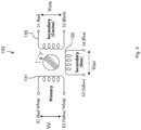
- FIG. 2 which shows a primary winding 131 of the resolver 103 and two secondary windings of the resolver 103, which secondary windings include a first secondary winding 133 and a second secondary winding 135.
- the primary winding 131 may be a rotor winding
- the secondary windings 133/135 may be two stator windings.
- the two secondary windings 133/135 are mechanically arranged such that their coils are shifted by a 90° angle.
- the sine wave signal V in induces a voltage at each of the secondary windings 133/135.
- the output voltages at the secondary windings 133/135 are amplitude-modulated versions of the sine wave signal V in , where the amplitude of the sine wave signal V in is modulated by the sine and cosine of the angle ⁇ of the motor shaft.
- K is the transfer ratio of the resolver 103.
- the transfer ratio K is a constant for a given resolver 103. Since the output voltage V sin of the first secondary winding 133 is amplitude-modulated by sin( ⁇ ), the first secondary winding 133 is also referred to as the sine winding of the resolver 103.
- the second secondary winding 135 is also referred to as the cosine winding of the resolver 103.
- the output voltage V sin is the output signal 104A in Figure 1
- the output voltage V cos is the output signal 104B in Figure 1 .
- the signal processing of the resolver decoder 130 processes digital samples of output voltages V sin and V cos within one period T (also referred to as a cycle) of the sine wave signal. Therefore, for the purpose of the signal processing performed by the resolver decoder 130, the angle of the motor shaft can be considered as a constant (e.g., constant within each period T), and is denoted as a constant angle 0 in the equations hereinafter to simplify the analysis.
- Figure 3 illustrates the input signal V in and the output signals V sin and V cos of the resolver 103, in an embodiment. In addition, Figure 3 further illustrates the motor shaft angle 0 that modulates the amplitude of the input signal V in .
- Three subplots at the top of Figure 3 illustrate signals V in , V sin , and V cos , respectively.
- the subplot at the bottom of Figure 3 illustrates the shaft angle ⁇ .
- the x-axes of the subplots are aligned and represent time, and the y-axis represents the value of the signals.
- the curve 301 in Figure 3 shows that the envelope of the modulated sine wave signal V sin follows the shape of the slow-changing modulating signal sin (0).
- the curve 303 in Figure 3 shows that the envelope of the modulated sine wave signal V cos follows the shape of the slow-changing modulating signal cos (0).
- the excitation voltage V in is generated by an exciting circuit 105, which may be or include a low-pass filter.
- the exciting circuit 105 accepts as input a pulse width modulated (PWM) signal generated by a PWM circuit 107.
- PWM pulse width modulated
- the PWM circuit 107 (also referred to as a PWM peripheral) is controlled by the CPU 109 and generates a sequence of PWM pulses which, after being processed (e.g., filtered) by the exciting circuit 105, turn into the sine wave signal V in .
- the output signals 104A and 104B from the resolver 103 are processed by a buffer circuit 119.
- the buffer circuit 119 performs signal conditioning functions, such as modifying/removing offsets (e.g., DC levels) of the output signals 104A and 104B, and/or voltage conversion.
- the voltages of the output signals 104A and 104B may have amplitudes between about 17 V and about 20 V.
- the buffer circuit 119 converts (e.g. scales) the amplitudes of output signals 104A and 104B to a voltage range compatible with an analog-to-digital (ADC) circuit 117, such as between about 3 V and about 5 V.
- ADC analog-to-digital
- the outputs of the buffer circuit 119 are signals 106A and 106B, which may be scaled versions of the signals 104A and 104B, respectively.
- the signal 106A is the signal 104A processed by the buffer circuit 119
- the signal 106B is the signal 104B processed by the buffer circuit 119.
- the outputs of the buffer circuit 119 are sent to a resolver decoder 130 (also referred to as a digital resolver decoder, or a resolver decoder circuit). Based on the digital samples of the signals 106A and 106B, the resolver decoder 130 generates an estimated angle ⁇ of the angle ⁇ of the motor shaft. As illustrated in Figure 1 , the resolver decoder 130 includes an analog-to-digital converter (ADC) circuit 117, a filter circuit 115, a hardware rectifier 113, and an angle calculation circuit 111. The ADC circuit 117 converts the signals 106A and 106B into digital samples.
- ADC analog-to-digital converter
- the filter circuit 115 computes a first weighted sum of the digital samples of the signal 106A over a pre-determined period of time (e.g., a duration of T/2), and computes a second weighted sum of the digital samples of the signal 106B over the predetermined period of time (e.g., a duration of T/2), where the pre-determined period of time is within the first half or within the second half of a period T of the sine wave signal sin( ⁇ c t ).
- the hardware rectifier 113 adjusts the signs of the first weighted sum and the second weighted sum, depending on whether the predetermined period of time is within the first half or the second half of the period T of the sine wave signal.
- the outputs of the hardware rectifier 113 are sent to the angle calculation circuit 111 to obtain an angle ⁇ as the estimate for the angle ⁇ of the motor shaft. More details are discussed herein after with reference to Figures 4 , 5 , 6A and 6B.
- the angle calculation circuit 111 is omitted in the resolver decoder 130, and the function of the angle calculation circuit 111 is performed by the CPU 109. In other words, instead of using a dedicated hardware (e.g., the angle calculation circuit 111) to compute the estimated angle ⁇ , the CPU 109 computes the estimated angle ⁇ .
- a dedicated hardware e.g., the angle calculation circuit 111
- the resolver decoder 130, the CPU 109, the memory module 108, the PWM circuit 107 (if formed), and other peripheral modules of the CPU 109 are integrated onto a same semiconductor substrate as a single semiconductor device 150, which may be referred to as a processor 150, a micro-controller 150 with integrated resolver decoder, or simply a micro-controller 150.
- a processor 150 e.g., a central processing unit (CPU)
- the disclosed micro-controller 150 has the advantage of higher integration density (thus lower cost) for the motor control system 100.
- FIG. 4 illustrates a block diagram of a resolver decoder 130, in an embodiment.
- the resolver decoder 130 of Figure 4 shows more details than that of Figure 1 , and may be used as the resolver decoder 130 of Figure 1 .
- the signals 106A and 106B are sent to the ADC circuit 117 for conversion into digital samples.
- the ADC circuit 117 may include two analog-to-digital converters 118A and 118B, or two input channels 118A and 118B, for converting the signals 106A and 106B synchronously.
- a same sampling clock signal 120 may be used to drive the circuits (e.g., 118A and 118B) for converting the signals 106A and 106B, such that the signals 106A and 106B are sampled at the same time instants. Therefore, pairs of digital samples of the signals 106A and 106B are sent to the filter circuit 115, where the two digital samples in each pair are sampled at the same time instant.
- the filter circuit 115 has two finite impulse response (FIR) filters 115A and 115B.
- FIR finite impulse response
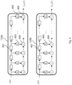
- the FIR filter 115A has a tapped-delay line (TDL) with a plurality of delay elements 401, which TDL may be implemented a plurality of serially concatenated memory elements such as flip-flops.
- the input to the TDL of the FIR filter 115A is x(n), which are the digital samples of the signal 106A.
- each coefficient 403 represents a multiplier with a corresponding scaling factor a k .
- the FIR filter 115A further has a plurality of adders 405, which sums up all the scaled values to generate the output of the FIR filter 115A. Therefore, the FIR filter 115A calculates a weighted sum of the digital samples that are at the input of the TDL and in the delay elements 401.
- the FIR filter 115B has an identical structure as the FIR filter 115A, but is used to process input data y ( n ), which are the digital samples of the signal 106B.
- the ratio between f s and f c is chosen to be 2N, where N is a positive integer (e.g., N ⁇ 10), such as 10, 20, or 100. This means that for each period T of the sine wave signal sin( ⁇ c t ), 2N digital samples are generated for the signal 106A, and 2N digital samples are generated for the signal 106B.
- the number of taps of the FIR filters 115A/115B which is m + 1, is chosen such that the duration of time covered by the TDL of each FIR filter is equal to or smaller than half of the period T, or equivalently, m ⁇ N.
- the output of the FIR filter 115A (or 115B) is the sum of digital samples disposed within the first half of the period T of the sine wave signal.
- the digital samples stored in the tapped delay line of the FIR filter 115A (or 115B) covers exactly the first half of the period T of the sine wave signal.
- Equations (5) and (6) (and (7) and (8)) omitted a positive constant scale factor, which is determined by, e.g., the positive values A and K in Equations (1) and (2), and the positive scaling factor of the buffer circuit 119.
- a positive constant scale factor in the integration values in Equations (5) and (6), or (7) and (8) does not change the result of the angle calculation performed later.
- the time delay introduced by the resolver 103, the buffer circuit 119, and the ADC circuit 117 is a fixed value, and is either known or can be measured, e.g., by a calibration process. Therefore, the timing information of the digital samples (also referred to as data samples) fed into the FIR filters 115A/115B, such as which digital sample corresponds to the starting point, the mid-point, or the end-point within a period T of the amplitude-modulated sine wave signal, is known to the CPU 109 (or the PWM circuit 107).
- the digital samples x ( n ) and y(n) at the input of the FIR filters 115A/115B that correspond to the starting point of a period T of the amplitude-modulated sine wave signal can be identified by counting a predetermined number of clock cycles (which correspond to a pre-determined time delay) from the known starting point of the sine wave signal at the output of the exciting circuit 105.
- Figure 1 shows a control signal path 123 from the PWM circuit 107 to the hardware rectifier 113.
- the control signal path 123 is used to send the timing information of the data samples, such as a pulse to indicate that the current data sample x ( n ) and y(n) at the input of the FIR filters 115A/115B are the samples corresponding to the mid-point of a period T, or equivalently, corresponding to an angle ⁇ within a period of 2 ⁇ of the sine wave signal.
- the timing formation such as the pulse discussed above, is used to indicate that the current outputs of the FIR filters 115A/115B correspond to the integration values between angles 0 and ⁇ (e.g., Equations (5) and (6)), or the integration values between angles ⁇ and 2 ⁇ (e.g., Equations (7) and (8)).
- Figure 1 shows that the timing information is sent from the PWM circuit 107 to the hardware rectifier 113, the timing information may alternatively be send from the CPU 109 to the hardware rectifier 113.
- the integration values V sin and V cos in Equations (5) and (6) provide scaled versions of sin (0) and cos (0), respectively, scaled by ⁇ 0 ⁇ sin ⁇ c d ⁇ c , which has a positive value because sin ( ⁇ c ) has positive values for angles between 0 and ⁇ .
- the integration values V sin and V cos in Equations (7) and (8) provide scaled versions of sin (0) and cos (0), respectively, scaled by ⁇ ⁇ 2 ⁇ sin ⁇ c d ⁇ c , which has a negative value because sin ( ⁇ c ) has negative values for angles between ⁇ and 2 ⁇ .
- the negative scale factor in the integration values of Equations (7) and (8) may cause error in the calculation of the estimated shaft angle ⁇ based on sin ( ⁇ ) and cos( ⁇ ). Therefore, the integration values of Equations (7) and (8) are adjusted (e.g., corrected) by multiplying with a value of -1, or equivalently, by changing (or reversing) the signs of the integration values of Equations (7) and (8), in some embodiments.
- the hardware rectifier 113 corrects the outputs of the FIR filters 115A/115B by, e.g., multiplying with a value of -1 using the multipliers 601 (e.g., 601A and 601B), when the outputs of the FIR filters 115A/115B correspond to integration values of Equations (7) and (8), or equivalently, when the data samples stored in the tapped delay lines of the FIR filters 115A/115B are data samples in the second half of a period T (e.g., between angles ⁇ and 2 ⁇ ) of the amplitude-modulated sine wave signal.
- T e.g., between angles ⁇ and 2 ⁇
- the hardware rectifier 113 passes through the outputs of the FIR filters 115A/115B, e.g., by multiplying with a value of 1.
- the sign table 603 of the hardware rectifier 113 keeps track of the signs of the outputs of the FIR filters 115/117. In other words, the sign table 603 determines whether a multiplication value of 1 or -1 is used to multiply with the outputs of the FIR filters 115A/115B. As discussed above, the control signal path 123 sends timing information of the data samples, or equivalently, timing information regarding whether the outputs of the FIR filters 115A/115B correspond to Equations (5) and (6), or Equations (7) and (8).
- control signal path 123 may send a so-called "zero-crossing pulse" once every half of the period T, which zero-crossing pulse indicates whether the current outputs of the FIR filters 115A/115B correspond to Equations (5) and (6), or Equations (7) and (8).
- the sign table 603 starts with a multiplication value of 1, and toggles the multiplication value between 1 and -1 each time a zero-crossing pulse is received.
- the hardware rectifier 113 multiplies the outputs of the FIR filters 115A/115B with a value of 1 or -1 every half period T, such that the outputs of the hardware rectifier 113 are always the values of sin (0) and cos( ⁇ ) scaled by a positive scale factor.
- the outputs of the hardware rectifier 113 are sent to the angle calculation circuit 111, which performs an arctangent function and a post processing to find an estimated angle ⁇ of the angle ⁇ .
- the arctangent function is implemented as a look-up table (LUT) as a low-cost solution, where the value of sin(0) /cos ( ⁇ ) is calculated and used as an index of the LUT to find the value of the arctangent function.
- LUT look-up table
- the angle ⁇ calculated by the arctangent function is between — ⁇ /2 and ⁇ /2
- the angle 0 of the motor shaft is between 0 and 2 ⁇ .
- a post processing is performed to calculate the estimated angle ⁇ based on the quadrant of the angle 0, which is determined by the signs of sin (0) and cos(0).
- the estimated angle ⁇ is then sent to the CPU 109.
- the CPU 109 may, based on the motor control algorithm, determine the driving voltages for the motor 101, such that the motor 101 is controlled in a closed-loop controlled fashion.
- the CPU 109 may generate a sine wave signal that lasts continuously over multiple periods of time during the operation of the motor 101.
- the above described processing, which generates an estimated angle ⁇ every half period of the sine wave signal, is performed repeatedly for each period T of the sine wave signal, so that the CPU 109 gets updated estimates of the angle ⁇ of the motor shaft twice a period of the sine wave signal.
- the disclosed FIR filters 115A/115B integrate (e.g., add) the amplitude-modulated sine wave signal over the first half or the second half of a period T of the sine wave signal, which has the advantage of improving the quality (e.g., signal-to-noise ratio (SNR)) of the calculated values for (scaled versions of) sin (0) and cos(0).
- SNR signal-to-noise ratio
- the integration operation (see Equations (5) and (6), or (7) and (8)) averages out the random noises, thereby reducing the noise power without adversely affecting the values (sin (0) and cos(0)) being calculated.
- the disclosed processing provides significantly improved accuracy in the estimated angle ⁇ .
- the coefficients of the FIR filters 115A/115B are set to a value of 1 to simplify the discussion.
- the coefficients of the FIR filters 115A/115B may be chosen to different values to improve performance. For example, digital samples corresponding to angles proximate to 0, ⁇ , and 2 ⁇ of the sine wave signal has small amplitudes, and due to the random noise in the system, these digital samples have lower quality (e.g., lower SNR) than digital samples corresponding to angles proximate to ⁇ /2 or 3 ⁇ /2.
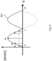
- FIG. 6 illustrates a weight assignment strategy that improves the quality of the output of the FIR filters 115A and 115B.
- the tap coefficients of the FIR filter 115A (or 115B) (see, e.g., ai, a 2 , ..., a k in Figure 6 ) are chosen to be equal to, or proportional to, the values of the sine wave signal at locations corresponding to locations of the filter taps.
- the amplitudes of the tap coefficients follow the envelope of the sine wave signal (e.g., the envelope in half of a period T).
- Figures 7A and 7B illustrate another strategy for assigning the tap coefficients of the FIR filters 115AA (or 115B).
- the tap coefficients do not follow the envelope of the sine wave signal, but are still larger for digital samples having larger amplitudes for resolver output signal, and smaller for digital samples having smaller amplitudes for resolver output signal.
- the tap coefficient may be calculated by computing the convolution of a vector A with itself, where the values in the vector A follow the envelope of the sine wave signal (e.g., in half of a period T).
- the corresponding tap coefficient B [0.019 0.073 0.169 0.308 0.478 0.660 0.828 0.951 1.000 0.951 0.828 0.660 0.478 0.308 0.169 0.073 0.019].
- Figure 7B plots the tap coefficients B. It is seen from Figure 7B that the convolution of such a vector A has a bell shape, which accentuates (e.g., amplifies) the center portion and attenuates (e.g., reduces) the tail portions (e.g., portions at the edges of the bell shape). This further improves the quality of the output of the FIR filters 115A and 115B.
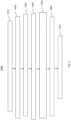
- Figure 8 illustrates another tap coefficients assignment strategy.
- only filter taps corresponding to locations around the peak of the sine wave signal are assigned non-zero values, and filter taps outside the center region (e.g., near zero-crossing locations) are assigned zero values.
- filter taps outside the center region e.g., near zero-crossing locations
- Equations (5) and (6) are over the entire first half or the entire second half of a period T of the sine wave signal
- the integration ranges, or equivalently, the spans of the tapped delay lines in the FIR filters 115A/115B do not have to cover the entire first half or the entire second half of a period T of the sine wave signal. Instead, the tapped delay lines in the FIR filters 115A/115B may only cover a portion of the first half or the second half of a period T of the sine wave signal.
- Figure 9 illustrates a flow chart of a method 1000 for operating a resolver decoder circuit, in some embodiments. It should be understood that the embodiment method shown in Figure 9 is merely an example of many possible embodiment methods. One of ordinary skill in the art would recognize many variations, alternatives, and modifications. For example, various steps as illustrated in Figure 9 may be added, removed, replaced, rearranged and repeated.
- a first analog signal is converted from a sine winding of a resolver into first data samples.
- a second analog signal is converted from a cosine winding of the resolver into second data samples.
- a first weighted sum of the first data samples is calculated over a predetermined period of time.
- a second weighted sum of the second data samples is calculated over the pre-determined period of time.
- a first sign of the first weighted sum and a second sign of the second weighted sum are adjusted based on a location of the pre-determined period of time within a cycle of a sine wave signal.
- the first weighted sum is divided by the second weighted sum to obtain a value.
- an arctangent of the value is determined to obtain an angle.
- the filter circuit 115 calculates weighted sums of the output signals from the resolver 103 to obtain scaled versions of sin (0) and cos( ⁇ ).
- the averaging effect of the filter circuit 115 reduces noise in the output of the filter circuit 115, thus improving estimates of the angle of the motor shaft.
- the filter coefficients may be assigned to follow the amplitude of the sine wave signal, thereby assigning higher weights to resolver output signals with larger amplitudes. This also improves the accuracy of the estimate of the angle of the motor shaft.
- the disclosed resolver decoder 130 provides a low-cost, hardware solution that can be integrated with the CPU 109.
- the hardware resolver decoder 130 performs computational intensive operations such as the FIR filtering, which offloads these tasks from the CPU 109 such that the real-time performance of the motor control system is improved.
Landscapes
- Engineering & Computer Science (AREA)
- Physics & Mathematics (AREA)
- General Physics & Mathematics (AREA)
- Human Computer Interaction (AREA)
- Manufacturing & Machinery (AREA)
- Automation & Control Theory (AREA)
- Theoretical Computer Science (AREA)
- Transmission And Conversion Of Sensor Element Output (AREA)
Description
- The present invention relates generally to resolver decoder and in particular, digital resolver decoder with hardware filter and hardware rectifier.
- Traction motor control is important for electrical vehicle (EV) applications. Axis rotation angle measurement plays a key role in traction motor control. The rotation angle of the motor axis (also referred to as motor shaft) is usually measured by a resolver.
- Resolvers, also known as motor resolvers, are electromagnetic transducers that can be used in a wide variety of position and velocity feedback applications, such as servo motor feedback applications. The resolver is a special type of rotary transformer that consists of a cylindrical rotor and stator. The rotor is attached to the motor shaft and rotates with the motor shaft. The resolver typically has a primary wining and two secondary windings. The primary winding may be a rotor winding on the rotor, and the secondary windings may be two stator windings on the stator. The two secondary windings are mechanically arranged such that their physical relation is shifted by a 90° angle.
- The resolver is used for generating output signals that indicate the angular position of the motor shaft, with respect to a reference point, within a space of one complete revolution of the motor shaft or within a corresponding angular displacement space from 0° to 360°. To generate the output signals, a rotor excitation signal (e.g., a sine wave signal) is applied at the primary winding. The physical relation of the secondary windings gives rise to a mathematical/electrical relation, such that a first output signal at a first one of the secondary windings is a sine wave signal amplitude-modulated by sin(0), and a second output signal at a second one of the secondary windings is a sine wave signal amplitude-modulated by cos(Ø), where 0 is the angular position of the motor shaft (may also be referred to as the
angle 0 of the motor shaft). The resolver output signals are then decoded by a resolver decoder to obtain an estimate of theangle 0. There is a need in the art for resolver decoders that provide accurate estimate of theangle 0 with lower hardware cost and/or lower computing power requirements. - Document
US 2018/205391 A1 , taken as a model for the preamble ofclaim 1, discloses a resolver to digital converter including first and second inputs to receive signals from a resolver and an output to provide an estimated angle of a rotor. The sine component signal is multiplied by the cosine of the estimated angle and the cosine component signal is multiplied by the sine of the estimated angle, and a difference between them is calculated to provide an error measurement. The estimated angle is updated by the error measurement. -
Document EP 1 471 332 A1 discloses a system with magnetic sensors that provide sine and cosine values of an angle to be determined. A pair of delta-sigma modulators performs amplification and analog-to- digital conversion of the values. A pair of decimation filters filter and down- sample bit streams. A pair of normalization stages perform processing of normalization parameters. A processor computes the angle using the output from the stages. - Document
US 2019/280537 A1 discloses a synthesis circuit that synthesizes detection signals from a plurality of detection coils to generate a synthesized detection signal indicating a sine component of a rotation angle of a rotor. The detection coils include a detection coil of a salient pole installed at a first electrical angle based on a first pole of the rotor and detection coils of salient poles installed at a second electrical angle different from the first electrical angle based on the first pole, while not including detection coils installed at the first electrical angle based on a second pole. - Document
US 2012/143 420 A1 discloses an apparatus for determining presence of an abnormality in an angle detection device configured to output an output signal having a value equivalent to a rotational angle of a rotating body. The apparatus includes a smoothing means configured to receive the output signal of the angle detection device to smooth a dependent variable of a function whose independent variable is the rotational angle equivalent value, and a parameter calculation means for calculating an abnormality determination parameter based on the dependent variable smoothed by the smoothing means. - Document
WO 02/31432 A2 - Some embodiments relate to a resolver decoder circuit according to
claim 1. - Advantageous developments thereof are recited in claims 2 to 8.
- Some embodiments relate to a processor according to claim 9, having an integrated resolver decoder circuit.
- The details of one or more embodiments of the invention are set forth in the accompanying drawings and the description below. Other features, objects, and advantages of the invention will be apparent from the description and drawings, and from the claims. In the figures, identical reference symbols generally designate the same component parts throughout the various views, which will generally not be re-described in the interest of brevity. For a more complete understanding of the invention, reference is now made to the following descriptions taken in conjunction with the accompanying drawings, in which:
-
Figure 1 illustrates a block diagram of a motor system; -
Figure 2 illustrates the primary winding and secondary windings in a resolver; -
Figure 3 illustrates the input signal and output signals of a resolver; -
Figure 4 illustrates a block diagram of a resolver decoder; -
Figure 5 illustrates a schematic view of the digital filters in a resolver decoder; -
Figure 6 illustrates a strategy for assigning filter tap coefficients; -
Figures 7A and 7B illustrate a strategy for assigning filter tap coefficients; -
Figure 8 illustrates a strategy for assigning filter tap coefficients; and -
Figure 9 illustrates a flow chart of a method for operating a resolver decoder circuit. - The making and using of the presently preferred embodiments are discussed in detail below. It should be appreciated, however, that the present invention provides many applicable inventive concepts that can be embodied in a wide variety of specific contexts. The specific embodiments discussed are merely illustrative of specific ways to make and use the invention, and do not limit the scope of the invention.
- The present invention will be described with respect to exemplary embodiments in a specific context, namely digital resolver decoder with hardware filter and hardware rectifier.
-
Figure 1 illustrates a block diagram of amotor system 100, in an embodiment. Note that for simplicity, not all features of themotor system 100 are illustrated. - Referring to
Figure 1 , themotor control system 101 includes amotor 101, which may be, e.g., a three-phase motor. Themotor 101 is driven by apower stage 121, which may include driver circuits that provide the driving voltages for themotor 101. For example, thepower stage 121 may include three parallel driver circuits, each for driving one of the three-phases of themotor 101. Each of the driver circuits may have its respective power switches (e.g., a high-side power switch and a lower-side power switch). Thepower stage 121 is controlled by a central processing unit (CPU) 109. TheCPU 109 has a memory module 108 (e.g., a non-volatile memory). Thememory module 108 may store computer programs (e.g. computer codes) for motor control algorithms. In addition, thememory module 108 may store various parameters related to, e.g., system settings, or filter coefficients for afilter circuit 115. - As illustrated in
Figure 1 , the rotor of theresolver 103 is coupled to the motor shaft, such that the rotor rotates with the motor shaft. The two secondary windings of theresolver 103 provides twooutput signals angle 0 of the motor shaft.Figures 2 and3 illustrate details regarding theresolver 103 and theoutput signals - Referring temporarily to
Figure 2 , which shows a primary winding 131 of theresolver 103 and two secondary windings of theresolver 103, which secondary windings include a first secondary winding 133 and a second secondary winding 135. The primary winding 131 may be a rotor winding, and thesecondary windings 133/135 may be two stator windings. The twosecondary windings 133/135 are mechanically arranged such that their coils are shifted by a 90° angle. - The
resolver 103 generates output signals at thesecondary windings 133/135 by energizing or exciting the primary winding 131 with an excitation voltage Vin, which is a sine wave signal represented by Vin = A * sin(ωct), where ωc is the angular frequency of the sine wave signal, and A is the amplitude of the sine wave signal. The sine wave signal Vin induces a voltage at each of thesecondary windings 133/135. The output voltages at thesecondary windings 133/135 are amplitude-modulated versions of the sine wave signal Vin, where the amplitude of the sine wave signal Vin is modulated by the sine and cosine of the angle Ø of the motor shaft. For example, a voltage Vsin across terminals of the first secondary winding 133 and a voltage Vcos across terminals of the second secondary winding 135 may be represented by

resolver 103. The transfer ratio K is a constant for a givenresolver 103. Since the output voltage Vsin of the first secondary winding 133 is amplitude-modulated by sin(Ø), the first secondary winding 133 is also referred to as the sine winding of theresolver 103. Similarly, the second secondary winding 135 is also referred to as the cosine winding of theresolver 103. In the illustrated example, the output voltage Vsin is theoutput signal 104A inFigure 1 , and the output voltage Vcos is theoutput signal 104B inFigure 1 . - Note that the
angle 0 of the motor shaft is actually a time varying signal and may be represented by 0(t) = ωmt, where ωm is the angular frequency of the motor shaft. However, the angular frequency ωc of the sine wave signal Vin is chosen to be much higher than the angular frequency ωm of the motor shaft (e.g., ωc » ωm ), and therefore, during a period T of the sine wave signal (T = 2π/ωc ), the angle of the motor shaft changes very little and can be considered as a constant. As will be discussed in more details hereinafter, the signal processing of theresolver decoder 130 processes digital samples of output voltages Vsin and Vcos within one period T (also referred to as a cycle) of the sine wave signal. Therefore, for the purpose of the signal processing performed by theresolver decoder 130, the angle of the motor shaft can be considered as a constant (e.g., constant within each period T), and is denoted as aconstant angle 0 in the equations hereinafter to simplify the analysis.Figure 3 illustrates the input signal Vin and the output signals Vsin and Vcos of theresolver 103, in an embodiment. In addition,Figure 3 further illustrates themotor shaft angle 0 that modulates the amplitude of the input signal Vin. Three subplots at the top ofFigure 3 illustrate signals Vin, Vsin, and Vcos, respectively. The subplot at the bottom ofFigure 3 illustrates the shaft angle Ø. The x-axes of the subplots are aligned and represent time, and the y-axis represents the value of the signals. Thecurve 301 inFigure 3 shows that the envelope of the modulated sine wave signal Vsin follows the shape of the slow-changing modulating signal sin (0). Similarly, thecurve 303 inFigure 3 shows that the envelope of the modulated sine wave signal Vcos follows the shape of the slow-changing modulating signal cos (0). Referring back toFigure 1 , the excitation voltage Vin is generated by anexciting circuit 105, which may be or include a low-pass filter. Theexciting circuit 105 accepts as input a pulse width modulated (PWM) signal generated by aPWM circuit 107. The PWM circuit 107 (also referred to as a PWM peripheral) is controlled by theCPU 109 and generates a sequence of PWM pulses which, after being processed (e.g., filtered) by theexciting circuit 105, turn into the sine wave signal Vin. - Still referring to
Figure 1 , theoutput signals resolver 103 are processed by abuffer circuit 119. Thebuffer circuit 119 performs signal conditioning functions, such as modifying/removing offsets (e.g., DC levels) of theoutput signals output signals buffer circuit 119 converts (e.g. scales) the amplitudes ofoutput signals circuit 117, such as between about 3 V and about 5 V. The outputs of thebuffer circuit 119 aresignals signals signal 106A is thesignal 104A processed by thebuffer circuit 119, and thesignal 106B is thesignal 104B processed by thebuffer circuit 119. - The outputs of the
buffer circuit 119 are sent to a resolver decoder 130 (also referred to as a digital resolver decoder, or a resolver decoder circuit). Based on the digital samples of thesignals resolver decoder 130 generates an estimated angle Ø̃ of the angle Ø of the motor shaft. As illustrated inFigure 1 , theresolver decoder 130 includes an analog-to-digital converter (ADC)circuit 117, afilter circuit 115, ahardware rectifier 113, and anangle calculation circuit 111. TheADC circuit 117 converts thesignals filter circuit 115 computes a first weighted sum of the digital samples of thesignal 106A over a pre-determined period of time (e.g., a duration of T/2), and computes a second weighted sum of the digital samples of thesignal 106B over the predetermined period of time (e.g., a duration of T/2), where the pre-determined period of time is within the first half or within the second half of a period T of the sine wave signal sin(ωct). Thehardware rectifier 113 adjusts the signs of the first weighted sum and the second weighted sum, depending on whether the predetermined period of time is within the first half or the second half of the period T of the sine wave signal. The outputs of thehardware rectifier 113 are sent to theangle calculation circuit 111 to obtain an angle Ø̃ as the estimate for the angle Ø of the motor shaft. More details are discussed herein after with reference toFigures 4 ,5 , 6A and 6B. - In some embodiments, the
angle calculation circuit 111 is omitted in theresolver decoder 130, and the function of theangle calculation circuit 111 is performed by theCPU 109. In other words, instead of using a dedicated hardware (e.g., the angle calculation circuit 111) to compute the estimated angle Ø̃, theCPU 109 computes the estimated angle Ø̃. - In some embodiments, the
resolver decoder 130, theCPU 109, thememory module 108, the PWM circuit 107 (if formed), and other peripheral modules of theCPU 109 are integrated onto a same semiconductor substrate as asingle semiconductor device 150, which may be referred to as aprocessor 150, amicro-controller 150 with integrated resolver decoder, or simply amicro-controller 150. Compared with a solution where theresolver decoder 130 is implemented in a dedicated semiconductor device (e.g., an application-specific integrated circuit (ASIC)) and theCPU 109 is implemented in another device, the disclosedmicro-controller 150 has the advantage of higher integration density (thus lower cost) for themotor control system 100. Compared with a software solution whereCPU 109 implements some or all of the functions of theresolver decoder 130, the disclosed structure of the micro-controller 150 offloads computation intensive tasks (e.g., the tasks of computing the output of the filter circuit 115) to hardware circuits, so theCPU 109 can have more computational resources reserved for other system tasks. As a result, the real-time performance of themotor control system 100 is improved.Figure 4 illustrates a block diagram of aresolver decoder 130, in an embodiment. Theresolver decoder 130 ofFigure 4 shows more details than that ofFigure 1 , and may be used as theresolver decoder 130 ofFigure 1 . - As illustrated in
Figure 4 , thesignals 106A (e.g., corresponding to the Vsin signal) and 106B (e.g., corresponding to the Vcos signal) are sent to theADC circuit 117 for conversion into digital samples. TheADC circuit 117 may include two analog-to-digital converters input channels signals sampling clock signal 120 may be used to drive the circuits (e.g., 118A and 118B) for converting thesignals signals signals filter circuit 115, where the two digital samples in each pair are sampled at the same time instant. - The
filter circuit 115 has two finite impulse response (FIR) filters 115A and 115B. - The digital samples of the
signal 106A are sent to theFIR filter 115A, and the digital samples of thesignal 106B are sent to theFIR filter 115B. Details of the FIR filters 115A and 115B are illustrated inFigure 5 . - Referring temporarily to
Figure 5 , which shows the schematic view of the FIR filters 115A and 115B. As illustrated inFigure 5 , theFIR filter 115A has a tapped-delay line (TDL) with a plurality ofdelay elements 401, which TDL may be implemented a plurality of serially concatenated memory elements such as flip-flops. The input to the TDL of theFIR filter 115A is x(n), which are the digital samples of thesignal 106A. The TDL has a plurality of taps, and each of the taps has a respective coefficient 403 (labeled as ak, k=0, 1, 2, ..., m), which coefficient is used to scale (e.g., multiply with) the values at the tap. In other words, each coefficient 403 represents a multiplier with a corresponding scaling factor ak. TheFIR filter 115A further has a plurality ofadders 405, which sums up all the scaled values to generate the output of theFIR filter 115A. Therefore, theFIR filter 115A calculates a weighted sum of the digital samples that are at the input of the TDL and in thedelay elements 401. TheFIR filter 115B has an identical structure as theFIR filter 115A, but is used to process input data y(n), which are the digital samples of thesignal 106B. In addition, thefilter coefficients 403 of theFIR filter 115B are denoted as bk, k=0, 1, 2, ...m, which may be chosen independently from the coefficients ak of theFIR filter 115A. The output of the FIR filters 115A and 115B are given by:

- In the illustrated embodiment, the sampling frequency fs of the
ADC circuit 117 is chosen to be orders of magnitude higher (e.g., 10 times, 20 times, 100 times, or more) than that frequency fc of the sine wave signal sin(ωct), where fc = ωc /(2π). In an example embodiment, the ratio between fs and fc is chosen to be 2N, where N is a positive integer (e.g., N≥10), such as 10, 20, or 100. This means that for each period T of the sine wave signal sin(ωct), 2N digital samples are generated for thesignal 106A, and 2N digital samples are generated for thesignal 106B. In addition, the number of taps of the FIR filters 115A/115B, which is m + 1, is chosen such that the duration of time covered by the TDL of each FIR filter is equal to or smaller than half of the period T, or equivalently, m≤N. - In some embodiments, the filter coefficients ak and bk are chosen to be 1, such that the FIR filters 115A and 115B simply calculate the sum of all the digital samples within a duration of mTs, where Ts = 1/fs is the sampling period of the
ADC circuit 117. When the oldest digital sample in the TDL (e.g., the digital sample stored in therightmost delay element 401 of the TDL) of theFIR filter 115A (or 115B) corresponds to a sample of thesignal 106A (or 106B) at the starting point (e.g., t = 0) of a period T of the sine wave signal sin(ωct), the output of theFIR filter 115A (or 115B) is the sum of digital samples disposed within the first half of the period T of the sine wave signal. In particular, where m=N, the digital samples stored in the tapped delay line of theFIR filter 115A (or 115B) covers exactly the first half of the period T of the sine wave signal. With the sampling frequency fs being much higher than the frequency fc of the sine wave signal sin(ωct), the outputs of the FIR filters 115A and 115B in Equation (3) and (4) provide close approximations to the following integration values respectively:

- For similar reasons, when the oldest digital sample stored in the tapped delay line of the
FIR filter 115A (or 115B) corresponds to a sample of thesignal 106A (or 106B) at mid-point of the period T (e.g., t = T/2) of the sine wave signal sin(ωct), the outputs of thefilters 

- Note that for simplicity, the integration values in Equations (5) and (6) (and (7) and (8)) omitted a positive constant scale factor, which is determined by, e.g., the positive values A and K in Equations (1) and (2), and the positive scaling factor of the
buffer circuit 119. As will be discussed hereinafter, a positive constant scale factor in the integration values in Equations (5) and (6), or (7) and (8), does not change the result of the angle calculation performed later. - Recall that in
Figure 1 , the PWM pulses, which is used by theexciting circuit 105 to generate the sine wave signal sin(ωct), is generated under the control of theCPU 109. Therefore, the timing of the sine wave signal sin(ωct), such as the starting point (e.g., t = 0), the mid-point (e.g., t = T/2), or the end-point (e.g., t = T) of a period T of the sine wave signal sin(ωct), is known to theCPU 109. In addition, the time delay introduced by theresolver 103, thebuffer circuit 119, and theADC circuit 117 is a fixed value, and is either known or can be measured, e.g., by a calibration process. Therefore, the timing information of the digital samples (also referred to as data samples) fed into the FIR filters 115A/115B, such as which digital sample corresponds to the starting point, the mid-point, or the end-point within a period T of the amplitude-modulated sine wave signal, is known to the CPU 109 (or the PWM circuit 107). For example, the digital samples x(n) and y(n) at the input of the FIR filters 115A/115B that correspond to the starting point of a period T of the amplitude-modulated sine wave signal can be identified by counting a predetermined number of clock cycles (which correspond to a pre-determined time delay) from the known starting point of the sine wave signal at the output of theexciting circuit 105. -
Figure 1 shows acontrol signal path 123 from thePWM circuit 107 to thehardware rectifier 113. In some embodiments, thecontrol signal path 123 is used to send the timing information of the data samples, such as a pulse to indicate that the current data sample x(n) and y(n) at the input of the FIR filters 115A/115B are the samples corresponding to the mid-point of a period T, or equivalently, corresponding to an angle π within a period of 2π of the sine wave signal. The timing formation, such as the pulse discussed above, is used to indicate that the current outputs of the FIR filters 115A/115B correspond to the integration values betweenangles 0 and π (e.g., Equations (5) and (6)), or the integration values between angles π and 2π (e.g., Equations (7) and (8)). AlthoughFigure 1 shows that the timing information is sent from thePWM circuit 107 to thehardware rectifier 113, the timing information may alternatively be send from theCPU 109 to thehardware rectifier 113. - Note that the integration values Vsin and Vcos in Equations (5) and (6) provide scaled versions of sin (0) and cos (0), respectively, scaled by


- Referring back to
Figure 4 , thehardware rectifier 113 corrects the outputs of the FIR filters 115A/115B by, e.g., multiplying with a value of -1 using the multipliers 601 (e.g., 601A and 601B), when the outputs of the FIR filters 115A/115B correspond to integration values of Equations (7) and (8), or equivalently, when the data samples stored in the tapped delay lines of the FIR filters 115A/115B are data samples in the second half of a period T (e.g., between angles π and 2π) of the amplitude-modulated sine wave signal. Conversely, when the outputs of the FIR filters 115A/115B correspond to integration values of Equations (5) and (6), or equivalently, when the data samples stored in the tapped delay lines of the FIR filters 115A/115B are data samples in the first half of a period T (e.g., betweenangles 0 and π) of the amplitude-modulated sine wave signal, thehardware rectifier 113 passes through the outputs of the FIR filters 115A/115B, e.g., by multiplying with a value of 1. - The sign table 603 of the
hardware rectifier 113 keeps track of the signs of the outputs of the FIR filters 115/117. In other words, the sign table 603 determines whether a multiplication value of 1 or -1 is used to multiply with the outputs of the FIR filters 115A/115B. As discussed above, thecontrol signal path 123 sends timing information of the data samples, or equivalently, timing information regarding whether the outputs of the FIR filters 115A/115B correspond to Equations (5) and (6), or Equations (7) and (8). For example, thecontrol signal path 123 may send a so-called "zero-crossing pulse" once every half of the period T, which zero-crossing pulse indicates whether the current outputs of the FIR filters 115A/115B correspond to Equations (5) and (6), or Equations (7) and (8). In some embodiments, the sign table 603 starts with a multiplication value of 1, and toggles the multiplication value between 1 and -1 each time a zero-crossing pulse is received. Therefore, in the illustrated embodiment, thehardware rectifier 113 multiplies the outputs of the FIR filters 115A/115B with a value of 1 or -1 every half period T, such that the outputs of thehardware rectifier 113 are always the values of sin (0) and cos(Ø) scaled by a positive scale factor. - Still referring to
Figure 4 , the outputs of thehardware rectifier 113 are sent to theangle calculation circuit 111, which performs an arctangent function and a post processing to find an estimated angle Ø̃ of the angle Ø. In particular, theangle calculation circuit 111 finds a first angle α by
- In some embodiments, the arctangent function is implemented as a look-up table (LUT) as a low-cost solution, where the value of sin(0) /cos (Ø) is calculated and used as an index of the LUT to find the value of the arctangent function. Note that the angle α calculated by the arctangent function is between —π/2 and π/2, whereas the
angle 0 of the motor shaft is between 0 and 2π. A post processing is performed to calculate the estimated angle Ø̃ based on the quadrant of theangle 0, which is determined by the signs of sin (0) and cos(0). For example, if, based on the signs of sin (0) and cos(Ø), the angle Ø is in the first quadrant, then Ø̃ = α; if the angle Ø is in the second quadrant, then Ø̃ = π - α; if the angle Ø is in the third quadrant, then Ø̃ = π + α; and if the angle Ø is in the fourth quadrant, then Ø̃ = 2π - α. The estimated angle Ø̃ is then sent to theCPU 109. TheCPU 109 may, based on the motor control algorithm, determine the driving voltages for themotor 101, such that themotor 101 is controlled in a closed-loop controlled fashion. One skilled in the art will readily appreciate that theCPU 109 may generate a sine wave signal that lasts continuously over multiple periods of time during the operation of themotor 101. The above described processing, which generates an estimated angle Ø̃ every half period of the sine wave signal, is performed repeatedly for each period T of the sine wave signal, so that theCPU 109 gets updated estimates of the angle Ø of the motor shaft twice a period of the sine wave signal. The disclosedFIR filters 115A/115B integrate (e.g., add) the amplitude-modulated sine wave signal over the first half or the second half of a period T of the sine wave signal, which has the advantage of improving the quality (e.g., signal-to-noise ratio (SNR)) of the calculated values for (scaled versions of) sin (0) and cos(0). This is because in real systems, the output voltage Vsin and Vcos of theresolver 103 has noises (e.g., random noises), which degrade the quality of the output voltages. The integration operation (see Equations (5) and (6), or (7) and (8)) averages out the random noises, thereby reducing the noise power without adversely affecting the values (sin (0) and cos(0)) being calculated. Compared with a method where each pair of digital samples from theADC circuit 117 are used directly to compute the arctangent, the disclosed processing provides significantly improved accuracy in the estimated angle Ø̃. - In the discussion above, the coefficients of the FIR filters 115A/115B are set to a value of 1 to simplify the discussion. The coefficients of the FIR filters 115A/115B, however, may be chosen to different values to improve performance. For example, digital samples corresponding to angles proximate to 0, π, and 2π of the sine wave signal has small amplitudes, and due to the random noise in the system, these digital samples have lower quality (e.g., lower SNR) than digital samples corresponding to angles proximate to π/2 or 3π/2. Therefore, it may be advantageous to assign smaller weights (e.g., filter coefficients with smaller values) for the digital samples with lower quality (e.g., near zero-crossing locations of the sine wave signal), and to assign higher weights for the digital samples with higher quality (e.g., near maximum value locations of the sine wave signal).
Figure 6 illustrates a weight assignment strategy that improves the quality of the output of the FIR filters 115A and 115B. - Referring to
Figure 6 , the tap coefficients of theFIR filter 115A (or 115B) (see, e.g., ai, a2, ..., ak inFigure 6 ) are chosen to be equal to, or proportional to, the values of the sine wave signal at locations corresponding to locations of the filter taps. For example, the amplitudes of the tap coefficients follow the envelope of the sine wave signal (e.g., the envelope in half of a period T). -
Figures 7A and 7B illustrate another strategy for assigning the tap coefficients of the FIR filters 115AA (or 115B). In the example ofFigures 7A and 7B , the tap coefficients do not follow the envelope of the sine wave signal, but are still larger for digital samples having larger amplitudes for resolver output signal, and smaller for digital samples having smaller amplitudes for resolver output signal. For example, the tap coefficient may be calculated by computing the convolution of a vector A with itself, where the values in the vector A follow the envelope of the sine wave signal (e.g., in half of a period T).Figure 7A plots an example vector A=[0.309 0.588 0.809 0.951 1.000 0.951 0.809 0.588 0.309]. The tap coefficient, denoted by a vector B, is the convolution of the vector A with itself (e.g., B = A * A). For the above example vector A, the corresponding tap coefficient B=[0.019 0.073 0.169 0.308 0.478 0.660 0.828 0.951 1.000 0.951 0.828 0.660 0.478 0.308 0.169 0.073 0.019].Figure 7B plots the tap coefficients B. It is seen fromFigure 7B that the convolution of such a vector A has a bell shape, which accentuates (e.g., amplifies) the center portion and attenuates (e.g., reduces) the tail portions (e.g., portions at the edges of the bell shape). This further improves the quality of the output of the FIR filters 115A and 115B. -
Figure 8 illustrates another tap coefficients assignment strategy. InFigure 8 , only filter taps corresponding to locations around the peak of the sine wave signal (see the center region Δα around the peak of the sine wave signal inFigure 8 ) are assigned non-zero values, and filter taps outside the center region (e.g., near zero-crossing locations) are assigned zero values. In other words, only digital samples with high SNRs are used in calculation. - While the integrations in Equations (5) and (6) (or (7) and (8)) are over the entire first half or the entire second half of a period T of the sine wave signal, one skilled in the art will readily appreciate that these are merely non-limiting examples. The integration ranges, or equivalently, the spans of the tapped delay lines in the FIR filters 115A/115B, do not have to cover the entire first half or the entire second half of a period T of the sine wave signal. Instead, the tapped delay lines in the FIR filters 115A/115B may only cover a portion of the first half or the second half of a period T of the sine wave signal.
-
Figure 9 illustrates a flow chart of amethod 1000 for operating a resolver decoder circuit, in some embodiments. It should be understood that the embodiment method shown inFigure 9 is merely an example of many possible embodiment methods. One of ordinary skill in the art would recognize many variations, alternatives, and modifications. For example, various steps as illustrated inFigure 9 may be added, removed, replaced, rearranged and repeated. - Referring to
Figure 9 , atblock 1010, a first analog signal is converted from a sine winding of a resolver into first data samples. Atblock 1020, a second analog signal is converted from a cosine winding of the resolver into second data samples. Atblock 1030, a first weighted sum of the first data samples is calculated over a predetermined period of time. Atblock 1040, a second weighted sum of the second data samples is calculated over the pre-determined period of time. Atblock 1050, a first sign of the first weighted sum and a second sign of the second weighted sum are adjusted based on a location of the pre-determined period of time within a cycle of a sine wave signal. Atblock 1060, after the adjusting, the first weighted sum is divided by the second weighted sum to obtain a value. Atblock 1070, an arctangent of the value is determined to obtain an angle. - Disclosed embodiments may achieve advantages. For example, the
filter circuit 115 calculates weighted sums of the output signals from theresolver 103 to obtain scaled versions of sin (0) and cos(Ø). The averaging effect of thefilter circuit 115 reduces noise in the output of thefilter circuit 115, thus improving estimates of the angle of the motor shaft. In addition, the filter coefficients may be assigned to follow the amplitude of the sine wave signal, thereby assigning higher weights to resolver output signals with larger amplitudes. This also improves the accuracy of the estimate of the angle of the motor shaft. By performing the integration operation over a duration within half of a period T of the sine wave signal, the sign of the output of the integration operation can be easily adjusted by thehardware rectifier 113. Compared with an integration over the full period T where each of the data samples in the second half of the period T needs to be multiplied with -1, the disclosed structure allows a lowcomplexity hardware rectifier 113 to be used. The disclosedresolver decoder 130 provides a low-cost, hardware solution that can be integrated with theCPU 109. Thehardware resolver decoder 130 performs computational intensive operations such as the FIR filtering, which offloads these tasks from theCPU 109 such that the real-time performance of the motor control system is improved.
Claims (9)
- A resolver decoder circuit (130) comprising:a first filter circuit (115A) configured to calculate a first weighted sum of a first digital signal over a pre-determined period of time, wherein the first digital signal comprises first digital samples of a first analog signal (106A) from a first secondary winding (133) of a resolver (103);a second filter circuit (115B) configured to calculate a second weighted sum of a second digital signal over the pre-determined period of time, wherein the second digital signal comprises second digital samples of a second analog signal (106B) from a second secondary winding (135) of the resolver (103), wherein the first analog signal (106A) and the second analog signal (106B) are configured to be induced by a sine wave signal applied to an input winding (131) of the resolver (103); anda rectifier (113) configured to generate a first output and a second output by adjusting (603) a first sign of the first weighted sum and adjusting a second sign of the second weighted sum, respectively,the circuit characterized in that each of the first filter circuit (115A) and the second filter circuit (115B) comprises:an input terminal;an output terminal;a tapped delay line, TDL (401) coupled to the input terminal and having taps, wherein each of the taps of the TDL has a respective weight factor (403); anda plurality of adders (405) configured to generate, at the output terminal, a weighted sum of digital values at the taps of the TDL (401).
- The resolver decoder circuit (130) of claim 1, wherein the rectifier (113) has an input terminal configured to receive a control signal (123) that indicates whether the pre-determined period of time corresponds to a first half of a period of the sine wave signal or a second half of a period of the sine wave signal.
- The resolver decoder circuit (130) of claim 2, wherein the rectifier (113) is configured to:reversing the first sign of the first weighted sum and the second sign of the second weighted sum when the control signal (123) indicates that the predetermined period of time corresponds to the second half of a period of the sine wave signal; andkeeping the first sign of the first weighted sum and the second sign of the second weighted sum unchanged when the pre-determined period of time corresponds to the first half of a period of the sine wave signal.
- The resolver decoder circuit (130) of claim 1, further comprising an analog-to-digital converter, ADC circuit (117), wherein the ADC circuit (117) is configured to sample the first analog signal (106A) and the second analog signal (106B) using a same sampling clock signal (120).
- The resolver decoder circuit (130) of claim 1, further comprising an angle calculation circuit (111), wherein the angle calculation circuit (111) is configured to:calculate (111) a ratio between the first output of the rectifier (113) and the second output of the rectifier (113); anddetermine a first angle by performing an arctangent function on the ratio.
- The resolver decoder circuit (130) of claim 5:wherein the first secondary winding (133) of the resolver (103) is a sine winding, and the second secondary winding (135) of the resolver (103) is a cosine winding, and/orwherein the angle calculation circuit (111) is further configured to:determine, based on signs of the first output and the second output of the rectifier (113), a quadrant of an angle indicated by the first analog signal (106A) and the second analog signal (106B); anddetermine the angle indicated by the first analog signal (106A) and the second analog signal (106B) by adjusting the first angle based on the determined quadrant.
- The resolver decoder circuit (130) of claim 1, wherein the weight factors (403) of the TDL are equal.
- The resolver decoder circuit (130) of claim 1, wherein the weight factors (403) of the TDL are different, and wherein amplitudes of the weight factors (403) of the TDL preferably follow an envelope of the sine wave signal.
- A processor (150) having integrated therein a resolver decoder circuit (103) according to claim 1, wherein the processor (150) comprises:an analog-to-digital converter, ADC circuit (117) configured to:generate said first digital samples by converting a first analog signal (106A) from a sine winding (133) of a resolver (103), andgenerate said second digital samples by converting a second analog signal (106B) from a cosine winding (135) of the resolver (103), the first analog signal (106A) and the second analog signal (106B) being generated by exciting an input winding (131) of the resolver (103) with a sine wave signal;a first tapped delay line, TDL filter (115A) coupled to the ADC circuit (117) and configured to calculate said first weighted sum of the first digital samples over a pre-determined period of time;a second TDL filter (115B) coupled to the ADC circuit (117) and configured to calculate said second weighted sum of the second digital samples over the predetermined period of time;said rectifier (113) configured to generate a first output and a second output by adjusting a first sign of the first weighted sum and a second sign of the second weighted sum, respectively; anda central processing unit, CPU (109) coupled to the rectifier (113).
Applications Claiming Priority (1)
| Application Number | Priority Date | Filing Date | Title |
|---|---|---|---|
| US17/360,702 US11567471B2 (en) | 2021-06-28 | 2021-06-28 | Digital resolver decoder with hardware filter and rectifier |
Publications (2)
| Publication Number | Publication Date |
|---|---|
| EP4113070A1 EP4113070A1 (en) | 2023-01-04 |
| EP4113070B1 true EP4113070B1 (en) | 2025-01-01 |
Family
ID=82214407
Family Applications (1)
| Application Number | Title | Priority Date | Filing Date |
|---|---|---|---|
| EP22180325.7A Active EP4113070B1 (en) | 2021-06-28 | 2022-06-22 | Digital resolver decoder with hardware filter and rectifier |
Country Status (3)
| Country | Link |
|---|---|
| US (1) | US11567471B2 (en) |
| EP (1) | EP4113070B1 (en) |
| CN (1) | CN115603754A (en) |
Families Citing this family (3)
| Publication number | Priority date | Publication date | Assignee | Title |
|---|---|---|---|---|
| CN120101838A (en) * | 2023-11-30 | 2025-06-06 | 芯海科技(深圳)股份有限公司 | Resolver processing circuit, method, chip and electronic device |
| US12597945B2 (en) * | 2024-04-25 | 2026-04-07 | Infineon Technologies Ag | Machine learning enhanced resolver systems |
| CN119420363B (en) * | 2025-01-09 | 2025-04-15 | 峰岹科技(深圳)股份有限公司 | Demodulation device, rotational digital converter and storage medium |
Family Cites Families (15)
| Publication number | Priority date | Publication date | Assignee | Title |
|---|---|---|---|---|
| IL138983A0 (en) | 2000-10-12 | 2001-11-25 | Netzer Prec Motion Sensors Ltd | Capacitive displacement encoder |
| US6754610B2 (en) | 2001-05-16 | 2004-06-22 | Raytheon Company | Digital signal processing of resolver rotor angle signals |
| JP2004279231A (en) | 2003-03-17 | 2004-10-07 | Minebea Co Ltd | R/d converter |
| EP1471332A1 (en) | 2003-04-17 | 2004-10-27 | Dialog Semiconductor GmbH | Digital interface for an angular sensor |
| US7508154B1 (en) * | 2006-05-15 | 2009-03-24 | Quicksilver Controls, Inc. | Integrated motor and resolver including absolute position capability |
| CN101521480B (en) * | 2008-11-21 | 2010-10-13 | 西北工业大学 | A resolver signal resolution method and resolver |
| CN101567658B (en) * | 2009-06-05 | 2010-12-01 | 中国兵器工业第二○六研究所 | Rotating transformer exciting circuit based on sinusoidal pulse width modulation (SPWM) |
| JP5333583B2 (en) | 2010-11-08 | 2013-11-06 | トヨタ自動車株式会社 | Rotation angle calculation device and rotation angle calculation method |
| JP5895442B2 (en) | 2010-12-01 | 2016-03-30 | 株式会社デンソー | Abnormality judgment device for angle detection device |
| CN102661754B (en) * | 2012-05-09 | 2014-06-25 | 合肥工业大学 | Resolver to Digital Converter |
| RU2541856C2 (en) * | 2013-06-28 | 2015-02-20 | Открытое Акционерное общество "Ростовский оптико-механический завод" | Digital angle converter |
| CN103475374A (en) * | 2013-08-09 | 2013-12-25 | 浙江吉利汽车研究院有限公司 | Rotary transformer decoding deck and decoding method thereof |
| US9528857B2 (en) | 2014-10-17 | 2016-12-27 | Infineon Technologies Ag | Time capture based resolver to digital converter |
| US10027344B1 (en) | 2017-01-18 | 2018-07-17 | Raytheon Company | Resolver to digital conversion apparatus and method |
| JP7067968B2 (en) | 2018-03-12 | 2022-05-16 | ルネサスエレクトロニクス株式会社 | Rotation angle sensor system and semiconductor device |
-
2021
- 2021-06-28 US US17/360,702 patent/US11567471B2/en active Active
-
2022
- 2022-06-22 EP EP22180325.7A patent/EP4113070B1/en active Active
- 2022-06-27 CN CN202210742340.6A patent/CN115603754A/en active Pending
Also Published As
| Publication number | Publication date |
|---|---|
| EP4113070A1 (en) | 2023-01-04 |
| US20220413462A1 (en) | 2022-12-29 |
| US11567471B2 (en) | 2023-01-31 |
| CN115603754A (en) | 2023-01-13 |
Similar Documents
| Publication | Publication Date | Title |
|---|---|---|
| EP4113070A1 (en) | Digital resolver decoder with hardware filter and rectifier | |
| US6084376A (en) | Low cost resolver system | |
| US7895010B2 (en) | Resolver angle detection device and method of detecting position with a resolver | |
| US6754610B2 (en) | Digital signal processing of resolver rotor angle signals | |
| JP5173962B2 (en) | Resolver / digital conversion apparatus and resolver / digital conversion method | |
| EP2827106B1 (en) | Angle detection device | |
| EP2522958B1 (en) | Resolver signal conversion device and method | |
| EP3885709B1 (en) | Digital phase tracking filter for position sensing | |
| US7088025B2 (en) | Variable-reluctance resolver and rotational angle sensor using same | |
| JP5281102B2 (en) | Resolver device, resolver angle detection device and method | |
| US6525502B1 (en) | Closed loop control of motor position and velocity | |
| EP1471332A1 (en) | Digital interface for an angular sensor | |
| WO2005050140A1 (en) | Position determining | |
| US11614344B1 (en) | Device and method for determining an angular position of inductive position sensor | |
| EP1551095A2 (en) | Angle computation method and apparatus for variable reluctance resolver | |
| US8427141B2 (en) | Method and device to determine a relative position using a resolver | |
| JPH10311741A (en) | Output signal processing device of encoder | |
| US6285719B1 (en) | Digital phase sensitive rectification of AC driven transducer signals | |
| US20120146561A1 (en) | Electronically commutated electric motor featuring prediction of the rotor position and interpolation, and method | |
| JP2004301711A (en) | Resolver digital conversion device and resolver digital conversion method | |
| EP1054238A2 (en) | Method and apparatus for detecting position using phase-shifted signals | |
| CN107743573B (en) | Method and device for determining a sensor signal | |
| JPH11160099A (en) | Rotational position detector | |
| JP2013257285A (en) | Variable reluctance type resolver and rotation angle detector | |
| CN114788180A (en) | Signal down conversion |
Legal Events
| Date | Code | Title | Description |
|---|---|---|---|
| PUAI | Public reference made under article 153(3) epc to a published international application that has entered the european phase |
Free format text: ORIGINAL CODE: 0009012 |
|
| STAA | Information on the status of an ep patent application or granted ep patent |
Free format text: STATUS: THE APPLICATION HAS BEEN PUBLISHED |
|
| AK | Designated contracting states |
Kind code of ref document: A1 Designated state(s): AL AT BE BG CH CY CZ DE DK EE ES FI FR GB GR HR HU IE IS IT LI LT LU LV MC MK MT NL NO PL PT RO RS SE SI SK SM TR |
|
| STAA | Information on the status of an ep patent application or granted ep patent |
Free format text: STATUS: REQUEST FOR EXAMINATION WAS MADE |
|
| 17P | Request for examination filed |
Effective date: 20230508 |
|
| RBV | Designated contracting states (corrected) |
Designated state(s): AL AT BE BG CH CY CZ DE DK EE ES FI FR GB GR HR HU IE IS IT LI LT LU LV MC MK MT NL NO PL PT RO RS SE SI SK SM TR |
|
| GRAP | Despatch of communication of intention to grant a patent |
Free format text: ORIGINAL CODE: EPIDOSNIGR1 |
|
| STAA | Information on the status of an ep patent application or granted ep patent |
Free format text: STATUS: GRANT OF PATENT IS INTENDED |
|
| INTG | Intention to grant announced |
Effective date: 20240917 |
|
| GRAS | Grant fee paid |
Free format text: ORIGINAL CODE: EPIDOSNIGR3 |
|
| GRAA | (expected) grant |
Free format text: ORIGINAL CODE: 0009210 |
|
| STAA | Information on the status of an ep patent application or granted ep patent |
Free format text: STATUS: THE PATENT HAS BEEN GRANTED |
|
| AK | Designated contracting states |
Kind code of ref document: B1 Designated state(s): AL AT BE BG CH CY CZ DE DK EE ES FI FR GB GR HR HU IE IS IT LI LT LU LV MC MK MT NL NO PL PT RO RS SE SI SK SM TR |
|
| REG | Reference to a national code |
Ref country code: GB Ref legal event code: FG4D |
|
| REG | Reference to a national code |
Ref country code: DE Ref legal event code: R096 Ref document number: 602022009252 Country of ref document: DE |
|
| REG | Reference to a national code |
Ref country code: CH Ref legal event code: EP |
|
| REG | Reference to a national code |
Ref country code: IE Ref legal event code: FG4D |
|
| REG | Reference to a national code |
Ref country code: LT Ref legal event code: MG9D |
|
| REG | Reference to a national code |
Ref country code: NL Ref legal event code: MP Effective date: 20250101 |
|
| REG | Reference to a national code |
Ref country code: AT Ref legal event code: MK05 Ref document number: 1756653 Country of ref document: AT Kind code of ref document: T Effective date: 20250101 |
|
| PG25 | Lapsed in a contracting state [announced via postgrant information from national office to epo] |
Ref country code: NL Free format text: LAPSE BECAUSE OF FAILURE TO SUBMIT A TRANSLATION OF THE DESCRIPTION OR TO PAY THE FEE WITHIN THE PRESCRIBED TIME-LIMIT Effective date: 20250101 |
|
| PG25 | Lapsed in a contracting state [announced via postgrant information from national office to epo] |
Ref country code: FI Free format text: LAPSE BECAUSE OF FAILURE TO SUBMIT A TRANSLATION OF THE DESCRIPTION OR TO PAY THE FEE WITHIN THE PRESCRIBED TIME-LIMIT Effective date: 20250101 |
|
| PG25 | Lapsed in a contracting state [announced via postgrant information from national office to epo] |
Ref country code: PL Free format text: LAPSE BECAUSE OF FAILURE TO SUBMIT A TRANSLATION OF THE DESCRIPTION OR TO PAY THE FEE WITHIN THE PRESCRIBED TIME-LIMIT Effective date: 20250101 |
|
| PGFP | Annual fee paid to national office [announced via postgrant information from national office to epo] |
Ref country code: DE Payment date: 20250520 Year of fee payment: 4 |
|
| PG25 | Lapsed in a contracting state [announced via postgrant information from national office to epo] |
Ref country code: ES Free format text: LAPSE BECAUSE OF FAILURE TO SUBMIT A TRANSLATION OF THE DESCRIPTION OR TO PAY THE FEE WITHIN THE PRESCRIBED TIME-LIMIT Effective date: 20250101 |
|
| PG25 | Lapsed in a contracting state [announced via postgrant information from national office to epo] |
Ref country code: IS Free format text: LAPSE BECAUSE OF FAILURE TO SUBMIT A TRANSLATION OF THE DESCRIPTION OR TO PAY THE FEE WITHIN THE PRESCRIBED TIME-LIMIT Effective date: 20250501 Ref country code: NO Free format text: LAPSE BECAUSE OF FAILURE TO SUBMIT A TRANSLATION OF THE DESCRIPTION OR TO PAY THE FEE WITHIN THE PRESCRIBED TIME-LIMIT Effective date: 20250401 |
|
| PG25 | Lapsed in a contracting state [announced via postgrant information from national office to epo] |
Ref country code: HR Free format text: LAPSE BECAUSE OF FAILURE TO SUBMIT A TRANSLATION OF THE DESCRIPTION OR TO PAY THE FEE WITHIN THE PRESCRIBED TIME-LIMIT Effective date: 20250101 |
|
| PG25 | Lapsed in a contracting state [announced via postgrant information from national office to epo] |
Ref country code: PT Free format text: LAPSE BECAUSE OF FAILURE TO SUBMIT A TRANSLATION OF THE DESCRIPTION OR TO PAY THE FEE WITHIN THE PRESCRIBED TIME-LIMIT Effective date: 20250502 Ref country code: LV Free format text: LAPSE BECAUSE OF FAILURE TO SUBMIT A TRANSLATION OF THE DESCRIPTION OR TO PAY THE FEE WITHIN THE PRESCRIBED TIME-LIMIT Effective date: 20250101 |
|
| PG25 | Lapsed in a contracting state [announced via postgrant information from national office to epo] |
Ref country code: BG Free format text: LAPSE BECAUSE OF FAILURE TO SUBMIT A TRANSLATION OF THE DESCRIPTION OR TO PAY THE FEE WITHIN THE PRESCRIBED TIME-LIMIT Effective date: 20250101 Ref country code: GR Free format text: LAPSE BECAUSE OF FAILURE TO SUBMIT A TRANSLATION OF THE DESCRIPTION OR TO PAY THE FEE WITHIN THE PRESCRIBED TIME-LIMIT Effective date: 20250402 |
|
| PG25 | Lapsed in a contracting state [announced via postgrant information from national office to epo] |
Ref country code: AT Free format text: LAPSE BECAUSE OF FAILURE TO SUBMIT A TRANSLATION OF THE DESCRIPTION OR TO PAY THE FEE WITHIN THE PRESCRIBED TIME-LIMIT Effective date: 20250101 |
|
| PG25 | Lapsed in a contracting state [announced via postgrant information from national office to epo] |
Ref country code: CZ Free format text: LAPSE BECAUSE OF FAILURE TO SUBMIT A TRANSLATION OF THE DESCRIPTION OR TO PAY THE FEE WITHIN THE PRESCRIBED TIME-LIMIT Effective date: 20250101 |
|
| PG25 | Lapsed in a contracting state [announced via postgrant information from national office to epo] |
Ref country code: SE Free format text: LAPSE BECAUSE OF FAILURE TO SUBMIT A TRANSLATION OF THE DESCRIPTION OR TO PAY THE FEE WITHIN THE PRESCRIBED TIME-LIMIT Effective date: 20250101 |
|
| REG | Reference to a national code |
Ref country code: DE Ref legal event code: R097 Ref document number: 602022009252 Country of ref document: DE |
|
| PG25 | Lapsed in a contracting state [announced via postgrant information from national office to epo] |
Ref country code: SM Free format text: LAPSE BECAUSE OF FAILURE TO SUBMIT A TRANSLATION OF THE DESCRIPTION OR TO PAY THE FEE WITHIN THE PRESCRIBED TIME-LIMIT Effective date: 20250101 |
|
| PG25 | Lapsed in a contracting state [announced via postgrant information from national office to epo] |
Ref country code: DK Free format text: LAPSE BECAUSE OF FAILURE TO SUBMIT A TRANSLATION OF THE DESCRIPTION OR TO PAY THE FEE WITHIN THE PRESCRIBED TIME-LIMIT Effective date: 20250101 |
|
| PG25 | Lapsed in a contracting state [announced via postgrant information from national office to epo] |
Ref country code: IT Free format text: LAPSE BECAUSE OF FAILURE TO SUBMIT A TRANSLATION OF THE DESCRIPTION OR TO PAY THE FEE WITHIN THE PRESCRIBED TIME-LIMIT Effective date: 20250101 |
|
| PG25 | Lapsed in a contracting state [announced via postgrant information from national office to epo] |
Ref country code: EE Free format text: LAPSE BECAUSE OF FAILURE TO SUBMIT A TRANSLATION OF THE DESCRIPTION OR TO PAY THE FEE WITHIN THE PRESCRIBED TIME-LIMIT Effective date: 20250101 |
|
| PG25 | Lapsed in a contracting state [announced via postgrant information from national office to epo] |
Ref country code: RO Free format text: LAPSE BECAUSE OF FAILURE TO SUBMIT A TRANSLATION OF THE DESCRIPTION OR TO PAY THE FEE WITHIN THE PRESCRIBED TIME-LIMIT Effective date: 20250101 |
|
| PG25 | Lapsed in a contracting state [announced via postgrant information from national office to epo] |
Ref country code: SK Free format text: LAPSE BECAUSE OF FAILURE TO SUBMIT A TRANSLATION OF THE DESCRIPTION OR TO PAY THE FEE WITHIN THE PRESCRIBED TIME-LIMIT Effective date: 20250101 |
|
| PLBE | No opposition filed within time limit |
Free format text: ORIGINAL CODE: 0009261 |
|
| STAA | Information on the status of an ep patent application or granted ep patent |
Free format text: STATUS: NO OPPOSITION FILED WITHIN TIME LIMIT |
|
| REG | Reference to a national code |
Ref country code: CH Ref legal event code: L10 Free format text: ST27 STATUS EVENT CODE: U-0-0-L10-L00 (AS PROVIDED BY THE NATIONAL OFFICE) Effective date: 20251112 |
|
| 26N | No opposition filed |
Effective date: 20251002 |
|
| REG | Reference to a national code |
Ref country code: CH Ref legal event code: H13 Free format text: ST27 STATUS EVENT CODE: U-0-0-H10-H13 (AS PROVIDED BY THE NATIONAL OFFICE) Effective date: 20260127 |
|
| PG25 | Lapsed in a contracting state [announced via postgrant information from national office to epo] |
Ref country code: MC Free format text: LAPSE BECAUSE OF FAILURE TO SUBMIT A TRANSLATION OF THE DESCRIPTION OR TO PAY THE FEE WITHIN THE PRESCRIBED TIME-LIMIT Effective date: 20250101 |
|
| PG25 | Lapsed in a contracting state [announced via postgrant information from national office to epo] |
Ref country code: LU Free format text: LAPSE BECAUSE OF NON-PAYMENT OF DUE FEES Effective date: 20250622 |
|
| REG | Reference to a national code |
Ref country code: BE Ref legal event code: MM Effective date: 20250630 |
|
| PG25 | Lapsed in a contracting state [announced via postgrant information from national office to epo] |
Ref country code: IE Free format text: LAPSE BECAUSE OF NON-PAYMENT OF DUE FEES Effective date: 20250622 |
|
| PG25 | Lapsed in a contracting state [announced via postgrant information from national office to epo] |
Ref country code: BE Free format text: LAPSE BECAUSE OF NON-PAYMENT OF DUE FEES Effective date: 20250630 |
|
| PG25 | Lapsed in a contracting state [announced via postgrant information from national office to epo] |
Ref country code: FR Free format text: LAPSE BECAUSE OF NON-PAYMENT OF DUE FEES Effective date: 20250630 |
|
| PG25 | Lapsed in a contracting state [announced via postgrant information from national office to epo] |
Ref country code: CH Free format text: LAPSE BECAUSE OF NON-PAYMENT OF DUE FEES Effective date: 20250630 |