EP1551095A2 - Angle computation method and apparatus for variable reluctance resolver - Google Patents
Angle computation method and apparatus for variable reluctance resolver Download PDFInfo
- Publication number
- EP1551095A2 EP1551095A2 EP04014514A EP04014514A EP1551095A2 EP 1551095 A2 EP1551095 A2 EP 1551095A2 EP 04014514 A EP04014514 A EP 04014514A EP 04014514 A EP04014514 A EP 04014514A EP 1551095 A2 EP1551095 A2 EP 1551095A2
- Authority
- EP
- European Patent Office
- Prior art keywords
- sin
- cos
- output voltage
- angle
- max
- Prior art date
- Legal status (The legal status is an assumption and is not a legal conclusion. Google has not performed a legal analysis and makes no representation as to the accuracy of the status listed.)
- Withdrawn
Links
Images


Classifications
-
- G—PHYSICS
- G01—MEASURING; TESTING
- G01D—MEASURING NOT SPECIALLY ADAPTED FOR A SPECIFIC VARIABLE; ARRANGEMENTS FOR MEASURING TWO OR MORE VARIABLES NOT COVERED IN A SINGLE OTHER SUBCLASS; TARIFF METERING APPARATUS; MEASURING OR TESTING NOT OTHERWISE PROVIDED FOR
- G01D5/00—Mechanical means for transferring the output of a sensing member; Means for converting the output of a sensing member to another variable where the form or nature of the sensing member does not constrain the means for converting; Transducers not specially adapted for a specific variable
- G01D5/12—Mechanical means for transferring the output of a sensing member; Means for converting the output of a sensing member to another variable where the form or nature of the sensing member does not constrain the means for converting; Transducers not specially adapted for a specific variable using electric or magnetic means
- G01D5/244—Mechanical means for transferring the output of a sensing member; Means for converting the output of a sensing member to another variable where the form or nature of the sensing member does not constrain the means for converting; Transducers not specially adapted for a specific variable using electric or magnetic means influencing characteristics of pulses or pulse trains; generating pulses or pulse trains
- G01D5/24471—Error correction
- G01D5/2448—Correction of gain, threshold, offset or phase control
-
- G—PHYSICS
- G01—MEASURING; TESTING
- G01D—MEASURING NOT SPECIALLY ADAPTED FOR A SPECIFIC VARIABLE; ARRANGEMENTS FOR MEASURING TWO OR MORE VARIABLES NOT COVERED IN A SINGLE OTHER SUBCLASS; TARIFF METERING APPARATUS; MEASURING OR TESTING NOT OTHERWISE PROVIDED FOR
- G01D18/00—Testing or calibrating apparatus or arrangements provided for in groups G01D1/00 - G01D15/00
- G01D18/001—Calibrating encoders
-
- G—PHYSICS
- G01—MEASURING; TESTING
- G01D—MEASURING NOT SPECIALLY ADAPTED FOR A SPECIFIC VARIABLE; ARRANGEMENTS FOR MEASURING TWO OR MORE VARIABLES NOT COVERED IN A SINGLE OTHER SUBCLASS; TARIFF METERING APPARATUS; MEASURING OR TESTING NOT OTHERWISE PROVIDED FOR
- G01D5/00—Mechanical means for transferring the output of a sensing member; Means for converting the output of a sensing member to another variable where the form or nature of the sensing member does not constrain the means for converting; Transducers not specially adapted for a specific variable
- G01D5/12—Mechanical means for transferring the output of a sensing member; Means for converting the output of a sensing member to another variable where the form or nature of the sensing member does not constrain the means for converting; Transducers not specially adapted for a specific variable using electric or magnetic means
- G01D5/14—Mechanical means for transferring the output of a sensing member; Means for converting the output of a sensing member to another variable where the form or nature of the sensing member does not constrain the means for converting; Transducers not specially adapted for a specific variable using electric or magnetic means influencing the magnitude of a current or voltage
- G01D5/20—Mechanical means for transferring the output of a sensing member; Means for converting the output of a sensing member to another variable where the form or nature of the sensing member does not constrain the means for converting; Transducers not specially adapted for a specific variable using electric or magnetic means influencing the magnitude of a current or voltage by varying inductance, e.g. by a movable armature
- G01D5/204—Mechanical means for transferring the output of a sensing member; Means for converting the output of a sensing member to another variable where the form or nature of the sensing member does not constrain the means for converting; Transducers not specially adapted for a specific variable using electric or magnetic means influencing the magnitude of a current or voltage by varying inductance, e.g. by a movable armature by influencing the mutual induction between two or more coils
- G01D5/2046—Mechanical means for transferring the output of a sensing member; Means for converting the output of a sensing member to another variable where the form or nature of the sensing member does not constrain the means for converting; Transducers not specially adapted for a specific variable using electric or magnetic means influencing the magnitude of a current or voltage by varying inductance, e.g. by a movable armature by influencing the mutual induction between two or more coils by a movable ferromagnetic element, e.g. a core
-
- G—PHYSICS
- G01—MEASURING; TESTING
- G01D—MEASURING NOT SPECIALLY ADAPTED FOR A SPECIFIC VARIABLE; ARRANGEMENTS FOR MEASURING TWO OR MORE VARIABLES NOT COVERED IN A SINGLE OTHER SUBCLASS; TARIFF METERING APPARATUS; MEASURING OR TESTING NOT OTHERWISE PROVIDED FOR
- G01D5/00—Mechanical means for transferring the output of a sensing member; Means for converting the output of a sensing member to another variable where the form or nature of the sensing member does not constrain the means for converting; Transducers not specially adapted for a specific variable
- G01D5/12—Mechanical means for transferring the output of a sensing member; Means for converting the output of a sensing member to another variable where the form or nature of the sensing member does not constrain the means for converting; Transducers not specially adapted for a specific variable using electric or magnetic means
- G01D5/244—Mechanical means for transferring the output of a sensing member; Means for converting the output of a sensing member to another variable where the form or nature of the sensing member does not constrain the means for converting; Transducers not specially adapted for a specific variable using electric or magnetic means influencing characteristics of pulses or pulse trains; generating pulses or pulse trains
- G01D5/24471—Error correction
- G01D5/2449—Error correction using hard-stored calibration data
Definitions
- the present invention relates to an angle computation method for a variable reluctance resolver (hereinafter VR resolver) which enables an accurate angular detection even when unignorable errors arise from various portions of the resolver, and to an angle computation apparatus for performing the angle computation method.
- VR resolver variable reluctance resolver
- a VR resolver of a one phase excitation/two phase output includes a stator on which are wound an excitation coil, a SIN voltage output coil, and a COS voltage output coil; and a rotor which has a plurality of salient poles and which, upon rotation within the stator, changes the gap permeance between the two output coils in accordance with a sine function, which is a function of a rotational angle ⁇ .
- the SIN voltage output coil outputs a sine output voltage
- the COS voltage output coil which is formed with a phase difference of 90 degrees (electrical angle) with respect to the SIN voltage output coil, outputs a cosine output voltage.
- the sine and cosine output voltages are induced because of variation in magnetic flux upon rotation of the rotor, and the rotational position of the rotor is detected on the basis of these induced voltages.
- the stator of such a VR resolver has a large number of magnetic pole teeth.
- Each output voltage of the resolver is obtained as the sum total of output voltages of coils wound around corresponding magnetic pole teeth.
- the voltage output from the SIN voltage output coil for extracting a sine output voltage at each magnetic pole tooth is represented by ⁇ + ⁇ sin ⁇ .
- the value of sin ⁇ is determined mainly from the shape of the rotor, whereas the values of ⁇ and ⁇ are determined mainly from magnetic paths and coils of the stator.
- the outputs of the respective magnetic pole teeth are represented by ⁇ 1 + ⁇ 1 sin ⁇ 1 , - ⁇ 2 + ⁇ 2 sin ⁇ 2 , ⁇ ⁇ m + ⁇ m sin ⁇ m
- the output of the resolver is represented as follows.
- the voltage output from the COS voltage output coil for extracting a cosine output voltage can be represented in an analogous manner.
- An angle detector used in a resolver and using computation means such as a microcomputer computes an angle, while using the received voltages of the resolver as they are.
- Such a VR resolver does not generate signals which have clear relations of sin ⁇ and cos ⁇ , respectively, with respect to the angular position ⁇ of the shaft, it generates signals which have a high degree of reproducibility and which vary as a function of the shaft position.
- Angle correction has been performed through utilization of this feature. Specifically, a reference table is prepared, and sin ⁇ and cos ⁇ values are corrected with reference to the reference table. The VR resolver is driven at a constant speed, and distorted sine and cosine signals are recorded. These distorted signals are passed through a Fourier transformer in order to extract basic sine and cosine waves.
- these basic waves are compared with the original, distorted sine and cosine signals output from the resolver, and are used to create a correction reference table for obtaining correction values (see, for example, Japanese Patent Application Laid-Open ( kokai ) No. 11-51692).
- the method of obtaining proper correction values with reference to such a correction reference table has a drawback in that the table must be re-created in accordance with the details of an error, and the procedure of creating the table is complicated and time consuming.
- the output voltage (V sin ) of the SIN voltage output coil and the output voltage (V cos ) of the COS voltage output coil can be represented as follows.
- V sin A + Bsin ⁇
- V cos C + Dcos ⁇ That is, the output voltage (V sin ) of the SIN voltage output coil and the output voltage (V cos ) of the COS voltage output coil are offset by DC components A and C, respectively.
- an angle is computed from such output voltages, computation errors are produced under the influence of the DC components A and C.
- the number of turns of coils can be adjusted such that the values of the terms "A” and "C” of Eqs. 1 and 2, which appear as output errors, become zero.
- the adjustment cannot reduce to zero the values of the terms "A” and "C.”
- the number of turns does not necessarily become the same among individual resolvers, because of variation thereamong.
- an object of the present invention is to provide an angle computation method for a variable reluctance resolver, which method can obtain output voltages and an angle with minimized errors, through computation processing, on the basis of error-containing output voltages of the resolver.
- Another object of the present invention is to provide an angle computation apparatus for performing the angle computation method.
- the present invention employs the following means for solution in order to achieve the above object in relation to an angle computation method and apparatus for,a variable reluctance resolver.
- the present invention provides the following angle computation methods and apparatuses.
- the present invention can eliminate error factors from the output voltages of the output coils of the resolver to thereby improve the angle detection accuracy.
- the output voltages contain errors; i.e., fail to change as a function of sin ⁇ or cos ⁇ because of, for example, an improper rotor shape or an eccentricity of the rotor shaft.
- FIG. 2 consists of two charts showing waveforms for explaining influences of errors.
- the waveforms of the output signals having different offset values (DC components) are plotted in FIG. 2(a).
- FIG. 2(b) shows deviations between the output signals of FIG. 2(a).
- ⁇ is the rotating angle of the rotor
- ⁇ is the angular velocity corresponding to the frequency of an excitation signal supplied to the excitation coil.
- the output voltage of the SIN voltage output coil for extracting a sine output voltage is represented by ⁇ + ⁇ sin( ⁇ ).
- the output voltage is represented by (1+0.2 sin( ⁇ ))sin( ⁇ t).
- the envelope of the output voltage is represented by a line A.
- the output voltage is represented by (0.9+0.2 sin( ⁇ ))sin( ⁇ t), and the envelope of the output voltage is represented by a line B.
- the deviation i.e., the change from the characteristic represented by the line A to that represented by the line B, is studied.
- the output voltage waveforms represented by the line A and the line B are continuously output over an angle range of 180° because of various causes of error.
- a phase difference of 180° is provided between the output voltage waveforms represented by the line A and the line B; i.e., the output voltage waveform of the line B is represented by (0.9+0.2 sin( ⁇ +180°))sin( ⁇ t).
- the deviation between the line A and the line B is shown in FIG. 2(b).
- the maximum deviation a between the lines in the 180-degree angle range of 0° to 180° of FIG. 2(a) is 0.5
- the maximum deviation b between the lines in the 180-degree angle range of 180° to 360° of FIG. 2(a) is 0.3.
- the difference G between these deviations assumes a large value of 0.2.
- the output voltage signals assume different maximum output values, and different deviations between the maximum values.
- Table 1 shows data of the prototype resolver. SIN and COS voltage output coils are designed such that these coils produce output voltages of the same amplitude.
- transformation ratio represents the ratio of the number of turns of the excitation coil to the number of turns of output coils
- electrical error (width) represents the error of the resolver output voltage to the normal input voltage
- MAX represents the maximum output voltage measured from the reference voltage (0 voltage) in the positive voltage region
- MIN represents the minimum output voltage measured from the reference voltage (0 voltage) in the negative voltage region
- FIG. 3 shows voltage characteristic curves based on data of the prototype resolver.
- V sin is the output voltage from the SIN voltage output coil for extracting a sine output voltage.
- V cos is the output voltage from the COS voltage output coil for extracting a cosine output voltage.
- the output voltage from the SIN voltage output coil and the output voltage from the COS voltage output coil differ from each other in terms of MAX, MIN, AMP, and OFFSET. In this case as well, angle ranges of about 180 degrees in which output voltages assume the positive polarity and angle ranges of about 180 degrees in which output voltages assume the negative polarity are each considered as a unit.
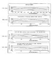
- FIGS. 4(a) to 4(d) show angular errors as observed in the resolver of the present invention and a conventional resolver.
- FIG. 4(a) shows the angular error of the prototype resolver, which was measured, by use of an R/D (resolver/digital) converter, for each reference input angle (an angle attained through an accurate rotation of the resolver by a predetermined amount by means of a rotary machine, serving as a reference).
- the error can be reduced by the following steps:
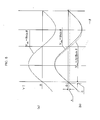
- FIG. 5 is a graph used for explaining the principle of correction according to the present invention.
- V sin has a signal waveform as shown in the lower section (b) of FIG. 5.
- This calibration step further improves the accuracy of the output voltages and the accuracy of the determined angle.
- the offset-voltage has been corrected.
- the zero points at which the output voltages become zero are expected to have deviated from correct zero points. Therefore, the shift of zero points, which has not been corrected through the above steps, is corrected through shifting by an amount corresponding to the difference G shown in FIG. 5(b). Performance of the above-described steps is expected to improve the accuracy of the output voltages and the accuracy of the determined angle.
- FIG. 4(c) is a characteristic diagram showing an angular error after adjustment of the offset voltage (in calculation).
- the maximum error (MAX) is about 60 min, which is one-fifth the maximum error of about 300 min shown in FIGS. 4(a) and 4(b).
- the minimum error (MIN) is about 25 min, which is substantially the same as the minimum error shown in FIGS. 4(a) and 4(b). Further, the obtained characteristic curve having two peaks is better than the characteristic curve having a single peak shown in FIGS. 4(a) and 4(b).
- FIG. 4(d) is a characteristic diagram showing an angular error after adjustment of the offset voltage and peak voltage (in calculation).
- FIG. 4(d) The characteristic of FIG. 4(d) is further improved as compared with that of FIG. 4(c).
- V SINOFFSET (V sin (max) + V sin (min)) / 2
- V SINAMP (V sin (max) - V sin (min)) / 2
- SINPHASE sin -1 (V SINOFFSET / V SINAMP ) ⁇ V SINOFFSET / V SINAMP )
- V COSOFFSET (V cos (max) + V cos (min)) / 2
- max is the maximum value within the positive value range
- min is the minimum value within the negative value range (sign becomes "-").
- FIGS. 6(a) to 6(c) show a graph and tables used for explaining a function F for obtaining an angle ⁇ .
- FIG. 6(a) is a graph showing the relationship between employed coil voltages and angle ranges;
- FIG. 6(b) is a table showing variables used in the function for obtaining an angle ⁇ ;
- FIG. 6(c) is a table showing variables used for obtaining an angle ⁇ ' .
- An angle ⁇ is a function of V SIN , V SIN - V SINOFFSET , V cos , V cos - V COSOFFSET , K(V cos - V COSOFFSET ), and ⁇ SINPHASE .
- the function F for obtaining an angle ⁇ is configured through modification of the variables -(V sin , V cos , ⁇ SINPHASE ) of the general formula in such a manner that in accordance with the required accuracy, the variable (V SIN - V SINOFFSET ) is used in place of the variable V sin , and the variable (V COS -V COSOFFSET ) or the variable K(V COS - V COSOFFSET ) is used in place of the variable V cos , and if necessary, a value other than zero is used for the variable ⁇ SINPHASE . This will be further described below.
- the quadrant of the rotor is determined on the basis of the resolver output voltages, the polarity of the value of sin ⁇ of the SIN coil output, and the polarity of the value of cos ⁇ of the COS coil output.
- V SIN ( ⁇ ) represents the output voltage of the SIN coil of the resolver at an angle ⁇ , and is also denoted as V SIN ⁇
- V COS ( ⁇ ) represents the output voltage of the COS coil of the resolver at an angle ⁇ , and is also denoted as V COS .
- the value of SIN ⁇ / ⁇ (radian) becomes small, so that the level or frequency of an encode signal decreases. Therefore, in an angle range not greater than 45° (0° to 45°), the output voltage V SIN ( ⁇ ) of the SIN coil of the resolver at an angle ⁇ is employed, and in an angle range greater than 45°, the output voltage V COS ( ⁇ ) of the COS coil of the resolver at an angle ⁇ is employed.
- the encode signal is a digital signal of, for example, 12 bits.
- the resolution is maintained constant, the number of bits of the encode signal increases with the dynamic range. Therefore, the dynamic range is set to an arbitrary small range; e.g., a range of sin0° to sin90°.
- a hysteresis band may be provided for the actually measured value in order to maintain the continuity of the actually measured value.
- V SINOFFSET (V sin (max) + V sin (min ) ) / 2
- V SINAMP (V sin (max) - V sin (min)) / 2
- SINPHASE sin -1 (V SINOFFSET / V SINAMP ) ⁇ V SINOFFSET / V SINAMP
- V COSOFFSET (V cos (max) + V cos (min)) / 2
- V SIN - V SINOFFSE " ⁇ SINPHASE”
- V COS - V COSOFFSET "K (V COS " V COSOFFSET )”
- V COS - V COSOFFSET and the value of "K(V COS - V COSOFFSET )" assume values equal to the actually measured value of "V COS ( ⁇ ),” "cos ⁇ ” means cos ⁇ of "Dcos ⁇ ” of an ideal form, and an angle ⁇ ' is obtained on the basis of the angle ⁇ of "cos ⁇ ” and in accordance with the computation equation in the ⁇ ' column on the left end.
- K is 1.
- V COS must be normalized with respect to V SIN in the first quadrant.
- a negative value e.g., a negative value of V COS within the range of 90° to 135°
- the absolute value thereof is obtained so as to convert the value to a positive value.
- an angle ⁇ ' is obtained by the same steps as described above.
- Zero-point correction is performed by use of the value of " ⁇ SINPHASE (radian).” That is, the value of " ⁇ SINPHASE " is added to or subtracted from the correction angle ⁇ in the above-described steps.
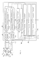
- FIG. 1 is a block diagram of an angle computation apparatus for a VR resolver according to the present invention.
- a VR resolver 8 includes a stator 9 and a rotor 10.
- a SIN voltage output coil 11, a COS voltage output coil 12, and an excitation coil 13 are provided on respective magnetic pole teeth of the stator 9.
- a voltage output from the SIN voltage output coil 11 is detected by means of an output voltage detector 14.
- a voltage output from the COS voltage output coil 12 is detected by means of an output voltage detector 15.
- Outputs of the output voltage detectors 14 and 15 are input to an angle computation apparatus 20, which outputs an angle signal ⁇ through performance of necessary computation processing.
- the angle computation apparatus 20 is formed of a microcomputer which consists of a CPU (central processing unit), memory, input/output interfaces, etc., and executes the steps described below, by means of a predetermined program.
- the program may be read from the outside or may be provided in the form of firmware.
- a table storing variables to be used with a function for obtaining an angle ⁇ and data such as resolver output voltages are stored in the memory.
- the angle computation apparatus 20 includes V sin (max) extraction means 21, V sin (min) extraction means 22, V cos (max) extraction means 23, V cos (min) extraction means 24, offset value V SINOFFSET calculation means 25, average amplitude V SINAMP calculation means 26, offset value V COSOFFSET calculation means 27, average amplitude V COSAMP calculation means 28, angle ⁇ SINPHASE calculation means 29, coefficient K calculation means 30, and angle calculation means 31.
- the angle calculation means 31 includes first angle calculation means 32, second angle calculation means 33, and third angle calculation means 34.
- the angle computation apparatus 20 is configured to perform the following steps.
- the offset V SINOFFSET calculation means 25 obtains an offset value V SINOFFSET of V sin from the values of V sin (max) and V sin (min) obtained in step (1), in accordance with the following equation Eq. 27.
- V SINOFFSET (V sin (max) + V sin (min)) / 2
- the average amplitude V SINAMP calculation means 26 calculates an average amplitude V SINAMP of V sin from the values of V sin (max) and V sin (min) obtained in step (1), in accordance with the following equation Eq. 28.
- V SINAMP (V sin (max) - V sin (min)) / 2
- the offset V COSOFFSET calculation means 27 obtains an offset value V COSOFFSET of V cos from the values of V cos (max) and V cos (min) obtained in step (2), in accordance with the following equation Eq. 29.
- V COSOFFSET (V cos (max) + V cos (min)) / 2
- the average amplitude V COSAMP calculation means 28 calculates an average amplitude V COSAMP of V cos from the values of V cos (max) and V cos (min) obtained in step (2), in accordance with the following equation Eq. 30.
- V COSAMP (V cos (max) - V cos (min)) / 2
- the angle ⁇ SINPHASE calculation means 29 calculates a zero-point correction value ⁇ SINPHASE from the offset value V SINOFFSET obtained in step (3) and the average amplitude V SINAMP obtained in step (4), in accordance with the following equation Eq. 31.
- ⁇ SINPHASE sin -1 (V SINOFFSET / V SINAMP ) ⁇ V SINOFFSET / V SINAMP
- the coefficient K calculation means 30 calculates a coefficient K from the average amplitude V SINAMP obtained in step (4) and the average amplitude V COSAMP obtained in step (6), in accordance with the following equation Eq. 32.
- K V SINAMP / V COSAMP
- the first angle calculation means 32 calculates an approximate angle ⁇ 2 from the output V SIN of the output voltage detector 14, the offset value V SINOFFSET obtained in step (3), the output V COS of the output voltage detector 15, and the offset value V COSOFFSET obtained in step (5), in accordance with the following equation Eq. 33.
- F (V sin - V SINOFFSET , (V cos - V COSOFFSET )) ⁇ 2
- the second angle calculation means 33 calculates an approximate angle ⁇ 3 from the function F ⁇ ⁇ 2 obtained in step (9) and the coefficient K obtained in step (8), in accordance with the following equation Eq. 34.
- F (V sin - V SINOFFSET , K (V cos - V COSOFFSET )) ⁇ 3
- the third angle calculation means 34 calculates an angle ⁇ 1 from the function F ⁇ ⁇ 3 obtained in step (10) and the zero-point correction value ⁇ SINPHASE obtained in step (7), in accordance with the following equation Eq. 35.
- F (V sin - V SINOFFSET , K (V cos - V COSOFFSET ), ⁇ SINPHASE ) ⁇
- angle outputs ⁇ 1 to ⁇ 3 angle outputs other than ⁇ 1 are preferably output when necessary.
- the offset values may be obtained through the following steps.
- an offset value for the sine output voltage is obtained from the deviation between an integral value of a positive output voltage and an integral value of a negative output voltage.
- an offset value for the cosine output voltage is obtained from the deviation between an integral value of a positive output voltage and an integral value of a negative output voltage.
- the apparatus can eliminate error components from the output voltages output from the resolver, to thereby improve the accuracy of angle detection.
Abstract
Description
- The present invention relates to an angle computation method for a variable reluctance resolver (hereinafter VR resolver) which enables an accurate angular detection even when unignorable errors arise from various portions of the resolver, and to an angle computation apparatus for performing the angle computation method.
- There exist a variety of resolvers, which differ in terms of operation scheme, coil structure, wiring, etc. For example, a VR resolver of a one phase excitation/two phase output includes a stator on which are wound an excitation coil, a SIN voltage output coil, and a COS voltage output coil; and a rotor which has a plurality of salient poles and which, upon rotation within the stator, changes the gap permeance between the two output coils in accordance with a sine function, which is a function of a rotational angle . The SIN voltage output coil outputs a sine output voltage, and the COS voltage output coil, which is formed with a phase difference of 90 degrees (electrical angle) with respect to the SIN voltage output coil, outputs a cosine output voltage. The sine and cosine output voltages are induced because of variation in magnetic flux upon rotation of the rotor, and the rotational position of the rotor is detected on the basis of these induced voltages.
- The stator of such a VR resolver has a large number of magnetic pole teeth. Each output voltage of the resolver is obtained as the sum total of output voltages of coils wound around corresponding magnetic pole teeth. The voltage output from the SIN voltage output coil for extracting a sine output voltage at each magnetic pole tooth is represented by α + βsin. The value of sin is determined mainly from the shape of the rotor, whereas the values of α and β are determined mainly from magnetic paths and coils of the stator. When the outputs of the respective magnetic pole teeth are represented by α1 + β1sin1, -α2+ β2sin2, ··· αm + βmsinm, the output of the resolver is represented as follows.

- The voltage output from the COS voltage output coil for extracting a cosine output voltage can be represented in an analogous manner.
- An angle detector used in a resolver and using computation means such as a microcomputer computes an angle, while using the received voltages of the resolver as they are.
- In an ideal case where the respective magnetic pole teeth have equal output amplitudes, the value of α is zero, so that the output voltage (Vsin) of the SIN voltage output coil and the output voltage (Vcos) of the COS voltage output coil can be represented as follows:
- Vsin = Bsin, and
- Vcos = Dcos.
-
- However, because of transformation ratio of resolver outputs, short circuits of output coils, run-out of the rotor, variation in magnetic characteristics among stators, variation in coils among stators, and other factors, output error increases, and an accuracy of angle detection deteriorates.
- Although such a VR resolver does not generate signals which have clear relations of sin and cos, respectively, with respect to the angular position of the shaft, it generates signals which have a high degree of reproducibility and which vary as a function of the shaft position. Angle correction has been performed through utilization of this feature. Specifically, a reference table is prepared, and sin and cos values are corrected with reference to the reference table. The VR resolver is driven at a constant speed, and distorted sine and cosine signals are recorded. These distorted signals are passed through a Fourier transformer in order to extract basic sine and cosine waves. Subsequently, these basic waves are compared with the original, distorted sine and cosine signals output from the resolver, and are used to create a correction reference table for obtaining correction values (see, for example, Japanese Patent Application Laid-Open (kokai) No. 11-51692).
- The method of obtaining proper correction values with reference to such a correction reference table has a drawback in that the table must be re-created in accordance with the details of an error, and the procedure of creating the table is complicated and time consuming.
- When output errors stemming from the above-described various causes are taken into consideration, the output voltage (Vsin) of the SIN voltage output coil and the output voltage (Vcos) of the COS voltage output coil can be represented as follows.
- In order to improve accuracy, the number of turns of coils can be adjusted such that the values of the terms "A" and "C" of Eqs. 1 and 2, which appear as output errors, become zero. However, since the number of turns cannot be increased infinitely, in some cases, the adjustment cannot reduce to zero the values of the terms "A" and "C."
Moreover, the number of turns does not necessarily become the same among individual resolvers, because of variation thereamong. - In view of the foregoing, an object of the present invention is to provide an angle computation method for a variable reluctance resolver, which method can obtain output voltages and an angle with minimized errors, through computation processing, on the basis of error-containing output voltages of the resolver.
- Another object of the present invention is to provide an angle computation apparatus for performing the angle computation method.
- The present invention employs the following means for solution in order to achieve the above object in relation to an angle computation method and apparatus for,a variable reluctance resolver.
- First, the maximum and minimum values of measured output voltages Vsin and Vcos of the resolver are obtained, the following computation is performed in order to obtain offset values A and C, and these values are stored.
- Subsequently, any one of the following means for solution (1) to (3) is employed.
- (1) The error is corrected in consideration of offsets of the output voltage of the SIN voltage output coil and the output voltage of the COS voltage output coil. An angle is obtained, while Vsin - A is used as an offset-corrected output voltage of the SIN voltage output coil for extracting sine output voltage, and Vcos - C is used as an offset-corrected output voltage of the COS voltage output coil for extracting cosine output voltage. Thus, errors in the output voltages are reduced, and angle detection accuracy is improved.
- (2) The error is corrected in consideration of the offsets
and a difference in amplitude between the output voltage of
the SIN voltage output coil and the output voltage of the COS
voltage output coil.
- (3) The error is corrected in consideration of a shift from
the zero point, the offsets, and a difference in amplitude
between the output voltage of the SIN voltage output coil and
the output voltage of the COS voltage output coil.
-
- Specifically, the present invention provides the following angle computation methods and apparatuses.
- (1) An angle computation method for a VR resolver
comprising:
- a step a of acquiring an output voltage Vsin of a SIN voltage output coil of the resolver and an output voltage Vcos of a COS voltage output coil of the resolver, and extracting the maximum value Vsin(max) of the output voltage Vsin within a range in which the output voltage Vsin assumes a positive value, the maximum value Vcos(max) of the output voltage Vcos within a range in which the output voltage Vcos assumes a positive value, the minimum value Vsin(min) of the output voltage Vsin within a range in which the output voltage Vsin assumes a negative value, the minimum value Vcos(min) of the output voltage Vcos within a range in which the output voltage Vcos assumes a negative value;
- a step b of obtaining an offset value VSINOFFSET of the output voltage Vsin from the Vsin(max) and the Vsin(min) in accordance with the following Eq. 3, and obtaining an offset value VCOSOFFSET of the output voltage Vcos from the Vcos(max) and the Vcos(min) in accordance with the following Eq. 4; and
- a step c of obtaining an angle from the output voltage
Vsin, the output voltage Vcos, the offset value VSINOFFSET, and the
offset value VCOSOFFSET in accordance with the following Eq. 5.
- (2) In the angle computation method for a VR resolver as
described in (1) above,
a step d of obtaining an average amplitude VSINAMP of the output voltage Vsin from the Vsin(max) and the Vsin (min) in accordance with the following Eq. 6, and obtaining an average amplitude VCOSAMP of the output voltage Vcos from the Vcos(max) and the Vcos(min) in accordance with the following Eq. 7, and a step e of obtaining a coefficient K from the average amplitude VSINAMP and the average amplitude VCOSAMP in accordance with the following Eq. 8 are performed between the steps b and c; and
a step f of obtaining an angle from the output voltage Vsin, the output voltage Vcos, the offset value VSINOFFSET, the offset value VCOSOFFSET, and the coefficient K in accordance with the following Eq. 9 is performed in place of the step c. - (3) In the angle computation method for a VR resolver as
described in (2) above,
a step g of obtaining an angle SINPHASE for zero-point correction from the offset value VSINOFFSET and the average amplitude VSINAMP in accordance with the following Eq. 10 is performed before or after the step e; and
a step h of obtaining an angle from the output voltage Vsin, the output voltage Vcos, the offset value VSINOFFSET, the offset value VCOSOFFSET, the coefficient K, and the angle SINPHASE in accordance with the following Eq. 11 is performed in place of the step f. - (4) An angle computation apparatus for a VR resolver
comprising:
- output voltage acquiring means for acquiring an output voltage Vsin of a SIN voltage output coil of the resolver and an output voltage Vcos of a COS voltage output coil of the resolver;
- Vsin(max) extracting means for extracting the maximum value Vsin (max) of the output voltage Vsin within a range in which the output voltage Vsin assumes a positive value;
- Vcos(max) extracting means for extracting the maximum value Vcos(max) of the output voltage Vcos within a range in which the output voltage Vcos assumes a positive value;
- Vsin(min) extracting means for extracting the minimum value Vsin(min) of the output voltage Vsin within a range in which the output voltage Vsin assumes a negative value;
- Vcos(min) extracting means for extracting the minimum value Vcos(min) of the output voltage Vcos within a range in which the output voltage Vcos assumes a negative value;
- offset value VSINOFFSET computation means for obtaining an offset value VSINOFFSET of the output voltage Vsin from the Vsin(max) and the Vsin(min) in accordance with the following Eq. 12;
- offset value VCOSOFFSET computation means for obtaining an offset value VCOSOFFSET of the output voltage Vcos from the Vcos(max) and the Vcos(min) in accordance with the following Eq. 13; and
- angle computation means for obtaining an angle from
the output voltage Vsin, the output voltage Vcos, the offset
value VSINOFFSET, and the offset value VCOSOFFSET in accordance
with the following Eq. 14.
- (5) In the angle computation apparatus for a VR resolver as
described in (4) above,
average amplitude VSINAMP computation means for obtaining an average amplitude VSINAMP of the output voltage Vsin from the Vsin(max) and the Vsin(min) in accordance with the following Eq. 15, average amplitude VCOSAMP computation means for obtaining an average amplitude VCOSAMP of the output voltage VCOS from the Vcos(max) and the Vcos(min) in accordance with the following Eq. 16, and coefficient K computation means for obtaining a coefficient K from the average amplitude VSINAMP output from the average amplitude VSINAMP computation means and the average amplitude VCOSAMP output from the average amplitude VCOSAMP computation means in accordance with the following Eq. 17 are provided between the offset value VSINOFFSET computation means and the offset value VCOSOFFSET computation means and the angle computation means; and
angle computation means for obtaining an angle from the output voltage Vsin , the output voltage Vcos, the offset value VSINOFFSET, the offset value VCOSOFFSET, and the coefficient K in accordance with the following Eq. 18 is provided in place of the angle computation means described in (4) above. - (6) In the angle computation apparatus for a VR resolver as
described in (5) above,
SINPHASE computation means for obtaining an angle SINPHASE for zero-point correction from the offset value VSINOFFSET and the average amplitude VSINAMP in accordance with the following Eq. 19 is provided; and
angle computation means for obtaining an angle from the output voltage Vsin, the output voltage Vcos, the offset value VSINOFFSET, the offset value VCOSOFFSET, the coefficient K, and the angle SINPHASE in accordance with the following Eq. 20 is provided in place of the angle computation means of (5) above. -
- The present invention can eliminate error factors from the output voltages of the output coils of the resolver to thereby improve the angle detection accuracy.
- Various other objects, features and many of the attendant advantages of the present invention will be readily appreciated as the same becomes better understood by reference to the following detailed description of the preferred embodiment when considered in connection with the accompanying drawings, in which:
- FIG. 1 is a block diagram of an angle computation apparatus for a VR resolver according to the present invention;
- FIG. 2 is a pair of waveform diagrams showing an influence of errors;
- FIG. 3 shows voltage characteristic curves based on data of a prototype resolver;
- FIGS. 4(a) to 4(d) are explanatory views showing angular errors in the resolver of the present invention, and a resolver of a conventional technique;
- FIG. 5 is a graph used for explaining the principle of correction according to the present invention; and
- FIG. 6(a) to 6(c) are a graph and tables used for explaining a function F for obtaining an angle according to the present invention.
-
- Ideally, voltage (Vsin) output from a SIN voltage output coil of a resolver and voltage (Vcos) output from a COS voltage output coil of the resolver can be expressed as follows:
- In actuality, however, the output voltages contain errors; i.e., fail to change as a function of sin or cos because of, for example, an improper rotor shape or an eccentricity of the rotor shaft. In addition, since amplitudes of the output voltages from respective magnetic pole teeth are not identical with one another, the values of the term α are non-zero, thus generating errors. Accordingly, the output voltages from the SIN voltage output coil and the COS voltage output coil are expressed as follows:
- Influences of such errors will next be described with reference to FIG. 2. FIG. 2 consists of two charts showing waveforms for explaining influences of errors. The waveforms of the output signals having different offset values (DC components) are plotted in FIG. 2(a). FIG. 2(b) shows deviations between the output signals of FIG. 2(a). Here, is the rotating angle of the rotor, and ω is the angular velocity corresponding to the frequency of an excitation signal supplied to the excitation coil.
- Of the output voltages of the resolver, the output voltage of the SIN voltage output coil for extracting a sine output voltage is represented by α + βsin(). For example, when α = 1 and β = 0.2, the output voltage is represented by (1+0.2 sin())sin(ωt). The envelope of the output voltage is represented by a line A.
- For comparison, a case where the value of α decreases from 1 to 0.9 because of another error; i.e., a case where α = 0.9 and β = 0.2, will be considered. In this case, the output voltage is represented by (0.9+0.2 sin())sin(ωt), and the envelope of the output voltage is represented by a line B.
- In order to determine the influence of the error in such a case, the deviation; i.e., the change from the characteristic represented by the line A to that represented by the line B, is studied.
- Basically, the function sin () produces the same waveform in a range of = 0 degrees to 180 degrees and in a range of = 180 degrees to 360 degrees, although its polarity changes from positive (in the former range) to negative (in the latter range). Therefore, when the waveform of sin () and the waveform of sin (+180°) are superimposed on one another, the same waveform representing the deviation between these two waveforms is repeated at an interval of every 180°.
- Here, there will considered a case where the output voltage waveforms represented by the line A and the line B, respectively, are continuously output over an angle range of 180° because of various causes of error. In order to determine the deviation over the angle range of 180°, a phase difference of 180° is provided between the output voltage waveforms represented by the line A and the line B; i.e., the output voltage waveform of the line B is represented by (0.9+0.2 sin(+180°))sin(ωt).
- The deviation between the line A and the line B is shown in FIG. 2(b). As shown in Fig. 2(b), the maximum deviation a between the lines in the 180-degree angle range of 0° to 180° of FIG. 2(a) is 0.5, whereas the maximum deviation b between the lines in the 180-degree angle range of 180° to 360° of FIG. 2(a) is 0.3. As a result, the difference G between these deviations assumes a large value of 0.2.
- As is understood from above, when the DC component changes 10% from 1 to 0.9 within an angle range of 180 degrees stemming from various causes of error, in each 180-degree angle range, the output voltage signals assume different maximum output values, and different deviations between the maximum values.
- Although the above is a study on error factors which affect the DC components, other error factors must be considered as well.
- A prototype resolver that was actually fabricated will next be described in detail.
- Table 1 shows data of the prototype resolver. SIN and COS voltage output coils are designed such that these coils produce output voltages of the same amplitude.
Data of a prototype resolver Stator 2 Transformation ratio 0.2608 Electrical error (width) 283.92 SIN COS MAX 1.948 2.001 MIN -2.105 -2.008 AMP 2.026 2.004 OFFSET -0.07822 -0.00316 - In Table 1, transformation ratio represents the ratio of the number of turns of the excitation coil to the number of turns of output coils; electrical error (width) represents the error of the resolver output voltage to the normal input voltage; MAX represents the maximum output voltage measured from the reference voltage (0 voltage) in the positive voltage region; MIN represents the minimum output voltage measured from the reference voltage (0 voltage) in the negative voltage region; AMP represents the mean value of the absolute values of MAX and MIN (AMP = (|MAX| + |MIN|) / 2); and OFFSET represents half the difference between MAX and MIN (OFFSET = (MAX + MIN) / 2).
- FIG. 3 shows voltage characteristic curves based on data of the prototype resolver. In FIG. 3, the absolute values of the voltages are plotted. Vsin is the output voltage from the SIN voltage output coil for extracting a sine output voltage. Vcos is the output voltage from the COS voltage output coil for extracting a cosine output voltage. As is clear from Table 1 and FIG. 3, the output voltage from the SIN voltage output coil and the output voltage from the COS voltage output coil differ from each other in terms of MAX, MIN, AMP, and OFFSET. In this case as well, angle ranges of about 180 degrees in which output voltages assume the positive polarity and angle ranges of about 180 degrees in which output voltages assume the negative polarity are each considered as a unit.
- Angular errors will next be described in detail. FIGS. 4(a) to 4(d) show angular errors as observed in the resolver of the present invention and a conventional resolver. FIG. 4(a) shows the angular error of the prototype resolver, which was measured, by use of an R/D (resolver/digital) converter, for each reference input angle (an angle attained through an accurate rotation of the resolver by a predetermined amount by means of a rotary machine, serving as a reference). FIG. 4(b) shows the angular error of the prototype resolver for each reference input angle, the error being computed on the basis of the voltages output from the output voltage coils. The errors are represented using the unit "min" (60 min = 1 degree). FIGS. 4(a) and 4(b) demonstrate that the angular error measured by use of the R/D converter and that computed on the basis of the output voltages generally coincide with each other. Notably, an angular error characteristic varies among prototype resolvers. In the case of the measured prototype resolver, as shown in FIGS. 4(a) and 4(b), a maximum error of about 300 min is produced near 210° and a minimum error of about 0 min is produced at 0° (360°). In one rotation cycle (360°), the error smoothly increases toward the maximum and then smoothly decreases, forming a gently sloping hill. Characteristics of the error are as follows:
- (a) Since the error reaches the maximum at 210°, the error exhibits an irregular characteristic pattern in the 360° angle range.
- (b) Since the error exhibits a profile of a gently sloping hill in each rotation cycle (360°), the error is not caused by only one factor. The error is likely generated by a plurality of factors that depend on the -rotation angle.
-
- In view of the foregoing, the error can be reduced by the following steps:
- (1) In order to eliminate the deviation, from the reference voltage, of the output voltage from the SIN voltage output coil for extracting a sine output voltage, the deviations of the maximum value (in the positive value range) and the minimum value (in the negative value range) are corrected so as to return the position of the zero point to the reference point. This is an effective method, although the positive and negative waveforms are not symmetric.
- (2) In order to eliminate the deviation, from the reference voltage, of the output voltage from the COS voltage output coil for extracting a cosine output voltage, the deviations of the maximum value (in the positive value range) and the minimum value (in the negative value range) are corrected so as to return the position of the zero point to the reference point. This is an effective method, although the positive and negative waveforms are not symmetric.
-
- The reason why the error is eliminated will next be described.
- As mentioned above, the resolver output voltage including errors originated from magnetic paths, coils, etc. can be approximated as follows:
- FIG. 5 is a graph used for explaining the principle of correction according to the present invention. The ideal sine output voltage (Vsin = Bsin) is plotted in the upper section (a) of FIG. 5.
- When the term A in Eq. 21 assumes a positive value, Vsin has a signal waveform as shown in the lower section (b) of FIG. 5.
- Specifically, the voltage varies in accordance with Bsin from a reference level, which is higher than the level of 0 volts by an offset voltage A corresponding to the value of the term A. Therefore, when the offset voltage A is subtracted from the output voltage, at least a portion of the error attributable'to the DC component can be eliminated, whereby the accuracy of the output voltages and the accuracy of an angle determined therefrom can be improved. Subsequently, in the case where the SIN voltage output coil for extracting a sine output voltage has the same number of turns as the COS voltage output coil for extracting a cosine output voltage, the output voltages of these output coils are calibrated. For such calibration, a coefficient, K = VSINAMP /VCOSAMP, is obtained. This calibration step further improves the accuracy of the output voltages and the accuracy of the determined angle. Up to these steps, the offset-voltage has been corrected. However, since the detected output voltage waveforms have irregular patterns as described in (a) and (b), the zero points at which the output voltages become zero are expected to have deviated from correct zero points.
Therefore, the shift of zero points, which has not been corrected through the above steps, is corrected through shifting by an amount corresponding to the difference G shown in FIG. 5(b). Performance of the above-described steps is expected to improve the accuracy of the output voltages and the accuracy of the determined angle. - When the above-described steps are performed in calculation, the angular error is reduced as shown in FIGS. 4(c) and 4(d). FIG. 4(c) is a characteristic diagram showing an angular error after adjustment of the offset voltage (in calculation). The maximum error (MAX) is about 60 min, which is one-fifth the maximum error of about 300 min shown in FIGS. 4(a) and 4(b). The minimum error (MIN) is about 25 min, which is substantially the same as the minimum error shown in FIGS. 4(a) and 4(b). Further, the obtained characteristic curve having two peaks is better than the characteristic curve having a single peak shown in FIGS. 4(a) and 4(b).
- FIG. 4(d) is a characteristic diagram showing an angular error after adjustment of the offset voltage and peak voltage (in calculation).
- The characteristic of FIG. 4(d) is further improved as compared with that of FIG. 4(c).
- In order to perform the following steps, the following values are calculated in advance, or when necessary, from the output voltages of the resolver and in accordance with the following equations, and are stored if necessary.
- FIGS. 6(a) to 6(c) show a graph and tables used for explaining a function F for obtaining an angle . FIG. 6(a) is a graph showing the relationship between employed coil voltages and angle ranges; FIG. 6(b) is a table showing variables used in the function for obtaining an angle ; and FIG. 6(c) is a table showing variables used for obtaining an angle ' .
- Variables which are used in the function for obtaining an angle and which are used in the following description are provided in the form of a table shown in FIG. 6(b). An angle is a function of VSIN, VSIN - VSINOFFSET, Vcos, Vcos - VCOSOFFSET, K(Vcos - VCOSOFFSET), and SINPHASE. The general formula can be represented by the following Eq. 23.
- In the leftmost column of the table, there are listed values of an angle serving as a reference (hereinafter referred to as a reference angle ) and being continuously changed at an arbitrary change rate within the range between 0° to 90°. In each row, the following items (1) to (8) corresponding to the reference angle are listed:
- (1) sin;
- (2) actually measured voltage Vsin of the SIN coil (i.e., actually measured voltage such that when the actual value is represented by Bsin (ideal form), the value of corresponds to the reference angle );
- (3) corrected voltage (VSIN - VSINOFFSET) obtained through correction of the actually measured voltage of the SIN coil by use of an offset voltage (i.e., the'voltage (VSIN - VSINOFFSET) such that when the voltage (VSIN - VSINOFFSET ) is represented by Bsin (ideal form), the value of corresponds to the reference angle );
- (4) angle SINPHASE (zero-point correction angle after correction of the actually measured voltage Vsin of the SIN coil by use of an offset voltage; i.e., the zero-point correction angle determined such that when the corrected voltage (VSIN - VSINOFFSET) is represented by Bsin (ideal form), the value of corresponds to the reference angle );
- (5) cos;
- (6) actually measured voltage Vcos of the COS coil (i.e., actually measured voltage such that when the actual value is represented by Dcos (ideal form), the value of corresponds to the reference angle );
- (7) corrected voltage (VCOS - VCOSOFFSET) obtained through correction of the actually measured voltage of the COS coil by use of an offset voltage (i.e., the voltage (VCOS - VCOSOFFSET) such that when the voltage (VCOS - VCOSOFFSET) is represented by Dcos (ideal form), the value of corresponds to the reference angle ); and
- (8) voltage K(VCOS - VCOSOFFSET) obtained through normalization of the corrected voltage (VCOS - VCOSOFFSET) by use of a normalization coefficient K for normalizing the output voltage of the COS coil with respect to the output voltage of the SIN coil (i.e., the voltage K(VCOS - VCOSOFFSET) determined such that when the voltage K(VCOS - VCOSOFFSET) is represented by Dcos (ideal form), the value of corresponds to the reference angle ).
-
- The function F for obtaining an angle is configured through modification of the variables -(Vsin, Vcos, SINPHASE) of the general formula in such a manner that in accordance with the required accuracy, the variable (VSIN - VSINOFFSET) is used in place of the variable Vsin, and the variable (VCOS-VCOSOFFSET) or the variable K(VCOS - VCOSOFFSET) is used in place of the variable Vcos, and if necessary, a value other than zero is used for the variable SINPHASE. This will be further described below.
- The quadrant of the rotor is determined on the basis of the resolver output voltages, the polarity of the value of sin of the SIN coil output, and the polarity of the value of cos of the COS coil output.
First Quadrant VSIN() ≥ 0, VCOS() ≥ 0 Second Quadrant VSIN() ≥ 0, VCOS() < 0 Third Quadrant VSIN() < 0, VCOS() < 0 Fourth Quadrant VSIN() < 0, VCOS() > 0 - Respective quadrants will be described.
- For example, when the angle is equal to or greater than 45° (45° to 90°) in the first quadrant, the value of SIN/ (radian) becomes small, so that the level or frequency of an encode signal decreases. Therefore, in an angle range not greater than 45° (0° to 45°), the output voltage VSIN() of the SIN coil of the resolver at an angle is employed, and in an angle range greater than 45°, the output voltage VCOS() of the COS coil of the resolver at an angle is employed.
- The encode signal is a digital signal of, for example, 12 bits. When the resolution is maintained constant, the number of bits of the encode signal increases with the dynamic range. Therefore, the dynamic range is set to an arbitrary small range; e.g., a range of sin0° to sin90°.
- Notably, in the case where the actually measured value of the output voltage VSIN() does not increase or decrease continuously because of measurement error or other factors, a hysteresis band may be provided for the actually measured value in order to maintain the continuity of the actually measured value.
- In the remaining second, third, and fourth quadrants, when the value of VSIN() or VCOS() is negative, its absolute value is obtained in order to convert the negative value to a positive value, and then the table of the function F for obtaining an angle is searched.
- Through the above-described procedures, the relationship between to-be-employed coil voltages and angle ranges are set as indicated by hatching in FIG. 6(a). For convenience, other quadrants will be described.
Angle Employed Voltage 0° to 45° VSIN() 45° to 90° V COS()90° to 135° VCOS() 135° to 180° V SIN()180° to 225° VSIN() 225° to 270° V COS()270° to 315° VCOS() 315° to 360° VSIN() - Next, on the basis of Table 3, in the angle range of, for example, 0° to 45°, an actually measured value of VSIN() is represented by B'sin (ideal form). Similarly, in the angle range of, for example, 45° to 90°, an actually measured value of VCOS() is represented by Dcos (ideal form). Subsequently, in accordance with the required accuracy, the following values are calculated and stored.
- Subsequently, as shown in FIG. 6(b), the following values are obtained in accordance with the accuracy. Notably, VSIN = VSIN() and VCOS = VCOS().
"VSIN - VSINOFFSE"
"SINPHASE "
"VCOS - VCOSOFFSET"
"K (VCOS " VCOSOFFSET)" - Each row of the table of FIG. 6(b) shows the following. As to the output of the SIN coil, the value of "VSIN - VSINOFFSET," assumes a value equal to the actually measured value of "VSIN()", "sin" means sin of "Bsin" of an ideal form, and an angle ' is obtained on the basis of the angle of "sin" and in accordance with the computation equation in the ' column at the left end. As to the output of the COS coil, the value of "VCOS - VCOSOFFSET" and the value of "K(VCOS - VCOSOFFSET)" assume values equal to the actually measured value of "VCOS()," "cos" means cos of "Dcos" of an ideal form, and an angle ' is obtained on the basis of the angle of "cos" and in accordance with the computation equation in the ' column on the left end. Ideally, K is 1. In actuality, since VSIN and VCOS have different amplitudes in each quadrant, VCOS must be normalized with respect to VSIN in the first quadrant.
- Next, there will be described the steps for obtaining an angle ' through searching the above-described table of the function F of an angle .
- In the angle range of, for example, 0° to 45°, when the value of "VSIN - VSINOFFSET" obtained in accordance with the accuracy becomes equal to the actually measured value of "VSIN() , " an angle corresponding to the sin of "Bsin" represents an angle ' to be obtained.
- In the angle range of, for example, 45° to 90°, when the value of "VCOS - VCOSOFFSET" or the value of "K(VCOS - VCOSOFFSET)" obtained in accordance with the accuracy becomes equal to the actually measured value of "VCOS()," an angle corresponding to the sin of Bsin corresponding to the value of the above-described Dcos is obtained, and an angle ' is obtained by subtracting from 90° (angle ' = 90° - ).
- The reason why the angle ' is obtained in the above-described manner is that, as shown in FIG. 6(a), in the angle range of 45° to 90°, the value of sin increases, but the value of cos decreases. If this cos is used in place of the sin value, the obtained angle decreases from 45° toward 0°. In order to attain an increase instead of such a decrease and in order not to increase the range of the encode signal, an angle is obtained by use of the value of sin0° to sin45°. Accordingly, the angle ' is obtained by subtracting from 90° (angle ' = 90° - ).
- For a negative value; e.g., a negative value of VCOS within the range of 90° to 135°, the absolute value thereof is obtained so as to convert the value to a positive value. Subsequently, an angle ' is obtained by the same steps as described above.
- Zero-point correction is performed by use of the value of "SINPHASE (radian)." That is, the value of "SINPHASE " is added to or subtracted from the correction angle in the above-described steps.
- Next, there will be described steps which are performed in accordance with the required accuracy.
- Step 1: The error is corrected in consideration of offsets
of the output voltage of the SIN voltage output coil and the
output voltage of the COS voltage output coil. The above-described
OFFSET values; i.e., offset components (DC
components) VSINOFFSET and VCOSOFFSET are obtained from the output
voltage, and then the computation equation for obtaining an
angle from the resolver signals is corrected by use of the
OFFSET values as shown in the following Eq. 24, to thereby
improve computation accuracy. Notably, the value of "SINPHASE"
is set to zero.
- Step 2: The error is corrected in consideration of offsets,
a difference in amplitude between the output voltage of the
SIN voltage output coil and the output voltage of the COS
voltage output coil.
-
- FIG. 1 is a block diagram of an angle computation apparatus for a VR resolver according to the present invention.
- A VR resolver 8 includes a
stator 9 and arotor 10. - A SIN
voltage output coil 11, a COSvoltage output coil 12, and anexcitation coil 13 are provided on respective magnetic pole teeth of thestator 9. When the rotary shaft is rotated with theexcitation coil 13 excited, a voltage output from the SINvoltage output coil 11 is detected by means of anoutput voltage detector 14. Similarly, a voltage output from the COSvoltage output coil 12 is detected by means of anoutput voltage detector 15. - Outputs of the
output voltage detectors angle computation apparatus 20, which outputs an angle signal through performance of necessary computation processing. - The
angle computation apparatus 20 is formed of a microcomputer which consists of a CPU (central processing unit), memory, input/output interfaces, etc., and executes the steps described below, by means of a predetermined program. The program may be read from the outside or may be provided in the form of firmware. A table storing variables to be used with a function for obtaining an angle and data such as resolver output voltages are stored in the memory. - The
angle computation apparatus 20 includes Vsin(max) extraction means 21, Vsin(min) extraction means 22, Vcos(max) extraction means 23, Vcos(min) extraction means 24, offset value VSINOFFSET calculation means 25, average amplitude VSINAMP calculation means 26, offset value VCOSOFFSET calculation means 27, average amplitude VCOSAMP calculation means 28, angle SINPHASE calculation means 29, coefficient K calculation means 30, and angle calculation means 31. The angle calculation means 31 includes first angle calculation means 32, second angle calculation means 33, and third angle calculation means 34. - The
angle computation apparatus 20 is configured to perform the following steps. - The Vsin(max) extraction means 21 samples the output (Vsin = A + Bsin) of the
output voltage detector 14, extracts Vsin(max), and stores the same. Similarly, the Vsin(min) extraction means 22 samples the output (Vsin = A + Bsin) of theoutput voltage detector 14, extracts Vsin(min), and stores the same. - The Vcos(max) extraction means 23 samples the output (Vcos = C + Dcos) of the
output voltage detector 15, extracts Vcos(max), and stores the same. Similarly, the Vcos(min) extraction means 24 samples the output (Vcos = C + Dcos) of theoutput voltage detector 15, extracts Vcos(min), and stores the same. - The offset VSINOFFSET calculation means 25 obtains an offset value VSINOFFSET of Vsin from the values of Vsin(max) and Vsin(min) obtained in step (1), in accordance with the following equation Eq. 27.
- The average amplitude VSINAMP calculation means 26 calculates an average amplitude VSINAMP of Vsin from the values of Vsin(max) and Vsin(min) obtained in step (1), in accordance with the following equation Eq. 28.
- The offset VCOSOFFSET calculation means 27 obtains an offset value VCOSOFFSET of Vcos from the values of Vcos(max) and Vcos(min) obtained in step (2), in accordance with the following equation Eq. 29.
- The average amplitude VCOSAMP calculation means 28 calculates an average amplitude VCOSAMP of Vcos from the values of Vcos(max) and Vcos(min) obtained in step (2), in accordance with the following equation Eq. 30.
- The angle SINPHASE calculation means 29 calculates a zero-point correction value SINPHASE from the offset value VSINOFFSET obtained in step (3) and the average amplitude VSINAMP obtained in step (4), in accordance with the following equation Eq. 31.
- The coefficient K calculation means 30 calculates a coefficient K from the average amplitude VSINAMP obtained in step (4) and the average amplitude VCOSAMP obtained in step (6), in accordance with the following equation Eq. 32.
- The first angle calculation means 32 calculates an approximate angle 2 from the output VSIN of the
output voltage detector 14, the offset value VSINOFFSET obtained in step (3), the output VCOS of theoutput voltage detector 15, and the offset value VCOSOFFSET obtained in step (5), in accordance with the following equation Eq. 33. - The second angle calculation means 33 calculates an approximate angle 3 from the function F ≅ 2 obtained in step (9) and the coefficient K obtained in step (8), in accordance with the following equation Eq. 34.
- The third angle calculation means 34 calculates an angle 1 from the function F ≅ 3 obtained in step (10) and the zero-point correction value SINPHASE obtained in step (7), in accordance with the following equation Eq. 35.
- The above-described steps may be slightly shifted so long as computation is not hindered. Among the angle outputs 1 to 3, angle outputs other than 1 are preferably output when necessary.
- Through execution of the above-described steps, the angular error characteristics shown in FIGS. 4(c) and 4(d) can be attained. Thus, the angular error can be reduced greatly.
- The offset values may be obtained through the following steps.
- For the SIN voltage output coil for extracting the sine output voltage, an offset value for the sine output voltage is obtained from the deviation between an integral value of a positive output voltage and an integral value of a negative output voltage. Similarly, for the COS voltage output coil for extracting the cosine output voltage, an offset value for the cosine output voltage is obtained from the deviation between an integral value of a positive output voltage and an integral value of a negative output voltage. Subsequently, the above-described correction of offset voltages (DC components) is performed by use of these offset values.
- In this case as well, the apparatus can eliminate error components from the output voltages output from the resolver, to thereby improve the accuracy of angle detection.
- Obviously, numerous modifications and variations of the present invention are possible in light of the above teachings. It is therefore to be understood that within the scope of the appended claims, the present invention may be practiced otherwise than as specifically described herein.
- The features disclosed in the foregoing description, in the claim and/or in the accompanying drawings may, both separately and in any combination thereof, be material for realising the invention in diverse forms thereof.
Claims (6)
- An angle computation method for a VR resolver comprising:a step a of acquiring an output voltage Vsin of a SIN voltage output coil of the resolver and an output voltage Vcos of a COS voltage output coil of the resolver , and extracting the maximum value Vsin(max) of the output voltage Vsin within a range in which the output voltage Vsin assumes a positive value, the maximum value Vcos(max) of the output voltage Vcos within a range in which the output voltage Vcos assumes a positive value, the minimum value Vsin(min) of the output voltage Vsin within a range in which the output voltage Vsin assumes a negative value, the minimum value Vcos(min) of the output voltage Vcos within a range in which the output voltage Vcos assumes a negative value;a step b of obtaining an offset value VSINOFFSET of the output voltage Vsin from the Vsin(max) and the Vsin(min) in accordance with Eq. A, and obtaining an offset value VCOSOFFSET of the output voltage Vcos from the Vcos(max) and the Vcos(min) in accordance with Eq. B; anda step c of obtaining an angle from the output voltage Vsin, the output voltage Vcos, the offset value VSINOFFSET, and the offset value VCOSOFFSET in accordance with Eq. C.
- An angle computation method for a VR resolver according to claim 1, wherein
a step d of obtaining an average amplitude VSINAMP of the output voltage Vsin from the Vsin(max) and the Vsin(min) in accordance with Eq. D, and obtaining an average amplitude VCOSAMP of the output voltage Vcos from the Vcos(max) and the Vcos(min) in accordance with Eq. E, and a step e of obtaining a coefficient K from the average amplitude VSINAMP and the average amplitude VCOSAMP in accordance with Eq. F are performed between the steps b and c; and
a step f of obtaining an angle from the output voltage Vsin, the output voltage Vcos, the offset value VSINOFFSET, the offset value VCOSOFFSET, and the coefficient K in accordance with Eq. G is performed in place of the step c. - An angle computation method for a VR resolver according to claim 2, wherein
a step g of obtaining an angle SINPHASE for zero-point correction from the offset value VSINOFFSET and the average amplitude VSINAMP in accordance with Eq. H is performed before or after the step e; and
a step h of obtaining an angle from the output voltage Vsin, the output voltage Vcos, the offset value VSINOFFSET, the offset value VCOSOFFSET , the coefficient K, and the angle SINPHASE in accordance with Eq. I is performed in place of the step f. - An angle computation apparatus for a VR resolver comprising:output voltage acquiring means for acquiring an output voltage Vsin of a SIN voltage output coil of the resolver and an output voltage Vcos of a COS voltage output coil of the resolver;Vsin(max) extracting means for extracting the maximum value Vsin(max) of the output voltage Vsin within a range in which the output voltage Vsin assumes a positive value;Vcos(max) extracting means for extracting the maximum value Vcos(max) of the output voltage Vcos within a range in which the output voltage Vcos assumes a positive value;Vsin(min) extracting means for extracting the minimum value Vsin(min) of the output voltage Vsin within a range in which the output voltage Vsin assumes a negative value;Vcos(min) extracting means for extracting the minimum value Vcos(min) of the output voltage Vcos within a range in which the output voltage Vcos assumes a negative value;offset value VSINOFFSET computation means for obtaining an offset value VSINOFFSET of the output voltage Vsin from the Vsin(max) and the Vsin(min) in accordance with Eq. A;offset value VCOSOFFSET computation means for obtaining an offset value VCOSOFFSET of the output voltage Vcos from the Vcos(max) and the Vcos (min) in accordance with Eq. B; andangle computation means for obtaining an angle from the output voltage Vsin, the output voltage Vcos, the offset value VSINOFFSET, and the offset value VCOSOFFSET in accordance with Eq. C.
- An angle computation apparatus for a VR resolver according to claim 4, wherein
average amplitude VSINAMP computation means for obtaining an average amplitude VSINAMP of the output voltage Vsin from the Vsin(max) and the Vsin(min) in accordance with Eq. D, average amplitude VCOSAMP computation means for obtaining an average amplitude VCOSAMP of the output voltage Vcos from the Vcos(max) and the Vcos(min) in accordance with Eq. E, and coefficient K computation means for obtaining a coefficient K from the average amplitude VSINAMP output from the average amplitude VSINAMP computation means and the average amplitude VCOSAMP output from the average amplitude VCOSAMP computation means in accordance with Eq. F are provided between the offset value VSINOFFSET computation means and the offset value VCOSOFFSET computation means and the angle computation means; and
angle computation means for obtaining an angle from the output voltage Vsin, the output voltage Vcos, the offset value VSINOFFSET, the offset value VCOSOFFSET, and the coefficient K in accordance with Eq. G is provided in place of the angle computation means of claim 4. - An angle computation apparatus for a VR resolver according to claim 5, wherein
SINPHASE computation means for obtaining an angle SINPHASE for zero-point correction from the offset value VSINOFFSET and the average amplitude VSINAMP in accordance with Eq. H is provided; and
angle computation means for obtaining an angle from the output voltage Vsin, the output voltage Vcos, the offset value VSINOFFSET, the offset value VCOSOFFSET, the coefficient K, and the angle SINPHASE in accordance with Eq. I is provided in place of the angle computation means of claim 5.
Applications Claiming Priority (4)
| Application Number | Priority Date | Filing Date | Title |
|---|---|---|---|
| JP2003424204 | 2003-12-22 | ||
| JP2003424204 | 2003-12-22 | ||
| JP2004118722 | 2004-04-14 | ||
| JP2004118722A JP2005208028A (en) | 2003-12-22 | 2004-04-14 | Angle operation method for variable reluctance resolver, and angle operation unit for the same |
Publications (2)
| Publication Number | Publication Date |
|---|---|
| EP1551095A2 true EP1551095A2 (en) | 2005-07-06 |
| EP1551095A3 EP1551095A3 (en) | 2007-03-21 |
Family
ID=34576004
Family Applications (1)
| Application Number | Title | Priority Date | Filing Date |
|---|---|---|---|
| EP04014514A Withdrawn EP1551095A3 (en) | 2003-12-22 | 2004-06-21 | Angle computation method and apparatus for variable reluctance resolver |
Country Status (3)
| Country | Link |
|---|---|
| US (1) | US7187309B2 (en) |
| EP (1) | EP1551095A3 (en) |
| JP (1) | JP2005208028A (en) |
Cited By (2)
| Publication number | Priority date | Publication date | Assignee | Title |
|---|---|---|---|---|
| EP2108924A3 (en) * | 2008-04-07 | 2013-03-27 | Denso Corporation | Position detecting device and method |
| EP2543975A4 (en) * | 2010-03-03 | 2015-08-26 | Jtekt Corp | Angle of rotation detetction device |
Families Citing this family (16)
| Publication number | Priority date | Publication date | Assignee | Title |
|---|---|---|---|---|
| WO2007137625A1 (en) * | 2006-06-01 | 2007-12-06 | Freescale Semiconductor, Inc. | Sin-cos sensor arrangement, integrated circuit and method therefor |
| JP5079346B2 (en) | 2007-01-30 | 2012-11-21 | 東芝機械株式会社 | Waveform correction apparatus and waveform correction method |
| US20080189072A1 (en) * | 2007-02-01 | 2008-08-07 | Nescom Inc. | High resolution encoder within a swivel |
| JP2008273478A (en) * | 2007-05-07 | 2008-11-13 | Mitsubishi Electric Corp | Electric power steering control device |
| DE102008010964A1 (en) * | 2008-02-25 | 2009-08-27 | Continental Automotive Gmbh | Method of operating an actuator and actuator |
| KR101012740B1 (en) * | 2009-04-28 | 2011-02-09 | 경상대학교산학협력단 | Resolver digital converter and position detecting apparatus |
| JP2012068156A (en) * | 2010-09-24 | 2012-04-05 | Denso Corp | Sensor device |
| JP2012093215A (en) * | 2010-10-27 | 2012-05-17 | Omron Automotive Electronics Co Ltd | Rotation angle detecting device |
| KR101905297B1 (en) * | 2014-06-13 | 2018-10-05 | 미쓰비시덴키 가부시키가이샤 | Digital protection relay |
| US9897469B2 (en) * | 2016-01-26 | 2018-02-20 | GM Global Technology Operations LLC | Resolver phase compensation |
| JP6705314B2 (en) * | 2016-07-05 | 2020-06-03 | 株式会社デンソー | Steering control device |
| JP7251751B2 (en) * | 2017-11-07 | 2023-04-04 | 株式会社松尾製作所 | Electrical angle acquisition system, electrical angle acquisition method, electrical angle acquisition program, electrical angle acquisition characteristic measurement system, electrical angle acquisition characteristic measurement method, and electrical angle acquisition characteristic measurement program |
| JP2019219247A (en) * | 2018-06-19 | 2019-12-26 | 株式会社デンソー | Resolver signal processing circuit |
| CN110793553B (en) * | 2019-11-07 | 2021-07-23 | 歌尔股份有限公司 | Zero point positioning method, system, servo motor and storage medium |
| CN112504115B (en) * | 2020-11-17 | 2023-05-09 | 中国电子科技集团公司第三十八研究所 | Detection device and method for double-channel rotary-variable mounting flatness on turntable |
| CN113271043B (en) * | 2021-05-26 | 2022-12-23 | 永大电梯设备(中国)有限公司 | Method for correcting angle deviation between rotor of rotary transformer and rotor of permanent magnet synchronous motor |
Citations (2)
| Publication number | Priority date | Publication date | Assignee | Title |
|---|---|---|---|---|
| EP0599175A1 (en) * | 1992-11-27 | 1994-06-01 | Sony Magnescale, Inc. | Interpolation device for scale arrangement |
| EP0877464A2 (en) * | 1997-05-09 | 1998-11-11 | Kollmorgen Corporation | Variable reluctance resolver to digital converter |
Family Cites Families (3)
| Publication number | Priority date | Publication date | Assignee | Title |
|---|---|---|---|---|
| US5645065A (en) * | 1991-09-04 | 1997-07-08 | Navion Biomedical Corporation | Catheter depth, position and orientation location system |
| US6885927B2 (en) * | 2002-04-17 | 2005-04-26 | Honda Giken Kogyo Kabushiki Kaisha | Apparatus for controlling an electric power steering system |
| JP4604551B2 (en) * | 2003-09-24 | 2011-01-05 | 株式会社ジェイテクト | Resolver signal arithmetic processing method and arithmetic processing apparatus |
-
2004
- 2004-04-14 JP JP2004118722A patent/JP2005208028A/en active Pending
- 2004-06-15 US US10/866,804 patent/US7187309B2/en not_active Expired - Fee Related
- 2004-06-21 EP EP04014514A patent/EP1551095A3/en not_active Withdrawn
Patent Citations (2)
| Publication number | Priority date | Publication date | Assignee | Title |
|---|---|---|---|---|
| EP0599175A1 (en) * | 1992-11-27 | 1994-06-01 | Sony Magnescale, Inc. | Interpolation device for scale arrangement |
| EP0877464A2 (en) * | 1997-05-09 | 1998-11-11 | Kollmorgen Corporation | Variable reluctance resolver to digital converter |
Cited By (2)
| Publication number | Priority date | Publication date | Assignee | Title |
|---|---|---|---|---|
| EP2108924A3 (en) * | 2008-04-07 | 2013-03-27 | Denso Corporation | Position detecting device and method |
| EP2543975A4 (en) * | 2010-03-03 | 2015-08-26 | Jtekt Corp | Angle of rotation detetction device |
Also Published As
| Publication number | Publication date |
|---|---|
| EP1551095A3 (en) | 2007-03-21 |
| US20050132802A1 (en) | 2005-06-23 |
| US7187309B2 (en) | 2007-03-06 |
| JP2005208028A (en) | 2005-08-04 |
Similar Documents
| Publication | Publication Date | Title |
|---|---|---|
| EP1551095A2 (en) | Angle computation method and apparatus for variable reluctance resolver | |
| US6239571B1 (en) | Resolver | |
| US7088025B2 (en) | Variable-reluctance resolver and rotational angle sensor using same | |
| EP0748039A2 (en) | Rotation position detecting device and motor device | |
| US11397098B2 (en) | Method for detecting errors in a rotating position sensor system having sine and cosine signals | |
| JP5173962B2 (en) | Resolver / digital conversion apparatus and resolver / digital conversion method | |
| US20020011814A1 (en) | Pole position detector for motor | |
| US7030532B2 (en) | Variable reluctance resolver | |
| JP2558159B2 (en) | Two-phase signal generator and two-phase signal generation method | |
| EP4047323A1 (en) | Inductive angular sensor method and system | |
| CN111464107B (en) | Motor, motor data analysis method, device and system | |
| KR20170125723A (en) | Angle determinating method using encoder signal with noise suppression, adjusting method for output signal of encoder and absolute encoder | |
| US8278915B2 (en) | Minimizing magnetic interference in a variable reluctance resolver | |
| JP3309027B2 (en) | Reluctant resolver | |
| CN112880725A (en) | Method for judging total pitch deviation of position sensor | |
| CN110506196A (en) | Position detecting device and method for detecting position | |
| JP2000258187A (en) | Device for detecting zero location of variable reluctance-type resolver | |
| JP2000046584A (en) | Position detector | |
| US11909282B2 (en) | Device, arrangement and method for determining an angle between a rotor and a stator | |
| EP1016852A1 (en) | Apparatus for measuring the position of a movable member | |
| JP2002048508A (en) | Detector for relative rotational position | |
| US11555716B1 (en) | Harmonic compensation with magnitude feedback for magnetic field sensors | |
| JPH0356819A (en) | Rotation angle detecting device | |
| EP4170287A1 (en) | Circuit and method for determining angular position | |
| JPH08285636A (en) | Rotation angle detector |
Legal Events
| Date | Code | Title | Description |
|---|---|---|---|
| PUAI | Public reference made under article 153(3) epc to a published international application that has entered the european phase |
Free format text: ORIGINAL CODE: 0009012 |
|
| AK | Designated contracting states |
Kind code of ref document: A2 Designated state(s): AT BE BG CH CY CZ DE DK EE ES FI FR GB GR HU IE IT LI LU MC NL PL PT RO SE SI SK TR |
|
| AX | Request for extension of the european patent |
Extension state: AL HR LT LV MK |
|
| PUAL | Search report despatched |
Free format text: ORIGINAL CODE: 0009013 |
|
| AK | Designated contracting states |
Kind code of ref document: A3 Designated state(s): AT BE BG CH CY CZ DE DK EE ES FI FR GB GR HU IE IT LI LU MC NL PL PT RO SE SI SK TR |
|
| AX | Request for extension of the european patent |
Extension state: AL HR LT LV MK |
|
| RIC1 | Information provided on ipc code assigned before grant |
Ipc: G01D 5/244 20060101ALI20070215BHEP Ipc: G01D 5/20 20060101ALI20070215BHEP Ipc: H02K 24/00 20060101AFI20050517BHEP |
|
| AKX | Designation fees paid |
Designated state(s): DE FR GB IT |
|
| STAA | Information on the status of an ep patent application or granted ep patent |
Free format text: STATUS: THE APPLICATION IS DEEMED TO BE WITHDRAWN |
|
| 18D | Application deemed to be withdrawn |
Effective date: 20070922 |