EP4112315B1 - Method for controlling regenerated chip, regenerated chip and regenerated ink cartridge - Google Patents
Method for controlling regenerated chip, regenerated chip and regenerated ink cartridge Download PDFInfo
- Publication number
- EP4112315B1 EP4112315B1 EP21822814.6A EP21822814A EP4112315B1 EP 4112315 B1 EP4112315 B1 EP 4112315B1 EP 21822814 A EP21822814 A EP 21822814A EP 4112315 B1 EP4112315 B1 EP 4112315B1
- Authority
- EP
- European Patent Office
- Prior art keywords
- chip
- data signal
- ink cartridge
- regenerated
- operation command
- Prior art date
- Legal status (The legal status is an assumption and is not a legal conclusion. Google has not performed a legal analysis and makes no representation as to the accuracy of the status listed.)
- Active
Links
Images



Classifications
-
- B—PERFORMING OPERATIONS; TRANSPORTING
- B41—PRINTING; LINING MACHINES; TYPEWRITERS; STAMPS
- B41J—TYPEWRITERS; SELECTIVE PRINTING MECHANISMS, i.e. MECHANISMS PRINTING OTHERWISE THAN FROM A FORME; CORRECTION OF TYPOGRAPHICAL ERRORS
- B41J2/00—Typewriters or selective printing mechanisms characterised by the printing or marking process for which they are designed
- B41J2/005—Typewriters or selective printing mechanisms characterised by the printing or marking process for which they are designed characterised by bringing liquid or particles selectively into contact with a printing material
- B41J2/01—Ink jet
- B41J2/17—Ink jet characterised by ink handling
- B41J2/175—Ink supply systems ; Circuit parts therefor
-
- B—PERFORMING OPERATIONS; TRANSPORTING
- B41—PRINTING; LINING MACHINES; TYPEWRITERS; STAMPS
- B41J—TYPEWRITERS; SELECTIVE PRINTING MECHANISMS, i.e. MECHANISMS PRINTING OTHERWISE THAN FROM A FORME; CORRECTION OF TYPOGRAPHICAL ERRORS
- B41J2/00—Typewriters or selective printing mechanisms characterised by the printing or marking process for which they are designed
- B41J2/005—Typewriters or selective printing mechanisms characterised by the printing or marking process for which they are designed characterised by bringing liquid or particles selectively into contact with a printing material
- B41J2/01—Ink jet
- B41J2/17—Ink jet characterised by ink handling
- B41J2/175—Ink supply systems ; Circuit parts therefor
- B41J2/17503—Ink cartridges
- B41J2/17543—Cartridge presence detection or type identification
- B41J2/17546—Cartridge presence detection or type identification electronically
-
- B—PERFORMING OPERATIONS; TRANSPORTING
- B41—PRINTING; LINING MACHINES; TYPEWRITERS; STAMPS
- B41J—TYPEWRITERS; SELECTIVE PRINTING MECHANISMS, i.e. MECHANISMS PRINTING OTHERWISE THAN FROM A FORME; CORRECTION OF TYPOGRAPHICAL ERRORS
- B41J2/00—Typewriters or selective printing mechanisms characterised by the printing or marking process for which they are designed
- B41J2/005—Typewriters or selective printing mechanisms characterised by the printing or marking process for which they are designed characterised by bringing liquid or particles selectively into contact with a printing material
- B41J2/01—Ink jet
- B41J2/17—Ink jet characterised by ink handling
- B41J2/175—Ink supply systems ; Circuit parts therefor
- B41J2/17503—Ink cartridges
Definitions
- the present invention relates to the field of a printer, and in particular, to a regenerated chip, a regenerated ink cartridge, and a method for controlling the regenerated chip.
- a data signal wire of a printer can be used to read data stored in a chip of an original ink cartridge, which can be data of a selected storage unit, except when the data stored in the chip of the original ink cartridge is no longer available. Therefore, it is necessary to stop communication through the data signal wire between the printer and the original ink cartridge and directly connect the regenerated chip to the printer through a communication signal wire. As such when the printer reads data of a data storage area of the chip of the original ink cartridge, the DATA signal can only enter a data area of the regenerated chip to read data stored in the regenerated chip.
- the DATA signal is not only configured to read the data of the data storage area of the chip of the original ink cartridge, but also has other functions, such as a function of a logic signal of controlling selection of a print spot of the ink cartridge. Therefore, stopping a DATA signal communication between the printer and the original ink cartridge would affect other important functions including the selection of the print spot of the ink cartridge when an upgraded printer prints, and affect printing effect, resulting in poor printing quality of the printer with the regenerated chip.
- CN207669999U discloses a kind of regeneration chip component of printing consumables, including: original-pack chip, compatible chip and the control chip being connect respectively with printer.
- the control chip is also connected to the original-pack chip and the compatible chip respectively, so that the control chip is controlled according to the enable signal of the printer received, the original-pack chip, the compatible chip is in running order or/reset state of awaiting orders.
- EP3395577 A1 discloses a repair method and repair chip for a regenerative ink cartridge, and a regenerative ink cartridge.
- the repair chip does not need to monitor all lines of a printer and only needs to monitor an enable line, a data line and auxiliary lines of the printer, so that the number of pads, electrically connected with the printer, of an original chip is reduced, the welding difficulty and workload in the ink cartridge regeneration process are lowered accordingly, and the risk of ink cartridge scraping in the repair process is lowered from the source.
- a regenerated chip, and a regenerated ink cartridge, and a method for controlling the regenerated chip are provided to solve a problem of poor printing quality of the printer with the regenerated chip in the related art.
- the present invention provides the method for controlling the regenerated chip.
- the regenerated chip is electrically connected to a printer by means of a first data signal wire and a logic signal wire, and is electrically connected to an ink cartridge chip by means of a second data signal wire.
- the method includes: detecting an operation command sent by the printer by means of the first data signal wire and the logic signal wire; and when it is detected that the operation command is not a selected operation command, sending a data signal to the ink cartridge chip by means of the second data signal wire.
- the data signal is configured to instruct the ink cartridge chip to communicate with the printer.
- the method further includes: when it is detected that the operation command is the selected operation command, controlling the second data signal wire to be turned off and feeding back storage data to the printer by means of the first data signal wire.
- the method before the sending the data signal to the ink cartridge chip by means of the second data signal wire, the method further includes: detecting a feedback voltage between a first storage module of the regenerated chip and a second storage module of the ink cartridge chip; sending the data signal to the ink cartridge chip when the feedback voltage is greater than or equal to a preset voltage; and controlling the second data signal wire to be turned off when the feedback voltage is less than the preset voltage.
- the first storage module and the second storage module are connected in parallel.
- the method further includes: when it is detected that the operation command is not the selected operation command or the feedback voltage is greater than or equal to the preset voltage, sending the data signal to the ink cartridge chip; and when the selected operation command is detected and the feedback voltage is less than the preset voltage, controlling the second data signal wire to be turned off.
- the method further includes: when the feedback voltage is greater than or equal to the preset voltage, generating a turn-on sub-signal; when the feedback voltage is less than the preset voltage, generating a turn-off sub-signal; when it is detected that the operation command is not the selected operation command or the turn-on sub-signal is detected, sending the data signal to the ink cartridge chip; and when both the selected operation command and the turn-off sub-signal are detected, controlling the second data signal wire to be turned off.
- detecting that the operation command sent by the printer is not the selected operation command includes: when it is detected that each of a group of section signals, a group of row signals, and a group of column signals in the operation command is expressed as at least one high level, determining that the operation command is the selected operation command; and when it is detected that at least one of the group of section signals, the group of row signals, and the group of column signals is not expressed as high level, determining that the operation command is not the selected operation command.
- a communication between the ink cartridge chip and the printer includes a communication for spray point control or a communication for inkjet time transmission.
- the method further includes controlling turn-on or turn-off of the second data signal wire by means of a switch circuit.
- the switch circuit is disposed in a wafer of the regenerated chip, or outside the wafer of the regenerated chip.
- the switch circuit comprises at least one of a triode switch circuit, a switch diode, a logic gate circuit, or a bistable trigger.
- the present invention provides the regenerated chip which is applied to the regenerated ink cartridge.
- the regenerated chip includes a logic control module and a first storage module.
- the logic control module is electrically connected to a printer by means of a first data signal wire and a logic signal wire, and is electrically connected to an ink cartridge chip by means of a second data signal wire.
- the logic control module includes a command analysis unit configured for detecting an operation command sent by the printer by means of the first data signal wire and the logic signal wire.
- the logic control module is configured for sending a data signal to the ink cartridge chip by means of the second data signal wire when it is detected that the operation command is not a selected operation command.
- the data signal is configured to instruct the ink cartridge chip to communicate with the printer.
- the logic control module is further configured for controlling the second data signal wire to be turned off when it is detected that the operation command is the selected operation command, and the first storage module is configured for feeding back storage data to the printer by means of the first data signal wire.
- the logic control module further includes a voltage feedback unit.
- the voltage feedback unit is configured for detecting a feedback voltage between the first storage module of the regenerated chip and a second storage module of the ink cartridge chip, and the first storage module and the second storage module are connected in parallel.
- the logic control module is further configured for sending the data signal to the ink cartridge chip when the feedback voltage is detected to be greater than or equal to a preset voltage.
- the logic control module is further configured for controlling the second data signal wire to be turned off when the feedback voltage is detected to be less than the preset voltage.
- the regenerated chip is provided with a switch circuit, the switch circuit is connected to the logic control module, and the switch circuit is disposed in the regenerated chip or outside a wafer of the regenerated chip.
- the logic control module is further configured for controlling turn-on or turn-off of the second data signal wire by means of the switch circuit.
- the present invention provides a regenerated ink cartridge.
- the regenerated ink cartridge includes an ink cartridge body, an ink cartridge chip and a regenerated chip.
- the ink cartridge body is connected to the ink cartridge chip, and the regenerated chip is configured for implementing the method as described in the first aspect above.
- the present invention provides the method for controlling the regenerated chip, the regenerated chip, and the regenerated ink cartridge.
- the regenerated chip is electrically connected to the printer by means of the first data signal wire and the logic signal wire, and is electrically connected to the ink cartridge chip by means of the second data signal wire.
- the operation command sent by the printer through the first data signal wire is detected by the first data signal wire and the logic signal wire.
- the data signal is sent to the ink cartridge chip by means of the second data signal wire.
- the data signal is configured to instruct the ink cartridge chip to communicate with the printer, solving the problem of poor printing quality of the printer with the regenerated chip.
- 22 represents a regenerated chip
- 24 represents a logic control module
- 26 represents a first storage module
- 42 represents a command analysis unit
- 62 represents a voltage feedback unit
- 92 represents a switch circuit
- 102 represents a printer body
- 104 represents an ink cartridge chip
- 106 represents an ink cartridge body
- 108 represents a regenerated ink cartridge.
- references to "embodiment” in the present invention mean that a particular feature, a structure, or a characteristic described in conjunction with an embodiment may be included in at least one embodiment of the present invention.
- the occurrence of the "embodiment” at various positions in the description does not necessarily mean the same embodiment, nor is it a separate or alternative embodiment that is mutually exclusive with other embodiments. It is understood, both explicitly and implicitly, by one skilled in the art that the embodiment described in the present invention may be combined with other embodiments without conflict.
- connection is not limited to physical or mechanical connections, but may include electrical connections, which can be direct connections or indirect connections.
- plurality in the present invention refers to two or more.
- And/or describes an association relationship between associated objects, indicating that there can be three kinds of relationships. For example, “A and/or B” can mean that A exists alone, A and B exist at the same time, and B exists alone. Normally, the character “/” indicates that the objects associated with each other are in an “or” relationship.
- first”, “second”, “third”, etc. involved in the present invention are only configured for distinguishing similar objects, and do not represent a specific order of the objects.
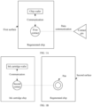
- FIG. 1A is a first schematic diagram of a soldering manner of a regenerated chip in an embodiment of the present invention.
- a chip wafer and a first contact can be disposed on a first surface of the regenerated chip, the chip wafer is connected and in communication with the first contact, and the first contact is in communication with a contact pin for data. It is understood that the chip wafer of the regenerated chip can be disposed on either surface of the regenerated chip.
- FIG. 1B is a second schematic diagram of a soldering manner of a regenerated chip in an embodiment of the present invention.
- the ink cartridge chip is provided with an ink cartridge wafer and a second contact, and the ink cartridge wafer is connected and in communication with the second contact.
- a pad can be disposed on a second surface of the regenerated chip, and a solder joint on the pad can be melted, enabling the solder joint to be electrically connected to the corresponding second contact.
- FIG. 1C is a schematic diagram of a circuit principle of a regenerated chip in the related art.
- the regenerated chip can include a first storage module, which is connected to a printer by a first data signal wire, and the ink cartridge chip is directly disconnected from the printer in a data signal connection, so that the printer can only read storage data of the regenerated chip. Since a data signal sent from the printer by the first data signal wire is not only configured to read the storage data, but also configured to realize functions such as spray point control, the direct disconnection between the ink cartridge chip and the printer will result in the absence of some control functions of the printer and poor printing quality.
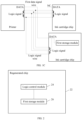
- FIG. 2 is a first block diagram of a structure of the regenerated chip in an embodiment of the present invention.
- the regenerated chip 22 can include a logic control module 24 and a first storage module 26, and the first storage module 26 can include at least one memory.
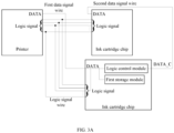
- FIG. 3A is a first schematic diagram of a control circuit principle of a regenerated chip in an embodiment of the present invention.
- the logic control module 24 is electrically connected to a DATA port of the ink cartridge chip by a second data signal wire, and the logic control module 24 is configured to control turn-on or turn-off of the second data signal wire.
- Both the first storage module 26 and the logic control module 24 are electrically connected to a DATA port of the printer by a first data signal wire.
- the control circuit of the regenerated chip can also include other connection.
- FIG. 3B is a second schematic diagram of a control circuit principle of a regenerated chip in an embodiment of the present invention. As shown in FIG.
- the logic control module 24 is connected to the printer by the first data signal line and the logic signal line respectively, the first storage module 26 is connected to the logic control module 24, then the printer can first send a signal to the logic control module 24, and then the logic control module 24 can send the signal to the first storage module 26.
- the first storage module 26 is configured to feed back storage data to the printer by means of the first data signal wire when the second data signal wire is turned off. Therefore, a storage data reading signal of the printer, i.e., a DATA signal, can first enter the regenerated chip 22 by the first data signal wire, and a DATA_C signal processed by the regenerated chip 22 can be transmitted to the ink cartridge chip by the second data signal line.
- a storage data reading signal of the printer i.e., a DATA signal
- a DATA_C signal processed by the regenerated chip 22 can be transmitted to the ink cartridge chip by the second data signal line.
- the first data signal wire connected to the DATA port of the printer can complete a selection function of an address in the first storage module 26 by a digital gate circuit, a shift register and other circuits. By determining a logical combination of signal of a selected address of the first storage module 26, it can determine whether a command sent by the printer has selected the address of a storage unit in the first storage module 26.
- the regenerated chip can only be used when the printer is directly disconnected to the ink cartridge chip in data connection, resulting in poor printing quality.
- the logic control module 24 is disposed in the regenerated chip 22.
- the logic control module 24 is configured to judge a time to turn the first data signal wire on and thus be able to control the spray point, and judge a time to turn the first data signal wire off and thus feed back the storage data to the printer.
- a judgment of the logic control module 24 enables adaptive and accurate control of communication between the printer and the ink cartridge chip, thus replacing storage data in the ink cartridge chip by the storage data in the regenerated chip without affecting transmission of a printing command of the printer, and solving a problem of poor printing quality of the printer with the regenerated chip 22.
- FIG. 4 is a second block diagram of a structure of the regenerated chip in an embodiment of the present invention. As shown in FIG. 4 , the regenerated chip can be applied in a circuit diagram of FIG. 3A and FIG. 3B .
- the logic control module 24 can include a command analysis unit 42 configured for detecting whether an operation command sent by the printer is configured to select the storage unit. The logic control module 24 is configured to control the second data signal wire to be turned off when a selected operation command is detected.
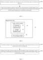
- FIG. 5 is a first flowchart diagram of the method for controlling the regenerated chip in an embodiment of the present invention. As shown in FIG. 5 , the method can be applied to the regenerated chip of FIG. 4 . The method can include the following steps:
- Step 502 detecting an operation command sent by the printer by means of the first data signal wire and the logic signal wire.
- each of a group of section signals, a group of row signals, and a group of column signals in the operation command is expressed as at least one high level
- the selected operation command is configured to indicate that the printer has selected the storage unit in the first storage module 26.
- necessary conditions for selecting the storage unit include: in three groups of section signals, row signals and column signals of an address register of the storage module, (1) a high level must being expressed for section selection; (2) a high level must being expressed for row selection; and (3) a high level must being expressed for column selection. After the above three conditions (1)-(3) are satisfied, it is considered that the command sent by the printer is an operation of selecting the address of the storage unit of the first storage module 26.
- a logical "or” operation can be performed on all section selected signals, all row selected signals, all column selected signals respectively, determining whether a high level is expressed in the three group of section signals, row signals and column signals; then, a logical "and” operation is performed on three signals generated after the above logical "or” operation; finally, a result is detected and analyzed, when the result after the logical "and” operation is 1, the received command is considered to be the selected operation command to select the storage unit, and when the result after the logical "and” operation is 0, the received command is not considered to be the selected operation command.
- the above steps can detect and judge whether the above conditions are met by the logical "or” operation and the logical "and” operation. Only a gate circuit is required in the circuit, so the circuit has a simple structure.
- Step 504 when it is detected that the operation command is not a selected operation command, sending a data signal to the ink cartridge chip by means of the second data signal wire, the data signal being configured to instruct the ink cartridge chip to communicate with the printer.
- a communication between the ink cartridge chip and the printer can include a communication for spray point control or a communication for inkjet time transmission.
- the regenerated chip 22 can transmit signal of the spray point control of the printer to the ink cartridge chip, which in turn enables the printer to accurately control the spray point of the ink cartridge chip.
- each of the group of section signals, the group of row signals, and the group of column signals in the operation command is expressed as at least one high level, and the result after the logical "or" operation and the logical "and” operation is 1, it is determined that the operation command is the selected operation command, i.e., the printer has selected the storage unit in the first storage module 26, and is ready to read the storage data.
- the operation command is not the selected operation command, i.e., the printer does not select the storage unit.
- the second data signal wire when it is detected that the operation command is the selected operation command, the second data signal wire is controlled to be turned off and feed back storage data to the printer by means of the first data signal wire. Since the second data signal wire is controlled to be turned off by the logic control module 24 in the embodiment of the present invention, i.e., the communication between the ink cartridge chip and the printer is stopped, and the printer can only read the storage data in the regenerated chip 22, thus realizing use of the regenerated chip 22 effectively.
- step 502 to step 504 when the regenerated chip 22 receives the operation command of the printer, the operation command is detected and analyzed.
- the second data signal wire is controlled to be turned on.
- the communication between the DATA signal and the original ink cartridge can be opened or stopped selectively based on the analysis and the judgment of the logic control module 24 to the command sent by the printer, implementing automatic control of opening and stopping communication between the printer and the ink cartridge chip according to the command, and avoiding inaccurate control of the spray point due to the communication being stopped directly.
- FIG. 6 is a third block diagram of a structure of a regenerated chip in an embodiment of the present invention.
- the logic control module 24 can further include a voltage feedback unit 62 configured for detecting a feedback voltage between the first storage module 26 of the regenerated chip 22 and a second storage module of the ink cartridge chip.
- FIG. 7 is a second flowchart diagram of a method for controlling a regenerated chip in an embodiment of the present invention. As shown in FIG. 7 , the method can be applied to the regenerated chip 22 of FIG. 6 . The method can include the following steps:
- Step 702 detecting the feedback voltage between the first storage module 26 of the regenerated chip 22 and a second storage module of the ink cartridge chip.
- a feedback voltage of a memory is a feedback result of the first storage module 26 and the second storage module connected in parallel.
- the feedback result is an original level, which means that the selected storage unit of the first storage module 26 does receive the DATA signal for reading the memory, i.e., the second data signal wire is turned off;
- the feedback result is a high level, which means that no storage operation has been performed in the selected storage unit in the first storage module 26;
- the feedback result is a low level, which means that a storage operation has been performed in the selected storage unit in the first storage module 26.
- Step 704 sending the data signal to the ink cartridge chip when the feedback voltage is greater than or equal to a preset voltage, and controlling the second data signal wire to be turned off when the feedback voltage is less than the preset voltage.
- a reference voltage can be preset as the preset voltage and be stored, for example, the preset voltage can be set to 15V.
- the feedback voltage can be compared with the preset voltage to determine a feedback state of the ink cartridge chip and the regenerated chip 22, and turn-on or turn-off of the second data signal wire can be controlled according to the compared result of the feedback voltage and the preset voltage, so that the regenerated chip 22 can feed back storage data to the printer, ensuring accurate control of the printer to the ink cartridge such as spray point control of the ink cartridge, and solving the problem of poor printing quality of the printer with the regenerated chip 22.
- FIG. 8 is a third flowchart diagram of a method for controlling a regenerated chip in an embodiment of the present invention. As shown in FIG. 8 , the method can be applied to the regenerated chip 22 of FIG. 6 . The method can include the following steps:
- Step 802 when it is detected that the operation command is not the selected operation command or the feedback voltage is greater than or equal to the preset voltage, the printer does not select the address of the storage unit in the first storage module 26, or no data has been stored in the selected storage unit in the first storage module 26. Therefore, the first storage module 26 does not need to send data to the printer, the second data signal wire can be kept turning on, and the regenerated chip 22 can send the data signal of the printer to the ink cartridge chip by the second data signal wire.
- the logic control module 24 can compare the feedback voltage with the preset voltage. When the feedback voltage is greater than or equal to the preset voltage, the logic control module 24 can generate a turn-on sub-signal configured to keep connection between the DATA signal of the printer and the ink cartridge chip, and the turn-on sub-signal can be defined as 0. When it is detected that the operation command is not the selected operation command or the turn-on sub-signal is detected, the data signal can be sent to the ink cartridge chip.
- Step 804 when the selected operation command is detected and the feedback voltage is less than the preset voltage, the printer has selected the address of the storage unit in the first storage module 26, and data has been stored in the selected storage unit of the first storage module 26. Therefore, the first storage module 26 should read data in the first storage module 26, i.e., the second data signal wire can be turned off, and the communication between the printer and the ink cartridge chip is stopped.
- the logic control module 24 when the logic control module 24 detects that the feedback voltage is less than the preset voltage, the logic control module 24 can generate a turn-off sub-signal configured to close the connection between the DATA signal of the printer and the ink cartridge chip, and the turn-off sub-signal can be defined as 1.
- the second data signal wire can be controlled to be turned off.
- the logic control module is disposed in the regenerated chip 22 and configured to analyze the command of the printer and compare the feedback voltage, and the communication between the printer and the ink cartridge chip can be controlled based on an integrated analysis, realizing an isolation of data communication and logic signal transmission for memory reading.
- an analysis of the command of the printer and comparation of the feedback voltage are considered, and it is judged whether the regenerated chip 22 should transit the DATA signal to the ink cartridge based on the integrated analysis, thus improving accuracy of communication control between the printer and the ink cartridge chip.
- FIG. 5, FIG. 7 , and FIG. 8 are shown sequentially as indicated by the arrows, the steps are not necessarily performed sequentially in the order indicated by the arrows. Except as expressly stated herein, there is no strict sequential limitation on the execution of these steps, and the steps may be executed in any other order. Moreover, at least some of the steps in FIG. 5, FIG. 7 , and FIG. 8 may include multiple sub-steps or multiple stages that are not necessarily performed at the same time, but may be performed at different times, and the order in which these sub-steps or stages are performed is not necessarily sequential, but may alternate with other steps or at least some of the sub-steps or stages of other steps.
- FIG. 9 is a fourth block diagram of a structure of a regenerated chip in an embodiment of the present invention.
- the regenerated chip 22 is further provided with a switch circuit 92 connected to the logic control module 24.
- the switch circuit 92 is disposed in a wafer of the regenerated chip 22, or outside the wafer of the regenerated chip 22.
- the logic control module 24 is further configured to control turn-off of the second data signal wire by means of the switch circuit 92.
- the switch circuit 92 can include a triode switch circuit.
- the switch circuit 92 can further include at least one of a switch diode, a logic gate circuit, a bistable trigger or other switch circuit.
- FIG. 10 is a block diagram of a regenerated ink cartridge in an embodiment of the present invention.
- the regenerated ink cartridge 108 is electrically connected to a printer body 102
- the regenerated ink cartridge 108 can include an ink cartridge body 106, an ink cartridge chip 104, and a regenerated chip 22, and the ink cartridge body 106 is connected to the ink cartridge chip 104.
- the regenerated chip 22 can include a logic control module 24 and a first storage module 26.
- the logic control module 24 is electrically connected to the printer body 102 by means of a first data signal wire and a logic signal wire, and electrically connected to the ink cartridge chip 104 by means of a second data signal wire.
- the logic control module 24 is configured to detect a command sent from the printer body 102 by means of the first data signal wire and the logic signal wire, and control the second data signal wire to be turned on or turned off.
- the logic control module 24 is further configured to send a data signal to the ink cartridge chip 104 by means of the second data signal wire.
- the data signal is configured to instruct the ink cartridge chip 104 to communicate with the printer body 102.
- the logic control module 24 is disposed in the regenerated chip 22.
- the logic control module 24 is configured to judge a time to turn the first data signal wire on and thus be able to control the spray point, and judge a time to turn the first data signal wire off and thus feed back the storage data to the printer.
- a judgment of the logic control module 24 enables adaptive and accurate control of communication between the printer and the ink cartridge chip 104, thus replacing storage data in the ink cartridge chip 104 by the storage data in the regenerated chip 22 without affecting transmission of a printing command of the printer body 102, and solving a problem of poor printing quality of the printer with the regenerated chip 22.
Landscapes
- Ink Jet (AREA)
Description
- The present invention relates to the field of a printer, and in particular, to a regenerated chip, a regenerated ink cartridge, and a method for controlling the regenerated chip.
- With increasing awareness of environmental protection and demand for resource recycling, reuse of a regenerated chip of an ink cartridge has been greatly improved, and more and more waste ink cartridges are reused, reducing waste and pollution to the environment.
- In the related art, a data signal wire of a printer can be used to read data stored in a chip of an original ink cartridge, which can be data of a selected storage unit, except when the data stored in the chip of the original ink cartridge is no longer available. Therefore, it is necessary to stop communication through the data signal wire between the printer and the original ink cartridge and directly connect the regenerated chip to the printer through a communication signal wire. As such when the printer reads data of a data storage area of the chip of the original ink cartridge, the DATA signal can only enter a data area of the regenerated chip to read data stored in the regenerated chip.
- However, in the related art, the DATA signal is not only configured to read the data of the data storage area of the chip of the original ink cartridge, but also has other functions, such as a function of a logic signal of controlling selection of a print spot of the ink cartridge. Therefore, stopping a DATA signal communication between the printer and the original ink cartridge would affect other important functions including the selection of the print spot of the ink cartridge when an upgraded printer prints, and affect printing effect, resulting in poor printing quality of the printer with the regenerated chip.
-
CN207669999U discloses a kind of regeneration chip component of printing consumables, including: original-pack chip, compatible chip and the control chip being connect respectively with printer. The control chip is also connected to the original-pack chip and the compatible chip respectively, so that the control chip is controlled according to the enable signal of the printer received, the original-pack chip, the compatible chip is in running order or/reset state of awaiting orders.EP3395577 A1 discloses a repair method and repair chip for a regenerative ink cartridge, and a regenerative ink cartridge. The repair chip does not need to monitor all lines of a printer and only needs to monitor an enable line, a data line and auxiliary lines of the printer, so that the number of pads, electrically connected with the printer, of an original chip is reduced, the welding difficulty and workload in the ink cartridge regeneration process are lowered accordingly, and the risk of ink cartridge scraping in the repair process is lowered from the source. - For the issue of poor printing quality of the printer with the regenerated chip, no effective solution has been proposed so far.
- According to various embodiments of the present invention, a regenerated chip, and a regenerated ink cartridge, and a method for controlling the regenerated chip are provided to solve a problem of poor printing quality of the printer with the regenerated chip in the related art.
- In a first aspect, the present invention provides the method for controlling the regenerated chip. The regenerated chip is electrically connected to a printer by means of a first data signal wire and a logic signal wire, and is electrically connected to an ink cartridge chip by means of a second data signal wire. The method includes: detecting an operation command sent by the printer by means of the first data signal wire and the logic signal wire; and when it is detected that the operation command is not a selected operation command, sending a data signal to the ink cartridge chip by means of the second data signal wire. The data signal is configured to instruct the ink cartridge chip to communicate with the printer.
- In an embodiment of the present invention, after the detecting the operation command sent by the printer, the method further includes: when it is detected that the operation command is the selected operation command, controlling the second data signal wire to be turned off and feeding back storage data to the printer by means of the first data signal wire.
- In an embodiment of the present invention, before the sending the data signal to the ink cartridge chip by means of the second data signal wire, the method further includes: detecting a feedback voltage between a first storage module of the regenerated chip and a second storage module of the ink cartridge chip; sending the data signal to the ink cartridge chip when the feedback voltage is greater than or equal to a preset voltage; and controlling the second data signal wire to be turned off when the feedback voltage is less than the preset voltage. The first storage module and the second storage module are connected in parallel.
- In an embodiment of the present invention, after detecting the feedback voltage between the first storage module of the regenerated chip and the second storage module of the ink cartridge chip, the method further includes: when it is detected that the operation command is not the selected operation command or the feedback voltage is greater than or equal to the preset voltage, sending the data signal to the ink cartridge chip; and when the selected operation command is detected and the feedback voltage is less than the preset voltage, controlling the second data signal wire to be turned off.
- In an embodiment of the present invention, the method further includes: when the feedback voltage is greater than or equal to the preset voltage, generating a turn-on sub-signal; when the feedback voltage is less than the preset voltage, generating a turn-off sub-signal; when it is detected that the operation command is not the selected operation command or the turn-on sub-signal is detected, sending the data signal to the ink cartridge chip; and when both the selected operation command and the turn-off sub-signal are detected, controlling the second data signal wire to be turned off.
- In an embodiment of the present invention, detecting that the operation command sent by the printer is not the selected operation command includes: when it is detected that each of a group of section signals, a group of row signals, and a group of column signals in the operation command is expressed as at least one high level, determining that the operation command is the selected operation command; and when it is detected that at least one of the group of section signals, the group of row signals, and the group of column signals is not expressed as high level, determining that the operation command is not the selected operation command.
- In an embodiment of the present invention, a communication between the ink cartridge chip and the printer includes a communication for spray point control or a communication for inkjet time transmission.
- In an embodiment of the present invention, the method further includes controlling turn-on or turn-off of the second data signal wire by means of a switch circuit. The switch circuit is disposed in a wafer of the regenerated chip, or outside the wafer of the regenerated chip.
- In an embodiment of the present invention, the switch circuit comprises at least one of a triode switch circuit, a switch diode, a logic gate circuit, or a bistable trigger.
- In a second aspect, the present invention provides the regenerated chip which is applied to the regenerated ink cartridge. The regenerated chip includes a logic control module and a first storage module. The logic control module is electrically connected to a printer by means of a first data signal wire and a logic signal wire, and is electrically connected to an ink cartridge chip by means of a second data signal wire. The logic control module includes a command analysis unit configured for detecting an operation command sent by the printer by means of the first data signal wire and the logic signal wire. The logic control module is configured for sending a data signal to the ink cartridge chip by means of the second data signal wire when it is detected that the operation command is not a selected operation command. The data signal is configured to instruct the ink cartridge chip to communicate with the printer. The logic control module is further configured for controlling the second data signal wire to be turned off when it is detected that the operation command is the selected operation command, and the first storage module is configured for feeding back storage data to the printer by means of the first data signal wire.
- In an embodiment of the present invention, the logic control module further includes a voltage feedback unit. The voltage feedback unit is configured for detecting a feedback voltage between the first storage module of the regenerated chip and a second storage module of the ink cartridge chip, and the first storage module and the second storage module are connected in parallel. The logic control module is further configured for sending the data signal to the ink cartridge chip when the feedback voltage is detected to be greater than or equal to a preset voltage. The logic control module is further configured for controlling the second data signal wire to be turned off when the feedback voltage is detected to be less than the preset voltage.
- In an embodiment of the present invention, the regenerated chip is provided with a switch circuit, the switch circuit is connected to the logic control module, and the switch circuit is disposed in the regenerated chip or outside a wafer of the regenerated chip. The logic control module is further configured for controlling turn-on or turn-off of the second data signal wire by means of the switch circuit.
- In a third aspect, the present invention provides a regenerated ink cartridge. The regenerated ink cartridge includes an ink cartridge body, an ink cartridge chip and a regenerated chip. The ink cartridge body is connected to the ink cartridge chip, and the regenerated chip is configured for implementing the method as described in the first aspect above.
- In contrast to the related art, the present invention provides the method for controlling the regenerated chip, the regenerated chip, and the regenerated ink cartridge. The regenerated chip is electrically connected to the printer by means of the first data signal wire and the logic signal wire, and is electrically connected to the ink cartridge chip by means of the second data signal wire. The operation command sent by the printer through the first data signal wire is detected by the first data signal wire and the logic signal wire. When it is detected that the operation command is not the selected operation command, the data signal is sent to the ink cartridge chip by means of the second data signal wire. The data signal is configured to instruct the ink cartridge chip to communicate with the printer, solving the problem of poor printing quality of the printer with the regenerated chip.
- Details of one or more embodiments of the present invention are presented in the following accompanying drawings and description to enable other features, purposes and advantages of the present invention more concise and understandable.
- In order to better describe and explain the embodiments and/or examples of those inventions disclosed herein, one or more drawings may be referred to. The additional details or examples used to describe the drawings should not be considered as limiting the scope of any of the disclosed inventions, the currently described embodiments and/or examples, and the best mode of these inventions currently understood.
-
FIG. 1A is a first schematic diagram of a soldering manner of a regenerated chip in an embodiment of the present invention. -
FIG. 1B is a second schematic diagram of a soldering manner of a regenerated chip in an embodiment of the present invention. -
FIG. 1C is a schematic diagram of a circuit principle of a regenerated chip in the related art. -
FIG. 2 is a first block diagram of a structure of a regenerated chip in an embodiment of the present invention. -
FIG. 3A is a first schematic diagram of a control circuit principle of a regenerated chip in an embodiment of the present invention. -
FIG. 3B is a second schematic diagram of a control circuit principle of a regenerated chip in an embodiment of the present invention. -
FIG. 4 is a second block diagram of a structure of a regenerated chip in an embodiment of the present invention. -
FIG. 5 is a first flowchart diagram of a method for controlling a regenerated chip in an embodiment of the present invention. -
FIG. 6 is a third block diagram of a structure of a regenerated chip in an embodiment of the present invention. -
FIG. 7 is a second flowchart diagram of a method for controlling a regenerated chip in an embodiment of the present invention. -
FIG. 8 is a third flowchart diagram of a method for controlling a regenerated chip in an embodiment of the present invention. -
FIG. 9 is a fourth block diagram of a structure of a regenerated chip in an embodiment of the present invention. -
FIG. 10 is a block diagram of a regenerated ink cartridge in an embodiment of the present invention. - In the figures, 22 represents a regenerated chip; 24 represents a logic control module; 26 represents a first storage module; 42 represents a command analysis unit; 62 represents a voltage feedback unit; 92 represents a switch circuit; 102 represents a printer body; 104 represents an ink cartridge chip; 106 represents an ink cartridge body; and 108 represents a regenerated ink cartridge.
- In order to make the purpose, technical solutions and advantages of the present invention clearer and more understood, the present invention will be described and illustrated below with reference to the accompanying drawings and embodiments. The described embodiments herein are intended to explain the present invention only and are not intended to limit the present invention. Based on the embodiments of the present invention, all other embodiments obtained by one skilled in the art without creative efforts all belong to the scope of protection of the present invention, which is defined by the appended claims.
- It is apparent that the accompanying drawings in the following description are only some examples or embodiments of the present invention, and that the present invention may be applied to other similar scenarios in accordance with these drawings without creative efforts by one skilled in the art. It is also understood that, although the efforts made in such development process may complex and lengthy, some changes of design, manufacturing or production based on the technical content disclosed in the present invention are only conventional technical means for one skilled in the art related to the content disclosed in the present invention, and should not be construed that the content disclosed in the present invention is inadequate.
- References to "embodiment" in the present invention mean that a particular feature, a structure, or a characteristic described in conjunction with an embodiment may be included in at least one embodiment of the present invention. The occurrence of the "embodiment" at various positions in the description does not necessarily mean the same embodiment, nor is it a separate or alternative embodiment that is mutually exclusive with other embodiments. It is understood, both explicitly and implicitly, by one skilled in the art that the embodiment described in the present invention may be combined with other embodiments without conflict.
- Unless otherwise defined, all technical and scientific terms used herein have the same meaning as a skilled person in the art would understand. The term "one", "a", "an", "the" and other similar words as used in the present invention do not indicate quantitative limitations, and they can be singular or plural. The terms "include", "comprise", "have", and any variation thereof, as used in the present invention, are intended to cover a non-exclusive inclusion. For example, processes, methods, systems, products or devices including a series of steps or modules (units) are not limited to listed steps or modules (units), but may include steps or modules (units) not listed, or may include other steps or modules (units) inherent in those processes, methods, systems, products or devices. The terms "connection", "connected", "coupling", and other similar words as used in the present invention are not limited to physical or mechanical connections, but may include electrical connections, which can be direct connections or indirect connections. The term "plurality" in the present invention refers to two or more. "And/or" describes an association relationship between associated objects, indicating that there can be three kinds of relationships. For example, "A and/or B" can mean that A exists alone, A and B exist at the same time, and B exists alone. Normally, the character "/" indicates that the objects associated with each other are in an "or" relationship. The terms "first", "second", "third", etc. involved in the present invention are only configured for distinguishing similar objects, and do not represent a specific order of the objects.
- In an embodiment, a regenerated chip is provided which is applied to a regenerated ink cartridge and covering on an ink cartridge chip of the regenerated ink cartridge.
FIG. 1A is a first schematic diagram of a soldering manner of a regenerated chip in an embodiment of the present invention. As shown inFIG. 1A , a chip wafer and a first contact can be disposed on a first surface of the regenerated chip, the chip wafer is connected and in communication with the first contact, and the first contact is in communication with a contact pin for data. It is understood that the chip wafer of the regenerated chip can be disposed on either surface of the regenerated chip. -
FIG. 1B is a second schematic diagram of a soldering manner of a regenerated chip in an embodiment of the present invention. As shown inFIG. 1B , the ink cartridge chip is provided with an ink cartridge wafer and a second contact, and the ink cartridge wafer is connected and in communication with the second contact. A pad can be disposed on a second surface of the regenerated chip, and a solder joint on the pad can be melted, enabling the solder joint to be electrically connected to the corresponding second contact. -
FIG. 1C is a schematic diagram of a circuit principle of a regenerated chip in the related art. As shown inFIG. 1C , the regenerated chip can include a first storage module, which is connected to a printer by a first data signal wire, and the ink cartridge chip is directly disconnected from the printer in a data signal connection, so that the printer can only read storage data of the regenerated chip. Since a data signal sent from the printer by the first data signal wire is not only configured to read the storage data, but also configured to realize functions such as spray point control, the direct disconnection between the ink cartridge chip and the printer will result in the absence of some control functions of the printer and poor printing quality. - In an embodiment, a regenerated
chip 22 is provided.FIG. 2 is a first block diagram of a structure of the regenerated chip in an embodiment of the present invention. As shown inFIG. 2 , the regeneratedchip 22 can include alogic control module 24 and afirst storage module 26, and thefirst storage module 26 can include at least one memory. -
FIG. 3A is a first schematic diagram of a control circuit principle of a regenerated chip in an embodiment of the present invention. As shown inFIG. 3A , thelogic control module 24 is electrically connected to a DATA port of the ink cartridge chip by a second data signal wire, and thelogic control module 24 is configured to control turn-on or turn-off of the second data signal wire. Both thefirst storage module 26 and thelogic control module 24 are electrically connected to a DATA port of the printer by a first data signal wire. It can be understood that the control circuit of the regenerated chip can also include other connection. For example,FIG. 3B is a second schematic diagram of a control circuit principle of a regenerated chip in an embodiment of the present invention. As shown inFIG. 3B , thelogic control module 24 is connected to the printer by the first data signal line and the logic signal line respectively, thefirst storage module 26 is connected to thelogic control module 24, then the printer can first send a signal to thelogic control module 24, and then thelogic control module 24 can send the signal to thefirst storage module 26. - The
first storage module 26 is configured to feed back storage data to the printer by means of the first data signal wire when the second data signal wire is turned off. Therefore, a storage data reading signal of the printer, i.e., a DATA signal, can first enter the regeneratedchip 22 by the first data signal wire, and a DATA_C signal processed by the regeneratedchip 22 can be transmitted to the ink cartridge chip by the second data signal line. - The first data signal wire connected to the DATA port of the printer can complete a selection function of an address in the
first storage module 26 by a digital gate circuit, a shift register and other circuits. By determining a logical combination of signal of a selected address of thefirst storage module 26, it can determine whether a command sent by the printer has selected the address of a storage unit in thefirst storage module 26. - In the related art, the regenerated chip can only be used when the printer is directly disconnected to the ink cartridge chip in data connection, resulting in poor printing quality. In the above embodiment of the present invention, the
logic control module 24 is disposed in the regeneratedchip 22. Thelogic control module 24 is configured to judge a time to turn the first data signal wire on and thus be able to control the spray point, and judge a time to turn the first data signal wire off and thus feed back the storage data to the printer. A judgment of thelogic control module 24 enables adaptive and accurate control of communication between the printer and the ink cartridge chip, thus replacing storage data in the ink cartridge chip by the storage data in the regenerated chip without affecting transmission of a printing command of the printer, and solving a problem of poor printing quality of the printer with the regeneratedchip 22. - In an embodiment, a regenerated chip is provided.
FIG. 4 is a second block diagram of a structure of the regenerated chip in an embodiment of the present invention. As shown inFIG. 4 , the regenerated chip can be applied in a circuit diagram ofFIG. 3A andFIG. 3B . Thelogic control module 24 can include acommand analysis unit 42 configured for detecting whether an operation command sent by the printer is configured to select the storage unit. Thelogic control module 24 is configured to control the second data signal wire to be turned off when a selected operation command is detected. - A method for controlling a regenerated chip is further provided in an embodiment.
FIG. 5 is a first flowchart diagram of the method for controlling the regenerated chip in an embodiment of the present invention. As shown inFIG. 5 , the method can be applied to the regenerated chip ofFIG. 4 . The method can include the following steps: -
Step 502, detecting an operation command sent by the printer by means of the first data signal wire and the logic signal wire. - In some embodiments, when it is detected that each of a group of section signals, a group of row signals, and a group of column signals in the operation command is expressed as at least one high level, it is determined that the operation command is the selected operation command. The selected operation command is configured to indicate that the printer has selected the storage unit in the
first storage module 26. - It should be noted that necessary conditions for selecting the storage unit include: in three groups of section signals, row signals and column signals of an address register of the storage module, (1) a high level must being expressed for section selection; (2) a high level must being expressed for row selection; and (3) a high level must being expressed for column selection. After the above three conditions (1)-(3) are satisfied, it is considered that the command sent by the printer is an operation of selecting the address of the storage unit of the
first storage module 26. - It can be judged whether the above conditions are met by the following steps: firstly, a logical "or" operation can be performed on all section selected signals, all row selected signals, all column selected signals respectively, determining whether a high level is expressed in the three group of section signals, row signals and column signals; then, a logical "and" operation is performed on three signals generated after the above logical "or" operation; finally, a result is detected and analyzed, when the result after the logical "and" operation is 1, the received command is considered to be the selected operation command to select the storage unit, and when the result after the logical "and" operation is 0, the received command is not considered to be the selected operation command. The above steps can detect and judge whether the above conditions are met by the logical "or" operation and the logical "and" operation. Only a gate circuit is required in the circuit, so the circuit has a simple structure.
- Step 504, when it is detected that the operation command is not a selected operation command, sending a data signal to the ink cartridge chip by means of the second data signal wire, the data signal being configured to instruct the ink cartridge chip to communicate with the printer.
- In some embodiments, a communication between the ink cartridge chip and the printer can include a communication for spray point control or a communication for inkjet time transmission. For example, when the selected operation command is not detected, the regenerated
chip 22 can transmit signal of the spray point control of the printer to the ink cartridge chip, which in turn enables the printer to accurately control the spray point of the ink cartridge chip. - In some embodiments, when it is detected that each of the group of section signals, the group of row signals, and the group of column signals in the operation command is expressed as at least one high level, and the result after the logical "or" operation and the logical "and" operation is 1, it is determined that the operation command is the selected operation command, i.e., the printer has selected the storage unit in the
first storage module 26, and is ready to read the storage data. When it is detected that at least one of the group of section signals, the group of row signals, and the group of column signals is not expressed as high level, and the result after the logical "or" operation and the logical "and" operation is 0, it is determined that the operation command is not the selected operation command, i.e., the printer does not select the storage unit. - In some embodiments, when it is detected that the operation command is the selected operation command, the second data signal wire is controlled to be turned off and feed back storage data to the printer by means of the first data signal wire. Since the second data signal wire is controlled to be turned off by the
logic control module 24 in the embodiment of the present invention, i.e., the communication between the ink cartridge chip and the printer is stopped, and the printer can only read the storage data in the regeneratedchip 22, thus realizing use of the regeneratedchip 22 effectively. - In the
above step 502 to step 504, when the regeneratedchip 22 receives the operation command of the printer, the operation command is detected and analyzed. When it is detected that the printer does not select the address of the storage unit of thefirst storage module 26, the second data signal wire is controlled to be turned on. Thus, the communication between the DATA signal and the original ink cartridge can be opened or stopped selectively based on the analysis and the judgment of thelogic control module 24 to the command sent by the printer, implementing automatic control of opening and stopping communication between the printer and the ink cartridge chip according to the command, and avoiding inaccurate control of the spray point due to the communication being stopped directly. - In some embodiments, a regenerated chip is provided.
FIG. 6 is a third block diagram of a structure of a regenerated chip in an embodiment of the present invention. As shown inFIG. 6 , thelogic control module 24 can further include avoltage feedback unit 62 configured for detecting a feedback voltage between thefirst storage module 26 of the regeneratedchip 22 and a second storage module of the ink cartridge chip. - A method for controlling a regenerated chip is further provided in an embodiment.
FIG. 7 is a second flowchart diagram of a method for controlling a regenerated chip in an embodiment of the present invention. As shown inFIG. 7 , the method can be applied to the regeneratedchip 22 ofFIG. 6 . The method can include the following steps: -
Step 702, detecting the feedback voltage between thefirst storage module 26 of the regeneratedchip 22 and a second storage module of the ink cartridge chip. - It should be noted that the printer can read storage data in the regenerated
chip 22 and the ink cartridge chip initially. A feedback voltage of a memory is a feedback result of thefirst storage module 26 and the second storage module connected in parallel. There are the following three feedback results: (1) the feedback result is an original level, which means that the selected storage unit of thefirst storage module 26 does receive the DATA signal for reading the memory, i.e., the second data signal wire is turned off; (2) the feedback result is a high level, which means that no storage operation has been performed in the selected storage unit in thefirst storage module 26; (3) the feedback result is a low level, which means that a storage operation has been performed in the selected storage unit in thefirst storage module 26. -
Step 704, sending the data signal to the ink cartridge chip when the feedback voltage is greater than or equal to a preset voltage, and controlling the second data signal wire to be turned off when the feedback voltage is less than the preset voltage. - A reference voltage can be preset as the preset voltage and be stored, for example, the preset voltage can be set to 15V.
- In the
above step 702 to step 704, the feedback voltage can be compared with the preset voltage to determine a feedback state of the ink cartridge chip and the regeneratedchip 22, and turn-on or turn-off of the second data signal wire can be controlled according to the compared result of the feedback voltage and the preset voltage, so that the regeneratedchip 22 can feed back storage data to the printer, ensuring accurate control of the printer to the ink cartridge such as spray point control of the ink cartridge, and solving the problem of poor printing quality of the printer with the regeneratedchip 22. - In some embodiments, a method for controlling a regenerated chip is further provided.
FIG. 8 is a third flowchart diagram of a method for controlling a regenerated chip in an embodiment of the present invention. As shown inFIG. 8 , the method can be applied to the regeneratedchip 22 ofFIG. 6 . The method can include the following steps: - Step 802, when it is detected that the operation command is not the selected operation command or the feedback voltage is greater than or equal to the preset voltage, the printer does not select the address of the storage unit in the
first storage module 26, or no data has been stored in the selected storage unit in thefirst storage module 26. Therefore, thefirst storage module 26 does not need to send data to the printer, the second data signal wire can be kept turning on, and the regeneratedchip 22 can send the data signal of the printer to the ink cartridge chip by the second data signal wire. - In some embodiments, the
logic control module 24 can compare the feedback voltage with the preset voltage. When the feedback voltage is greater than or equal to the preset voltage, thelogic control module 24 can generate a turn-on sub-signal configured to keep connection between the DATA signal of the printer and the ink cartridge chip, and the turn-on sub-signal can be defined as 0. When it is detected that the operation command is not the selected operation command or the turn-on sub-signal is detected, the data signal can be sent to the ink cartridge chip. - Step 804, when the selected operation command is detected and the feedback voltage is less than the preset voltage, the printer has selected the address of the storage unit in the
first storage module 26, and data has been stored in the selected storage unit of thefirst storage module 26. Therefore, thefirst storage module 26 should read data in thefirst storage module 26, i.e., the second data signal wire can be turned off, and the communication between the printer and the ink cartridge chip is stopped. - In some embodiments, when the
logic control module 24 detects that the feedback voltage is less than the preset voltage, thelogic control module 24 can generate a turn-off sub-signal configured to close the connection between the DATA signal of the printer and the ink cartridge chip, and the turn-off sub-signal can be defined as 1. When the selected operation command and the turn-off sub-signal are detected, the second data signal wire can be controlled to be turned off. - In the above step 802 to step 804, the logic control module is disposed in the regenerated
chip 22 and configured to analyze the command of the printer and compare the feedback voltage, and the communication between the printer and the ink cartridge chip can be controlled based on an integrated analysis, realizing an isolation of data communication and logic signal transmission for memory reading. At the same time, an analysis of the command of the printer and comparation of the feedback voltage are considered, and it is judged whether the regeneratedchip 22 should transit the DATA signal to the ink cartridge based on the integrated analysis, thus improving accuracy of communication control between the printer and the ink cartridge chip. - Although individual steps in the flowchart diagrams of
FIG. 5, FIG. 7 , andFIG. 8 are shown sequentially as indicated by the arrows, the steps are not necessarily performed sequentially in the order indicated by the arrows. Except as expressly stated herein, there is no strict sequential limitation on the execution of these steps, and the steps may be executed in any other order. Moreover, at least some of the steps inFIG. 5, FIG. 7 , andFIG. 8 may include multiple sub-steps or multiple stages that are not necessarily performed at the same time, but may be performed at different times, and the order in which these sub-steps or stages are performed is not necessarily sequential, but may alternate with other steps or at least some of the sub-steps or stages of other steps. - In some embodiments, a regenerated chip and a method for controlling the same are provided.
FIG. 9 is a fourth block diagram of a structure of a regenerated chip in an embodiment of the present invention. As shown inFIG. 9 , the regeneratedchip 22 is further provided with aswitch circuit 92 connected to thelogic control module 24. Theswitch circuit 92 is disposed in a wafer of the regeneratedchip 22, or outside the wafer of the regeneratedchip 22. Thelogic control module 24 is further configured to control turn-off of the second data signal wire by means of theswitch circuit 92. Theswitch circuit 92 can include a triode switch circuit. When thelogic control module 24 transmits a high level signal according to the judgment, the triode switch circuit can be closed, enabling the second data signal wire to be turned off. Theswitch circuit 92 can further include at least one of a switch diode, a logic gate circuit, a bistable trigger or other switch circuit. - In some embodiments, a regenerated ink cartridge is provided.
FIG. 10 is a block diagram of a regenerated ink cartridge in an embodiment of the present invention. As shown inFIG. 10 , the regeneratedink cartridge 108 is electrically connected to aprinter body 102, the regeneratedink cartridge 108 can include anink cartridge body 106, anink cartridge chip 104, and a regeneratedchip 22, and theink cartridge body 106 is connected to theink cartridge chip 104. - The regenerated
chip 22 can include alogic control module 24 and afirst storage module 26. Thelogic control module 24 is electrically connected to theprinter body 102 by means of a first data signal wire and a logic signal wire, and electrically connected to theink cartridge chip 104 by means of a second data signal wire. Thelogic control module 24 is configured to detect a command sent from theprinter body 102 by means of the first data signal wire and the logic signal wire, and control the second data signal wire to be turned on or turned off. Thelogic control module 24 is further configured to send a data signal to theink cartridge chip 104 by means of the second data signal wire. The data signal is configured to instruct theink cartridge chip 104 to communicate with theprinter body 102. - In the above embodiments, the
logic control module 24 is disposed in the regeneratedchip 22. Thelogic control module 24 is configured to judge a time to turn the first data signal wire on and thus be able to control the spray point, and judge a time to turn the first data signal wire off and thus feed back the storage data to the printer. A judgment of thelogic control module 24 enables adaptive and accurate control of communication between the printer and theink cartridge chip 104, thus replacing storage data in theink cartridge chip 104 by the storage data in the regeneratedchip 22 without affecting transmission of a printing command of theprinter body 102, and solving a problem of poor printing quality of the printer with the regeneratedchip 22.
Claims (11)
- A method for controlling a regenerated chip (22), wherein the regenerated chip (22) is electrically connected to a printer by means of a first data signal wire and a logic signal wire, and is electrically connected to an ink cartridge chip (104) by means of a second data signal wire, and the method comprises:detecting an operation command sent by the printer by means of the first data signal wire and the logic signal wire; andwhen it is detected that the operation command is not a selected operation command, sending a data signal to the ink cartridge chip (104) by means of the second data signal wire, wherein the data signal is configured to instruct the ink cartridge chip (104) to communicate with the printer;before the sending the data signal to the ink cartridge chip (104) by means of the second data signal wire, the method further comprises:detecting a feedback voltage between a first storage module (26) of the regenerated chip (22) and a second storage module of the ink cartridge chip (104), wherein the first storage module (26) and the second storage module are connected in parallel;sending the data signal to the ink cartridge chip (104) when the feedback voltage is greater than or equal to a preset voltage; andcontrolling the second data signal wire to be turned off when the feedback voltage is less than the preset voltage.
- The method of claim 1, characterized in that after the detecting the operation command sent by the printer, the method further comprises:
when it is detected that the operation command is the selected operation command, controlling the second data signal wire to be turned off and feeding back storage data to the printer by means of the first data signal wire. - The method of claim 1, characterized in that after detecting the feedback voltage between the first storage module (26) of the regenerated chip (22) and the second storage module of the ink cartridge chip (104), the method further comprises:when it is detected that the operation command is not the selected operation command or the feedback voltage is greater than or equal to the preset voltage, sending the data signal to the ink cartridge chip (104); andwhen the selected operation command is detected and the feedback voltage is less than the preset voltage, controlling the second data signal wire to be turned off.
- The method of claim 3, characterized by further comprising:when the feedback voltage is greater than or equal to the preset voltage, generating a turn-on sub-signal;when the feedback voltage is less than the preset voltage, generating a turn-off sub-signal;when it is detected that the operation command is not the selected operation command or the turn-on sub-signal is detected, sending the data signal to the ink cartridge chip (104); andwhen both the selected operation command and the turn-off sub-signal are detected, controlling the second data signal wire to be turned off.
- The method of claim 4, characterized in that detecting that the operation command sent by the printer is not the selected operation command comprises:when it is detected that each of a group of section signals, a group of row signals, and a group of column signals in the operation command is expressed as at least one high level, determining that the operation command is the selected operation command; andwhen it is detected that at least one of the group of section signals, the group of row signals, and the group of column signals is not expressed as high level, determining that the operation command is not the selected operation command.
- The method of any one of claims 1 to 5, characterized in that a communication between the ink cartridge chip (104) and the printer comprises a communication for spray point control or a communication for inkjet time transmission.
- The method of any one of claims 1 to 5, characterized by further comprising:controlling turn-on or turn-off of the second data signal wire by means of a switch circuit (92);wherein the switch circuit (92) is disposed in a wafer of the regenerated chip (22), or outside the wafer of the regenerated chip (22).
- The method of claim 7, characterized in that the switch circuit (92) comprises at least one of a triode switch circuit, a switch diode, a logic gate circuit, or a bistable trigger.
- A regenerated chip (22) applied to a regenerated ink cartridge (108), whereinthe regenerated chip (22) comprises a logic control module (24) and a first storage module (26);the logic control module (24) is electrically connected to a printer by means of a first data signal wire and a logic signal wire, and is electrically connected to an ink cartridge chip (104) by means of a second data signal wire;the logic control module (24) comprises a command analysis unit (42) configured for detecting an operation command sent by the printer by means of the first data signal wire and the logic signal wire;the logic control module (24) is configured for sending a data signal to the ink cartridge chip (104) by means of the second data signal wire when it is detected that the operation command is not a selected operation command, wherein the data signal is configured to instruct the ink cartridge chip (104) to communicate with the printer; andthe logic control module (24) is further configured for controlling the second data signal wire to be turned off when it is detected that the operation command is the selected operation command, and the first storage module (26) is configured for feeding back storage data to the printer by means of the first data signal wire;the logic control module (24) further comprises a voltage feedback unit (62);the voltage feedback unit (62) is configured for detecting a feedback voltage between the first storage module (26) of the regenerated chip (22) and a second storage module of the ink cartridge chip (104), wherein the first storage module (26) and the second storage module are connected in parallel;the logic control module (24) is further configured for sending the data signal to the ink cartridge chip (104) when the feedback voltage is detected to be greater than or equal to a preset voltage; andthe logic control module (24) is further configured for controlling the second data signal wire to be turned off when the feedback voltage is detected to be less than the preset voltage.
- The regenerated chip (22) of claim 9, characterized in that the regenerated chip (22) is provided with a switch circuit (92), the switch circuit (92) is connected to the logic control module (24), and the switch circuit (92) is disposed in the regenerated chip (22) or outside a wafer of the regenerated chip (22); and
the logic control module (24) is further configured for controlling turn-on or turn-off of the second data signal wire by means of the switch circuit (92). - A regenerated ink cartridge (108), wherein the regenerated ink cartridge (108) comprises an ink cartridge body (106), an ink cartridge chip (104) and a regenerated chip (22),
the ink cartridge body (106) is connected to the ink cartridge chip (104), and the regenerated chip (22) is configured for implementing the method of any one of claims 1 to 8.
Applications Claiming Priority (2)
| Application Number | Priority Date | Filing Date | Title |
|---|---|---|---|
| CN202010528226.4A CN111746133B (en) | 2020-06-11 | 2020-06-11 | Control method of regeneration chip, regeneration chip and regeneration ink box |
| PCT/CN2021/085243 WO2021248990A1 (en) | 2020-06-11 | 2021-04-02 | Method for controlling regenerated chip, regenerated chip and regenerated ink cartridge |
Publications (3)
| Publication Number | Publication Date |
|---|---|
| EP4112315A1 EP4112315A1 (en) | 2023-01-04 |
| EP4112315A4 EP4112315A4 (en) | 2023-08-09 |
| EP4112315B1 true EP4112315B1 (en) | 2025-05-28 |
Family
ID=72675085
Family Applications (1)
| Application Number | Title | Priority Date | Filing Date |
|---|---|---|---|
| EP21822814.6A Active EP4112315B1 (en) | 2020-06-11 | 2021-04-02 | Method for controlling regenerated chip, regenerated chip and regenerated ink cartridge |
Country Status (4)
| Country | Link |
|---|---|
| US (1) | US12128687B2 (en) |
| EP (1) | EP4112315B1 (en) |
| CN (1) | CN111746133B (en) |
| WO (1) | WO2021248990A1 (en) |
Families Citing this family (6)
| Publication number | Priority date | Publication date | Assignee | Title |
|---|---|---|---|---|
| CN111746133B (en) | 2020-06-11 | 2021-11-16 | 杭州旗捷科技有限公司 | Control method of regeneration chip, regeneration chip and regeneration ink box |
| CN112265382B (en) * | 2020-11-10 | 2024-10-11 | 极海微电子股份有限公司 | Consumable chip and regeneration chip |
| CN114750516B (en) * | 2022-04-27 | 2023-08-11 | 珠海天威飞马打印耗材有限公司 | Printing consumable chip multiplexing device, multiplexing method, printing consumable and printing system |
| CN114801498B (en) * | 2022-04-27 | 2023-08-18 | 珠海天威飞马打印耗材有限公司 | Printing consumable, packaging assembly, chip reuse method and printing system |
| CN118082392A (en) * | 2022-11-21 | 2024-05-28 | 杭州旗捷科技有限公司 | Control method of ink cartridge chip and ink cartridge chip |
| CN120116619B (en) * | 2025-03-26 | 2025-09-19 | 广东智慧机电设备有限公司 | Ink cartridge chip direct reset device and method |
Family Cites Families (16)
| Publication number | Priority date | Publication date | Assignee | Title |
|---|---|---|---|---|
| US7469986B2 (en) * | 2005-12-30 | 2008-12-30 | Nu-Kote International, Inc. | Marking material cartridge with processor having configurable logic |
| CN103072380B (en) * | 2013-01-23 | 2015-07-15 | 杭州旗捷科技有限公司 | Ink box regeneration control chip and using method thereof |
| CN203438670U (en) * | 2013-01-23 | 2014-02-19 | 杭州旗捷科技有限公司 | Ink box regeneration control chip |
| CN204054942U (en) * | 2014-05-16 | 2014-12-31 | 珠海艾派克微电子有限公司 | A kind of band shower nozzle print cartridge and ink-jet image forming apparatus |
| CN104097401A (en) * | 2014-06-24 | 2014-10-15 | 中山铭祺电子科技有限公司 | A general-purpose chip for printing consumables |
| US9627016B2 (en) * | 2015-09-10 | 2017-04-18 | Cypress Semiconductor Corporation | Systems, methods, and devices for parallel read and write operations |
| EP3395577B1 (en) * | 2015-12-22 | 2023-09-27 | Hangzhou Chipjet Technology Co., Ltd. | Repair method and repair chip for remanufactured ink cartridge, and remanufactured ink cartridge |
| CN105398226B (en) * | 2015-12-22 | 2017-03-29 | 杭州旗捷科技有限公司 | The restorative procedure of ink horn of regeneration, repair chip and ink horn of regeneration |
| CN105702289B (en) * | 2016-02-16 | 2019-11-05 | 江苏时代全芯存储科技有限公司 | A kind of write circuit and wiring method of phase transition storage |
| CN105538916B (en) * | 2016-03-02 | 2017-10-10 | 杭州旗捷科技有限公司 | Ink horn of regeneration, regeneration chip, printer system communication means, ink cartridge regenerating method |
| CN106240161B (en) * | 2016-09-28 | 2017-10-03 | 杭州旗捷科技有限公司 | Repair chip, regeneration chip, ink horn of regeneration and printer system |
| CN106585104B (en) * | 2016-12-22 | 2018-05-22 | 珠海艾派克微电子有限公司 | Regeneration chip and its contact control method |
| CN207669999U (en) * | 2017-12-25 | 2018-07-31 | 珠海艾派克微电子有限公司 | A kind of regeneration chip component of printing consumables |
| CN109572222B (en) * | 2018-10-23 | 2020-02-14 | 珠海艾派克微电子有限公司 | Recycled ink box, electronic patch and recycled ink box forming method |
| CN111746133B (en) * | 2020-06-11 | 2021-11-16 | 杭州旗捷科技有限公司 | Control method of regeneration chip, regeneration chip and regeneration ink box |
| CN212949729U (en) * | 2020-06-11 | 2021-04-13 | 杭州旗捷科技有限公司 | Recycled Chips, Recycled Cartridges and Printers |
-
2020
- 2020-06-11 CN CN202010528226.4A patent/CN111746133B/en active Active
-
2021
- 2021-04-02 WO PCT/CN2021/085243 patent/WO2021248990A1/en not_active Ceased
- 2021-04-02 EP EP21822814.6A patent/EP4112315B1/en active Active
-
2022
- 2022-09-20 US US17/948,228 patent/US12128687B2/en active Active
Also Published As
| Publication number | Publication date |
|---|---|
| WO2021248990A1 (en) | 2021-12-16 |
| US12128687B2 (en) | 2024-10-29 |
| EP4112315A1 (en) | 2023-01-04 |
| CN111746133B (en) | 2021-11-16 |
| CN111746133A (en) | 2020-10-09 |
| EP4112315A4 (en) | 2023-08-09 |
| US20230012367A1 (en) | 2023-01-12 |
Similar Documents
| Publication | Publication Date | Title |
|---|---|---|
| US12128687B2 (en) | Method for controlling regenerated chip, regenerated chip and regenerated ink cartridge | |
| EP3395577B1 (en) | Repair method and repair chip for remanufactured ink cartridge, and remanufactured ink cartridge | |
| US7882289B2 (en) | Slave apparatus in a data transmission system, data transmission system and data transmission method in a data transmission system | |
| EP1717041B1 (en) | Access to printing material container | |
| CN105398226B (en) | The restorative procedure of ink horn of regeneration, repair chip and ink horn of regeneration | |
| CN101667905B (en) | Clock board switching method and device | |
| US11890874B2 (en) | Nozzle ink cartridge, circuit substrate, and nozzle ink cartridge assembly | |
| US6886050B2 (en) | Method for controlling a communication terminal device and rewritable storage medium having initialization setting data | |
| US7320093B2 (en) | Storage apparatus | |
| JP2014046730A (en) | Onboard electronic control unit | |
| CN212949729U (en) | Recycled Chips, Recycled Cartridges and Printers | |
| CN106533793A (en) | CAN protocol based communication method and system | |
| JP5414307B2 (en) | Electronic device and control method thereof | |
| US11541666B2 (en) | Printing consumable, ink cartridge, and ink cartridge reforming method | |
| CN216783086U (en) | Consumable chip, consumable box and image forming device | |
| US7814356B2 (en) | Apparatus and control method for initializing a phase adjusting part in response to a power supply cut signal | |
| CN107315551B (en) | Imaging box chip, imaging box and data processing method | |
| US11392809B2 (en) | Follower circuits for communication | |
| CN111083072A (en) | Switch message transmission device and method | |
| TWI447589B (en) | Data exchange between an electronic payment terminal and a maintenance tool over a usb connection | |
| JPS59121519A (en) | Clock stop control system of input and output controller | |
| CN101212237B (en) | Method and device for implement primary/secondary verdicting | |
| CN119781700A (en) | Chip, communication method and consumable box | |
| CN106649967B (en) | SoC system and retransmission control socket circuit | |
| CN117475829A (en) | Gamma data writing method, time sequence controller and display device |
Legal Events
| Date | Code | Title | Description |
|---|---|---|---|
| STAA | Information on the status of an ep patent application or granted ep patent |
Free format text: STATUS: THE INTERNATIONAL PUBLICATION HAS BEEN MADE |
|
| PUAI | Public reference made under article 153(3) epc to a published international application that has entered the european phase |
Free format text: ORIGINAL CODE: 0009012 |
|
| STAA | Information on the status of an ep patent application or granted ep patent |
Free format text: STATUS: REQUEST FOR EXAMINATION WAS MADE |
|
| 17P | Request for examination filed |
Effective date: 20220929 |
|
| AK | Designated contracting states |
Kind code of ref document: A1 Designated state(s): AL AT BE BG CH CY CZ DE DK EE ES FI FR GB GR HR HU IE IS IT LI LT LU LV MC MK MT NL NO PL PT RO RS SE SI SK SM TR |
|
| A4 | Supplementary search report drawn up and despatched |
Effective date: 20230712 |
|
| RIC1 | Information provided on ipc code assigned before grant |
Ipc: G06F 13/00 20060101ALI20230706BHEP Ipc: G03G 15/00 20060101ALI20230706BHEP Ipc: G03G 21/00 20060101ALI20230706BHEP Ipc: B41J 2/175 20060101AFI20230706BHEP |
|
| DAV | Request for validation of the european patent (deleted) | ||
| DAX | Request for extension of the european patent (deleted) | ||
| GRAP | Despatch of communication of intention to grant a patent |
Free format text: ORIGINAL CODE: EPIDOSNIGR1 |
|
| STAA | Information on the status of an ep patent application or granted ep patent |
Free format text: STATUS: GRANT OF PATENT IS INTENDED |
|
| INTG | Intention to grant announced |
Effective date: 20241211 |
|
| GRAS | Grant fee paid |
Free format text: ORIGINAL CODE: EPIDOSNIGR3 |
|
| GRAA | (expected) grant |
Free format text: ORIGINAL CODE: 0009210 |
|
| STAA | Information on the status of an ep patent application or granted ep patent |
Free format text: STATUS: THE PATENT HAS BEEN GRANTED |
|
| AK | Designated contracting states |
Kind code of ref document: B1 Designated state(s): AL AT BE BG CH CY CZ DE DK EE ES FI FR GB GR HR HU IE IS IT LI LT LU LV MC MK MT NL NO PL PT RO RS SE SI SK SM TR |
|
| REG | Reference to a national code |
Ref country code: GB Ref legal event code: FG4D |
|
| REG | Reference to a national code |
Ref country code: CH Ref legal event code: EP |
|
| REG | Reference to a national code |
Ref country code: IE Ref legal event code: FG4D Ref country code: DE Ref legal event code: R096 Ref document number: 602021031495 Country of ref document: DE |
|
| REG | Reference to a national code |
Ref country code: NL Ref legal event code: MP Effective date: 20250528 |
|
| PG25 | Lapsed in a contracting state [announced via postgrant information from national office to epo] |
Ref country code: ES Free format text: LAPSE BECAUSE OF FAILURE TO SUBMIT A TRANSLATION OF THE DESCRIPTION OR TO PAY THE FEE WITHIN THE PRESCRIBED TIME-LIMIT Effective date: 20250528 Ref country code: FI Free format text: LAPSE BECAUSE OF FAILURE TO SUBMIT A TRANSLATION OF THE DESCRIPTION OR TO PAY THE FEE WITHIN THE PRESCRIBED TIME-LIMIT Effective date: 20250528 |
|
| REG | Reference to a national code |
Ref country code: LT Ref legal event code: MG9D |
|
| PG25 | Lapsed in a contracting state [announced via postgrant information from national office to epo] |
Ref country code: GR Free format text: LAPSE BECAUSE OF FAILURE TO SUBMIT A TRANSLATION OF THE DESCRIPTION OR TO PAY THE FEE WITHIN THE PRESCRIBED TIME-LIMIT Effective date: 20250829 Ref country code: NO Free format text: LAPSE BECAUSE OF FAILURE TO SUBMIT A TRANSLATION OF THE DESCRIPTION OR TO PAY THE FEE WITHIN THE PRESCRIBED TIME-LIMIT Effective date: 20250828 |
|
| PG25 | Lapsed in a contracting state [announced via postgrant information from national office to epo] |
Ref country code: NL Free format text: LAPSE BECAUSE OF FAILURE TO SUBMIT A TRANSLATION OF THE DESCRIPTION OR TO PAY THE FEE WITHIN THE PRESCRIBED TIME-LIMIT Effective date: 20250528 Ref country code: PL Free format text: LAPSE BECAUSE OF FAILURE TO SUBMIT A TRANSLATION OF THE DESCRIPTION OR TO PAY THE FEE WITHIN THE PRESCRIBED TIME-LIMIT Effective date: 20250528 |
|
| PG25 | Lapsed in a contracting state [announced via postgrant information from national office to epo] |
Ref country code: BG Free format text: LAPSE BECAUSE OF FAILURE TO SUBMIT A TRANSLATION OF THE DESCRIPTION OR TO PAY THE FEE WITHIN THE PRESCRIBED TIME-LIMIT Effective date: 20250528 |
|
| PG25 | Lapsed in a contracting state [announced via postgrant information from national office to epo] |
Ref country code: HR Free format text: LAPSE BECAUSE OF FAILURE TO SUBMIT A TRANSLATION OF THE DESCRIPTION OR TO PAY THE FEE WITHIN THE PRESCRIBED TIME-LIMIT Effective date: 20250528 |
|
| PG25 | Lapsed in a contracting state [announced via postgrant information from national office to epo] |
Ref country code: RS Free format text: LAPSE BECAUSE OF FAILURE TO SUBMIT A TRANSLATION OF THE DESCRIPTION OR TO PAY THE FEE WITHIN THE PRESCRIBED TIME-LIMIT Effective date: 20250828 |
|
| PG25 | Lapsed in a contracting state [announced via postgrant information from national office to epo] |
Ref country code: IS Free format text: LAPSE BECAUSE OF FAILURE TO SUBMIT A TRANSLATION OF THE DESCRIPTION OR TO PAY THE FEE WITHIN THE PRESCRIBED TIME-LIMIT Effective date: 20250928 |
|
| PG25 | Lapsed in a contracting state [announced via postgrant information from national office to epo] |
Ref country code: LV Free format text: LAPSE BECAUSE OF FAILURE TO SUBMIT A TRANSLATION OF THE DESCRIPTION OR TO PAY THE FEE WITHIN THE PRESCRIBED TIME-LIMIT Effective date: 20250528 |
|
| REG | Reference to a national code |
Ref country code: AT Ref legal event code: MK05 Ref document number: 1798428 Country of ref document: AT Kind code of ref document: T Effective date: 20250528 |
|
| PG25 | Lapsed in a contracting state [announced via postgrant information from national office to epo] |
Ref country code: AT Free format text: LAPSE BECAUSE OF FAILURE TO SUBMIT A TRANSLATION OF THE DESCRIPTION OR TO PAY THE FEE WITHIN THE PRESCRIBED TIME-LIMIT Effective date: 20250528 Ref country code: DK Free format text: LAPSE BECAUSE OF FAILURE TO SUBMIT A TRANSLATION OF THE DESCRIPTION OR TO PAY THE FEE WITHIN THE PRESCRIBED TIME-LIMIT Effective date: 20250528 Ref country code: SM Free format text: LAPSE BECAUSE OF FAILURE TO SUBMIT A TRANSLATION OF THE DESCRIPTION OR TO PAY THE FEE WITHIN THE PRESCRIBED TIME-LIMIT Effective date: 20250528 |
|
| PG25 | Lapsed in a contracting state [announced via postgrant information from national office to epo] |
Ref country code: CZ Free format text: LAPSE BECAUSE OF FAILURE TO SUBMIT A TRANSLATION OF THE DESCRIPTION OR TO PAY THE FEE WITHIN THE PRESCRIBED TIME-LIMIT Effective date: 20250528 |
|
| PG25 | Lapsed in a contracting state [announced via postgrant information from national office to epo] |
Ref country code: EE Free format text: LAPSE BECAUSE OF FAILURE TO SUBMIT A TRANSLATION OF THE DESCRIPTION OR TO PAY THE FEE WITHIN THE PRESCRIBED TIME-LIMIT Effective date: 20250528 |
|
| PG25 | Lapsed in a contracting state [announced via postgrant information from national office to epo] |
Ref country code: SK Free format text: LAPSE BECAUSE OF FAILURE TO SUBMIT A TRANSLATION OF THE DESCRIPTION OR TO PAY THE FEE WITHIN THE PRESCRIBED TIME-LIMIT Effective date: 20250528 |
|
| PG25 | Lapsed in a contracting state [announced via postgrant information from national office to epo] |
Ref country code: IT Free format text: LAPSE BECAUSE OF FAILURE TO SUBMIT A TRANSLATION OF THE DESCRIPTION OR TO PAY THE FEE WITHIN THE PRESCRIBED TIME-LIMIT Effective date: 20250528 |
|
| REG | Reference to a national code |
Ref country code: DE Ref legal event code: R097 Ref document number: 602021031495 Country of ref document: DE |
|
| PLBE | No opposition filed within time limit |
Free format text: ORIGINAL CODE: 0009261 |
|
| STAA | Information on the status of an ep patent application or granted ep patent |
Free format text: STATUS: NO OPPOSITION FILED WITHIN TIME LIMIT |
|
| REG | Reference to a national code |
Ref country code: CH Ref legal event code: L10 Free format text: ST27 STATUS EVENT CODE: U-0-0-L10-L00 (AS PROVIDED BY THE NATIONAL OFFICE) Effective date: 20260409 |
|
| 26N | No opposition filed |
Effective date: 20260303 |
|
| PG25 | Lapsed in a contracting state [announced via postgrant information from national office to epo] |
Ref country code: LT Free format text: LAPSE BECAUSE OF FAILURE TO SUBMIT A TRANSLATION OF THE DESCRIPTION OR TO PAY THE FEE WITHIN THE PRESCRIBED TIME-LIMIT Effective date: 20250528 |
|
| PGFP | Annual fee paid to national office [announced via postgrant information from national office to epo] |
Ref country code: GB Payment date: 20260430 Year of fee payment: 6 |
|
| PGFP | Annual fee paid to national office [announced via postgrant information from national office to epo] |
Ref country code: DE Payment date: 20260416 Year of fee payment: 6 |
|
| PGFP | Annual fee paid to national office [announced via postgrant information from national office to epo] |
Ref country code: FR Payment date: 20260429 Year of fee payment: 6 |
|
| PG25 | Lapsed in a contracting state [announced via postgrant information from national office to epo] |
Ref country code: SE Free format text: LAPSE BECAUSE OF FAILURE TO SUBMIT A TRANSLATION OF THE DESCRIPTION OR TO PAY THE FEE WITHIN THE PRESCRIBED TIME-LIMIT Effective date: 20250528 |