EP4111306B1 - Vorrichtung und verfahren zur datenpackung in einem speicher - Google Patents
Vorrichtung und verfahren zur datenpackung in einem speicher Download PDFInfo
- Publication number
- EP4111306B1 EP4111306B1 EP20938146.6A EP20938146A EP4111306B1 EP 4111306 B1 EP4111306 B1 EP 4111306B1 EP 20938146 A EP20938146 A EP 20938146A EP 4111306 B1 EP4111306 B1 EP 4111306B1
- Authority
- EP
- European Patent Office
- Prior art keywords
- descriptors
- resource
- data
- size
- cache
- Prior art date
- Legal status (The legal status is an assumption and is not a legal conclusion. Google has not performed a legal analysis and makes no representation as to the accuracy of the status listed.)
- Active
Links
Images


Classifications
-
- G—PHYSICS
- G06—COMPUTING OR CALCULATING; COUNTING
- G06F—ELECTRIC DIGITAL DATA PROCESSING
- G06F12/00—Accessing, addressing or allocating within memory systems or architectures
- G06F12/02—Addressing or allocation; Relocation
- G06F12/08—Addressing or allocation; Relocation in hierarchically structured memory systems, e.g. virtual memory systems
- G06F12/0802—Addressing of a memory level in which the access to the desired data or data block requires associative addressing means, e.g. caches
- G06F12/0877—Cache access modes
- G06F12/0886—Variable-length word access
-
- G—PHYSICS
- G06—COMPUTING OR CALCULATING; COUNTING
- G06F—ELECTRIC DIGITAL DATA PROCESSING
- G06F12/00—Accessing, addressing or allocating within memory systems or architectures
- G06F12/02—Addressing or allocation; Relocation
- G06F12/08—Addressing or allocation; Relocation in hierarchically structured memory systems, e.g. virtual memory systems
- G06F12/0802—Addressing of a memory level in which the access to the desired data or data block requires associative addressing means, e.g. caches
- G06F12/0875—Addressing of a memory level in which the access to the desired data or data block requires associative addressing means, e.g. caches with dedicated cache, e.g. instruction or stack
-
- G—PHYSICS
- G06—COMPUTING OR CALCULATING; COUNTING
- G06F—ELECTRIC DIGITAL DATA PROCESSING
- G06F12/00—Accessing, addressing or allocating within memory systems or architectures
- G06F12/02—Addressing or allocation; Relocation
- G06F12/08—Addressing or allocation; Relocation in hierarchically structured memory systems, e.g. virtual memory systems
- G06F12/0802—Addressing of a memory level in which the access to the desired data or data block requires associative addressing means, e.g. caches
- G06F12/0877—Cache access modes
- G06F12/0879—Burst mode
-
- G—PHYSICS
- G06—COMPUTING OR CALCULATING; COUNTING
- G06T—IMAGE DATA PROCESSING OR GENERATION, IN GENERAL
- G06T1/00—General purpose image data processing
- G06T1/60—Memory management
-
- G—PHYSICS
- G06—COMPUTING OR CALCULATING; COUNTING
- G06F—ELECTRIC DIGITAL DATA PROCESSING
- G06F12/00—Accessing, addressing or allocating within memory systems or architectures
- G06F12/02—Addressing or allocation; Relocation
- G06F12/08—Addressing or allocation; Relocation in hierarchically structured memory systems, e.g. virtual memory systems
- G06F12/0802—Addressing of a memory level in which the access to the desired data or data block requires associative addressing means, e.g. caches
- G06F12/0893—Caches characterised by their organisation or structure
- G06F12/0895—Caches characterised by their organisation or structure of parts of caches, e.g. directory or tag array
-
- G—PHYSICS
- G06—COMPUTING OR CALCULATING; COUNTING
- G06F—ELECTRIC DIGITAL DATA PROCESSING
- G06F2212/00—Indexing scheme relating to accessing, addressing or allocation within memory systems or architectures
- G06F2212/10—Providing a specific technical effect
- G06F2212/1016—Performance improvement
-
- G—PHYSICS
- G06—COMPUTING OR CALCULATING; COUNTING
- G06F—ELECTRIC DIGITAL DATA PROCESSING
- G06F2212/00—Indexing scheme relating to accessing, addressing or allocation within memory systems or architectures
- G06F2212/10—Providing a specific technical effect
- G06F2212/1041—Resource optimization
- G06F2212/1044—Space efficiency improvement
-
- G—PHYSICS
- G06—COMPUTING OR CALCULATING; COUNTING
- G06F—ELECTRIC DIGITAL DATA PROCESSING
- G06F2212/00—Indexing scheme relating to accessing, addressing or allocation within memory systems or architectures
- G06F2212/45—Caching of specific data in cache memory
- G06F2212/452—Instruction code
-
- G—PHYSICS
- G06—COMPUTING OR CALCULATING; COUNTING
- G06F—ELECTRIC DIGITAL DATA PROCESSING
- G06F2212/00—Indexing scheme relating to accessing, addressing or allocation within memory systems or architectures
- G06F2212/45—Caching of specific data in cache memory
- G06F2212/455—Image or video data
-
- G—PHYSICS
- G06—COMPUTING OR CALCULATING; COUNTING
- G06F—ELECTRIC DIGITAL DATA PROCESSING
- G06F2212/00—Indexing scheme relating to accessing, addressing or allocation within memory systems or architectures
- G06F2212/50—Control mechanisms for virtual memory, cache or TLB
- G06F2212/502—Control mechanisms for virtual memory, cache or TLB using adaptive policy
Definitions
- This invention relates to encoding schemes for data in a memory.
- An Application Programming Interface or API is a piece of software which sits between other pieces of software.
- the API's purpose is to act as a translator and organizer for the commands sent from one of those two pieces of software to the other.
- an API may be used between an application program and drivers of the hardware of a device or system on which the application is running.
- the API ensures that commands from the application are correctly interpreted by the drivers such that the commands can be carried out by the hardware of the device.
- These APIs allow for programmers to design and code applications, for example, games, animations, user interfaces, etc. without necessarily having to use exactly the right syntax for the operating system of the device.
- the API also allows the coders to write the program without having to code the application differently for every possible hardware combination on which the application may be run.
- Graphics and compute APIs in particular allow for the correct displaying of videos, virtual or augmented reality, and games at the display of a device such that the user sees the designer's intended image.
- APIs allow for the same game to run on multiple operating systems and also play a large part in optimising the system.
- a good graphics API can dramatically improve the rendering of complex visuals during gameplay by minimising the central processing unit (CPU) overhead required to process the graphics information and output the final image. This is achieved in most part by efficiently translating the information supplied by the application for rendering the intended image, and thus reducing the effort needed from the CPU to represent this information on a display to the user. This increased efficiency also reduces the latency of the system, allowing for the game to run more smoothly and improving the user experience during gameplay.
- a good graphics and compute API is important to a consumer of the content as well as a developer and retailer.
- the graphics processing unit (GPU) is responsible for generating the output to be displayed at the display of the device.
- GPUs are specialised for efficient manipulation of computer graphics and image processing, largely due to their ability to process large blocks of data using their parallel processing structure.
- FIG. 6 An example of a typical data flow from an application to a driver to a graphics processor unit is schematically shown in Figure 6 .
- GPUs use general purpose registers (GPRs) to store an index for the data stored in memory and these GPRs are located inside the GPU.
- GPRs general purpose registers
- Different units in the GPU are responsible for calling different resources from memory caches and executing them during the rendering of the graphics.
- the texture unit (TU) is one hardware module inside the GPU, and it is responsible for calling the required resources from one or more memories for rendering the textures needed for a scene intended to be displayed.
- Shader resources are resources used by a shader present in a pipeline during pipeline execution.
- the shader code in the pipeline may code for multiple shaders, each corresponding to a shader resource stored in memory. Therefore, the shader code can be thought of as an algorithm comprising lots of shader resources, which when executed obtain a particular outcome.
- executing the shader code may cause multiple shader resources to be used to apply a particular aesthetic to a 3D graphical representation of a space.
- Each shader resource or resource may require code from a different location in the memory to be retrieved in order to run.
- the shader code may therefore be broken down into a series of memory locations at which are stored individual resource algorithms.
- Each of these parts or individual resources may be separately described with regard to their function (i.e. their type), and their respective location in memory.
- the description of each resource then becomes what is called a resource descriptor.
- Some individual descriptors may be used by more than one shader when the same resource is required.
- the required resources can be called by the GPU by creating and storing descriptors for those resources.
- the descriptors may be called hardware descriptors.
- the hardware descriptor may be referred to as such because they form data structures used by the hardware modules of the GPU.
- various types of packing schemes can be used to organise the resource descriptors in a respective cache memory.
- a packing scheme may comprise a series of rules for storing the resource descriptors in the cache. Once the resource descriptors are stored according to the scheme, an index may be created to identify the location of each resource descriptor using a respective address within the cache memory.
- Descriptors are fundamentally pieces of meta data stored in a memory and used to describe a resource. There are multiple types of descriptors.
- T descriptors may comprise the address and texture dimension for a texture.
- S descriptors may comprise the address and filtering mode for a sampler. Descriptors may also have different sizes. For example, a T descriptor may be larger than an S descriptor, or vice versa.
- the packing scheme used may be specific to an API.
- An example of a graphics and computing API is Vulkan ® .
- Vulkan ® is specifically directed towards implementing a low-overhead high-performance cross-platform API for use with 3D graphics applications.
- Vulkan ® defines different descriptor types for a single resource. Each hardware descriptor or sharp typically maps to one descriptor type. For example, an SSHARP descriptor may map to a Sampler resource type, a TSHARP descriptor may map to a Texture resource type, and so on. Some descriptor types may only be used by one descriptor.
- the Combined Resources Buffer or VK_EXT_combined_resources_buffer as denoted within the API software, is an opaque object that contains storage for a group of resources which can be collectively assigned. For example, they may be assigned as a single resource to graphics or compute shader using one binding index.
- the combined resources buffer is therefore an object which can contain multiple resources of various sizes and types such as buffers, images, samplers, and inline content data, etc.
- the dynamic indexing provides fully dynamic indexing of different descriptor types.
- the dynamic indexing can support both nonuniform and uniform indexing of each access type, and the descriptors can be updated after binding. Multiple shader resource variables can share the same descriptor set and binding number. This allows for the updating of a descriptor set while it is in use by the GPU.
- the dynamic indexing also supports the use of unsized arrays of resources (i.e. Variable Count and Runtime array).
- a previous example of utilizing the above described new features of Vulkan API includes sorting the descriptors according to the descriptor types within their sets, and then putting descriptors of the same type into one continuous array. This makes the descriptors easier for the hardware to access and allows for the pre-fetching of all descriptors in GPU on-chip memory. However, it's infeasible to adapt this method to index the thousands of descriptors in the subsequently created heterogeneous descriptor arrays. Thus, in this previous example the dynamic indexing feature cannot be utilised to select only a portion of the descriptors in the array.
- US 2017/256025 A1 discloses a texture cache architecture includes a first texture cache to store compressed texel data and a second texture cache to store decompressed texel data.
- US 2015/097851 A1 discloses a texture processing pipeline is configured to store decoded texture data within a cache unit in order to expedite the processing of texture requests.
- US 2015/379684 A1 discloses a graphics system supports variable rate compression and decompression of texture data and color data.
- US 2009/128575 A1 discloses methods for managing texture data.
- US 2016/283391 A1 discloses using compaction, as contrasted with compression, to reduce the footprint of a near memory.
- US 2015/242227 A1 discloses a method for providing dynamic information virtualization.
- US 7 403 952 B2 discloses a method and computer system for efficiently accessing resources in a multiprocessor computer system.
- a data processor configured to arrange data and a set of data resource descriptors in a cache memory, wherein the set of data resource descriptors comprises data resource descriptors of different types and different sizes, wherein the cache memory is linewise accessible by a data processing device, the data processor being configured to: determine a combined resource descriptor size and a cache line size such that one of those sizes is an integer multiple of the other one of those sizes; receive the data resource descriptors; define a plurality of non-overlapping storage areas in the cache memory, each storage area being aligned to either (i) a line of the cache or (ii) a location offset from a line of the cache by an integer multiple of the determined combined resource descriptor size; form a series of groups of data resource descriptors, each group being of a size less than or equal to the combined resource descriptor size; and store each group of data resource descriptors in a respective one of the defined storage areas.
- Each resource descriptor may have a category based on which of a plurality of hardware units is used to fetch the resource descriptor from the cache memory, and prior to the step of forming a series of groups, the combined resource descriptors may be reordered such that all resource descriptors within each group are of the same category.
- the combined resource descriptor size may be the maximum combined size of the resource descriptors needed to describe a single action.
- the combined resource descriptor size may be an integer multiple of the cache line size.
- the cache line size may be an integer multiple of the combined resource descriptor size.
- the data resource descriptors may describe any combination of heterogeneous resource types comprising any of a texture, a sampler, a buffer, or an image.
- the data processor may be a graphics processor unit.
- a method of arranging data and a set of data resource descriptors in a cache memory wherein the set of data resource descriptors comprises data resource descriptors of different types and different sizes, wherein the cache memory is linewise accessible by a data processing device, the method comprising: determining a combined resource descriptor size and a cache line size such that one of those sizes is an integer multiple of the other of those sizes; receiving the data resource descriptors; defining a plurality of non-overlapping storage areas in the cache memory, each storage area being aligned to either (i) a line of the cache or (ii) a location offset from a line of the cache by an integer multiple of the determined combined resource descriptor size; forming a series of groups of data resource descriptors, each group being of a size less than or equal to the combined resource descriptor size; and storing each group of data resource descriptors in a respective one of the defined storage areas.
- the data resource descriptors may be reordered such that the resource descriptors within each group are of the same category.
- a data flow of the method may be from a driver to a compiler to a graphics processor unit.
- the driver may be configured to compute the size of each of the said storage areas and for each of a set of functions, each function being associated with a set of one or more of said groups of resource descriptors, store the resource descriptors of each group of that set in a single storage area.
- the compiler may be configured to add to instructions for indexing the set of resource descriptors relating to a function such that an offset value is added which corresponds to an offset location in a respective storage area of the set of resource descriptors and to store those instructions in the same storage area as the resource descriptors for that function.
- a device comprising the data processor of any of claims 1 to 7 executing the method of any of claims 8 to 11, and a CPU executing the method of any of claims 12 to 14.
- a packing scheme is proposed for packing different types and sizes of resource descriptors to support dynamic indexing in a cache memory efficient way. This may include an improved data flow of packing information between the software and the hardware of a device.
- the packing scheme may be referred to as a combined resource packing scheme due to the resources for particular graphics purposes being combined together into sets of descriptors.
- An example of such a purpose may be to apply a specific shader to a scene.
- a shader may be thought of as a single entity, but may comprise a plurality of different textures and lighting effects, etc. to be applied at different locations within the 3D scene. Applying the effects creates the overall appearance provided by the particular shader in a final image.
- An example of such a shader comprising multiple resources would be any of the various shaders users make for use in the game Minecraft ® . These shaders each implement a different set of aesthetics on rendered views of the same Minecraft ® world.
- An example resource descriptor packing scheme for use with the Vulkan API may comprise the following rules: Each descriptor set for a single resource has a base address.
- the base address is aligned to a hardware cache line size.
- the memory address of a descriptor in the set is aligned to the descriptor size.
- the descriptor size is equal to the cache line size divided by P, where P is an integer.
- Figure 1 illustrates an example of resource descriptor packing in a cache memory.
- the smallest cells of the cache denote 64 bits, each cell denotes a single resource descriptor, and each pattern denotes one type of descriptor. Two descriptors of different types may still have the same size.
- the memory size of the cache line 102 in this example is 1 kilobyte, or 1024 bytes. All of the descriptors in a single line of the cache in figure 1 therefore may add up to a total size of no more than 1024 bytes.
- the example cache line is 128 bytes in depth and 512 bytes long, which in the figure holds two rows of descriptors 106.
- Each cache line 102 has a large white space 104 in which no remaining descriptors 106 of that set will fit.
- a cache line may comprise descriptors with a different maximum total size.
- the proposed packing scheme comprises the following aspects.
- the addresses of the descriptors in the cache memory are stored together.
- the addresses point to the hardware internal descriptors.
- the descriptors point to the respective resource like texture, sampler, uniform, etc.
- the hardware uses a dynamic index to get the address for the correct descriptors in the cache, then fetches the descriptors from the cache memory, and finally obtains the complete resource.
- Each address in the cache points to one descriptor.
- Each address can be as little as 4 bytes.
- a small cache memory can pre-fetch more addresses of descriptors compared to the actual descriptors, which is usually at least 32 bytes.
- the cache line size may be a multiple of the size of the maximum combined resource descriptors, or the size of maximum combined resource descriptors is a multiple of the cache line size. That is to say, the largest resource within the combined resources in terms of cache memory required to store it, defines either the size of each cache memory line or a multiple of cache memory lines needed to store it. This then defines a one or more addressable cache lines in which to store the resource descriptors efficiently. Therefore the combined resource descriptor is aligned to its maximum combined descriptor size.
- the extension implementing the combined resource buffer should provide the API for the application to query maximum limit of the combined resource size supported by the implementation.
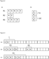
- Figure 2(a) shows three example combined resources R1, R2, and R3.
- R1 comprises five resource descriptors
- R2 comprises two resource descriptors
- R3 comprises four resource descriptors.
- the descriptors each identify the resource they belong to with a subscript.
- Letters A, B, C, and D denote the type of descriptor (e.g. texture, sampler, etc.).
- Figure 2(b) shows each of the types of descriptor from which combined resources R1, R2, and R3 can be described.
- Type A and B are shown as being retrieved by one unit, here for example, descriptors of type A and B are retrieved by the texture unit (TU).
- Type C and D are shown as being retrieved by a different unit to that of type A and B.
- descriptors of type C and D belong to the same category and are retrieved by a load store cache (LSC). It is desirable to store descriptors for resources used by the same unit of the GPU in similar locations of the cache memory. This makes retrieval of the descriptors needed by a particular unit more straightforward for that unit.
- LSC load store cache
- the unit may then assume that once it reaches a descriptor for a resource which is to be handled by another unit, it does not need to keep reading the descriptors of that particular combined resource anymore to be sure it has all the descriptors it will need.
- FIG. 3 illustrates three different cache lines implementing three different packing schemes. For simplicity in these examples all of the individual resource descriptors are the same size, and the cache lines comprise a small number of cells. Each cache has four cache lines of size L. Each cache line L has four equal cells of a minimum size.
- Figure 3(a) shows a cache with a first line comprising an A descriptor from combined resource R1, and a D descriptor from combined resource R2. This is an undesirable packing scheme. The descriptors of different combined resources are mixed together within the same cache line and the line would have to be accessed by both the TU and the LSC to obtain their respective descriptors. Figure 3(a) illustrates an undesirable packing scheme or no packing scheme.
- Figure 3(b) shows a cache comprising four cache lines.
- the combined resource R1 is larger than a single cache line, so the maximum combined resource size requires use of a multiple number of the cache lines in order to be stored.
- the maximum combined resource R1 is therefore formed into two groups and stored in the first two cache lines.
- An amount of padding may then be used to fill the rest of the second cache line so that only descriptors of R1 are stored in the second cache line. This may be achieved by forming the second group as a group of four descriptors comprising D1 and three units of padding.
- Combined resource R2 can then be stored in the next empty cache line, as shown in the third cache line of figure 3(b) .
- the remaining cache line can be used to store another combined resource descriptor.
- R3 may be stored in the fourth cache line, which is the next empty cache line after R2 (not shown).
- the only constraint that applies here is that the start address of the next combined resource descriptor needs to follow the alignment requirement for that combined resource descriptor. If the alignment condition can be satisfied alongside the multiple cache line size requirement of R1, then the next combined resource descriptor can be fitted in to a remaining cache line.
- An example implementation of this packing scheme may be, for each resource in combined resources: where 'sharpsize' denotes the size of a combined resource descriptor set, 'padding' is the space left between the end of the resource descriptor set and the start of a next cache line or next resource descriptor set, and 'addr' is the address of the cache line used.
- the proposed packing scheme it may be desired to reorder the descriptors of a combined resource to make the descriptors of the same category close together (i.e. the resources retrieved by the same GPU hardware unit). In this way the descriptors of the same category can be stored inside the same cache line(s).
- Figure 3(c) shows a cache where the maximum combined resource R1 is stored.
- the combined resource R1 is larger than a single cache line as in fig. 3 (a) .
- the resource descriptors of R1 have been separated by category and distributed accordingly over the two groups for the two cache lines used for storing R1.
- a simplified version of this embodiment is used for the purposes of explaining the concept.
- the series of groups formed as a result of this reordering are formed such that all of the resource descriptors within each group are of the same category.
- resource descriptors of a particular type may not initially be arranged adjacent to all the descriptors of the same type. In such a case the resource descriptors may need rearranging before they can be divided and stored in separate cache lines depending on their type.
- descriptors for any one resource are addressed by reference to the cache line in which they are stored. Therefore, it is noted that descriptors in different resources are not rearranged to be mixed together even if they contain resource descriptors of the same type and are stored in adjacent cache lines.
- the descriptors of similar types only need to be separated from the descriptors of the same resource of a different type by an amount equal to the remainder of the cache line used for the previous of the two descriptor types. That is, type ⁇ descriptors of resource A may take up 2.5 cache lines. Thus, a space of the remainder of the third cache line can be left blank to separate the type ⁇ descriptors from any type ⁇ descriptors in the rest of the descriptors of resource A.
- the modules of the GPU By separating the descriptors for a resource into different cache lines according to type it is possible to facilitate more efficient reading of the resource descriptors by the modules of the GPU. This is because different modules are responsible for using different resource descriptor types within the combined resource. If the descriptors of the same type are separated into different cache lines, the modules which require a specific type of resource descriptors can ignore cache lines which do not store any descriptors of that type. That is, in keeping with the above analogy, if module C only requires type ⁇ descriptors then it can ignore the cache lines which store the type ⁇ descriptors and skip straight to the cache lines which store the type ⁇ descriptors of the resource A. In this embodiment, the index entry of the resource A may indicate which cache line(s) have which type of descriptors in them.
- Figure 4(a) and (b) show an example of how descriptors may be shuffled or rearranged within the cache.
- Figure 4(a) shows a legend 402 with four different descriptor types. Different descriptor types may be fetched by the same GPU module, or by a different GPU module, depending on the type of descriptor and the purpose of the module in question. For example, in fig. 4(a) the top two descriptor types 404, 406, belong to one category which is fetched by the TU module. The bottom two descriptor types 408, 410, belong to another category which is fetched by the LSC module. Each module has the cache to store the descriptors. In the legend the sizes of the four different descriptors are indicated above the respective descriptors. The legend 402 identifies the different descriptors by type 404, 406, 408, 410 and category TU, LSC such that they can be easily identified in the cache memory 420 illustrated in figure 4(b) .
- Figure 4(b) shows a cache memory 420 which is linewise accessible and comprises eight 1 kilobit cache lines L.
- the top left cache line 412 contains both types of descriptors 408, 410 fetched by the LSC module.
- This cache line 412 can be fetched by the LSC module in its entirety. That is, without the need to avoid or unnecessarily fetch any descriptors which do not belong to a category handled by the LSC module.
- Descriptors located inside a single cache line which are of different types but belong to the same category can also be separated from each other by arranging them either side of any unused bits in that cache line. In this way the unused bits in the cache line, or the padding, can be used for a further purpose other than just causing the next category of descriptors of that resource or the descriptors of another resource to be stored in the next cache line.
- a combined Image and Sampler resource type could be made up of texture and sample type hardware descriptors. All Image/Texture/Sampler related resources would be fetched by the TU unit while Buffer/Storage related etc. would be fetched by the LSC unit. In the case where a Buffer is treated as an Image or an Image is treated as a Buffer an explicit API call may be done by the application.
- Figure 4(b) also shows how the descriptors of a specific category may be arranged within the cache memory such that they are located within similarly located lines of the cache memory. That is, the lines of the cache memory containing descriptors of the same category may be located within the cache memory in adjacent or near adjacent locations. This may be dependent on the size of the combined resource, the number of cache lines over which it is stored, and the same properties of the previous and next resource descriptor set. For example, the three cache lines in the top right corner of the cache memory as illustrated in fig. 4(b) all contain descriptors fetched by the TU module and are outlined by a thick boarder 414. These cache lines have been located one above the otherto optimise the fetching of these cache lines by the TU module. These cache lines may store descriptors for different resources. However, by being located adjacent to each other the TU module will be able to more efficiently fetch these cache lines should the different resources contained therein be fetched at similar times.
- An example implementation of the proposed packing scheme including a reordering of the descriptors based on category prior to storing in respective cache lines may be:
- 'set' is a set of resources
- 'sharp' is the hardware descriptor for each resource
- 'bindingid' is the resources that are used (excluding all other resources that are marked unused by the shader). Other resources could still be present but could be marked unused for a given instance of shader execution
- 'setid' is the loop index for each set
- 'cachelinesize' is the size of the cache line in bytes
- 'sharpsize' is the size of the hardware resource descriptor or data structure in bytes.
- Figure 5 shows a flow chart comprising the steps of the method 500 of arranging data and a set of data resource descriptors in a cache memory.
- the method determines a combined resource descriptor size and a cache line size such that one of those sizes is an integer multiple of the other one of those sizes. That is, the combined resource descriptor size may be of a magnitude such that it fits into a plurality of cache lines, all of which are needed to store the single combined resource descriptor.
- the cache line size may otherwise be a multiple of the combined resource descriptor size and multiple sets of data resource descriptors may fit into one cache line. This determination step enables the correct indexing of the addresses in the cache memory of the various resource descriptor sets.
- the data resource descriptor is the actual data which will be stored in the cache memory according to the proposed packing scheme.
- a plurality of non-overlapping storage areas are defined in the cache memory, each storage area being aligned to either (i) a line of the cache or (ii) a location offset from a line of the cache by an integer multiple of the determined combined resource descriptor size. That is, the plurality of non-overlapping storage areas may be arranged in the cache memory by aligning any one storage area to the start of a line of the cache, or by aligning any one storage area to a position within a line of the cache which is a certain distance away from the start of the line. The position away from the start of the line may be define by the amount of memory space between the start of the line and said position. The position may be chosen in dependence on the size in terms of memory of the largest combined resource descriptor. That is, the set of descriptors for a resource which is the biggest in term of memory space it takes up in the cache.
- step 508 a series of groups of data resource descriptors are formed, each group being of a size less than or equal to the combined resource descriptor size. That is, the combined resource descriptor may be divided into groups for storing in separate cache lines as for R1 in figures 3(b) and 3 (c) , or the combined resource descriptor may be a whole group which fits into a cache line as for R2 in figure 3(b) .
- each group of data resource descriptors may be stored in a respective one of the defined storage areas. That is, the groups as defined above may each be located in a different, separate part of the cache memory identified depending on the structure of the defined storage areas. As a result, the location of each of the groups can be identified individually without the need to identify other groups of descriptors in the same set.
- an additional step 512 may be carried out prior to the grouping step 508.
- step 512 the descriptors in the combined resource descriptor set are rearranged or shuffled such that descriptors of the same category (i.e. descriptors which are fetched by the same GPU hardware modules), are located in the same group as each other. Or rather, the defined groups contain descriptors which all belong to the same category. In this way the GPU modules which fetch a specific category of descriptors can efficiently find the descriptors they need from the cache memory, and do not need to fetch descriptors of different categories which they can't use and must then ignore.
- descriptors of the same category i.e. descriptors which are fetched by the same GPU hardware modules
- the above proposed packing scheme has advantages in that it allows the GPU to index the massive heterogeneous descriptor array which results from combining the resource descriptors. It also reduces the driver overhead by using a straightforward and simple to implement alignment rule. Additionally, the proposed resource packing scheme is good for the GPU hardware as it may support an internal dedicated cache for caching and keeping the hardware descriptors for future use.
- the hardware TU fetch the cache line 1 Kbit, which contains T# and S# only.
- the hardware LSC fetch the cache line 1 Kbit, which contains U# and C# only.
- FIG. 6 is a high level data flow block diagram which shows the relevant GPU hardware component blocks and their interactions with software at the CPU via 'Job Descriptors' data structures of the shared memory. Arrows illustrate the direction of the data flow between the various software and hardware system components as described herein.
- index_offset is computed. This requires the value offset(setld, bindingld)/stride to be calculated, and is followed by filling the index_offset in the internal uniform of the descriptor.
- the compile time size is also known to the compiler (e.g. how the structures are packed or not fully packed). The same principle applies here. This depends on the definition of these resource types as written inside the shader code (not in the driver runtime code implementing these APIs).
- the index offset size has to be calculated by the shader compiler during runtime on the CPU (host) before execution of the shader, then passed on to the driver using the compiler driver interface. This information is then set inside hardware descriptors by the driver, coming from the compiler, to be used by the hardware for shader execution.
- the compiler instructions for indexing the set of resource descriptors relating to a function are added to such that an offset value is added.
- the offset value corresponds to an offset location in a respective storage area of the set of resource descriptors.
- the instructions are stored in the same storage area as the resource descriptors for that function. That is, to support the dynamic indexing feature for combined resources, the compiler needs to insert an instruction to add the index with the offset location of the combined resource into the shader code to calculate the final index.
- GPR general purpose register
- crd[3] there may be an array combined resource descriptor, crd[3], and when executing the shader code it tries to index the ith combined resource by using syntax crd[i], where i is a value in the set [0, 2].
- the compiler will insert an add instruction to calculate the final index as i + offset index, the offset index being based on the size calculated at the driver.
- Descriptors may also be referred to as sharps, which are the meta data stored in the memory for the shader resource.
- a T sharp may include the address, texture dimension and so on for the texture.
- An S sharp may include the address, filtering mode and so on for the sampler.
- the descriptor or sharp size can be different.
- Vulkan defines different descriptor types for the shader resource. Each descriptor type maps to one sharp. Combined resource in this context means that mixed sharps can be in one array, which supports dynamic uniform and non-uniform indexing.
Landscapes
- Engineering & Computer Science (AREA)
- Theoretical Computer Science (AREA)
- Physics & Mathematics (AREA)
- General Physics & Mathematics (AREA)
- General Engineering & Computer Science (AREA)
- Memory System Of A Hierarchy Structure (AREA)
- Image Generation (AREA)
Claims (15)
- Datenprozessor, konfiguriert zum Anordnen von Daten und einer Menge von Datenbetriebsmittel-Deskriptoren (106) in einem Zwischenspeicher (420),
wobei die Menge von Datenbetriebsmittel-Deskriptoren Datenbetriebsmittel-Deskriptoren verschiedener Typen und verschiedener Größen umfasst, wobei der Zwischenspeicher zeilenweise durch ein Datenverarbeitungsgerät zugänglich ist, wobei der Datenprozessor konfiguriert ist zum:Bestimmen einer kombinierten Betriebsmitteldeskriptor-Größe und einer Zwischenspeicherzeile-Größe (102) derart, dass eine dieser Größen ein ganzzahliges Vielfaches der anderen einen dieser Größen ist;Empfangen der Datenbetriebsmittel-Deskriptoren;Definieren einer Vielzahl von nicht überlappenden Speicherbereichen in dem Zwischenspeicher, wobei jeder Speicherbereich mit entweder (i) einer Zeile des Zwischenspeichers oder (ii) einem Ort, der von einer Zeile des Zwischenspeichers um ein ganzzahliges Vielfaches der bestimmten kombinierten Betriebsmitteldeskriptor-Größe versetzt ist, ausgerichtet ist;Bilden einer Reihe von Gruppen von Datenbetriebsmittel-Deskriptoren, wobei jede Gruppe eine Größe aufweist, die kleiner als die oder gleich der kombinierten Betriebsmitteldeskriptor-Größe ist; undSpeichern jeder Gruppe von Datenbetriebsmittel-Deskriptoren in einem jeweiligen einen der Vielzahl der definierten nicht überlappenden Speicherbereiche. - Datenprozessor nach Anspruch 1, wobei jeder Datenbetriebsmittel-Deskriptor eine Kategorie aufweist, basierend auf der eine Vielzahl von Hardware-Einheiten verwendet wird, den Datenbetriebsmittel-Deskriptor aus dem Zwischenspeicher zu holen, und der Datenprozessor konfiguriert ist zum, vor dem Schritt des Bildens einer Reihe von Gruppen, Umordnen der kombinierten Betriebsmitteldeskriptoren derart, dass alle Datenbetriebsmittel-Deskriptoren in jeder Gruppe die gleiche Kategorie aufweisen.
- Datenprozessor nach einem der vorhergehenden Ansprüche, wobei die kombinierte Betriebsmitteldeskriptor-Größe die maximale kombinierte Größe der Datenbetriebsmittel-Deskriptoren ist, die erforderlich ist, eine einzelne Aktion zu beschreiben.
- Datenprozessor nach einem der vorhergehenden Ansprüche, wobei die kombinierte Betriebsmitteldeskriptor-Größe ein ganzzahliges Vielfaches der Zwischenspeicherzeilen-Größe ist.
- Datenprozessor nach einem der vorhergehenden Ansprüche, wobei die Zwischenspeicherzeilen-Größe ein ganzzahliges Vielfaches der kombinierten Betriebsmitteldeskriptor-Größe ist.
- Datenprozessor nach einem der vorhergehenden Ansprüche, wobei die Datenbetriebsmittel-Deskriptoren eine beliebige Kombination von heterogenen Betriebsmitteltypen, die ein beliebiges einer Textur, eines Abtasters, eines Puffers oder eines Bilds umfassen, beschreiben.
- Datenprozessor nach einem der vorhergehenden Ansprüche, wobei der Datenprozessor eine Grafikprozessoreinheit ist.
- Verfahren (500) zum Anordnen von Daten und einer Menge von Datenbetriebsmittel-Deskriptoren in einem Zwischenspeicher, wobei die Menge von Datenbetriebsmittel-Deskriptoren Datenbetriebsmittel-Deskriptoren verschiedener Typen und verschiedener Größen umfasst, wobei der Zwischenspeicher zeilenweise durch ein Datenverarbeitungsgerät zugänglich ist, das Verfahren umfassend:Bestimmen (602) einer kombinierten Betriebsmitteldeskriptor-Größe und einer Zwischenspeicherzeilen-Größe derart, dass eine dieser Größen ein ganzzahliges Vielfaches der anderen dieser Größen ist;Empfangen (504) der Datenbetriebsmittel-Deskriptoren;Definieren (506) einer Vielzahl von nicht überlappenden Speicherbereichen in dem Zwischenspeicher, wobei jeder Speicherbereich mit entweder (i) einer Zeile des Zwischenspeichers oder (ii) einem Ort, der von einer Zeile des Zwischenspeichers um ein ganzzahliges Vielfaches der bestimmten kombinierten Betriebsmitteldeskriptor-Größe versetzt ist, ausgerichtet ist;Bilden (508) einer Reihe von Gruppen von Datenbetriebsmittel-Deskriptoren, wobei jede Gruppe eine Größe aufweist, die kleiner als die oder gleich der kombinierten Betriebsmitteldeskriptor-Größe ist; undSpeichern (510) jeder Gruppe von Datenbetriebsmittel-Deskriptoren in einem jeweiligen einen der Vielzahl der definierten nicht überlappenden Speicherbereiche.
- Verfahren (500) nach Anspruch 8, wobei das Verfahren (500) umfasst, vor dem Schritt des Bildens (508) einer Reihe von Gruppen die Datenbetriebsmittel-Deskriptoren derart umzuordnen (512), dass die Datenbetriebsmittel-Deskriptoren in jeder Gruppe die gleiche Kategorie aufweisen.
- Verfahren (500) nach Anspruch 8 oder 9, wobei die kombinierte Betriebsmitteldeskriptor-Größe ein ganzzahliges Vielfaches der Zwischenspeicherzeilen-Größe ist.
- Verfahren (500) nach einem der Ansprüche 8 bis 10, wobei die Zwischenspeicherzeilen-Größe ein ganzzahliges Vielfaches der kombinierten Betriebsmitteldeskriptor-Größe ist.
- Verfahren (500) nach einem der Ansprüche 8 bis 11, wobei ein Datenfluss des Verfahrens von einem Treiber zu einem Compiler zu einer Grafikprozessoreinheit ist.
- Verfahren (500) nach Anspruch 12, wobei der Treiber konfiguriert ist zum Berechnen der Größe jeder der Speicherbereiche und für jede einer Menge von Funktionen, wobei jede Funktion mit einem Satz einer oder mehrerer der Gruppen von Datenbetriebsmittel-Deskriptoren assoziiert ist, Speichern der Datenbetriebsmittel-Deskriptoren jeder Gruppe dieser Menge in einem einzelnen Speicherbereich.
- Verfahren (500) nach Anspruch 13, wobei der Compiler konfiguriert ist zum Hinzufügen der Anweisungen zum Indexieren der Menge von Datenbetriebsmittel-Deskriptoren bezüglich einer Funktion derart, dass ein Versatzwert, der mit einem Versatzort in einem jeweiligen Speicherbereich der Menge von Datenbetriebsmittel-Deskriptoren korrespondiert, hinzugefügt wird, und zum Speichern dieser Anweisungen in demselben Speicherbereich wie die Datenbetriebsmittel-Deskriptoren für diese Funktion.
- Gerät, umfassend den Datenprozessor nach einem der Ansprüche 1 bis 7, der das Verfahren nach einem der Ansprüche 8 bis 11 ausführt, und eine CPU, die das Verfahren nach einem der Ansprüche 12 bis 14 ausführt.
Applications Claiming Priority (1)
| Application Number | Priority Date | Filing Date | Title |
|---|---|---|---|
| PCT/CN2020/092265 WO2021237441A1 (en) | 2020-05-26 | 2020-05-26 | Device and method for data packing in memory |
Publications (3)
| Publication Number | Publication Date |
|---|---|
| EP4111306A1 EP4111306A1 (de) | 2023-01-04 |
| EP4111306A4 EP4111306A4 (de) | 2023-05-03 |
| EP4111306B1 true EP4111306B1 (de) | 2024-11-27 |
Family
ID=78745137
Family Applications (1)
| Application Number | Title | Priority Date | Filing Date |
|---|---|---|---|
| EP20938146.6A Active EP4111306B1 (de) | 2020-05-26 | 2020-05-26 | Vorrichtung und verfahren zur datenpackung in einem speicher |
Country Status (2)
| Country | Link |
|---|---|
| EP (1) | EP4111306B1 (de) |
| WO (1) | WO2021237441A1 (de) |
Family Cites Families (7)
| Publication number | Priority date | Publication date | Assignee | Title |
|---|---|---|---|---|
| US7403952B2 (en) | 2000-12-28 | 2008-07-22 | International Business Machines Corporation | Numa system resource descriptors including performance characteristics |
| US7999819B2 (en) | 2007-11-20 | 2011-08-16 | Via Technologies, Inc. | Systems and methods for managing texture descriptors in a shared texture engine |
| US10032246B2 (en) * | 2013-10-09 | 2018-07-24 | Nvidia Corporation | Approach to caching decoded texture data with variable dimensions |
| WO2015130837A1 (en) | 2014-02-25 | 2015-09-03 | Dynavisor, Inc. | Dynamic information virtualization |
| US9947071B2 (en) * | 2014-06-27 | 2018-04-17 | Samsung Electronics Co., Ltd. | Texture pipeline with online variable rate dictionary compression |
| US9892053B2 (en) * | 2015-03-24 | 2018-02-13 | Intel Corporation | Compaction for memory hierarchies |
| US10055810B2 (en) * | 2016-03-04 | 2018-08-21 | Samsung Electronics Co., Ltd. | Cache architecture for efficiently accessing texture data using buffers |
-
2020
- 2020-05-26 EP EP20938146.6A patent/EP4111306B1/de active Active
- 2020-05-26 WO PCT/CN2020/092265 patent/WO2021237441A1/en not_active Ceased
Also Published As
| Publication number | Publication date |
|---|---|
| WO2021237441A1 (en) | 2021-12-02 |
| EP4111306A4 (de) | 2023-05-03 |
| EP4111306A1 (de) | 2023-01-04 |
Similar Documents
| Publication | Publication Date | Title |
|---|---|---|
| EP3274841B1 (de) | Verdichtung von speicherhierarchien | |
| US6862027B2 (en) | System and method for parallel execution of data generation tasks | |
| EP2834792B1 (de) | Patch-basiertes shading in der grafikverarbeitung | |
| US10282808B2 (en) | Hierarchical lossless compression and null data support | |
| EP2939208B1 (de) | System zum rendern von spritegrafiken | |
| US7355601B2 (en) | System and method for transfer of data between processors using a locked set, head and tail pointers | |
| US7705846B1 (en) | Processing high numbers of independent textures in a 3-D graphics pipeline | |
| US20020085010A1 (en) | Method and apparatus for tiled polygon traversal | |
| US9922396B2 (en) | Reduction of BVH-node bandwidth with incremental traversal | |
| KR20010085424A (ko) | 지연 쉐이딩을 갖는 그래픽 프로세서 | |
| US20170372448A1 (en) | Reducing Memory Access Latencies During Ray Traversal | |
| US7170512B2 (en) | Index processor | |
| US10466915B2 (en) | Accessing encoded blocks of data in memory | |
| US20220301228A1 (en) | Variable width interleaved coding for graphics processing | |
| WO2015183855A1 (en) | Graphics pipeline state object and model | |
| CN113838180B (zh) | 一种渲染指令处理方法及其相关设备 | |
| JP2023525725A (ja) | データ圧縮の方法及び装置 | |
| US6862028B2 (en) | Bin pointer and state caching apparatus and method | |
| EP4111306B1 (de) | Vorrichtung und verfahren zur datenpackung in einem speicher | |
| CN109643279B (zh) | 使用虚拟到虚拟地址表进行存储器压缩的方法和装置 | |
| US11150943B2 (en) | Enabling a single context hardware system to operate as a multi-context system | |
| US7945757B1 (en) | Conserving and shaping address space with arrays | |
| US20180032431A1 (en) | Banking Graphics Processor Shared Local Memory | |
| US8095746B1 (en) | Conserving and shaping address space with arrays | |
| US20240169474A1 (en) | Graphics processing |
Legal Events
| Date | Code | Title | Description |
|---|---|---|---|
| STAA | Information on the status of an ep patent application or granted ep patent |
Free format text: STATUS: THE INTERNATIONAL PUBLICATION HAS BEEN MADE |
|
| PUAI | Public reference made under article 153(3) epc to a published international application that has entered the european phase |
Free format text: ORIGINAL CODE: 0009012 |
|
| STAA | Information on the status of an ep patent application or granted ep patent |
Free format text: STATUS: REQUEST FOR EXAMINATION WAS MADE |
|
| 17P | Request for examination filed |
Effective date: 20220926 |
|
| AK | Designated contracting states |
Kind code of ref document: A1 Designated state(s): AL AT BE BG CH CY CZ DE DK EE ES FI FR GB GR HR HU IE IS IT LI LT LU LV MC MK MT NL NO PL PT RO RS SE SI SK SM TR |
|
| REG | Reference to a national code |
Ref country code: DE Ref legal event code: R079 Free format text: PREVIOUS MAIN CLASS: G06F0009455000 Ipc: G06F0012088600 Ref document number: 602020042314 Country of ref document: DE |
|
| A4 | Supplementary search report drawn up and despatched |
Effective date: 20230330 |
|
| RIC1 | Information provided on ipc code assigned before grant |
Ipc: G06F 12/0895 20160101ALN20230324BHEP Ipc: G06F 9/455 20180101ALI20230324BHEP Ipc: G06F 12/0875 20160101ALI20230324BHEP Ipc: G06T 1/60 20060101ALI20230324BHEP Ipc: G06F 12/0879 20160101ALI20230324BHEP Ipc: G06F 12/0886 20160101AFI20230324BHEP |
|
| DAV | Request for validation of the european patent (deleted) | ||
| DAX | Request for extension of the european patent (deleted) | ||
| GRAP | Despatch of communication of intention to grant a patent |
Free format text: ORIGINAL CODE: EPIDOSNIGR1 |
|
| STAA | Information on the status of an ep patent application or granted ep patent |
Free format text: STATUS: GRANT OF PATENT IS INTENDED |
|
| RIC1 | Information provided on ipc code assigned before grant |
Ipc: G06F 12/0895 20160101ALN20240612BHEP Ipc: G06F 9/455 20180101ALI20240612BHEP Ipc: G06F 12/0875 20160101ALI20240612BHEP Ipc: G06T 1/60 20060101ALI20240612BHEP Ipc: G06F 12/0879 20160101ALI20240612BHEP Ipc: G06F 12/0886 20160101AFI20240612BHEP |
|
| INTG | Intention to grant announced |
Effective date: 20240705 |
|
| RIN1 | Information on inventor provided before grant (corrected) |
Inventor name: ZHU, YUNPENG Inventor name: PRASAD, VATSALYA |
|
| GRAS | Grant fee paid |
Free format text: ORIGINAL CODE: EPIDOSNIGR3 |
|
| GRAA | (expected) grant |
Free format text: ORIGINAL CODE: 0009210 |
|
| STAA | Information on the status of an ep patent application or granted ep patent |
Free format text: STATUS: THE PATENT HAS BEEN GRANTED |
|
| AK | Designated contracting states |
Kind code of ref document: B1 Designated state(s): AL AT BE BG CH CY CZ DE DK EE ES FI FR GB GR HR HU IE IS IT LI LT LU LV MC MK MT NL NO PL PT RO RS SE SI SK SM TR |
|
| REG | Reference to a national code |
Ref country code: GB Ref legal event code: FG4D |
|
| REG | Reference to a national code |
Ref country code: CH Ref legal event code: EP |
|
| REG | Reference to a national code |
Ref country code: DE Ref legal event code: R096 Ref document number: 602020042314 Country of ref document: DE |
|
| REG | Reference to a national code |
Ref country code: IE Ref legal event code: FG4D |
|
| REG | Reference to a national code |
Ref country code: LT Ref legal event code: MG9D |
|
| REG | Reference to a national code |
Ref country code: NL Ref legal event code: MP Effective date: 20241127 |
|
| PG25 | Lapsed in a contracting state [announced via postgrant information from national office to epo] |
Ref country code: HR Free format text: LAPSE BECAUSE OF FAILURE TO SUBMIT A TRANSLATION OF THE DESCRIPTION OR TO PAY THE FEE WITHIN THE PRESCRIBED TIME-LIMIT Effective date: 20241127 Ref country code: PT Free format text: LAPSE BECAUSE OF FAILURE TO SUBMIT A TRANSLATION OF THE DESCRIPTION OR TO PAY THE FEE WITHIN THE PRESCRIBED TIME-LIMIT Effective date: 20250327 Ref country code: IS Free format text: LAPSE BECAUSE OF FAILURE TO SUBMIT A TRANSLATION OF THE DESCRIPTION OR TO PAY THE FEE WITHIN THE PRESCRIBED TIME-LIMIT Effective date: 20250327 |
|
| PG25 | Lapsed in a contracting state [announced via postgrant information from national office to epo] |
Ref country code: FI Free format text: LAPSE BECAUSE OF FAILURE TO SUBMIT A TRANSLATION OF THE DESCRIPTION OR TO PAY THE FEE WITHIN THE PRESCRIBED TIME-LIMIT Effective date: 20241127 Ref country code: NL Free format text: LAPSE BECAUSE OF FAILURE TO SUBMIT A TRANSLATION OF THE DESCRIPTION OR TO PAY THE FEE WITHIN THE PRESCRIBED TIME-LIMIT Effective date: 20241127 |
|
| REG | Reference to a national code |
Ref country code: AT Ref legal event code: MK05 Ref document number: 1746356 Country of ref document: AT Kind code of ref document: T Effective date: 20241127 |
|
| PG25 | Lapsed in a contracting state [announced via postgrant information from national office to epo] |
Ref country code: BG Free format text: LAPSE BECAUSE OF FAILURE TO SUBMIT A TRANSLATION OF THE DESCRIPTION OR TO PAY THE FEE WITHIN THE PRESCRIBED TIME-LIMIT Effective date: 20241127 |
|
| PG25 | Lapsed in a contracting state [announced via postgrant information from national office to epo] |
Ref country code: ES Free format text: LAPSE BECAUSE OF FAILURE TO SUBMIT A TRANSLATION OF THE DESCRIPTION OR TO PAY THE FEE WITHIN THE PRESCRIBED TIME-LIMIT Effective date: 20241127 |
|
| PG25 | Lapsed in a contracting state [announced via postgrant information from national office to epo] |
Ref country code: NO Free format text: LAPSE BECAUSE OF FAILURE TO SUBMIT A TRANSLATION OF THE DESCRIPTION OR TO PAY THE FEE WITHIN THE PRESCRIBED TIME-LIMIT Effective date: 20250227 |
|
| PG25 | Lapsed in a contracting state [announced via postgrant information from national office to epo] |
Ref country code: LV Free format text: LAPSE BECAUSE OF FAILURE TO SUBMIT A TRANSLATION OF THE DESCRIPTION OR TO PAY THE FEE WITHIN THE PRESCRIBED TIME-LIMIT Effective date: 20241127 Ref country code: GR Free format text: LAPSE BECAUSE OF FAILURE TO SUBMIT A TRANSLATION OF THE DESCRIPTION OR TO PAY THE FEE WITHIN THE PRESCRIBED TIME-LIMIT Effective date: 20250228 Ref country code: AT Free format text: LAPSE BECAUSE OF FAILURE TO SUBMIT A TRANSLATION OF THE DESCRIPTION OR TO PAY THE FEE WITHIN THE PRESCRIBED TIME-LIMIT Effective date: 20241127 |
|
| PG25 | Lapsed in a contracting state [announced via postgrant information from national office to epo] |
Ref country code: PL Free format text: LAPSE BECAUSE OF FAILURE TO SUBMIT A TRANSLATION OF THE DESCRIPTION OR TO PAY THE FEE WITHIN THE PRESCRIBED TIME-LIMIT Effective date: 20241127 |
|
| PG25 | Lapsed in a contracting state [announced via postgrant information from national office to epo] |
Ref country code: RS Free format text: LAPSE BECAUSE OF FAILURE TO SUBMIT A TRANSLATION OF THE DESCRIPTION OR TO PAY THE FEE WITHIN THE PRESCRIBED TIME-LIMIT Effective date: 20250227 |
|
| PG25 | Lapsed in a contracting state [announced via postgrant information from national office to epo] |
Ref country code: SM Free format text: LAPSE BECAUSE OF FAILURE TO SUBMIT A TRANSLATION OF THE DESCRIPTION OR TO PAY THE FEE WITHIN THE PRESCRIBED TIME-LIMIT Effective date: 20241127 |
|
| PGFP | Annual fee paid to national office [announced via postgrant information from national office to epo] |
Ref country code: DE Payment date: 20250402 Year of fee payment: 6 |
|
| PG25 | Lapsed in a contracting state [announced via postgrant information from national office to epo] |
Ref country code: DK Free format text: LAPSE BECAUSE OF FAILURE TO SUBMIT A TRANSLATION OF THE DESCRIPTION OR TO PAY THE FEE WITHIN THE PRESCRIBED TIME-LIMIT Effective date: 20241127 |
|
| PG25 | Lapsed in a contracting state [announced via postgrant information from national office to epo] |
Ref country code: EE Free format text: LAPSE BECAUSE OF FAILURE TO SUBMIT A TRANSLATION OF THE DESCRIPTION OR TO PAY THE FEE WITHIN THE PRESCRIBED TIME-LIMIT Effective date: 20241127 |
|
| PG25 | Lapsed in a contracting state [announced via postgrant information from national office to epo] |
Ref country code: RO Free format text: LAPSE BECAUSE OF FAILURE TO SUBMIT A TRANSLATION OF THE DESCRIPTION OR TO PAY THE FEE WITHIN THE PRESCRIBED TIME-LIMIT Effective date: 20241127 |
|
| PG25 | Lapsed in a contracting state [announced via postgrant information from national office to epo] |
Ref country code: SK Free format text: LAPSE BECAUSE OF FAILURE TO SUBMIT A TRANSLATION OF THE DESCRIPTION OR TO PAY THE FEE WITHIN THE PRESCRIBED TIME-LIMIT Effective date: 20241127 |
|
| PG25 | Lapsed in a contracting state [announced via postgrant information from national office to epo] |
Ref country code: CZ Free format text: LAPSE BECAUSE OF FAILURE TO SUBMIT A TRANSLATION OF THE DESCRIPTION OR TO PAY THE FEE WITHIN THE PRESCRIBED TIME-LIMIT Effective date: 20241127 |
|
| PG25 | Lapsed in a contracting state [announced via postgrant information from national office to epo] |
Ref country code: IT Free format text: LAPSE BECAUSE OF FAILURE TO SUBMIT A TRANSLATION OF THE DESCRIPTION OR TO PAY THE FEE WITHIN THE PRESCRIBED TIME-LIMIT Effective date: 20241127 |
|
| REG | Reference to a national code |
Ref country code: DE Ref legal event code: R097 Ref document number: 602020042314 Country of ref document: DE |
|
| PG25 | Lapsed in a contracting state [announced via postgrant information from national office to epo] |
Ref country code: SE Free format text: LAPSE BECAUSE OF FAILURE TO SUBMIT A TRANSLATION OF THE DESCRIPTION OR TO PAY THE FEE WITHIN THE PRESCRIBED TIME-LIMIT Effective date: 20241127 |
|
| PLBE | No opposition filed within time limit |
Free format text: ORIGINAL CODE: 0009261 |
|
| STAA | Information on the status of an ep patent application or granted ep patent |
Free format text: STATUS: NO OPPOSITION FILED WITHIN TIME LIMIT |
|
| 26N | No opposition filed |
Effective date: 20250828 |