EP4109566A1 - Display device - Google Patents
Display device Download PDFInfo
- Publication number
- EP4109566A1 EP4109566A1 EP21778712.6A EP21778712A EP4109566A1 EP 4109566 A1 EP4109566 A1 EP 4109566A1 EP 21778712 A EP21778712 A EP 21778712A EP 4109566 A1 EP4109566 A1 EP 4109566A1
- Authority
- EP
- European Patent Office
- Prior art keywords
- light emitting
- emitting diode
- pixels
- emitting unit
- diode element
- Prior art date
- Legal status (The legal status is an assumption and is not a legal conclusion. Google has not performed a legal analysis and makes no representation as to the accuracy of the status listed.)
- Pending
Links
Images






Classifications
-
- H—ELECTRICITY
- H10—SEMICONDUCTOR DEVICES; ELECTRIC SOLID-STATE DEVICES NOT OTHERWISE PROVIDED FOR
- H10K—ORGANIC ELECTRIC SOLID-STATE DEVICES
- H10K59/00—Integrated devices, or assemblies of multiple devices, comprising at least one organic light-emitting element covered by group H10K50/00
- H10K59/30—Devices specially adapted for multicolour light emission
- H10K59/35—Devices specially adapted for multicolour light emission comprising red-green-blue [RGB] subpixels
- H10K59/351—Devices specially adapted for multicolour light emission comprising red-green-blue [RGB] subpixels comprising more than three subpixels, e.g. red-green-blue-white [RGBW]
-
- H—ELECTRICITY
- H10—SEMICONDUCTOR DEVICES; ELECTRIC SOLID-STATE DEVICES NOT OTHERWISE PROVIDED FOR
- H10W—GENERIC PACKAGES, INTERCONNECTIONS, CONNECTORS OR OTHER CONSTRUCTIONAL DETAILS OF DEVICES COVERED BY CLASS H10
- H10W90/00—Package configurations
-
- G—PHYSICS
- G09—EDUCATION; CRYPTOGRAPHY; DISPLAY; ADVERTISING; SEALS
- G09F—DISPLAYING; ADVERTISING; SIGNS; LABELS OR NAME-PLATES; SEALS
- G09F9/00—Indicating arrangements for variable information in which the information is built-up on a support by selection or combination of individual elements
- G09F9/30—Indicating arrangements for variable information in which the information is built-up on a support by selection or combination of individual elements in which the desired character or characters are formed by combining individual elements
- G09F9/302—Indicating arrangements for variable information in which the information is built-up on a support by selection or combination of individual elements in which the desired character or characters are formed by combining individual elements characterised by the form or geometrical disposition of the individual elements
-
- G—PHYSICS
- G09—EDUCATION; CRYPTOGRAPHY; DISPLAY; ADVERTISING; SEALS
- G09F—DISPLAYING; ADVERTISING; SIGNS; LABELS OR NAME-PLATES; SEALS
- G09F9/00—Indicating arrangements for variable information in which the information is built-up on a support by selection or combination of individual elements
- G09F9/30—Indicating arrangements for variable information in which the information is built-up on a support by selection or combination of individual elements in which the desired character or characters are formed by combining individual elements
- G09F9/33—Indicating arrangements for variable information in which the information is built-up on a support by selection or combination of individual elements in which the desired character or characters are formed by combining individual elements being semiconductor devices, e.g. diodes
-
- G—PHYSICS
- G09—EDUCATION; CRYPTOGRAPHY; DISPLAY; ADVERTISING; SEALS
- G09G—ARRANGEMENTS OR CIRCUITS FOR CONTROL OF INDICATING DEVICES USING STATIC MEANS TO PRESENT VARIABLE INFORMATION
- G09G3/00—Control arrangements or circuits, of interest only in connection with visual indicators other than cathode-ray tubes
- G09G3/20—Control arrangements or circuits, of interest only in connection with visual indicators other than cathode-ray tubes for presentation of an assembly of a number of characters, e.g. a page, by composing the assembly by combination of individual elements arranged in a matrix no fixed position being assigned to or needed to be assigned to the individual characters or partial characters
- G09G3/2003—Display of colours
-
- G—PHYSICS
- G09—EDUCATION; CRYPTOGRAPHY; DISPLAY; ADVERTISING; SEALS
- G09G—ARRANGEMENTS OR CIRCUITS FOR CONTROL OF INDICATING DEVICES USING STATIC MEANS TO PRESENT VARIABLE INFORMATION
- G09G3/00—Control arrangements or circuits, of interest only in connection with visual indicators other than cathode-ray tubes
- G09G3/20—Control arrangements or circuits, of interest only in connection with visual indicators other than cathode-ray tubes for presentation of an assembly of a number of characters, e.g. a page, by composing the assembly by combination of individual elements arranged in a matrix no fixed position being assigned to or needed to be assigned to the individual characters or partial characters
- G09G3/22—Control arrangements or circuits, of interest only in connection with visual indicators other than cathode-ray tubes for presentation of an assembly of a number of characters, e.g. a page, by composing the assembly by combination of individual elements arranged in a matrix no fixed position being assigned to or needed to be assigned to the individual characters or partial characters using controlled light sources
- G09G3/30—Control arrangements or circuits, of interest only in connection with visual indicators other than cathode-ray tubes for presentation of an assembly of a number of characters, e.g. a page, by composing the assembly by combination of individual elements arranged in a matrix no fixed position being assigned to or needed to be assigned to the individual characters or partial characters using controlled light sources using electroluminescent panels
- G09G3/32—Control arrangements or circuits, of interest only in connection with visual indicators other than cathode-ray tubes for presentation of an assembly of a number of characters, e.g. a page, by composing the assembly by combination of individual elements arranged in a matrix no fixed position being assigned to or needed to be assigned to the individual characters or partial characters using controlled light sources using electroluminescent panels semiconductive, e.g. using light-emitting diodes [LED]
-
- H—ELECTRICITY
- H10—SEMICONDUCTOR DEVICES; ELECTRIC SOLID-STATE DEVICES NOT OTHERWISE PROVIDED FOR
- H10H—INORGANIC LIGHT-EMITTING SEMICONDUCTOR DEVICES HAVING POTENTIAL BARRIERS
- H10H20/00—Individual inorganic light-emitting semiconductor devices having potential barriers, e.g. light-emitting diodes [LED]
- H10H20/80—Constructional details
- H10H20/85—Packages
- H10H20/851—Wavelength conversion means
- H10H20/8511—Wavelength conversion means characterised by their material, e.g. binder
- H10H20/8512—Wavelength conversion materials
-
- H—ELECTRICITY
- H10—SEMICONDUCTOR DEVICES; ELECTRIC SOLID-STATE DEVICES NOT OTHERWISE PROVIDED FOR
- H10H—INORGANIC LIGHT-EMITTING SEMICONDUCTOR DEVICES HAVING POTENTIAL BARRIERS
- H10H20/00—Individual inorganic light-emitting semiconductor devices having potential barriers, e.g. light-emitting diodes [LED]
- H10H20/80—Constructional details
- H10H20/85—Packages
- H10H20/852—Encapsulations
-
- H—ELECTRICITY
- H10—SEMICONDUCTOR DEVICES; ELECTRIC SOLID-STATE DEVICES NOT OTHERWISE PROVIDED FOR
- H10H—INORGANIC LIGHT-EMITTING SEMICONDUCTOR DEVICES HAVING POTENTIAL BARRIERS
- H10H29/00—Integrated devices, or assemblies of multiple devices, comprising at least one light-emitting semiconductor element covered by group H10H20/00
- H10H29/10—Integrated devices comprising at least one light-emitting semiconductor component covered by group H10H20/00
- H10H29/14—Integrated devices comprising at least one light-emitting semiconductor component covered by group H10H20/00 comprising multiple light-emitting semiconductor components
- H10H29/142—Two-dimensional arrangements, e.g. asymmetric LED layout
-
- H—ELECTRICITY
- H10—SEMICONDUCTOR DEVICES; ELECTRIC SOLID-STATE DEVICES NOT OTHERWISE PROVIDED FOR
- H10K—ORGANIC ELECTRIC SOLID-STATE DEVICES
- H10K59/00—Integrated devices, or assemblies of multiple devices, comprising at least one organic light-emitting element covered by group H10K50/00
- H10K59/30—Devices specially adapted for multicolour light emission
- H10K59/38—Devices specially adapted for multicolour light emission comprising colour filters or colour changing media [CCM]
-
- G—PHYSICS
- G09—EDUCATION; CRYPTOGRAPHY; DISPLAY; ADVERTISING; SEALS
- G09G—ARRANGEMENTS OR CIRCUITS FOR CONTROL OF INDICATING DEVICES USING STATIC MEANS TO PRESENT VARIABLE INFORMATION
- G09G2300/00—Aspects of the constitution of display devices
- G09G2300/04—Structural and physical details of display devices
- G09G2300/0439—Pixel structures
- G09G2300/0452—Details of colour pixel setup, e.g. pixel composed of a red, a blue and two green components
-
- H—ELECTRICITY
- H10—SEMICONDUCTOR DEVICES; ELECTRIC SOLID-STATE DEVICES NOT OTHERWISE PROVIDED FOR
- H10K—ORGANIC ELECTRIC SOLID-STATE DEVICES
- H10K2102/00—Constructional details relating to the organic devices covered by this subclass
- H10K2102/301—Details of OLEDs
Definitions
- the present disclosure relates to a display device.
- LED elements light emitting diode elements
- one pixel includes LEDs of three colors of red (R), green (G), and blue (B) (see Patent Document 1, for example).
- Patent Document 1 Japanese Patent Application Laid-Open No. 2001-75508
- An object of the present disclosure is to provide a display device capable of reducing the number of wirings on a substrate and simplifying manufacturing by changing the pixel configuration.
- a display device including:
- a display device including:
- a display device including:
- a display device including:
- the sense of resolution is not largely affected even if blue LED elements are thinned out from pixels having LED elements of three colors of red, green, and blue. Furthermore, since the resolution and recognition for the color red is less visible than the color green, the sense of resolution is not largely affected even if red LED elements are thinned out from pixels having LED elements of three colors.
- a plurality of first pixels having LED elements of two colors of red and green and a plurality of second pixels having LED elements of two colors of green and blue are two-dimensionally arranged on the basis of the above viewpoint.
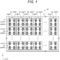
- Fig. 1 is a plan view of a display device 10 according to a first embodiment of the present disclosure.
- the display device 10 is a so-called LED display device, and includes a substrate 11 and a plurality of surface mount devices (hereinafter referred to as "SMDs") 12 provided on the substrate 11.
- SMDs surface mount devices
- the substrate 11 is, for example, a printed circuit board (PCB).
- PCB printed circuit board
- a plurality of scanning lines, a plurality of signal lines, and driver integrated circuits (IC) for controlling the plurality of SMDs 12 via the plurality of scanning lines and the plurality of signal lines are provided on the substrate 11.
- the plurality of SMDs 12 is two-dimensionally arranged in a lattice shape on the substrate 11.
- a row direction of the twodimensional arrangement is referred to as an X-axis direction (first direction)
- a column direction orthogonal to and intersecting the row direction is referred to as a Y-axis direction (second direction).
- the SMD 12 is an SMD (4 in 1 SMD) in which four pixels are integrated into one chip.
- Fig. 2A is a plan view of the SMD 12.
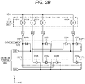
- Fig. 2B is a circuit diagram of the SMD 12.
- the SMD 12 includes a pixel (first pixel) 21P1, a pixel (first pixel) 21P2, a pixel (second pixel) 22P1, and a pixel (second pixel) 22P2.
- the pixel 21P1 and the pixel 21P2 have the same combination of colors of light emitting diode elements.
- the pixel 22P1 and the pixel 22P2 have the same combination of colors of light emitting diode elements.
- the pixels 21P1 and 21P2 and the pixels 22P1 and 22P2 have different combinations of colors of light emitting diode elements.
- the pixel 21P1 and the pixel 21P2 may be referred to as a pixel 21P.
- the pixel 22P1 and the pixel 22P2 may be referred to as a pixel 22P.
- the pixel 21P1 and the pixel 21P2 include a green LED element (first LED element) 20G and a red LED element (second LED element) 20R as a set of LED elements having different colors.
- the pixel 22P1 and the pixel 22P2 include a green LED element (third LED element) 20G and a blue LED element (fourth LED element) 20B as a set of LED elements having different colors.
- the pixels 21P and the pixels 22P are two-dimensionally arranged in a lattice shape (matrix shape) so as to be alternately arranged in the X-axis direction and alternately arranged in the Y-axis direction orthogonal to and intersecting the X-axis direction. That is, the pixels 21P and the pixels 22P are two-dimensionally arranged in a staggered manner. While Figs. 1 and 2A illustrate an example in which a basic lattice L in the arrangement in a lattice shape is a square, the shape of the basic lattice L is not limited thereto, and may be a quadrangle such as a rectangle, a rhombus, or a parallelogram.
- the SMD 12 includes one basic lattice L.
- the SMD 12 is of a cathode common type in which the cathode is a common terminal.
- the SMD 12 includes cathode terminals (gate terminals) 24GT1 and 24GT2 which are common terminals, an anode terminal 24R1, anode terminals 24G1 and 24G2, and an anode terminal 24B1.
- the cathodes of the green LED element 20G and the red LED element 20R included in the pixel 21P1 and the cathodes of the green LED element 20G and the blue LED element 20B included in the pixel 22P1 are connected to a scanning line GT1 via the common cathode terminal 24GT1.
- the cathodes of the green LED element 20G and the red LED element 20R included in the pixel 21P2 and the cathodes of the green LED element 20G and the blue LED element 20B included in the pixel 22P2 are connected to a scanning line GT2 via the common cathode terminal 24GT2.
- the anode of the green LED element 20G included in the pixel 21P1 and the anode of the green LED element 20G included in the pixel 22P2 are connected to a signal line G1 via the anode terminal 24G1.
- the anode of the green LED element 20G included in the pixel 21P2 and the anode of the green LED element 20G included in the pixel 22P1 are connected to a signal line G2 via the anode terminal 24G2.
- the anode of the red LED element 20R included in the pixel 21P1 and the anode of the red LED element 20R included in the pixel 21P2 are connected to a signal line R1 via the anode terminal 24R1.
- the anode of the blue LED element 20B included in the pixel 22P1 and the anode of the blue LED element 20B included in the pixel 22P2 are connected to a signal line B1 via the anode terminal 24B1.
- the scanning lines GT1 and GT2 are connected to gates (not illustrated) as switches.
- the signal lines R1, B1, G1, and G2 are connected to DC sources DC1, DC2, DC3, and DC4, respectively.
- a current flows from the driver into each of the LED elements 20R, 20G, and 20B.
- the display device 10 includes the plurality of pixels 21P including the green LED element 20G and the red LED element 20R, and the plurality of pixels 22P including the green LED element 20G and the blue LED element 20B.
- the pixels 21P and the pixels 22P are alternately arranged in the X-axis direction and alternately arranged in the Y-axis direction orthogonal to and intersecting the X-axis direction.
- the display device 10 since the number of LED elements can be reduced, the number of components of the display device 10 can be reduced. Hence, the reliability of the display device 10 can be improved. Furthermore, manufacturing can be simplified by changing the pixel configuration.
- the display device 10 since the number of driving wirings can be reduced, the wiring rule of the substrate 11 can be relaxed, and the number of driver ICs can be reduced.
- the cost of the display device 10 can be reduced.
- the amount of heat generation (i.e., power consumption) of the display device 10 can be reduced, and the luminance of the display device 10 can be improved.
- the pixels 21P1 and 21P2 are formed by thinning out the blue LED element 20B from the pixel having the LED elements 20R, 20G, and 20B of three colors
- the pixels 22P1 and 22P2 are formed by thinning out the red LED element 20R from the pixel having the LED elements 20R, 20G, and 20B of three colors
- the total signal amount can be reduced to 2/3. This is equivalent to Y chrominance conversion of a video signal (RGB).
- RGB video signal transmission, signal processing, and the like
- the cost of the circuit can be reduced.
- it is also possible to extend the signal transmission distance between the controller and the display unit since a reduction in the total amount of signals can curb deterioration in signal quality.
- both the pixel 21P and the pixel 22P have the green LED element 20G having high visibility, it is possible to curb degradation in the sense of resolution (image quality) even in a screen formed by two-dimensionally arranging a plurality of pixels 21P having only the LED elements 20G and 20R of two colors and a plurality of pixels 22P having only the LED elements 20G and 20B of two colors.
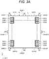
- Fig. 3A is a plan view of an SMD 32 of a comparative example.
- Fig. 3B is a circuit diagram of the SMD 32 of the comparative example.
- each of pixels 21P1, 21P2, 22P1, and 22P2 of the SMD 32 includes three LED elements 20R, 20G, and 20B of red, green, and blue. Therefore, as illustrated in Fig. 3B , the number of driving wirings is large, and the wiring rule of the substrate becomes complicated. Hence, the number of driver ICs increases.
- each of pixels 22P1 and 22P2 may include a yellow LED element (third LED element) 20Y instead of the green LED element (third LED element) 20G (see Figs. 2A and 2B ). That is, each of the pixels 22P1 and 22P2 may include the yellow LED element 20Y and a blue LED element 20B.
- an SMD 12 includes an anode terminal 24Y1 instead of the anode terminal 24G2 (see Fig. 2A ).
- the anode of the yellow LED element 20Y included in the pixel 22P1 is connected to a signal line Y1 via an anode terminal 24Y1, and the cathode of the yellow LED element 20Y is connected to a scanning line GT1 via a cathode terminal 24GT1.
- the anode of the yellow LED element 20Y included in the pixel 22P2 is connected to the signal line Y1 via the anode terminal 24Y1, and the cathode of the yellow LED element 20Y is connected to a scanning line GT2 via a cathode terminal 24GT2.
- Each of pixels 21P1 and 21P2 has the green LED element 20G having high visibility
- each of the pixels 22P1 and 22P2 has the yellow LED element 20Y having high visibility.
- yellow is a mixture of green and red
- the pixels 22P1 and 22P2 emit light close to white, and the sense of resolution is enhanced.
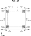
- each of pixels 22P1 and 22P2 may include a white LED element (third LED element) 20W instead of the green LED element (third LED element) 20G (see Figs. 2A and 2B ). That is, each of the pixels 22P1 and 22P2 may include the white LED element 20W and a blue LED element 20B.
- an SMD 12 includes an anode terminal 24W1 instead of the anode terminal 24G2 (see Fig. 2A ).
- the anode of the white LED element 20W included in the pixel 22P1 is connected to a signal line W1 via an anode terminal 24W1, and the cathode of the white LED element 20W is connected to a scanning line GT1 via a cathode terminal 24GT1.
- the anode of the white LED element 20W included in the pixel 22P2 is connected to the signal line W1 via the anode terminal 24W1, and the cathode of the white LED element 20W is connected to a scanning line GT2 via a cathode terminal 24GT2.
- the pixels 21P1 and 21P2 have the green LED element 20G having high visibility, and the pixels 22P1 and 22P2 have the white LED element 20W having high visibility.
- white is a mixture of green, red, and blue
- the pixels 22P1 and 22P2 emit light close to white, and the sense of resolution is enhanced.
- each of pixels 22P1 and 22P2 may further include a red LED element (fifth LED element) 20R in addition to the green LED element 20G and the blue LED element 20B (see Figs. 2A and 2B ).
- an SMD 12 further includes an anode terminal 24R2 in addition to cathode terminals 24GT1 and 24GT2, an anode terminal 24R1, anode terminals 24G1 and 24G2, and an anode terminal 24B1 (see Fig. 2A ).
- the anode of the added red LED element 20R included in the pixel 22P1 is connected to a signal line R2 via the anode terminal 24R2, and the cathode of the red LED element 20R is connected to a scanning line GT1 via the cathode terminal 24GT1.
- the anode of the added red LED element 20R included in the pixel 22P2 is connected to a signal line R1 via the anode terminal 24R1, and the cathode of the red LED element 20R is connected to a scanning line GT2 via the cathode terminal 24GT2.
- the anode of the red LED element 20R included in the pixel 21P2 is connected to the signal line R1 via the anode terminal 24R1.
- the anode of the red LED element 20R is connected to the signal line R2 via the anode terminal 24R2.
- An SMD 12 may have a circuit configuration different from that of Modification 3.
- red LED elements 20R included in pixels 21P1 and 22P2 adjacent in the Y-axis direction may be connected in parallel between a signal line R1 and a scanning line GT1.
- the anodes of the red LED elements 20R included in the pixels 21P1 and 22P2 adjacent in the Y-axis direction may both be connected to the signal line R1 via an anode terminal 24R1
- the cathodes of the red LED elements 20R may both be connected to the scanning line GT1 via a cathode terminal 24GT1.
- the red LED elements 20R included in pixels 22P1 and 21P2 adjacent in the Y-axis direction may be connected in parallel between the signal line R1 and a scanning line GT2.
- the anodes of the red LED elements 20R included in the pixels 22P1 and 21P2 adjacent in the Y-axis direction may both be connected to the signal line R1 via the anode terminal 24R1
- the cathodes of the red LED elements 20R may both be connected to the scanning line GT2 via a cathode terminal 24GT2.
- the SMD 12 has the above-described circuit configuration, as illustrated in Figs. 7A and 7B , the anode terminal 24R2 (see Fig. 6A ) and the signal line R2 (see Fig. 6B ) can be omitted.
- the SMD 12 is of a cathode common type in which the cathode is a common terminal.
- the SMD 12 may be of an anode common type in which the anode is a common terminal.
- the gate (switch) is provided on the common anode side of each of LED elements 20R, 20G, and 20B, switching is performed on the power supply side (high potential side), and a current is drawn from each of the LED elements 20R, 20G, and 20B by a current source on the cathode side.
- Fig. 8A is a plan view of an anode common type SMD 12.
- Fig. 8B is a circuit diagram of the anode common type SMD 12.
- the anode common type SMD 12 has anode terminals (gate terminals) 25GT1 and 25GT2 which are common terminals, a cathode terminal 25R1, cathode terminals 25G1 and G2, and a cathode terminal 25B1.
- the anodes of the green LED element 20G and the red LED element 20R included in a pixel 21P1 and the anodes of the green LED element 20G and the blue LED element 20B included in a pixel 22P1 are connected to a scanning line GT1 via the common anode terminal 25GT1.
- the anodes of the green LED element 20G and the red LED element 20R included in a pixel 21P2 and the anodes of the green LED element 20G and the blue LED element 20B included in a pixel 22P2 are connected to a scanning line GT2 via the common anode terminal 25GT2.
- the cathode of the green LED element 20G included in the pixel 21P1 and the cathode of the green LED element 20G included in the pixel 22P2 are connected to a signal line G1 via the cathode terminal 25G1.
- the green LED element 20G of the pixel 21P2 and the cathode of the green LED element 20G of the pixel 22P1 are connected to a signal line G2 via the cathode terminal 25G2.
- the cathode of the red LED element 20R included in the pixel 21P1 and the cathode of the red LED element 20R included in the pixel 21P2 are connected to a signal line R1 via the cathode terminal 25R1.
- the cathode of the blue LED element 20B included in the pixel 22P1 and the cathode of the blue LED element 20B included in the pixel 22P2 are connected to a signal line B1 via the cathode terminal 25B1.
- the scanning lines GT1 and GT2 are connected to gates (not illustrated) as switches.
- the signal lines R1, B1, G1, and G2 are connected to DC sources DC1, DC2, DC3, and DC4, respectively.
- the SMD 12 may be an anode common type instead of the cathode common type.
- each of the plurality of SMDs 12 includes 2 ⁇ 2 of the pixels 21P1 and 21P2.
- each of the plurality of SMDs 12 may include n ⁇ m of the pixels 21P1 and 21P2 (where n and m are, for example, an integer of 1 or more, preferably an integer of 2 or more, n is the number of pixels in the X-axis direction, and m is the number of pixels in the Y-axis direction.).
- the pixel arrangement in the first embodiment corresponds to an example in which each of the number n of pixels in the X-axis direction and the number m of pixels in the Y-axis direction is two.
- Fig. 9 is a plan view of a display device 110 according to a second embodiment of the present disclosure.
- the display device 110 includes a substrate 111, and a plurality of SMDs 121 and a plurality of SMDs 122 provided on the substrate 111.
- the substrate 111 is similar to the substrate 11 in the first embodiment except that it includes a plurality of SMDs 121 and a plurality of signal lines, a plurality of scanning lines and driver ICs, and the like for controlling the plurality of SMDs 122.
- the plurality of SMDs 121 and the plurality of SMDs 122 are two-dimensionally arranged in a lattice shape (matrix shape) such that the SMDs 121 and 122 are alternately arranged in the X-axis direction and alternately arranged in the Y-axis direction.
- the SMDs 121 and 122 are SMDs (1 in 1 SMD) in which one pixel is integrated into one chip.
- the positions of the plurality of SMDs 121 and 122 two-dimensionally arranged in a lattice shape are represented by (N, M) (where N indicates the numbers of the columns of the SMDs 121 and 122, and M indicates the numbers of the rows of the SMDs 121 and 122.).
- Fig. 10A is a plan view of the SMDs 121 and 122.
- Fig. 10B is a circuit diagram of the SMDs 121 and 122.
- the SMDs 121 and 122 are of a cathode common type in which the cathode is a common terminal.
- Each of the plurality of SMDs 121 includes one pixel (first pixel) 21P1.
- Each of the plurality of SMDs 122 includes one pixel (second pixel) 22P1.
- the SMD 121 includes a cathode terminal (gate terminal) 24GT, an anode terminal 24R, and an anode terminal 24G.
- the SMD 122 includes the cathode terminal (gate terminal) 24GT, an anode terminal 24B, and the anode terminal 24G.
- the cathodes of a green LED element 20G and a red LED element 20R included in the SMD 121 are connected to a scanning line GT1 via the common cathode terminal 24GT.
- the cathodes of the green LED element 20G and a blue LED element 20B included in the SMD 122 are connected to the scanning line GT1 via the common cathode terminal 24GT.
- the cathodes of the green LED element 20G and the red LED element 20R included in the SMD 121 are connected to a scanning line GT2 via the common cathode terminal 24GT.
- the cathodes of the green LED element 20G and the blue LED element 20B included in the SMD 122 are connected to the scanning line GT2 via the common cathode terminal 24GT.
- the anode of the green LED element 20G included in the SMD 121 (i.e., pixel 21P1) located at (N, M + 1) is connected to a signal line G1 via the anode terminal 24G.
- the anode of the red LED element 20R included in the SMD 121 (i.e., pixel 21P1) located at (N, M + 1) is connected to a signal line R1 via the anode terminal 24R.
- the anode of the green LED element 20G included in the SMD 122 (i.e., pixel 22P1) located at (N + 1, M + 1) is connected to a signal line G2 via the anode terminal 24G.
- the anode of the blue LED element 20B included in the SMD 122 (i.e., pixel 22P1) located at (N + 1, M + 1) is connected to a signal line B1 via the anode terminal 24B.
- the anode of the green LED element 20G included in the SMD 121 (i.e., pixel 21P1) located at (N + 1, M) is connected to the signal line G2 via the anode terminal 24G.
- the anode of the red LED element 20R included in the SMD 121 (i.e., pixel 21P1) located at (N + 1, M) is connected to the signal line R1 via the anode terminal 24R.
- the anode of the green LED element 20G included in the SMD 122 (i.e., pixel 22P1) located at (N, M) is connected to the signal line G1 via the anode terminal 24G.
- the anode of the blue LED element 20B included in the SMD 122 (i.e., pixel 22P1) located at (N, M) is connected to the signal line B1 via the anode terminal 24B.
- the display device 110 includes the plurality of SMDs 121 each having one pixel 21P1 and the plurality of SMDs 122 each having one pixel 22P1, and the SMDs 121 and 122 are alternately arranged in the X-axis direction and alternately arranged in the Y-axis direction. Therefore, an operation and effect similar to that of the display device 10 according to the first embodiment can be obtained.
- the above second embodiment describes an example in which the display device 110 includes the four pixels 21P1, 21P2, 22P1, and 22P2, which are included in one SMD 12 (see Fig. 2A ) in the first embodiment, in four separate SMDs 121 and 122.
- the four pixels 21P1, 21P2, 22P1, and 22P2 included in one SMD 12 in Modification 1, Modification 2, Modification 3, or Modification 4 of the first embodiment may be included in four separate SMDs 121 and 122.
- the SMDs 121 and 122 are of the cathode common type.
- the SMDs 121 and 122 may be of an anode common type.
- Fig. 11 is a plan view of a display device 210 according to a third embodiment of the present disclosure.
- the display device 210 includes a substrate 211 and a plurality of SMDs 212 provided on the substrate 211.
- the substrate 211 is similar to the substrate 11 in the first embodiment except that it includes a plurality of signal lines, a plurality of scanning lines and driver ICs, and the like for controlling the plurality of SMDs 212.
- Fig. 12A is a plan view of the SMD 212.
- Fig. 12B is a circuit diagram of the SMD 112.
- the SMD 212 is different from the SMD 12 in the first embodiment in that each of a pixel 22P1 and a pixel 22P2 includes only a green LED element 20G, and that the SMD 212 further includes a blue LED 23B arranged in a central part of a basic lattice L.
- the anode of the blue LED 23B is connected to a signal line B1, and the cathode of the blue LED 23B is connected to a scanning line GT2.
- the display device 210 according to the third embodiment is similar to the display device 10 according to the first embodiment in points other than the above.
- the blue LED 23B is arranged in the central part of the basic lattice L.
- the number of blue LED elements 20B can be reduced as compared with the display device 10 according to the first embodiment. Therefore, the display device 210 can be reduced in cost.
- each of a pixel 22P1 and a pixel 22P2 of the SMD 212 may further include a red LED element 20R.
- the anode of the red LED element 20R included in the pixel 22P1 may be connected to a signal line R2 via an anode terminal 24R2, and the cathode of the red LED element 20R may be connected to a scanning line GT1 via a cathode terminal 24GT1.
- the anode of the red LED element 20R included in the pixel 22P2 may be connected to a signal line R1 via an anode terminal 24R1, and the cathode of the red LED element 20R may be connected to a scanning line GT2 via a cathode terminal 24GT2.
- the SMD 212 may have a circuit configuration different from the above-described circuit configuration ( Fig. 13B ).
- the red LED elements 20R included in the pixels 21P1 and 22P2 adjacent in the Y-axis direction may be connected in parallel between the signal line R1 and the scanning line GT1.
- the anodes of the red LED elements 20R included in the pixels 21P1 and 22P2 adjacent in the Y-axis direction may both be connected to the signal line R1 via an anode terminal 24R1
- the cathodes of the red LED elements 20R may both be connected to the scanning line GT1 via the cathode terminal 24GT1.
- the red LED elements 20R included in the pixels 22P1 and 21P2 adjacent in the Y-axis direction may be connected in parallel between the signal line R1 and the scanning line GT2.
- the anodes of the red LED elements 20R included in the pixels 22P1 and 21P2 adjacent in the Y-axis direction may both be connected to the signal line R1 via the anode terminal 24R1
- the cathodes of the red LED elements 20R may both be connected to the scanning line GT2 via the cathode terminal 24GT2.
- the SMD 212 has the above-described circuit configuration, the anode terminal 24R2 (see Fig. 13A ) and the signal line R2 (see Fig. 13B ) can be omitted.
- the display devices 10, 110, and 210 include the plurality of SMDs 12, 121, 122, and 212 having the plurality of LED elements 20R, 20B, and 20G
- a plurality of chip on boards (COBs) or glue on boards (GOBs) having the plurality of LED elements 20R, 20B, and 20G may be included.
- a GOB includes a protective layer covering a plurality of pixels 21P and a plurality of pixels 22P on a display surface.
- the protective layer includes a resin layer or a film, for example.
- the plurality of SMDs 12, 121, 122, and 212 is secondarily arranged on the substrate.
- the plurality of pixels 21P and the plurality of pixels 22P may be two-dimensionally arranged directly on the substrates 11, 111, and 211.
- the plurality of LED elements 20R, 20B, and 20G may be embedded in the substrates 11, 111, and 211.
- the LED elements 20R, 20B, and 20G may be micro LED elements.
- the pixels 21P1, 21P2, 22P1, and 22P2 include the red LED element 20R, the green LED element 20G, the blue LED element 20B, and the yellow LED element 20Y as light emitting units.
- the light emitting units are not limited thereto.
- the pixel 21P1 and the like may include, instead of the red LED element 20R, a white LED element 20W and a red filter provided on the white LED element 20W, and include a red light emitting unit capable of emitting red light.
- the pixel 21P1 and the like may include, instead of the green LED element 20G, a white LED element 20W and a green filter provided on the white LED element 20W, and include a green light emitting unit capable of emitting green light.
- the pixel 21P1 and the like may include, instead of the blue LED element 20B, a white LED element 20W and a blue filter provided on the white LED element 20W, and include a blue light emitting unit capable of emitting blue light.
- the pixel 21P1 and the like may include, instead of the yellow LED element 20Y, a white LED element 20W and a yellow filter provided on the white LED element 20W, and include a yellow light emitting unit capable of emitting yellow light.
- the SMD 212 may include a white LED element 20W and a blue filter provided on the white LED element 20W, and include a blue light emitting unit capable of emitting blue light.
- a light emitting unit may have the following configuration.
- the pixel 21P1 and the like may include a blue LED and a red light emitting element by quantum dot (QD) color conversion instead of the red LED element 20R.
- the pixel 21P1 and the like may include a blue LED and a green light emitting element by quantum dot (QD) color conversion instead of the green LED element 20G.
- the pixel 21P1 and the like may include a blue LED and a yellow light emitting element by quantum dot (QD) color conversion instead of the yellow LED element 20Y.
Landscapes
- Engineering & Computer Science (AREA)
- Physics & Mathematics (AREA)
- General Physics & Mathematics (AREA)
- Theoretical Computer Science (AREA)
- Computer Hardware Design (AREA)
- Led Device Packages (AREA)
- Devices For Indicating Variable Information By Combining Individual Elements (AREA)
Abstract
Description
- The present disclosure relates to a display device.
- In recent years, an LED display device in which a plurality of light emitting diode elements (hereinafter referred to as "LED elements") is two-dimensionally arranged has been widely known. In an LED display device, one pixel includes LEDs of three colors of red (R), green (G), and blue (B) (see
Patent Document 1, for example). - Patent Document 1:
Japanese Patent Application Laid-Open No. 2001-75508 - However, in the LED display device described above, since LED elements of three colors of R, G, and B are used, there is a problem that the number of wirings on the substrate increases. In particular, in a highresolution LED display device, since the number of LED elements increases, the problem of the number of wires becomes significant.
- An object of the present disclosure is to provide a display device capable of reducing the number of wirings on a substrate and simplifying manufacturing by changing the pixel configuration.
- In order to solve the above-described problem, a first disclosure provides a display device including:
- a plurality of first pixels each having a first light emitting diode element and a second light emitting diode element having different colors; and
- a plurality of second pixels each having a third light emitting diode element and a fourth light emitting diode element having different colors,
- in which the first pixels and the second pixels have different combinations of colors of light emitting diode elements,
- the first light emitting diode element is a green light emitting diode element,
- the third light emitting diode element is a green light emitting diode element, a yellow light emitting diode element, or a white light emitting diode element, and
- the first pixels and the second pixels are alternately arranged in a first direction and are alternately arranged in a second direction intersecting the first direction.
- According to a second disclosure, there is provided a display device including:
- a plurality of first pixels each having a green light emitting diode element and a red light emitting diode element;
- a plurality of second pixels each having a green light emitting diode element; and
- a blue light emitting diode element,
- in which the first pixels and the second pixels are arranged in a lattice shape so as to be alternately arranged in a first direction and alternately arranged in a second direction intersecting the first direction, and
- the blue light emitting diode element is arranged in a central part of a basic lattice in the arrangement in a lattice shape.
- According to a third disclosure, there is provided a display device including:
- a first pixel including a first light emitting unit and a second light emitting unit having different colors; and
- a second pixel including a third light emitting unit and a fourth light emitting unit having different colors,
- in which the first pixel and the second pixel have different combinations of colors of light emitting units,
- the first light emitting unit is a green light emitting unit including a white light emitting diode and a green filter,
- the third light emitting unit is a green light emitting unit including a white light emitting diode and a green filter, a yellow light emitting unit including a white light emitting diode and a yellow filter, or a white light emitting unit including a white light emitting diode, and
- the first pixel and the second pixel are alternately arranged in a first direction and are alternately arranged in a second direction intersecting the first direction.
- According to a fourth disclosure, there is provided a display device including:
- a plurality of first pixels each including a green light emitting unit and a red light emitting unit;
- a plurality of second pixels each including a green light emitting unit; and
- a blue light emitting unit,
- wherein the green light emitting unit included in the first pixel and the green light emitting unit included in the second pixel include a white light emitting diode and a green filter,
- the red light emitting unit includes a white light emitting diode and a red filter,
- the blue light emitting unit includes a white light emitting diode and a blue filter,
- the first pixels and the second pixels are arranged in a lattice shape so as to be alternately arranged in a first direction and alternately arranged in a second direction intersecting the first direction, and
- the blue light emitting unit is arranged in a central part of a basic lattice in the arrangement in a lattice shape.
-
-
Fig. 1 is a plan view of a display device according to a first embodiment of the present disclosure. -
Fig. 2A is a plan view of a surface mount device. -
Fig. 2B is a circuit diagram of the surface mount device. -
Fig. 3A is a plan view of a surface mount device of a comparative example. -
Fig. 3B is a circuit diagram of the surface mount device. -
Fig. 4A is a plan view of a surface mount device of a modification. -
Fig. 4B is a circuit diagram of the surface mount device of the modification. -
Fig. 5A is a plan view of a surface mount device of a modification. -
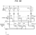
Fig. 5B is a circuit diagram of the surface mount device of the modification. -
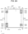
Fig. 6A is a plan view of a surface mount device of a modification. -
Fig. 6B is a circuit diagram of the surface mount device of the modification. -
Fig. 7A is a plan view of a surface mount device of a modification. -
Fig. 7B is a circuit diagram of the surface mount device of the modification. -
Fig. 8A is a plan view of a surface mount device of a modification. -
Fig. 8B is a circuit diagram of the surface mount device of the modification. -
Fig. 9 is a plan view of a display device according to a second embodiment of the present disclosure. -
Fig. 10A is a plan view of a surface mount device. -
Fig. 10B is a circuit diagram of the surface mount device. -
Fig. 11 is a plan view of a display device according to a third embodiment of the present disclosure. -
Fig. 12A is a plan view of a surface mount device. -
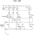
Fig. 12B is a circuit diagram of the surface mount device. -
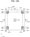
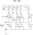
Fig. 13A is a plan view of a surface mount device of a modification. -
Fig. 13B is a circuit diagram of a surface mount device of a modification. -
Fig. 13C is a circuit diagram of a surface mount device of a modification. - Embodiments of the present disclosure will be described in the following order. Note that in all the drawings of the following embodiments, the same or corresponding parts are denoted by the same reference numerals.
- 1 First embodiment (example of display device in which plurality of surface mount devices having four pixels is arranged)
- 2 Second embodiment (example of display device in which plurality of surface mount devices having one pixel is arranged)
- 3 Third embodiment (example of display device in which plurality of surface mount devices having LED element in central part is arranged)
- Since the human eye has low resolution and recognition for the color blue (less M cones), the sense of resolution is not largely affected even if blue LED elements are thinned out from pixels having LED elements of three colors of red, green, and blue. Furthermore, since the resolution and recognition for the color red is less visible than the color green, the sense of resolution is not largely affected even if red LED elements are thinned out from pixels having LED elements of three colors.
- In the display device according to the first embodiment, a plurality of first pixels having LED elements of two colors of red and green and a plurality of second pixels having LED elements of two colors of green and blue are two-dimensionally arranged on the basis of the above viewpoint.
-
Fig. 1 is a plan view of adisplay device 10 according to a first embodiment of the present disclosure. Thedisplay device 10 is a so-called LED display device, and includes asubstrate 11 and a plurality of surface mount devices (hereinafter referred to as "SMDs") 12 provided on thesubstrate 11. - The
substrate 11 is, for example, a printed circuit board (PCB). A plurality of scanning lines, a plurality of signal lines, and driver integrated circuits (IC) for controlling the plurality ofSMDs 12 via the plurality of scanning lines and the plurality of signal lines are provided on thesubstrate 11. - The plurality of
SMDs 12 is two-dimensionally arranged in a lattice shape on thesubstrate 11. In the following description, a row direction of the twodimensional arrangement is referred to as an X-axis direction (first direction), and a column direction orthogonal to and intersecting the row direction is referred to as a Y-axis direction (second direction). TheSMD 12 is an SMD (4 in 1 SMD) in which four pixels are integrated into one chip. -
Fig. 2A is a plan view of theSMD 12.Fig. 2B is a circuit diagram of theSMD 12. TheSMD 12 includes a pixel (first pixel) 21P1, a pixel (first pixel) 21P2, a pixel (second pixel) 22P1, and a pixel (second pixel) 22P2. The pixel 21P1 and the pixel 21P2 have the same combination of colors of light emitting diode elements. The pixel 22P1 and the pixel 22P2 have the same combination of colors of light emitting diode elements. The pixels 21P1 and 21P2 and the pixels 22P1 and 22P2 have different combinations of colors of light emitting diode elements. In the following description, in a case where the pixel 21P1 and the pixel 21P2 are not particularly distinguished, the pixel 21P1 and the pixel 21P2 may be referred to as a pixel 21P. Furthermore, in a case where the pixel 22P1 and the pixel 22P2 are not particularly distinguished, the pixel 22P1 and the pixel 22P2 may be referred to as a pixel 22P. - The pixel 21P1 and the pixel 21P2 include a green LED element (first LED element) 20G and a red LED element (second LED element) 20R as a set of LED elements having different colors. The pixel 22P1 and the pixel 22P2 include a green LED element (third LED element) 20G and a blue LED element (fourth LED element) 20B as a set of LED elements having different colors.
- The pixels 21P and the pixels 22P are two-dimensionally arranged in a lattice shape (matrix shape) so as to be alternately arranged in the X-axis direction and alternately arranged in the Y-axis direction orthogonal to and intersecting the X-axis direction. That is, the pixels 21P and the pixels 22P are two-dimensionally arranged in a staggered manner. While
Figs. 1 and2A illustrate an example in which a basic lattice L in the arrangement in a lattice shape is a square, the shape of the basic lattice L is not limited thereto, and may be a quadrangle such as a rectangle, a rhombus, or a parallelogram. TheSMD 12 includes one basic lattice L. - The
SMD 12 is of a cathode common type in which the cathode is a common terminal. TheSMD 12 includes cathode terminals (gate terminals) 24GT1 and 24GT2 which are common terminals, an anode terminal 24R1, anode terminals 24G1 and 24G2, and an anode terminal 24B1. - The cathodes of the
green LED element 20G and thered LED element 20R included in the pixel 21P1 and the cathodes of thegreen LED element 20G and theblue LED element 20B included in the pixel 22P1 are connected to a scanning line GT1 via the common cathode terminal 24GT1. The cathodes of thegreen LED element 20G and thered LED element 20R included in the pixel 21P2 and the cathodes of thegreen LED element 20G and theblue LED element 20B included in the pixel 22P2 are connected to a scanning line GT2 via the common cathode terminal 24GT2. - The anode of the
green LED element 20G included in the pixel 21P1 and the anode of thegreen LED element 20G included in the pixel 22P2 are connected to a signal line G1 via the anode terminal 24G1. The anode of thegreen LED element 20G included in the pixel 21P2 and the anode of thegreen LED element 20G included in the pixel 22P1 are connected to a signal line G2 via the anode terminal 24G2. - The anode of the
red LED element 20R included in the pixel 21P1 and the anode of thered LED element 20R included in the pixel 21P2 are connected to a signal line R1 via the anode terminal 24R1. - The anode of the
blue LED element 20B included in the pixel 22P1 and the anode of theblue LED element 20B included in the pixel 22P2 are connected to a signal line B1 via the anode terminal 24B1. - The scanning lines GT1 and GT2 are connected to gates (not illustrated) as switches. The signal lines R1, B1, G1, and G2 are connected to DC sources DC1, DC2, DC3, and DC4, respectively. In the cathode
common type SMD 12, a current flows from the driver into each of theLED elements - As described above, the
display device 10 according to the first embodiment includes the plurality of pixels 21P including thegreen LED element 20G and thered LED element 20R, and the plurality of pixels 22P including thegreen LED element 20G and theblue LED element 20B. The pixels 21P and the pixels 22P are alternately arranged in the X-axis direction and alternately arranged in the Y-axis direction orthogonal to and intersecting the X-axis direction. - With the above configuration, in the
display device 10, since the number of LED elements can be reduced, the number of components of thedisplay device 10 can be reduced. Hence, the reliability of thedisplay device 10 can be improved. Furthermore, manufacturing can be simplified by changing the pixel configuration. - Furthermore, in the
display device 10, since the number of driving wirings can be reduced, the wiring rule of thesubstrate 11 can be relaxed, and the number of driver ICs can be reduced. - Furthermore, since the number of components and the driver ICs can be reduced as described above, the cost of the
display device 10 can be reduced. - Furthermore, by reducing the number of driver ICs described above, the amount of heat generation (i.e., power consumption) of the
display device 10 can be reduced, and the luminance of thedisplay device 10 can be improved. - Since the pixels 21P1 and 21P2 are formed by thinning out the
blue LED element 20B from the pixel having theLED elements red LED element 20R from the pixel having theLED elements - Since both the pixel 21P and the pixel 22P have the
green LED element 20G having high visibility, it is possible to curb degradation in the sense of resolution (image quality) even in a screen formed by two-dimensionally arranging a plurality of pixels 21P having only theLED elements LED elements -
Fig. 3A is a plan view of an SMD 32 of a comparative example.Fig. 3B is a circuit diagram of the SMD 32 of the comparative example. As illustrated inFig. 3A , each of pixels 21P1, 21P2, 22P1, and 22P2 of the SMD 32 includes threeLED elements Fig. 3B , the number of driving wirings is large, and the wiring rule of the substrate becomes complicated. Hence, the number of driver ICs increases. - As illustrated in
Figs. 4A and4B , each of pixels 22P1 and 22P2 may include a yellow LED element (third LED element) 20Y instead of the green LED element (third LED element) 20G (seeFigs. 2A and2B ). That is, each of the pixels 22P1 and 22P2 may include theyellow LED element 20Y and ablue LED element 20B. - In the case of the pixel configuration described above, an
SMD 12 includes an anode terminal 24Y1 instead of the anode terminal 24G2 (seeFig. 2A ). The anode of theyellow LED element 20Y included in the pixel 22P1 is connected to a signal line Y1 via an anode terminal 24Y1, and the cathode of theyellow LED element 20Y is connected to a scanning line GT1 via a cathode terminal 24GT1. The anode of theyellow LED element 20Y included in the pixel 22P2 is connected to the signal line Y1 via the anode terminal 24Y1, and the cathode of theyellow LED element 20Y is connected to a scanning line GT2 via a cathode terminal 24GT2. - Each of pixels 21P1 and 21P2 has the
green LED element 20G having high visibility, and each of the pixels 22P1 and 22P2 has theyellow LED element 20Y having high visibility. As a result, it is possible to curb degradation in the sense of resolution (image quality) even in a screen formed by two-dimensionally arranging the plurality of pixels 21P1 and 21P2 having only theLED elements LED elements - Furthermore, since yellow is a mixture of green and red, in a display state with low chroma such as a white display state, the pixels 22P1 and 22P2 emit light close to white, and the sense of resolution is enhanced.
- As illustrated in
Figs. 5A and5B , each of pixels 22P1 and 22P2 may include a white LED element (third LED element) 20W instead of the green LED element (third LED element) 20G (seeFigs. 2A and2B ). That is, each of the pixels 22P1 and 22P2 may include thewhite LED element 20W and ablue LED element 20B. - In the case of the pixel configuration described above, an
SMD 12 includes an anode terminal 24W1 instead of the anode terminal 24G2 (seeFig. 2A ). The anode of thewhite LED element 20W included in the pixel 22P1 is connected to a signal line W1 via an anode terminal 24W1, and the cathode of thewhite LED element 20W is connected to a scanning line GT1 via a cathode terminal 24GT1. The anode of thewhite LED element 20W included in the pixel 22P2 is connected to the signal line W1 via the anode terminal 24W1, and the cathode of thewhite LED element 20W is connected to a scanning line GT2 via a cathode terminal 24GT2. - The pixels 21P1 and 21P2 have the
green LED element 20G having high visibility, and the pixels 22P1 and 22P2 have thewhite LED element 20W having high visibility. As a result, it is possible to curb degradation in the sense of resolution (image quality) even in a screen formed by two-dimensionally arranging the plurality of pixels 21P1 and 21P2 having only theLED elements LED elements - Furthermore, since white is a mixture of green, red, and blue, in a display state with low chroma such as a white display state, the pixels 22P1 and 22P2 emit light close to white, and the sense of resolution is enhanced.
- As illustrated in
Figs. 6A and6B , each of pixels 22P1 and 22P2 may further include a red LED element (fifth LED element) 20R in addition to thegreen LED element 20G and theblue LED element 20B (seeFigs. 2A and2B ). - In the case of the above configuration, an
SMD 12 further includes an anode terminal 24R2 in addition to cathode terminals 24GT1 and 24GT2, an anode terminal 24R1, anode terminals 24G1 and 24G2, and an anode terminal 24B1 (seeFig. 2A ). The anode of the addedred LED element 20R included in the pixel 22P1 is connected to a signal line R2 via the anode terminal 24R2, and the cathode of thered LED element 20R is connected to a scanning line GT1 via the cathode terminal 24GT1. The anode of the addedred LED element 20R included in the pixel 22P2 is connected to a signal line R1 via the anode terminal 24R1, and the cathode of thered LED element 20R is connected to a scanning line GT2 via the cathode terminal 24GT2. In the first embodiment, the anode of thered LED element 20R included in the pixel 21P2 is connected to the signal line R1 via the anode terminal 24R1. However, inModification 3, the anode of thered LED element 20R is connected to the signal line R2 via the anode terminal 24R2. - An
SMD 12 may have a circuit configuration different from that ofModification 3. For example, as illustrated inFig. 7B , in theSMD 12,red LED elements 20R included in pixels 21P1 and 22P2 adjacent in the Y-axis direction may be connected in parallel between a signal line R1 and a scanning line GT1. Specifically, the anodes of thered LED elements 20R included in the pixels 21P1 and 22P2 adjacent in the Y-axis direction may both be connected to the signal line R1 via an anode terminal 24R1, and the cathodes of thered LED elements 20R may both be connected to the scanning line GT1 via a cathode terminal 24GT1. - Similarly, the
red LED elements 20R included in pixels 22P1 and 21P2 adjacent in the Y-axis direction may be connected in parallel between the signal line R1 and a scanning line GT2. Specifically, the anodes of thered LED elements 20R included in the pixels 22P1 and 21P2 adjacent in the Y-axis direction may both be connected to the signal line R1 via the anode terminal 24R1, and the cathodes of thered LED elements 20R may both be connected to the scanning line GT2 via a cathode terminal 24GT2. - Since the
SMD 12 has the above-described circuit configuration, as illustrated inFigs. 7A and7B , the anode terminal 24R2 (seeFig. 6A ) and the signal line R2 (seeFig. 6B ) can be omitted. - In the first embodiment, an example in which the
SMD 12 is of a cathode common type in which the cathode is a common terminal has been described. However, theSMD 12 may be of an anode common type in which the anode is a common terminal. In an anodecommon type SMD 12, the gate (switch) is provided on the common anode side of each ofLED elements LED elements -
Fig. 8A is a plan view of an anodecommon type SMD 12.Fig. 8B is a circuit diagram of the anodecommon type SMD 12. The anodecommon type SMD 12 has anode terminals (gate terminals) 25GT1 and 25GT2 which are common terminals, a cathode terminal 25R1, cathode terminals 25G1 and G2, and a cathode terminal 25B1. - The anodes of the
green LED element 20G and thered LED element 20R included in a pixel 21P1 and the anodes of thegreen LED element 20G and theblue LED element 20B included in a pixel 22P1 are connected to a scanning line GT1 via the common anode terminal 25GT1. The anodes of thegreen LED element 20G and thered LED element 20R included in a pixel 21P2 and the anodes of thegreen LED element 20G and theblue LED element 20B included in a pixel 22P2 are connected to a scanning line GT2 via the common anode terminal 25GT2. - The cathode of the
green LED element 20G included in the pixel 21P1 and the cathode of thegreen LED element 20G included in the pixel 22P2 are connected to a signal line G1 via the cathode terminal 25G1. Thegreen LED element 20G of the pixel 21P2 and the cathode of thegreen LED element 20G of the pixel 22P1 are connected to a signal line G2 via the cathode terminal 25G2. - The cathode of the
red LED element 20R included in the pixel 21P1 and the cathode of thered LED element 20R included in the pixel 21P2 are connected to a signal line R1 via the cathode terminal 25R1. - The cathode of the
blue LED element 20B included in the pixel 22P1 and the cathode of theblue LED element 20B included in the pixel 22P2 are connected to a signal line B1 via the cathode terminal 25B1. - The scanning lines GT1 and GT2 are connected to gates (not illustrated) as switches. The signal lines R1, B1, G1, and G2 are connected to DC sources DC1, DC2, DC3, and DC4, respectively.
- Note that in
Modifications 1 to 4, too, theSMD 12 may be an anode common type instead of the cathode common type. - In the first embodiment, an example has been described in which each of the plurality of
SMDs 12 includes 2 × 2 of the pixels 21P1 and 21P2. However, each of the plurality ofSMDs 12 may include n × m of the pixels 21P1 and 21P2 (where n and m are, for example, an integer of 1 or more, preferably an integer of 2 or more, n is the number of pixels in the X-axis direction, and m is the number of pixels in the Y-axis direction.). Note that the pixel arrangement in the first embodiment corresponds to an example in which each of the number n of pixels in the X-axis direction and the number m of pixels in the Y-axis direction is two. -
Fig. 9 is a plan view of adisplay device 110 according to a second embodiment of the present disclosure. Thedisplay device 110 includes asubstrate 111, and a plurality ofSMDs 121 and a plurality ofSMDs 122 provided on thesubstrate 111. - The
substrate 111 is similar to thesubstrate 11 in the first embodiment except that it includes a plurality ofSMDs 121 and a plurality of signal lines, a plurality of scanning lines and driver ICs, and the like for controlling the plurality ofSMDs 122. - The plurality of
SMDs 121 and the plurality ofSMDs 122 are two-dimensionally arranged in a lattice shape (matrix shape) such that theSMDs SMDs SMDs SMDs SMDs -
Fig. 10A is a plan view of theSMDs Fig. 10B is a circuit diagram of theSMDs SMDs SMDs 121 includes one pixel (first pixel) 21P1. Each of the plurality ofSMDs 122 includes one pixel (second pixel) 22P1. TheSMD 121 includes a cathode terminal (gate terminal) 24GT, ananode terminal 24R, and ananode terminal 24G. TheSMD 122 includes the cathode terminal (gate terminal) 24GT, ananode terminal 24B, and theanode terminal 24G. - The cathodes of a
green LED element 20G and ared LED element 20R included in the SMD 121 (i.e., pixel 21P1) located at (N, M + 1) are connected to a scanning line GT1 via the common cathode terminal 24GT. The cathodes of thegreen LED element 20G and ablue LED element 20B included in the SMD 122 (i.e., pixel 22P1) located at (N + 1, M + 1) are connected to the scanning line GT1 via the common cathode terminal 24GT. - The cathodes of the
green LED element 20G and thered LED element 20R included in the SMD 121 (i.e., pixel 21P1) located at (N + 1, M) are connected to a scanning line GT2 via the common cathode terminal 24GT. The cathodes of thegreen LED element 20G and theblue LED element 20B included in the SMD 122 (i.e., pixel 22P1) located at (N, M) are connected to the scanning line GT2 via the common cathode terminal 24GT. - The anode of the
green LED element 20G included in the SMD 121 (i.e., pixel 21P1) located at (N, M + 1) is connected to a signal line G1 via theanode terminal 24G. The anode of thered LED element 20R included in the SMD 121 (i.e., pixel 21P1) located at (N, M + 1) is connected to a signal line R1 via theanode terminal 24R. - The anode of the
green LED element 20G included in the SMD 122 (i.e., pixel 22P1) located at (N + 1, M + 1) is connected to a signal line G2 via theanode terminal 24G. The anode of theblue LED element 20B included in the SMD 122 (i.e., pixel 22P1) located at (N + 1, M + 1) is connected to a signal line B1 via theanode terminal 24B. - The anode of the
green LED element 20G included in the SMD 121 (i.e., pixel 21P1) located at (N + 1, M) is connected to the signal line G2 via theanode terminal 24G. The anode of thered LED element 20R included in the SMD 121 (i.e., pixel 21P1) located at (N + 1, M) is connected to the signal line R1 via theanode terminal 24R. - The anode of the
green LED element 20G included in the SMD 122 (i.e., pixel 22P1) located at (N, M) is connected to the signal line G1 via theanode terminal 24G. The anode of theblue LED element 20B included in the SMD 122 (i.e., pixel 22P1) located at (N, M) is connected to the signal line B1 via theanode terminal 24B. - As described above, the
display device 110 according to the second embodiment includes the plurality ofSMDs 121 each having one pixel 21P1 and the plurality ofSMDs 122 each having one pixel 22P1, and theSMDs display device 10 according to the first embodiment can be obtained. - The above second embodiment describes an example in which the
display device 110 includes the four pixels 21P1, 21P2, 22P1, and 22P2, which are included in one SMD 12 (seeFig. 2A ) in the first embodiment, in fourseparate SMDs SMD 12 inModification 1,Modification 2,Modification 3, orModification 4 of the first embodiment may be included in fourseparate SMDs - In the second embodiment, an example in which the
SMDs SMDs -
Fig. 11 is a plan view of adisplay device 210 according to a third embodiment of the present disclosure. Thedisplay device 210 includes asubstrate 211 and a plurality ofSMDs 212 provided on thesubstrate 211. - The
substrate 211 is similar to thesubstrate 11 in the first embodiment except that it includes a plurality of signal lines, a plurality of scanning lines and driver ICs, and the like for controlling the plurality ofSMDs 212. -
Fig. 12A is a plan view of theSMD 212.Fig. 12B is a circuit diagram of the SMD 112. TheSMD 212 is different from theSMD 12 in the first embodiment in that each of a pixel 22P1 and a pixel 22P2 includes only agreen LED element 20G, and that theSMD 212 further includes ablue LED 23B arranged in a central part of a basic lattice L. The anode of theblue LED 23B is connected to a signal line B1, and the cathode of theblue LED 23B is connected to a scanning line GT2. - The
display device 210 according to the third embodiment is similar to thedisplay device 10 according to the first embodiment in points other than the above. - As described above, in the
display device 210 according to the third embodiment, instead of providing theblue LED element 20B to each of the pixels 22P1 and 22P2, theblue LED 23B is arranged in the central part of the basic lattice L. As a result, the number ofblue LED elements 20B can be reduced as compared with thedisplay device 10 according to the first embodiment. Therefore, thedisplay device 210 can be reduced in cost. - In the above-described third embodiment, an example in which the pixel 22P1 and the pixel 22P2 of the
SMD 212 each include only thegreen LED element 20G has been described. However, as illustrated inFig. 13A , each of a pixel 22P1 and a pixel 22P2 may further include ared LED element 20R. - In a case where an
SMD 212 has the above-described pixel configuration, as illustrated inFig. 13B , the anode of thered LED element 20R included in the pixel 22P1 may be connected to a signal line R2 via an anode terminal 24R2, and the cathode of thered LED element 20R may be connected to a scanning line GT1 via a cathode terminal 24GT1. The anode of thered LED element 20R included in the pixel 22P2 may be connected to a signal line R1 via an anode terminal 24R1, and the cathode of thered LED element 20R may be connected to a scanning line GT2 via a cathode terminal 24GT2. - The
SMD 212 may have a circuit configuration different from the above-described circuit configuration (Fig. 13B ). For example, as illustrated inFig. 13C , in theSMD 212, thered LED elements 20R included in the pixels 21P1 and 22P2 adjacent in the Y-axis direction may be connected in parallel between the signal line R1 and the scanning line GT1. Specifically, the anodes of thered LED elements 20R included in the pixels 21P1 and 22P2 adjacent in the Y-axis direction may both be connected to the signal line R1 via an anode terminal 24R1, and the cathodes of thered LED elements 20R may both be connected to the scanning line GT1 via the cathode terminal 24GT1. - Similarly, the
red LED elements 20R included in the pixels 22P1 and 21P2 adjacent in the Y-axis direction may be connected in parallel between the signal line R1 and the scanning line GT2. Specifically, the anodes of thered LED elements 20R included in the pixels 22P1 and 21P2 adjacent in the Y-axis direction may both be connected to the signal line R1 via the anode terminal 24R1, and the cathodes of thered LED elements 20R may both be connected to the scanning line GT2 via the cathode terminal 24GT2. - Since the
SMD 212 has the above-described circuit configuration, the anode terminal 24R2 (seeFig. 13A ) and the signal line R2 (seeFig. 13B ) can be omitted. - In the above-described first to third embodiments, an example in which the
display devices SMDs LED elements SMDs LED elements - In the above-described first to third embodiments, an example in which the plurality of
SMDs substrates LED elements substrates LED elements - In the first to third embodiments described above, an example has been described in which the pixels 21P1, 21P2, 22P1, and 22P2 (hereinafter referred to as pixel 21P1 and the like) include the
red LED element 20R, thegreen LED element 20G, theblue LED element 20B, and theyellow LED element 20Y as light emitting units. However, the light emitting units are not limited thereto. For example, the pixel 21P1 and the like may include, instead of thered LED element 20R, awhite LED element 20W and a red filter provided on thewhite LED element 20W, and include a red light emitting unit capable of emitting red light. The pixel 21P1 and the like may include, instead of thegreen LED element 20G, awhite LED element 20W and a green filter provided on thewhite LED element 20W, and include a green light emitting unit capable of emitting green light. The pixel 21P1 and the like may include, instead of theblue LED element 20B, awhite LED element 20W and a blue filter provided on thewhite LED element 20W, and include a blue light emitting unit capable of emitting blue light. The pixel 21P1 and the like may include, instead of theyellow LED element 20Y, awhite LED element 20W and a yellow filter provided on thewhite LED element 20W, and include a yellow light emitting unit capable of emitting yellow light. - Furthermore, in the third embodiment, instead of the
blue LED 23B, theSMD 212 may include awhite LED element 20W and a blue filter provided on thewhite LED element 20W, and include a blue light emitting unit capable of emitting blue light. - Furthermore, a light emitting unit may have the following configuration. For example, the pixel 21P1 and the like may include a blue LED and a red light emitting element by quantum dot (QD) color conversion instead of the
red LED element 20R. The pixel 21P1 and the like may include a blue LED and a green light emitting element by quantum dot (QD) color conversion instead of thegreen LED element 20G. The pixel 21P1 and the like may include a blue LED and a yellow light emitting element by quantum dot (QD) color conversion instead of theyellow LED element 20Y. - While embodiments and modifications of the present disclosure have been specifically described above, the present disclosure is not limited to the above-described embodiments and modifications, and various modifications based on the technical idea of the present disclosure are possible.
- For example, the configurations, methods, shapes, and the like described in the above embodiments and modifications are merely examples, and different configurations, methods, shapes, and the like may be used as necessary.
- The configurations, methods, shapes, and the like of the above-described embodiments and modifications can be combined with each other without departing from the gist of the present disclosure.
- Furthermore, the present disclosure can adopt the following configurations.
- (1) A display device including:
- a plurality of first pixels each having a first light emitting diode element and a second light emitting diode element having different colors; and
- a plurality of second pixels each having a third light emitting diode element and a fourth light emitting diode element having different colors, in which
- the first pixels and the second pixels have different combinations of colors of light emitting diode elements,
- the first light emitting diode element is a green light emitting diode element,
- the third light emitting diode element is a green light emitting diode element, a yellow light emitting diode element, or a white light emitting diode element, and
- the first pixels and the second pixels are alternately arranged in a first direction and are alternately arranged in a second direction intersecting the first direction.
- (2) The display device according to (1), in which
- the second light emitting diode element is a red light emitting diode element,
- the third light emitting diode element is the green light emitting diode element, and
- the fourth light emitting diode element is a blue light emitting diode element.
- (3) The display device according to (1), in which
- the second light emitting diode element is a red light emitting diode element,
- the third light emitting diode element is the yellow light emitting diode element, and
- the fourth light emitting diode element is a blue light emitting diode element.
- (4) The display device according to (1), in which
- the second light emitting diode element is a red light emitting diode element,
- the third light emitting diode element is the white light emitting diode element, and
- the fourth light emitting diode element is a blue light emitting diode element.
- (5) The display device according to (1), in which
- the second pixel further includes a fifth light emitting diode element,
- the second light emitting diode element is a red light emitting diode element,
- the third light emitting diode element is the green light emitting diode element,
- the fourth light emitting diode element is a blue light emitting diode element, and
- the fifth light emitting diode element is a red light emitting diode element.
- (6) The display device according to (5), in which the red light emitting diode elements that are included in the first pixel and the second pixel adjacent to each other in the second direction are connected in parallel.
- (7) The display device according to any one of (1) to (6), further including a plurality of surface mount devices, in which
each of the plurality of surface mount devices has n × m first pixels and n × m second pixels (where n is the number of pixels in the first direction, and m is the number of pixels in the second direction). - (8) The display device according to (7), in which the number n of pixels in the first direction is two and the number m of pixels in the second direction is two.
- (9) The display device according to any one of (1) to (6), further including:
- a plurality of first surface mount devices; and
- a plurality of second surface mount devices, in which
- each of the plurality of first surface mount devices includes one first pixel,
- each of the plurality of second surface mount devices includes one second pixel, and
- the first surface mount devices and the second surface mount devices are alternately arranged in the first direction and are alternately arranged in the second direction.
- (10) The display device according to any one of (1) to (6), further including a substrate, in which
a plurality of the first pixels and a plurality of the second pixels are two-dimensionally arranged directly on the substrate. - (11) The display device according to any one of (1) to (10), further including a protective layer that covers a plurality of the first pixels and a plurality of the second pixels.
- (12) A display device including:
- a plurality of first pixels each having a green light emitting diode element and a red light emitting diode element;
- a plurality of second pixels each having a green light emitting diode element; and
- a blue light emitting diode element, in which
- the first pixels and the second pixels are arranged in a lattice shape so as to be alternately arranged in a first direction and alternately arranged in a second direction intersecting the first direction, and
- the blue light emitting diode element is arranged in a central part of a basic lattice in the arrangement in a lattice shape.
- (13) The display device according to (12), in which each of the second pixels further includes a red light emitting diode element.
- (14) A display device including:
- a first pixel including a first light emitting unit and a second light emitting unit having different colors; and
- a second pixel including a third light emitting unit and a fourth light emitting unit having different colors, in which
- the first pixel and the second pixel have different combinations of colors of light emitting units,
- the first light emitting unit is a green light emitting unit including a white light emitting diode and a green filter,
- the third light emitting unit is a green light emitting unit including a white light emitting diode and a green filter, a yellow light emitting unit including a white light emitting diode and a yellow filter, or a white light emitting unit including a white light emitting diode, and
- the first pixel and the second pixel are alternately arranged in a first direction and are alternately arranged in a second direction intersecting the first direction.
- (15) The display device according to (14), in which
- the second light emitting unit is a red light emitting unit including a white light emitting diode and a red filter,
- the third light emitting unit is the green light emitting unit, and
- the fourth light emitting unit is a blue light emitting unit including a white light emitting diode and a blue filter.
- (16) The display device according to (14), in which
- the second light emitting unit is a red light emitting unit including a white light emitting diode and a red filter,
- the third light emitting unit is the yellow light emitting unit, and
- the fourth light emitting unit is a blue light emitting unit including a white light emitting diode and a blue filter.
- (17) The display device according to (14), in which
- the second light emitting unit is a red light emitting unit including a white light emitting diode and a red filter,
- the third light emitting unit is the white light emitting unit, and
- the fourth light emitting unit is a blue light emitting unit including a white light emitting diode and a blue filter.
- (18) The display device according to (14), in which
- the second pixel further includes a fifth light emitting unit,
- the second light emitting unit is a red light emitting unit including a white light emitting diode and a red filter,
- the third light emitting unit is the green light emitting unit,
- the fourth light emitting unit is a green light emitting unit including a white light emitting diode and a blue filter, and
- the fifth light emitting unit is a blue light emitting unit including a white light emitting diode and a red filter.
- (19) A display device including:
- a plurality of first pixels each including a green light emitting unit and a red light emitting unit;
- a plurality of second pixels each including a green light emitting unit; and
- a blue light emitting unit, in which
- the green light emitting unit included in the first pixel and the green light emitting unit included in the second pixel include a white light emitting diode and a green filter,
- the red light emitting unit includes a white light emitting diode and a red filter,
- the blue light emitting unit includes a white light emitting diode and a blue filter,
- the first pixels and the second pixels are arranged in a lattice shape so as to be alternately arranged in a first direction and alternately arranged in a second direction intersecting the first direction, and
- the blue light emitting unit is arranged in a central part of a basic lattice in the arrangement in a lattice shape.
- (20) The display device according to (19), in which
- the second pixel further includes a red light emitting unit, and
- the red light emitting unit included in the second pixel includes a white light emitting diode and a red filter.
-
- 10, 110, 210 Display device
- 11, 111, 211 Substrate
- 12, 32, 121, 122, 212 SMD
- 20R Red LED element
- 20G Green LED element
- 20B Blue LED element
- 20Y Yellow LED element
- 20W White LED element
- 21P1, 21P2 Pixel (first pixel)
- 22P1, 22P2 Pixel (second pixel)
- 23B Blue LED element
- 24R, 24G, 24B Anode terminal
- 24GT Cathode terminal
- 24R1, 24R2, 24G1, 24G2, 24B1, 24B2, 24Y1, 24W1 Anode terminal
- 24GT1, 24GT2 Cathode terminal
- 25R1, 25G1, 25G2, 25B1 Cathode terminal
- 25GT1, 25GT2 Anode terminal
- R1, R2, G1, G2, B1, B2, Y1, W1 Signal line
- GT1, GT2 Scanning line
- DC1, DC2, DC3, DC4, DC5, DC6 DC source
Claims (20)
- A display device comprising:a plurality of first pixels each having a first light emitting diode element and a second light emitting diode element having different colors; anda plurality of second pixels each having a third light emitting diode element and a fourth light emitting diode element having different colors, whereinthe first pixels and the second pixels have different combinations of colors of light emitting diode elements,the first light emitting diode element is a green light emitting diode element,the third light emitting diode element is a green light emitting diode element, a yellow light emitting diode element, or a white light emitting diode element, andthe first pixels and the second pixels are alternately arranged in a first direction and are alternately arranged in a second direction intersecting the first direction.
- The display device according to claim 1, whereinthe second light emitting diode element is a red light emitting diode element,the third light emitting diode element is the green light emitting diode element, andthe fourth light emitting diode element is a blue light emitting diode element.
- The display device according to claim 1, whereinthe second light emitting diode element is a red light emitting diode element,the third light emitting diode element is the yellow light emitting diode element, andthe fourth light emitting diode element is a blue light emitting diode element.
- The display device according to claim 1, whereinthe second light emitting diode element is a red light emitting diode element,the third light emitting diode element is the white light emitting diode element, andthe fourth light emitting diode element is a blue light emitting diode element.
- The display device according to claim 1, whereinthe second pixel further includes a fifth light emitting diode element,the second light emitting diode element is a red light emitting diode element,the third light emitting diode element is the green light emitting diode element,the fourth light emitting diode element is a blue light emitting diode element, andthe fifth light emitting diode element is a red light emitting diode element.
- The display device according to claim 5, wherein the red light emitting diode elements that are included in the first pixel and the second pixel adjacent to each other in the second direction are connected in parallel.
- The display device according to claim 1, further comprising a plurality of surface mount devices, wherein
each of the plurality of surface mount devices has n × m first pixels and n × m second pixels (where n is a number of pixels in the first direction, and m is a number of pixels in the second direction). - The display device according to claim 7, wherein the number n of pixels in the first direction is two and the number m of pixels in the second direction is two.
- The display device according to claim 1, further comprising:a plurality of first surface mount devices; anda plurality of second surface mount devices, whereineach of the plurality of first surface mount devices includes one first pixel,each of the plurality of second surface mount devices includes one second pixel, andthe first surface mount devices and the second surface mount devices are alternately arranged in the first direction and are alternately arranged in the second direction.
- The display device according to claim 1, further comprising a substrate, wherein
a plurality of the first pixels and a plurality of the second pixels are two-dimensionally arranged directly on the substrate. - The display device according to claim 1, further comprising a protective layer that covers a plurality of the first pixels and a plurality of the second pixels.
- A display device comprising:a plurality of first pixels each having a green light emitting diode element and a red light emitting diode element;a plurality of second pixels each having a green light emitting diode element; anda blue light emitting diode element, whereinthe first pixels and the second pixels are arranged in a lattice shape so as to be alternately arranged in a first direction and alternately arranged in a second direction intersecting the first direction, andthe blue light emitting diode element is arranged in a central part of a basic lattice in the arrangement in a lattice shape.
- The display device according to claim 12, wherein each of the second pixels further includes a red light emitting diode element.
- A display device comprising:a first pixel including a first light emitting unit and a second light emitting unit having different colors; anda second pixel including a third light emitting unit and a fourth light emitting unit having different colors, whereinthe first pixel and the second pixel have different combinations of colors of light emitting units,the first light emitting unit is a green light emitting unit including a white light emitting diode and a green filter,the third light emitting unit is a green light emitting unit including a white light emitting diode and a green filter, a yellow light emitting unit including a white light emitting diode and a yellow filter, or a white light emitting unit including a white light emitting diode, andthe first pixel and the second pixel are alternately arranged in a first direction and are alternately arranged in a second direction intersecting the first direction.
- The display device according to claim 14, whereinthe second light emitting unit is a red light emitting unit including a white light emitting diode and a red filter,the third light emitting unit is the green light emitting unit, andthe fourth light emitting unit is a blue light emitting unit including a white light emitting diode and a blue filter.
- The display device according to claim 14, whereinthe second light emitting unit is a red light emitting unit including a white light emitting diode and a red filter,the third light emitting unit is the yellow light emitting unit, andthe fourth light emitting unit is a blue light emitting unit including a white light emitting diode and a blue filter.
- The display device according to claim 14, whereinthe second light emitting unit is a red light emitting unit including a white light emitting diode and a red filter,the third light emitting unit is the white light emitting unit, andthe fourth light emitting unit is a blue light emitting unit including a white light emitting diode and a blue filter.
- The display device according to claim 14, whereinthe second pixel further includes a fifth light emitting unit,the second light emitting unit is a red light emitting unit including a white light emitting diode and a red filter,the third light emitting unit is the green light emitting unit,the fourth light emitting unit is a green light emitting unit including a white light emitting diode and a blue filter, andthe fifth light emitting unit is a blue light emitting unit including a white light emitting diode and a red filter.
- A display device comprising:a plurality of first pixels each including a green light emitting unit and a red light emitting unit;a plurality of second pixels each including a green light emitting unit; anda blue light emitting unit, whereinthe green light emitting unit included in the first pixel and the green light emitting unit included in the second pixel include a white light emitting diode and a green filter,the red light emitting unit includes a white light emitting diode and a red filter,the blue light emitting unit includes a white light emitting diode and a blue filter,the first pixels and the second pixels are arranged in a lattice shape so as to be alternately arranged in a first direction and alternately arranged in a second direction intersecting the first direction, andthe blue light emitting unit is arranged in a central part of a basic lattice in the arrangement in a lattice shape.
- The display device according to claim 19, whereinthe second pixel further includes a red light emitting unit, andthe red light emitting unit included in the second pixel includes a white light emitting diode and a red filter.
Applications Claiming Priority (2)
| Application Number | Priority Date | Filing Date | Title |
|---|---|---|---|
| JP2020064477 | 2020-03-31 | ||
| PCT/JP2021/013943 WO2021201139A1 (en) | 2020-03-31 | 2021-03-31 | Display device |
Publications (2)
| Publication Number | Publication Date |
|---|---|
| EP4109566A1 true EP4109566A1 (en) | 2022-12-28 |
| EP4109566A4 EP4109566A4 (en) | 2023-08-30 |
Family
ID=77927318
Family Applications (1)
| Application Number | Title | Priority Date | Filing Date |
|---|---|---|---|
| EP21778712.6A Pending EP4109566A4 (en) | 2020-03-31 | 2021-03-31 | INDICATOR |
Country Status (6)
| Country | Link |
|---|---|
| US (1) | US11889732B2 (en) |
| EP (1) | EP4109566A4 (en) |
| JP (1) | JP7827390B2 (en) |
| KR (1) | KR20220160568A (en) |
| CN (1) | CN115362488A (en) |
| WO (1) | WO2021201139A1 (en) |
Cited By (1)
| Publication number | Priority date | Publication date | Assignee | Title |
|---|---|---|---|---|
| TWI865158B (en) * | 2023-11-08 | 2024-12-01 | 友達光電股份有限公司 | Display device |
Families Citing this family (3)
| Publication number | Priority date | Publication date | Assignee | Title |
|---|---|---|---|---|
| WO2021221056A1 (en) * | 2020-05-01 | 2021-11-04 | ソニーセミコンダクタソリューションズ株式会社 | Display device and surface-mounted component |
| KR20250117867A (en) * | 2024-01-29 | 2025-08-05 | 엘지디스플레이 주식회사 | Display device |
| KR20260047411A (en) * | 2024-09-30 | 2026-04-08 | 삼성디스플레이 주식회사 | Display apparatus and electronic device including the same |
Family Cites Families (22)
| Publication number | Priority date | Publication date | Assignee | Title |
|---|---|---|---|---|
| JP4352522B2 (en) | 1999-09-01 | 2009-10-28 | ソニー株式会社 | Light-emitting flat display element |
| JP2001127344A (en) | 1999-10-25 | 2001-05-11 | Sony Corp | Full color LED display |
| JP2006292858A (en) | 2005-04-07 | 2006-10-26 | Matsushita Electric Ind Co Ltd | LED display device and display substrate |
| WO2008100826A1 (en) | 2007-02-13 | 2008-08-21 | Clairvoyante, Inc | Subpixel layouts and subpixel rendering methods for directional displays and systems |
| WO2011043094A1 (en) * | 2009-10-09 | 2011-04-14 | シャープ株式会社 | Lighting device and display device |
| US8654186B2 (en) * | 2010-02-17 | 2014-02-18 | National Chung Cheng University | Light source system for detecting oral cavity |
| JP2012212152A (en) * | 2012-05-31 | 2012-11-01 | Sharp Corp | Led display apparatus |
| CN103366683B (en) * | 2013-07-12 | 2014-10-29 | 上海和辉光电有限公司 | Pixel array, display and method for displaying image on display |
| CN103474001B (en) * | 2013-09-03 | 2017-09-12 | 绍兴视核光电技术有限公司 | Improve the computational methods and optimal pixel arrangement structure module of vision addressability |
| EP2904603A4 (en) | 2013-11-04 | 2016-01-20 | Shenzhen Yunyinggu Technology Co Ltd | SUB-PIXEL ARRANGEMENTS OF DISPLAY DEVICES AND THEIR RENDERING METHOD |
| US9277630B2 (en) * | 2013-11-08 | 2016-03-01 | Zachary Leonid Braunstein | Apparatus intelligent parallel view LED light, methods of configuration and controls |
| CN105989793B (en) * | 2015-01-29 | 2019-01-29 | 上海和辉光电有限公司 | Pixel array, organic light emitting diode display and the method being presented in image on display |
| US10263050B2 (en) * | 2015-09-18 | 2019-04-16 | Universal Display Corporation | Hybrid display |
| US9818804B2 (en) * | 2015-09-18 | 2017-11-14 | Universal Display Corporation | Hybrid display |
| KR102568777B1 (en) * | 2016-03-28 | 2023-08-22 | 삼성디스플레이 주식회사 | Display apparatus |
| CN108230926A (en) | 2017-12-29 | 2018-06-29 | 西安智盛锐芯半导体科技有限公司 | Virtual LED display module and 4 times of frequency displaying methods based on four color LED chips |
| CN112056006B (en) * | 2018-05-08 | 2024-07-16 | 索尼半导体解决方案公司 | Display device, manufacturing method thereof, and electronic device |
| CN208753326U (en) * | 2018-11-05 | 2019-04-16 | 北京京东方技术开发有限公司 | Display base plate and display device |
| JP2020144198A (en) * | 2019-03-05 | 2020-09-10 | 株式会社ジャパンディスプレイ | Display device |
| JP7455521B2 (en) * | 2019-06-20 | 2024-03-26 | エルジー ディスプレイ カンパニー リミテッド | Display control device, display device, and display control method |
| CN110620135B (en) * | 2019-09-30 | 2022-05-27 | 武汉天马微电子有限公司 | Display panel and display device |
| WO2021168365A1 (en) * | 2020-02-20 | 2021-08-26 | Planar Systems, Inc. | Ruggedized dv-led display systems and modules, and methods of manufacturing dv-led displays |
-
2021
- 2021-03-31 KR KR1020227032156A patent/KR20220160568A/en active Pending
- 2021-03-31 CN CN202180024189.6A patent/CN115362488A/en active Pending
- 2021-03-31 JP JP2022512646A patent/JP7827390B2/en active Active
- 2021-03-31 WO PCT/JP2021/013943 patent/WO2021201139A1/en not_active Ceased
- 2021-03-31 EP EP21778712.6A patent/EP4109566A4/en active Pending
- 2021-03-31 US US17/911,615 patent/US11889732B2/en active Active
Cited By (1)
| Publication number | Priority date | Publication date | Assignee | Title |
|---|---|---|---|---|
| TWI865158B (en) * | 2023-11-08 | 2024-12-01 | 友達光電股份有限公司 | Display device |
Also Published As
| Publication number | Publication date |
|---|---|
| WO2021201139A1 (en) | 2021-10-07 |
| JPWO2021201139A1 (en) | 2021-10-07 |
| JP7827390B2 (en) | 2026-03-10 |
| CN115362488A (en) | 2022-11-18 |
| EP4109566A4 (en) | 2023-08-30 |
| US20230124835A1 (en) | 2023-04-20 |
| US11889732B2 (en) | 2024-01-30 |
| KR20220160568A (en) | 2022-12-06 |
Similar Documents
| Publication | Publication Date | Title |
|---|---|---|
| US11889732B2 (en) | Display device with surface mount devices that include pixels | |
| US20250089507A1 (en) | Display Panel for Improving Display Effect in Low-Resolution Area, Manufacturing Method Thereof, and Display Device | |
| KR102734596B1 (en) | Led display panel and display device using the same | |
| CN106133814B (en) | Mounting substrates and electronic devices | |
| US20190156734A1 (en) | Led display module | |
| US10224380B2 (en) | Display device | |
| US7336036B2 (en) | Organic electroluminescent display device | |
| CN115172405B (en) | Display device | |
| US10115927B2 (en) | Display substrate, display panel and display device | |
| CN114256321A (en) | Display panel and display device | |
| US12094398B2 (en) | Display device with non-rectangular active area and pixel structure thereof | |
| US11749187B2 (en) | Component for a display device, display device and method of operating the display device | |
| US12389732B2 (en) | Display device and surface mount device | |
| US20230420441A1 (en) | Display device | |
| CN118633163A (en) | Display device, control component and driving method thereof | |
| US20170076664A1 (en) | Gate driver ic, chip-on-film substrate, and display apparatus | |
| US20060001625A1 (en) | Double-faced light emiting diode display | |
| US20230069464A1 (en) | Electro-optical device and electronic device | |
| US12315858B2 (en) | Display device | |
| KR102961669B1 (en) | Display devices and surface mount components | |
| US20250151488A1 (en) | Transparent display | |
| CN119992978B (en) | Transparent display | |
| US12506131B2 (en) | Display module and display apparatus including the same | |
| EP4325471A1 (en) | Led lamp panel structure | |
| WO2023128230A1 (en) | Display module having electrostatic discharge protection wiring, and display device comprising same |
Legal Events
| Date | Code | Title | Description |
|---|---|---|---|
| STAA | Information on the status of an ep patent application or granted ep patent |
Free format text: STATUS: THE INTERNATIONAL PUBLICATION HAS BEEN MADE |
|
| PUAI | Public reference made under article 153(3) epc to a published international application that has entered the european phase |
Free format text: ORIGINAL CODE: 0009012 |
|
| STAA | Information on the status of an ep patent application or granted ep patent |
Free format text: STATUS: REQUEST FOR EXAMINATION WAS MADE |
|
| 17P | Request for examination filed |
Effective date: 20220914 |
|
| AK | Designated contracting states |
Kind code of ref document: A1 Designated state(s): AL AT BE BG CH CY CZ DE DK EE ES FI FR GB GR HR HU IE IS IT LI LT LU LV MC MK MT NL NO PL PT RO RS SE SI SK SM TR |
|
| DAV | Request for validation of the european patent (deleted) | ||
| DAX | Request for extension of the european patent (deleted) | ||
| A4 | Supplementary search report drawn up and despatched |
Effective date: 20230727 |
|
| RIC1 | Information provided on ipc code assigned before grant |
Ipc: G09F 9/33 20060101ALI20230721BHEP Ipc: G09F 9/302 20060101ALI20230721BHEP Ipc: G09F 9/30 20060101ALI20230721BHEP Ipc: H01L 33/00 20100101AFI20230721BHEP |