EP4109533A1 - Semiconductor structure and method for manufacturing semiconductor structure - Google Patents
Semiconductor structure and method for manufacturing semiconductor structure Download PDFInfo
- Publication number
- EP4109533A1 EP4109533A1 EP21859823.3A EP21859823A EP4109533A1 EP 4109533 A1 EP4109533 A1 EP 4109533A1 EP 21859823 A EP21859823 A EP 21859823A EP 4109533 A1 EP4109533 A1 EP 4109533A1
- Authority
- EP
- European Patent Office
- Prior art keywords
- bit line
- line contact
- semiconductor structure
- layer
- isolation layer
- Prior art date
- Legal status (The legal status is an assumption and is not a legal conclusion. Google has not performed a legal analysis and makes no representation as to the accuracy of the status listed.)
- Pending
Links
Images



Classifications
-
- H—ELECTRICITY
- H10—SEMICONDUCTOR DEVICES; ELECTRIC SOLID-STATE DEVICES NOT OTHERWISE PROVIDED FOR
- H10B—ELECTRONIC MEMORY DEVICES
- H10B12/00—Dynamic random access memory [DRAM] devices
- H10B12/30—DRAM devices comprising one-transistor - one-capacitor [1T-1C] memory cells
- H10B12/34—DRAM devices comprising one-transistor - one-capacitor [1T-1C] memory cells the transistor being at least partially in a trench in the substrate
-
- H—ELECTRICITY
- H10—SEMICONDUCTOR DEVICES; ELECTRIC SOLID-STATE DEVICES NOT OTHERWISE PROVIDED FOR
- H10W—GENERIC PACKAGES, INTERCONNECTIONS, CONNECTORS OR OTHER CONSTRUCTIONAL DETAILS OF DEVICES COVERED BY CLASS H10
- H10W20/00—Interconnections in chips, wafers or substrates
- H10W20/40—Interconnections external to wafers or substrates, e.g. back-end-of-line [BEOL] metallisations or vias connecting to gate electrodes
- H10W20/41—Interconnections external to wafers or substrates, e.g. back-end-of-line [BEOL] metallisations or vias connecting to gate electrodes characterised by their conductive parts
- H10W20/43—Layouts of interconnections
-
- H—ELECTRICITY
- H10—SEMICONDUCTOR DEVICES; ELECTRIC SOLID-STATE DEVICES NOT OTHERWISE PROVIDED FOR
- H10B—ELECTRONIC MEMORY DEVICES
- H10B12/00—Dynamic random access memory [DRAM] devices
- H10B12/01—Manufacture or treatment
- H10B12/02—Manufacture or treatment for one transistor one-capacitor [1T-1C] memory cells
- H10B12/05—Making the transistor
- H10B12/053—Making the transistor the transistor being at least partially in a trench in the substrate
-
- H—ELECTRICITY
- H10—SEMICONDUCTOR DEVICES; ELECTRIC SOLID-STATE DEVICES NOT OTHERWISE PROVIDED FOR
- H10B—ELECTRONIC MEMORY DEVICES
- H10B12/00—Dynamic random access memory [DRAM] devices
- H10B12/30—DRAM devices comprising one-transistor - one-capacitor [1T-1C] memory cells
- H10B12/31—DRAM devices comprising one-transistor - one-capacitor [1T-1C] memory cells having a storage electrode stacked over the transistor
-
- H—ELECTRICITY
- H10—SEMICONDUCTOR DEVICES; ELECTRIC SOLID-STATE DEVICES NOT OTHERWISE PROVIDED FOR
- H10B—ELECTRONIC MEMORY DEVICES
- H10B12/00—Dynamic random access memory [DRAM] devices
- H10B12/30—DRAM devices comprising one-transistor - one-capacitor [1T-1C] memory cells
- H10B12/48—Data lines or contacts therefor
- H10B12/485—Bit line contacts
-
- H—ELECTRICITY
- H10—SEMICONDUCTOR DEVICES; ELECTRIC SOLID-STATE DEVICES NOT OTHERWISE PROVIDED FOR
- H10B—ELECTRONIC MEMORY DEVICES
- H10B12/00—Dynamic random access memory [DRAM] devices
- H10B12/30—DRAM devices comprising one-transistor - one-capacitor [1T-1C] memory cells
- H10B12/48—Data lines or contacts therefor
- H10B12/488—Word lines
-
- H—ELECTRICITY
- H10—SEMICONDUCTOR DEVICES; ELECTRIC SOLID-STATE DEVICES NOT OTHERWISE PROVIDED FOR
- H10W—GENERIC PACKAGES, INTERCONNECTIONS, CONNECTORS OR OTHER CONSTRUCTIONAL DETAILS OF DEVICES COVERED BY CLASS H10
- H10W20/00—Interconnections in chips, wafers or substrates
- H10W20/01—Manufacture or treatment
- H10W20/031—Manufacture or treatment of conductive parts of the interconnections
- H10W20/032—Manufacture or treatment of conductive parts of the interconnections of conductive barrier, adhesion or liner layers
Definitions
- the present application relates to the technical field of semiconductors, and in particular to a semiconductor structure and a method for manufacturing a semiconductor structure.
- the present application provides a semiconductor structure and a method for manufacturing a semiconductor structure, to improve the performance of the semiconductor structure.
- the semiconductor structure comprises:
- the first isolation layer may comprise a silicon oxide layer and a silicon nitride layer.
- the silicon oxide layer may be in contact with the side wall of the bit line contact hole.
- the silicon nitride layer may be in contact with the bit line contact plug.
- a bottom end of the first isolation layer may be flush with a bottom end of the bit line contact plug, and/or, the first isolation layer may be not lower than an upper surface of the substrate.
- the bit line contact plug may be a multi-layer structure.
- the multi-layer structure may comprise polycrystalline silicon and a metal material.
- the bit line contact plug may be a three-layer structure in which the metal material is sandwiched between two layers of polycrystalline silicon.
- the metal material may be not higher than the upper surface of the substrate.
- bit line contact plug may comprise polycrystalline silicon.
- the semiconductor structure may further comprise:
- the bit line contact plug is located between two adjacent second isolation layers.
- the semiconductor structure may further comprise: nitride layers, located between the second isolation layers and the word lines.
- a bottom end of the first isolation layer may be higher than a bottom end of the second isolation layer.
- the semiconductor structure may further comprise: a capacitor, located on the substrate.
- a method for manufacturing a semiconductor structure comprises:
- bit line contact plug may comprise:
- the method for manufacturing the semiconductor structure may further comprise:
- forming the first isolation layer may comprise:
- the first isolation layer covers the side wall of the bit line contact hole. That is, the first isolation layer is arranged between the bit line contact plug and the side wall of the bit line contact hole, so that a coupling effect between the bit line contact plug and the word line can be reduced, and thus the performance of the semiconductor structure can be improved.
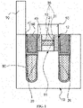
- the semiconductor structure comprises: a substrate 10; word lines 20 located in the substrate 10, a bit line contact hole 11 being provided between each two adjacent word lines 20; bit line contact plugs 30 located in the bit line contact holes 11; and first isolation layers 40 located on side walls of the bit line contact holes 11 and cover side walls of the bit line contact plugs 30.
- the first isolation layer 40 covers the side wall of the bit line contact hole 11, that is, the first isolation layer 40 is arranged between the side walls of the bit line contact plug 30 and the bit line contact hole 11, so that a coupling effect between the bit line contact plug 30 and the word lines 20 can be reduced, and thus the performance of the semiconductor structure can be improved.
- the word line 20 is an embedded word line.
- a bit line contact hole 11 is provided between two word lines 20.
- a bottom wall of the bit line contact hole 11 is higher than a top surface of the word line 20. That is, a bottom surface of the bit line contact plug 30 is higher than the top surface of the word line 20.
- the substrate 10 may comprise a semiconductor substrate.
- the semiconductor substrate may be formed of a silicon-containing material.
- the semiconductor substrate may be formed of any suitable material, including, e.g., at least one of silicon, monocrystalline silicon, polycrystalline silicon, amorphous silicon, silicon germanium, monocrystalline silicon germanium, polycrystalline silicon germanium, and carbon-doped silicon.
- the word line 20 comprises a metal material, which may comprise at least one of tungsten nitride (WN), molybdenum nitride (MoN), titanium nitride (TIN), tantalum nitride (TaN), titanium silicon nitride (TiSiN), tantalum silicon nitride (TaSiN), or tungsten (W).
- WN tungsten nitride
- MoN molybdenum nitride
- TiN titanium nitride
- TaN titanium silicon nitride
- TaSiN tantalum silicon nitride
- W tungsten
- the semiconductor structure further comprises a bit line 50.
- the bit line 50 is located on the bit line contact plug 30. That is, the bit line 50 is connected to the bit line contact plug 30.
- the bit line 50 comprises a metal material, which may comprise at least one of tungsten nitride (WN), molybdenum nitride (MoN), titanium nitride (TIN), tantalum nitride (TaN), titanium silicon nitride (TiSiN), tantalum silicon nitride (TaSiN), or tungsten (W).
- WN tungsten nitride
- MoN molybdenum nitride
- TiN titanium nitride
- TaN titanium silicon nitride
- TaSiN tantalum silicon nitride
- W tungsten
- bit line 50 covers an upper surface of the bit line contact plug 30.
- the first isolation layer 40 comprises a silicon oxide layer and a silicon nitride layer.
- the silicon oxide layer is in contact with the side wall of the bit line contact hole 11.
- the silicon nitride layer is in contact with the bit line contact plug 30.
- the arrangement of the silicon nitride layer may prevent the metal material in the bit line contact plug 30 from diffusing into the silicon oxide layer.
- the bit line contact plug 30 comprises polycrystalline silicon 31 and a metal material 32.
- the silicon nitride layer may cover only the metal material 32, although it may also completely cover the bit line contact plug 30.
- the bit line contact plug 30 comprises two layers of polycrystalline silicon 31 and a metal material 32 located therebetween.
- the silicon nitride layer may cover only the upper layer of polycrystalline silicon 31 and the metal material 32, but not cover the lower layer of polycrystalline silicon 31. This arrangement not only isolates the metal material from the silicon oxide layer, but also increases the contact area of the lower layer of polycrystalline silicon 31 with the substrate 10, thereby further reducing the contact resistance.
- the resistance value of the bit line contact plug 30 can be reduced when the bit line contact plug 30 comprises the metal material 32, and the contact area of the lower layer of polycrystalline silicon 31 with the substrate 10 can be increased when the lower layer of polycrystalline silicon 31 does not cover the silicon nitride layer, thereby further reducing the contact resistance.
- a thickness of the silicon nitride layer may be smaller than a thickness of the silicon oxide layer.
- the silicon nitride layer may have a thickness of Inm -3 nm.
- the silicon nitride layer has a thickness of 1 nm, 1.5 nm, 2 nm, 2.5 nm, or 3 nm.
- a bottom end of the first isolation layer 40 is flush with a bottom end of the bit line contact plug 30, and/or, the first isolation layer 40 is not lower than an upper surface of the substrate 10.
- an upper surface of the first isolation layer 40 may be flush with the upper surface of the substrate 10.
- an upper surface of the first isolation layer 40 may be higher than the upper surface of the substrate 10. That is, the bit line contact plug 30 protrudes beyond the upper surface of the substrate 10.
- the bit line contact plug 30 is a multi-layer structure, which comprises polycrystalline silicon 31 and a metal material 32.
- the arrangement of the metal material 32 may reduce the resistance value of the bit line contact plug 30.
- the metal material 32 may be copper (Cu), aluminum (Al), tungsten (W), or alloys thereof, and may be selected according to practical requirements without further limitation herein.
- the bit line contact plug 30 is a three-layer structure in which the metal material 32 is sandwiched between two layers of polycrystalline silicon 31.
- the polycrystalline silicon 31 may be ion-doped, doped elements may be boron (B), phosphorus (P), or arsenic (As).
- the polycrystalline silicon may be doped with the element of phosphorus (P).
- the polycrystalline silicon may be ion-doped with other elements.
- the ion doped concentrations of the two layers of polycrystalline silicon 31 may be equal.
- the ion doped concentrations of the two layers of polycrystalline silicon 31 may be unequal.
- the ion doped concentration of the lower layer of polycrystalline silicon 31 is higher than the ion doped concentration of the upper layer of polycrystalline silicon 31.
- the ion doped concentration of the lower layer of polycrystalline silicon 31 is high, the contact resistance with an active region of the substrate 10 can be reduced, and since the ion doped concentration of the upper layer of polycrystalline silicon 31 is low, the coupling effect between the bit line contact plug 30 and the word line 20 can be further reduced.
- the upper layer of polycrystalline silicon 31 may have an ion doped concentration of 1E20-1E21, and the lower layer of polycrystalline silicon 31 may have an ion doped concentration of 5E20-5E21.
- the metal material 32 is not higher than the upper surface of the substrate 10. That is, the metal material 32 is located in the bit line contact hole 11, and the upper surface of the bit line contact plug 30 may be higher than the upper surface of the substrate 10.
- the bit line contact plug 30 comprises polycrystalline silicon 31.
- the polycrystalline silicon 31 is ion-doped to meet the conductivity requirements, and the polycrystalline silicon 31 may be doped with phosphorus (P).
- the bit line contact plug 30 consists only of ion-doped polycrystalline silicon 31.
- the semiconductor structure further comprises second isolation layers 70 and word line surface layers 60.
- the second isolation layers 70 are located on the word lines 20.
- the word line surface layers 60 are located in the second isolation layers 70.
- the second isolation layers 70 cover side walls and bottom walls of the word line surface layers 60.
- the bit line contact plug 30 is located between two adjacent second isolation layers 70.
- the word line surface layers 60 and the second isolation layers 70 are also filled in the substrate 10 to embed the word lines 20 in the substrate 10 and achieve an insulation and isolation function.
- the semiconductor structure further comprises nitride layers, located between the second isolation layers 70 and the word lines 20, thereby preventing the metal materials of the word lines 20 from diffusing into the second isolation layers 70.
- a thickness of the nitride layer is smaller than a thickness of the second isolation layer 70.
- the nitride layer may comprise silicon nitride.
- the second isolation layer 70 may comprise silicon oxide.
- the word line surface layer 60 comprises silicon nitride. That is, the second isolation layer 70 may form an ONO-layer structure of silicon oxide-silicon nitride-silicon oxide with the word line surface layer 60.
- a bottom end of the first isolation layer 40 is higher than a bottom end of the second isolation layer 70.
- the thickness of the second isolation layer 70 is greater than a thickness of a third isolation layer 80.
- the first isolation layer 40 is in contact with the second isolation layer 70.
- the semiconductor structure further comprises third isolation layers 80.
- the third isolation layers 80 are located in the substrate 10, and cover the side walls and the bottom walls of the word lines 20. Top ends of the third isolation layers 80 are in contact with bottom ends of the second isolation layers 70.
- the third isolation layer 80 comprises a silicon oxide layer and a work function layer.
- the work function layer is in contact with the word line 20 and the silicon oxide layer is in contact with the substrate 10.
- the semiconductor structure further comprises a capacitor 90.
- the capacitor 90 is located on the substrate 10.
- the capacitor 90 and the bit line 50 are located on two sides of the word line 20 respectively.
- An embodiment of the present application also provides a method for manufacturing a semiconductor structure.
- the method for manufacturing the semiconductor structure comprises the following operations.
- a substrate 10 is provided.
- word lines 20 are formed in the substrate 10, and a bit line contact hole 11 is formed between two adjacent word lines 20.
- a first isolation layer 40 is formed on a side wall of the bit line contact hole 11.
- a bit line contact plug 30 is formed in the first isolation layer 40.
- the first isolation layer 40 covers a side wall of the bit line contact plug 30.
- the first isolation layer 40 covers the side wall of the bit line contact hole 11, and the bit line contact plug 30 is formed in the first isolation layer 40, so that the first isolation layer 40 is formed between the bit line contact plug 30 and the side wall of the bit line contact hole 11.
- a coupling effect between the bit line contact plug 30 and the word line 20 can be reduced by the first isolation layer 40, and thus the performance of the semiconductor structure can be improved.
- word lines 20 is not limited herein, and the word lines may be formed according to methods in the related art.
- a trench is etched in the substrate 10, a third isolation layer 80 covers a wall of the trench, and then the third isolation layer 80 is filled with a conductive material, so as to form the word line 20.
- the third isolation layer 80 may comprise a silicon oxide layer and a work function layer. That is, the wall of the trench is covered with the silicon oxide layer, the silicon oxide layer is then covered with the work function layer, and the word line 20 is formed in the work function layer finally.
- the word line 20 may comprise at least one of tungsten nitride (WN), molybdenum nitride (MoN), titanium nitride (TIN), tantalum nitride (TaN), titanium silicon nitride (TiSiN), tantalum silicon nitride (TaSiN), or tungsten (W).
- WN tungsten nitride
- MoN molybdenum nitride
- TiN titanium nitride
- TaN tantalum nitride
- TiSiN titanium silicon nitride
- TaSiN tantalum silicon nitride
- W tungsten
- the method for manufacturing the semiconductor structure comprises the following operations.
- a bit line 50 is formed on the bit line contact plug 30, and a capacitor 90 is formed on the substrate 10.
- the bit line 50 may comprise at least one of tungsten nitride (WN), molybdenum nitride (MoN), titanium nitride (TIN), tantalum nitride (TaN), titanium silicon nitride (TiSiN), tantalum silicon nitride (TaSiN), or tungsten (W).
- WN tungsten nitride
- MoN molybdenum nitride
- TiN titanium nitride
- TaN tantalum nitride
- TiSiN titanium silicon nitride
- TaSiN tantalum silicon nitride
- W tungsten
- the step of forming the bit line contact plug 30 comprises the following operations.
- Polycrystalline silicon 31 is covered in the first isolation layer 40.
- the polycrystalline silicon 31 covers the bit line contact hole 11.
- a metal material 32 is covered on the polycrystalline silicon 31.
- Polycrystalline silicon 31 is covered on the metal material 32.
- the bit line contact plug 30 is formed of three layers of materials. First, polycrystalline silicon 31 is filled in the first isolation layer 40, i.e. a lower layer of polycrystalline silicon 31 is formed. The lower layer of polycrystalline silicon 31 is located in the bit line contact hole 11. Then, a metal material 32 is covered on the lower layer of polycrystalline silicon 31. The metal material 32 is also located in the bit line contact hole 11. At this point, the metal material 32 is not higher than the upper surface of the substrate 10. Finally, polycrystalline silicon 31 is covered above the metal material 32 to form an upper layer of polycrystalline silicon 31.
- the formed polycrystalline silicon 31 is ion-doped.
- An ion-doped polycrystalline silicon material may be directly filled into the first isolation layer 40.
- polycrystalline silicon not doped with ions may be filled first, and after the filling of the polycrystalline silicon is completed, ion implantation is performed to form the ion-doped polycrystalline silicon 31.
- the specific forming mode is not limited herein and may be selected according to practical requirements.
- the polycrystalline silicon 31 may be doped with phosphorus (P).
- the doped elements may be boron (B), arsenic (As), or other ions.
- the ion doped concentrations of the two layers of polycrystalline silicon 31 may be equal. Or, the ion doped concentrations of the two layers of polycrystalline silicon 31 may not be equal.
- the ion doped concentration of the lower layer of polycrystalline silicon 31 may be higher than the ion doped concentration of the upper layer of polycrystalline silicon 31.
- the upper layer of polycrystalline silicon 31 may have an ion doped concentration of 1E20-1E21, and the lower layer of polycrystalline silicon 31 may have an ion doped concentration of 5E20-5E21.
- the metal material 32 may be copper (Cu), aluminum (Al), tungsten (W), or alloys thereof, etc.
- the step of forming the bit line contact plug 30 comprises the following operations.
- Polycrystalline silicon 31 is filled in the first isolation layer 40. That is, the bit line contact plug 30 is formed only of polycrystalline silicon 31.
- the polycrystalline silicon 31 may be doped with phosphorus (P).
- a second isolation layer 70 is formed on the word line 20.
- a word line surface layer 60 is formed in the second isolation layer 70.
- the second isolation layer 70 covers a side wall and a bottom wall of the word line surface layer 60.
- a trench is formed in the substrate 10, and a third isolation layer 80 and a word line 20 are formed at a lower portion of the trench. Then, a second isolation layer 70 is formed on upper surfaces of the third isolation layer 80 and the word line 20. The second isolation layer 70 covers a side wall of the trench and the upper surfaces of the third isolation layer 80 and the word line 20.
- a nitride layer may be formed on the upper surface of the word line 20, and then the second isolation layer 70 may be formed on the nitride layer.
- the second isolation layer 70 is connected to the silicon oxide layer of the third isolation layer 80, and the second isolation layer 70 may comprise silicon oxide.
- the nitride layer may comprise silicon nitride.
- the nitride layer may be formed using a Remote Plasma Nitridation (RPN) process.
- RPN Remote Plasma Nitridation
- a word line surface layer 60 is formed in the second isolation layer 70.
- the word line surface layer 60 comprises silicon nitride.
- the third isolation layer 80, the second isolation layer 70, and the word line surface layer 60 may be formed using a Physical Vapor Deposition (PVD) process, a Chemical Vapor Deposition (CVD) process, or an Atomic Layer Deposition (ALD) process. Etching or Chemical Mechanical Polishing (CMP) may be used for corresponding processing after formation to obtain the structures of FIGS. 3 and 4 , and may be selected according to practical requirements without limitation herein.
- PVD Physical Vapor Deposition
- CVD Chemical Vapor Deposition
- ALD Atomic Layer Deposition
- CMP Chemical Mechanical Polishing
- the step of forming the first isolation layer 40 comprises the following operations.
- An opening 12 is formed on the substrate 10, and the second isolation layer 70 is exposed.
- the opening 12 serves as the bit line contact hole 11.
- the first isolation layer 40 is formed on a side wall of the opening 12.
- the opening 12 is formed between two second isolation layers 70, and the first isolation layer 40 is formed in the opening 12.
- the first isolation layer 40 may be formed using a Physical Vapor Deposition (PVD) process, a Chemical Vapor Deposition (CVD) process, or an Atomic Layer Deposition (ALD) process.
- PVD Physical Vapor Deposition
- CVD Chemical Vapor Deposition
- ALD Atomic Layer Deposition
- an isolation layer is deposited in the bit line contact hole 11 by using an ALD process, the isolation layer at the bottom of the bit line contact hole 11 and the isolation layer on the upper surface of the substrate are removed by etching, and the isolation layer on the side wall of the bit line contact hole 11 is retained, so that the first isolation layer 40 is formed, thereby forming the structure shown in FIG. 5 .
- FIG. 5 As shown in conjunction with FIG.
- bit line contact plug 30 A bit line 50 is formed on the bit line contact plug 30 and a capacitor 90 is formed on the substrate 10, to form the semiconductor structure shown in FIG. 1 .
- the first isolation layer 40 comprises a silicon oxide layer and a silicon nitride layer. That is, the silicon oxide layer is first formed on the side wall of the bit line contact hole 11 (i.e. the side wall of the opening 12). Then, the silicon nitride layer is formed on a side wall of the silicon oxide layer. Finally, the bit line contact plug 30 is formed in the silicon nitride layer.
- the silicon nitride layer may have a thickness of 1 nm-3 nm.
Landscapes
- Engineering & Computer Science (AREA)
- Manufacturing & Machinery (AREA)
- Semiconductor Memories (AREA)
- Internal Circuitry In Semiconductor Integrated Circuit Devices (AREA)
- Metal-Oxide And Bipolar Metal-Oxide Semiconductor Integrated Circuits (AREA)
Abstract
Description
- The present application claims priority to
Chinese patent application No. 202010878114.1, filed on August 27, 2020 - The present application relates to the technical field of semiconductors, and in particular to a semiconductor structure and a method for manufacturing a semiconductor structure.
- With the increasing integration of semiconductors and the gradually reduction of a circuit dimension, a coupling phenomenon between bit line contact plugs and word lines is caused, thereby affecting device performance.
- The present application provides a semiconductor structure and a method for manufacturing a semiconductor structure, to improve the performance of the semiconductor structure.
- According to a first aspect of the present application, a semiconductor structure is provided. The semiconductor structure comprises:
- a substrate;
- word lines, located in the substrate, each of bit line contact holes being provided between two adjacent word lines;
- bit line contact plugs, located in the bit line contact holes; and
- first isolation layers, located on side walls of the bit line contact holes and covering side walls of the bit line contact plugs.
- In an embodiment of the present application, the first isolation layer may comprise a silicon oxide layer and a silicon nitride layer. The silicon oxide layer may be in contact with the side wall of the bit line contact hole. The silicon nitride layer may be in contact with the bit line contact plug.
- In an embodiment of the present application, a bottom end of the first isolation layer may be flush with a bottom end of the bit line contact plug, and/or, the first isolation layer may be not lower than an upper surface of the substrate.
- In an embodiment of the present application, the bit line contact plug may be a multi-layer structure. The multi-layer structure may comprise polycrystalline silicon and a metal material.
- In an embodiment of the present application, the bit line contact plug may be a three-layer structure in which the metal material is sandwiched between two layers of polycrystalline silicon.
- In an embodiment of the present application, the metal material may be not higher than the upper surface of the substrate.
- In an embodiment of the present application, the bit line contact plug may comprise polycrystalline silicon.
- In an embodiment of the present application, the semiconductor structure may further comprise:
- second isolation layers, located on the word lines; and
- word line surface layers, located in the second isolation layers, the second isolation layers covering side walls and bottom walls of the word line surface layers.
- The bit line contact plug is located between two adjacent second isolation layers.
- In an embodiment of the present application, the semiconductor structure may further comprise: nitride layers, located between the second isolation layers and the word lines.
- In an embodiment of the present application, a bottom end of the first isolation layer may be higher than a bottom end of the second isolation layer.
- In an embodiment of the present application, the semiconductor structure may further comprise: a capacitor, located on the substrate.
- According to a second aspect of the present application, a method for manufacturing a semiconductor structure is provided. The method for manufacturing the semiconductor structure comprises:
- providing a substrate;
- forming word lines in the substrate, and forming a bit line contact hole between two adjacent word lines;
- forming a first isolation layer on a side wall of the bit line contact hole; and
- forming a bit line contact plug in the first isolation layer, the first isolation layer covering a side wall of the bit line contact plug.
- In an embodiment of the present application, forming the bit line contact plug may comprise:
- covering polycrystalline silicon in the first isolation layer, the polycrystalline silicon covering the bit line contact hole;
- covering a metal material on the polycrystalline silicon; and
- covering polycrystalline silicon on the metal material.
- In an embodiment of the present application, before forming the first isolation layer, the method for manufacturing the semiconductor structure may further comprise:
- forming second isolation layers on the word lines; and
- forming word line surface layers in the second isolation layers, the second isolation layers covering side walls and bottom walls of the word line surface layers.
- In an embodiment of the present application, forming the first isolation layer may comprise:
- forming an opening on the substrate, and exposing the second isolation layers, the opening serving as the bit line contact hole; and
- forming the first isolation layer on a side wall of the opening.
- According to the semiconductor structure of the present application, the first isolation layer covers the side wall of the bit line contact hole. That is, the first isolation layer is arranged between the bit line contact plug and the side wall of the bit line contact hole, so that a coupling effect between the bit line contact plug and the word line can be reduced, and thus the performance of the semiconductor structure can be improved.
- Various objects, features, and advantages of the present application will become more apparent from the following detailed description of preferred implementations of the present application when considered in conjunction with the accompanying drawings. The drawings are merely exemplary illustrations of the present application and are not necessarily drawn to scale. In the drawings, like reference numerals refer to the same or similar components throughout, where:
-
FIG. 1 is a schematic structure diagram of a semiconductor structure according to an exemplary implementation. -
FIG. 2 is a schematic flowchart of a method for manufacturing a semiconductor structure according to an exemplary implementation. -
FIG. 3 is a schematic structure diagram of a second isolation layer obtained using a method for manufacturing a semiconductor structure according to an exemplary implementation. -
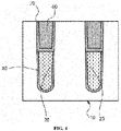
FIG. 4 is a schematic structure diagram of a word line surface layer obtained using a method for manufacturing a semiconductor structure according to an exemplary implementation. -
FIG. 5 is a schematic structure diagram of a first isolation layer obtained using a method for manufacturing a semiconductor structure according to an exemplary implementation. -
FIG. 6 is a schematic structure diagram of a bit line contact plug obtained using a method for manufacturing a semiconductor structure according to an exemplary implementation. - Reference Numerals:
10: substrate; 11: bit line contact hole; 12: opening; 20, word line; 30: bit line contact plug; 31: polycrystalline silicon; 32: metal material; 40: first isolation layer; 50: bit line; 60: word line surface layer; 70: second isolation layer; 80: third isolation layer; 90: capacitor. - Exemplary embodiments that embody the features and advantages of the present application will be described in detail in the following description. It will be appreciated that the present application may have various changes in different embodiments without departing from the scope of the present application, and that the description and drawings are illustrative in nature and are not intended to limit the present application.
- In the following description of various exemplary implementations of the present application, reference is made to the accompanying drawings, which form a part of the present application, and in which various exemplary structures, systems, and steps capable of implementing various aspects of the present application are shown by way of examples. It will be appreciated that other specific solutions of components, structures, exemplary devices, systems, and steps may be utilized and structural and functional modifications may be made without departing from the scope of the present application. Moreover, although the terms "on", "between", "in", etc. may be used in this specification to describe different exemplary features and elements of the present application, these terms are used herein for convenience only, e.g., in accordance with the orientation of the examples in the figures. Nothing in this specification should be construed as requiring a particular three-dimensional orientation of the structure to fall within the scope of the present application.
- An embodiment of the present application provides a semiconductor structure. Referring to
FIG. 1 , the semiconductor structure comprises: asubstrate 10; word lines 20 located in thesubstrate 10, a bitline contact hole 11 being provided between each two adjacent word lines 20; bit line contact plugs 30 located in the bit line contact holes 11; and first isolation layers 40 located on side walls of the bit line contact holes 11 and cover side walls of the bit line contact plugs 30. - According to the semiconductor structure of an embodiment of the present application, the
first isolation layer 40 covers the side wall of the bitline contact hole 11, that is, thefirst isolation layer 40 is arranged between the side walls of the bitline contact plug 30 and the bitline contact hole 11, so that a coupling effect between the bitline contact plug 30 and the word lines 20 can be reduced, and thus the performance of the semiconductor structure can be improved. - It is noted that the
word line 20 is an embedded word line. A bitline contact hole 11 is provided between two word lines 20. A bottom wall of the bitline contact hole 11 is higher than a top surface of theword line 20. That is, a bottom surface of the bitline contact plug 30 is higher than the top surface of theword line 20. - In an embodiment, the
substrate 10 may comprise a semiconductor substrate. The semiconductor substrate may be formed of a silicon-containing material. The semiconductor substrate may be formed of any suitable material, including, e.g., at least one of silicon, monocrystalline silicon, polycrystalline silicon, amorphous silicon, silicon germanium, monocrystalline silicon germanium, polycrystalline silicon germanium, and carbon-doped silicon. - In an embodiment, the
word line 20 comprises a metal material, which may comprise at least one of tungsten nitride (WN), molybdenum nitride (MoN), titanium nitride (TIN), tantalum nitride (TaN), titanium silicon nitride (TiSiN), tantalum silicon nitride (TaSiN), or tungsten (W). The specific structure of theword line 20 is not limited herein, and structures known in the related art may be employed. - In an embodiment, as shown in
FIG. 1 , the semiconductor structure further comprises abit line 50. Thebit line 50 is located on the bitline contact plug 30. That is, thebit line 50 is connected to the bitline contact plug 30. - In an embodiment, the
bit line 50 comprises a metal material, which may comprise at least one of tungsten nitride (WN), molybdenum nitride (MoN), titanium nitride (TIN), tantalum nitride (TaN), titanium silicon nitride (TiSiN), tantalum silicon nitride (TaSiN), or tungsten (W). The specific structure of thebit line 50 is not limited herein, and structures known in the related art may be employed. - In an embodiment, the
bit line 50 covers an upper surface of the bitline contact plug 30. - In an embodiment, the
first isolation layer 40 comprises a silicon oxide layer and a silicon nitride layer. The silicon oxide layer is in contact with the side wall of the bitline contact hole 11. The silicon nitride layer is in contact with the bitline contact plug 30. In view of the arrangement of the metal material in the bitline contact plug 30, the arrangement of the silicon nitride layer may prevent the metal material in the bit line contact plug 30 from diffusing into the silicon oxide layer. - Specifically, for example, the bit
line contact plug 30 comprisespolycrystalline silicon 31 and ametal material 32. At this point, the silicon nitride layer may cover only themetal material 32, although it may also completely cover the bitline contact plug 30. As shown inFIG. 1 , the bitline contact plug 30 comprises two layers ofpolycrystalline silicon 31 and ametal material 32 located therebetween. At this point, the silicon nitride layer may cover only the upper layer ofpolycrystalline silicon 31 and themetal material 32, but not cover the lower layer ofpolycrystalline silicon 31. This arrangement not only isolates the metal material from the silicon oxide layer, but also increases the contact area of the lower layer ofpolycrystalline silicon 31 with thesubstrate 10, thereby further reducing the contact resistance. - It is noted that the resistance value of the bit
line contact plug 30 can be reduced when the bitline contact plug 30 comprises themetal material 32, and the contact area of the lower layer ofpolycrystalline silicon 31 with thesubstrate 10 can be increased when the lower layer ofpolycrystalline silicon 31 does not cover the silicon nitride layer, thereby further reducing the contact resistance. - In an embodiment, a thickness of the silicon nitride layer may be smaller than a thickness of the silicon oxide layer. For example, the silicon nitride layer may have a thickness of Inm -3 nm. Specifically, the silicon nitride layer has a thickness of 1 nm, 1.5 nm, 2 nm, 2.5 nm, or 3 nm.
- In an embodiment, a bottom end of the
first isolation layer 40 is flush with a bottom end of the bitline contact plug 30, and/or, thefirst isolation layer 40 is not lower than an upper surface of thesubstrate 10. - It is noted that an upper surface of the
first isolation layer 40 may be flush with the upper surface of thesubstrate 10. Alternatively, an upper surface of thefirst isolation layer 40 may be higher than the upper surface of thesubstrate 10. That is, the bitline contact plug 30 protrudes beyond the upper surface of thesubstrate 10. - In an embodiment, the bit
line contact plug 30 is a multi-layer structure, which comprisespolycrystalline silicon 31 and ametal material 32. The arrangement of themetal material 32 may reduce the resistance value of the bitline contact plug 30. Themetal material 32 may be copper (Cu), aluminum (Al), tungsten (W), or alloys thereof, and may be selected according to practical requirements without further limitation herein. - In an embodiment, as shown in
FIG. 1 , the bitline contact plug 30 is a three-layer structure in which themetal material 32 is sandwiched between two layers ofpolycrystalline silicon 31. - It is noted that the
polycrystalline silicon 31 may be ion-doped, doped elements may be boron (B), phosphorus (P), or arsenic (As). In the present embodiment, the polycrystalline silicon may be doped with the element of phosphorus (P). In other embodiments, the polycrystalline silicon may be ion-doped with other elements. In an embodiment, the ion doped concentrations of the two layers ofpolycrystalline silicon 31 may be equal. Alternatively, the ion doped concentrations of the two layers ofpolycrystalline silicon 31 may be unequal. For example, the ion doped concentration of the lower layer ofpolycrystalline silicon 31 is higher than the ion doped concentration of the upper layer ofpolycrystalline silicon 31. At this point, since the ion doped concentration of the lower layer ofpolycrystalline silicon 31 is high, the contact resistance with an active region of thesubstrate 10 can be reduced, and since the ion doped concentration of the upper layer ofpolycrystalline silicon 31 is low, the coupling effect between the bitline contact plug 30 and theword line 20 can be further reduced. - Specifically, the upper layer of
polycrystalline silicon 31 may have an ion doped concentration of 1E20-1E21, and the lower layer ofpolycrystalline silicon 31 may have an ion doped concentration of 5E20-5E21. - In an embodiment, the
metal material 32 is not higher than the upper surface of thesubstrate 10. That is, themetal material 32 is located in the bitline contact hole 11, and the upper surface of the bitline contact plug 30 may be higher than the upper surface of thesubstrate 10. - In an embodiment, the bit
line contact plug 30 comprisespolycrystalline silicon 31. Thepolycrystalline silicon 31 is ion-doped to meet the conductivity requirements, and thepolycrystalline silicon 31 may be doped with phosphorus (P). Specifically, the bitline contact plug 30 consists only of ion-dopedpolycrystalline silicon 31. - In an embodiment, as shown in
FIG. 1 , the semiconductor structure further comprises second isolation layers 70 and word line surface layers 60. The second isolation layers 70 are located on the word lines 20. The word line surface layers 60 are located in the second isolation layers 70. The second isolation layers 70 cover side walls and bottom walls of the word line surface layers 60. The bitline contact plug 30 is located between two adjacent second isolation layers 70. The word line surface layers 60 and the second isolation layers 70 are also filled in thesubstrate 10 to embed the word lines 20 in thesubstrate 10 and achieve an insulation and isolation function. - In an embodiment, the semiconductor structure further comprises nitride layers, located between the second isolation layers 70 and the word lines 20, thereby preventing the metal materials of the word lines 20 from diffusing into the second isolation layers 70.
- It is noted that a thickness of the nitride layer is smaller than a thickness of the
second isolation layer 70. The nitride layer may comprise silicon nitride. Thesecond isolation layer 70 may comprise silicon oxide. - In an embodiment, the word
line surface layer 60 comprises silicon nitride. That is, thesecond isolation layer 70 may form an ONO-layer structure of silicon oxide-silicon nitride-silicon oxide with the wordline surface layer 60. - In an embodiment, a bottom end of the
first isolation layer 40 is higher than a bottom end of thesecond isolation layer 70. - In an embodiment, the thickness of the
second isolation layer 70 is greater than a thickness of athird isolation layer 80. - In an embodiment, the
first isolation layer 40 is in contact with thesecond isolation layer 70. - In an embodiment, as shown in
FIG. 1 , the semiconductor structure further comprises third isolation layers 80. The third isolation layers 80 are located in thesubstrate 10, and cover the side walls and the bottom walls of the word lines 20. Top ends of the third isolation layers 80 are in contact with bottom ends of the second isolation layers 70. - It is noted that the
third isolation layer 80 comprises a silicon oxide layer and a work function layer. The work function layer is in contact with theword line 20 and the silicon oxide layer is in contact with thesubstrate 10. - In an embodiment, as shown in
FIG. 1 , the semiconductor structure further comprises acapacitor 90. Thecapacitor 90 is located on thesubstrate 10. Thecapacitor 90 and thebit line 50 are located on two sides of theword line 20 respectively. - An embodiment of the present application also provides a method for manufacturing a semiconductor structure. Referring to
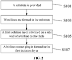
FIG. 2 , the method for manufacturing the semiconductor structure comprises the following operations. - At S101, a
substrate 10 is provided. - At S103, word lines 20 are formed in the
substrate 10, and a bitline contact hole 11 is formed between two adjacent word lines 20. - At S105, a
first isolation layer 40 is formed on a side wall of the bitline contact hole 11. - At S107, a bit
line contact plug 30 is formed in thefirst isolation layer 40. Thefirst isolation layer 40 covers a side wall of the bitline contact plug 30. - According to the method for manufacturing the semiconductor structure of an embodiment of the present application, the
first isolation layer 40 covers the side wall of the bitline contact hole 11, and the bitline contact plug 30 is formed in thefirst isolation layer 40, so that thefirst isolation layer 40 is formed between the bitline contact plug 30 and the side wall of the bitline contact hole 11. A coupling effect between the bitline contact plug 30 and theword line 20 can be reduced by thefirst isolation layer 40, and thus the performance of the semiconductor structure can be improved. - It is noted that the particular forming method for the word lines 20 is not limited herein, and the word lines may be formed according to methods in the related art.
- For example, a trench is etched in the
substrate 10, athird isolation layer 80 covers a wall of the trench, and then thethird isolation layer 80 is filled with a conductive material, so as to form theword line 20. Thethird isolation layer 80 may comprise a silicon oxide layer and a work function layer. That is, the wall of the trench is covered with the silicon oxide layer, the silicon oxide layer is then covered with the work function layer, and theword line 20 is formed in the work function layer finally. - Specifically, the
word line 20 may comprise at least one of tungsten nitride (WN), molybdenum nitride (MoN), titanium nitride (TIN), tantalum nitride (TaN), titanium silicon nitride (TiSiN), tantalum silicon nitride (TaSiN), or tungsten (W). - In an embodiment, the method for manufacturing the semiconductor structure comprises the following operations. A
bit line 50 is formed on the bitline contact plug 30, and acapacitor 90 is formed on thesubstrate 10. - In an embodiment, the
bit line 50 may comprise at least one of tungsten nitride (WN), molybdenum nitride (MoN), titanium nitride (TIN), tantalum nitride (TaN), titanium silicon nitride (TiSiN), tantalum silicon nitride (TaSiN), or tungsten (W). - In an embodiment, the step of forming the bit
line contact plug 30 comprises the following operations.Polycrystalline silicon 31 is covered in thefirst isolation layer 40. Thepolycrystalline silicon 31 covers the bitline contact hole 11. Ametal material 32 is covered on thepolycrystalline silicon 31.Polycrystalline silicon 31 is covered on themetal material 32. - The bit
line contact plug 30 is formed of three layers of materials. First,polycrystalline silicon 31 is filled in thefirst isolation layer 40, i.e. a lower layer ofpolycrystalline silicon 31 is formed. The lower layer ofpolycrystalline silicon 31 is located in the bitline contact hole 11. Then, ametal material 32 is covered on the lower layer ofpolycrystalline silicon 31. Themetal material 32 is also located in the bitline contact hole 11. At this point, themetal material 32 is not higher than the upper surface of thesubstrate 10. Finally,polycrystalline silicon 31 is covered above themetal material 32 to form an upper layer ofpolycrystalline silicon 31. - It is noted that the formed
polycrystalline silicon 31 is ion-doped. An ion-doped polycrystalline silicon material may be directly filled into thefirst isolation layer 40. Alternatively, polycrystalline silicon not doped with ions may be filled first, and after the filling of the polycrystalline silicon is completed, ion implantation is performed to form the ion-dopedpolycrystalline silicon 31. The specific forming mode is not limited herein and may be selected according to practical requirements. - In an embodiment, the
polycrystalline silicon 31 may be doped with phosphorus (P). In other embodiments, the doped elements may be boron (B), arsenic (As), or other ions. The ion doped concentrations of the two layers ofpolycrystalline silicon 31 may be equal. Or, the ion doped concentrations of the two layers ofpolycrystalline silicon 31 may not be equal. For example, the ion doped concentration of the lower layer ofpolycrystalline silicon 31 may be higher than the ion doped concentration of the upper layer ofpolycrystalline silicon 31. The upper layer ofpolycrystalline silicon 31 may have an ion doped concentration of 1E20-1E21, and the lower layer ofpolycrystalline silicon 31 may have an ion doped concentration of 5E20-5E21. - In an embodiment, the
metal material 32 may be copper (Cu), aluminum (Al), tungsten (W), or alloys thereof, etc. - In an embodiment, the step of forming the bit
line contact plug 30 comprises the following operations.Polycrystalline silicon 31 is filled in thefirst isolation layer 40. That is, the bitline contact plug 30 is formed only ofpolycrystalline silicon 31. Thepolycrystalline silicon 31 may be doped with phosphorus (P). - In an embodiment, before forming the
first isolation layer 40, the following operations are further included. Asecond isolation layer 70 is formed on theword line 20. A wordline surface layer 60 is formed in thesecond isolation layer 70. Thesecond isolation layer 70 covers a side wall and a bottom wall of the wordline surface layer 60. - As shown in conjunction with
FIG. 3 , a trench is formed in thesubstrate 10, and athird isolation layer 80 and aword line 20 are formed at a lower portion of the trench. Then, asecond isolation layer 70 is formed on upper surfaces of thethird isolation layer 80 and theword line 20. Thesecond isolation layer 70 covers a side wall of the trench and the upper surfaces of thethird isolation layer 80 and theword line 20. - It is noted that before forming the
second isolation layer 70, a nitride layer may be formed on the upper surface of theword line 20, and then thesecond isolation layer 70 may be formed on the nitride layer. Thesecond isolation layer 70 is connected to the silicon oxide layer of thethird isolation layer 80, and thesecond isolation layer 70 may comprise silicon oxide. The nitride layer may comprise silicon nitride. The nitride layer may be formed using a Remote Plasma Nitridation (RPN) process. - As shown in conjunction with
FIG. 4 , a wordline surface layer 60 is formed in thesecond isolation layer 70. The wordline surface layer 60 comprises silicon nitride. - It is noted that the
third isolation layer 80, thesecond isolation layer 70, and the wordline surface layer 60 may be formed using a Physical Vapor Deposition (PVD) process, a Chemical Vapor Deposition (CVD) process, or an Atomic Layer Deposition (ALD) process. Etching or Chemical Mechanical Polishing (CMP) may be used for corresponding processing after formation to obtain the structures ofFIGS. 3 and4 , and may be selected according to practical requirements without limitation herein. - In an embodiment, the step of forming the
first isolation layer 40 comprises the following operations. Anopening 12 is formed on thesubstrate 10, and thesecond isolation layer 70 is exposed. Theopening 12 serves as the bitline contact hole 11. Thefirst isolation layer 40 is formed on a side wall of theopening 12. - Referring to
FIG. 5 , on the basis ofFIG. 4 , theopening 12 is formed between two second isolation layers 70, and thefirst isolation layer 40 is formed in theopening 12. - Specifically, the
first isolation layer 40 may be formed using a Physical Vapor Deposition (PVD) process, a Chemical Vapor Deposition (CVD) process, or an Atomic Layer Deposition (ALD) process. In the present embodiment, an isolation layer is deposited in the bitline contact hole 11 by using an ALD process, the isolation layer at the bottom of the bitline contact hole 11 and the isolation layer on the upper surface of the substrate are removed by etching, and the isolation layer on the side wall of the bitline contact hole 11 is retained, so that thefirst isolation layer 40 is formed, thereby forming the structure shown inFIG. 5 . As shown in conjunction withFIG. 6 ,polycrystalline silicon 31, ametal material 32, andpolycrystalline silicon 31 are sequentially filled in thefirst isolation layer 40 to form a bitline contact plug 30. Abit line 50 is formed on the bitline contact plug 30 and acapacitor 90 is formed on thesubstrate 10, to form the semiconductor structure shown inFIG. 1 . - It is noted that the
first isolation layer 40 comprises a silicon oxide layer and a silicon nitride layer. That is, the silicon oxide layer is first formed on the side wall of the bit line contact hole 11 (i.e. the side wall of the opening 12). Then, the silicon nitride layer is formed on a side wall of the silicon oxide layer. Finally, the bitline contact plug 30 is formed in the silicon nitride layer. The silicon nitride layer may have a thickness of 1 nm-3 nm. - After considering the specification and implementing the present application disclosed here, it is easy for those of ordinary skill in the art to conceive other implementation solutions of the present application. The present application is intended to cover any variations, uses, or adaptations of the present application following the general principles thereof and including such departures from the present application as come within known or customary practice in the art. It is intended that the specification and example implementations be considered as exemplary only, with a true scope and spirit of the present application being indicated by the claims.
- It will be understood that the present application is not limited to the exact construction that has been described above and illustrated in the accompanying drawings, and that various modifications and changes may be made without departing from the scope thereof. It is intended that the scope of the present application only be limited by the appended claims.
Claims (15)
- A semiconductor structure, characterized in that the semiconductor structure comprises:a substrate;word lines, located in the substrate, wherein each of bit line contact holes is provided between two adjacent word lines;bit line contact plugs, located in bit line contact holes; andfirst isolation layers, located on side walls of the bit line contact holes and covering side walls of the bit line contact plugs.
- The semiconductor structure of claim 1, characterized in that the first isolation layer comprises a silicon oxide layer and a silicon nitride layer, the silicon oxide layer is in contact with the side wall of the bit line contact hole, and the silicon nitride layer is in contact with the bit line contact plug.
- The semiconductor structure of claim 1, characterized in that a bottom end of the first isolation layer is flush with a bottom end of the bit line contact plug, and/or, the first isolation layer is not lower than an upper surface of the substrate.
- The semiconductor structure of any one of claims 1 to 3, characterized in that the bit line contact plug is a multi-layer structure, the multi-layer structure comprising polycrystalline silicon and a metal material.
- The semiconductor structure of claim 4, characterized in that the bit line contact plug is a three-layer structure in which the metal material is sandwiched between two layers of polycrystalline silicon.
- The semiconductor structure of claim 4, characterized in that the metal material is not higher than an upper surface of the substrate.
- The semiconductor structure of claim 1, characterized in that the bit line contact plug comprises polycrystalline silicon.
- The semiconductor structure of claim 1, characterized in that the semiconductor structure further comprises:second isolation layers, located on the word lines; andword line surface layers, located in the second isolation layers, the second isolation layers covering side walls and bottom walls of the word line surface layers,wherein the bit line contact plug is located between two adjacent second isolation layers.
- The semiconductor structure of claim 8, characterized in that the semiconductor structure further comprises:
nitride layers, located between the second isolation layers and the word lines. - The semiconductor structure of claim 8, characterized in that a bottom end of the first isolation layer is higher than a bottom end of the second isolation layer.
- The semiconductor structure of claim 1, characterized in that the semiconductor structure further comprises:
a capacitor, located on the substrate. - A method for manufacturing a semiconductor structure, characterized in that the method comprises:providing a substrate;forming word lines in the substrate, and forming a bit line contact hole between two adjacent word lines;forming a first isolation layer on a side wall of the bit line contact hole; andforming a bit line contact plug in the first isolation layer, the first isolation layer covering a side wall of the bit line contact plug.
- The method for manufacturing the semiconductor structure of claim 12, characterized in that forming the bit line contact plug comprises:covering polycrystalline silicon in the first isolation layer, the polycrystalline silicon covering the bit line contact hole;covering a metal material on the polycrystalline silicon; andcovering polycrystalline silicon on the metal material.
- The method for manufacturing the semiconductor structure of claim 12, characterized in that the method, before forming the first isolation layer, further comprises:forming second isolation layers on the word lines; andforming word line surface layers in the second isolation layers, the second isolation layers covering side walls and bottom walls of the word line surface layers.
- The method for manufacturing the semiconductor structure of claim 14, characterized in that forming the first isolation layer comprises:forming an opening in the substrate, and exposing the second isolation layers, the opening serving as the bit line contact hole; andforming the first isolation layer on a side wall of the opening.
Applications Claiming Priority (2)
| Application Number | Priority Date | Filing Date | Title |
|---|---|---|---|
| CN202010878114.1A CN114121880B (en) | 2020-08-27 | 2020-08-27 | Semiconductor structure and manufacturing method thereof |
| PCT/CN2021/101618 WO2022041981A1 (en) | 2020-08-27 | 2021-06-22 | Semiconductor structure and method for manufacturing semiconductor structure |
Publications (2)
| Publication Number | Publication Date |
|---|---|
| EP4109533A1 true EP4109533A1 (en) | 2022-12-28 |
| EP4109533A4 EP4109533A4 (en) | 2023-09-13 |
Family
ID=80354545
Family Applications (1)
| Application Number | Title | Priority Date | Filing Date |
|---|---|---|---|
| EP21859823.3A Pending EP4109533A4 (en) | 2020-08-27 | 2021-06-22 | SEMICONDUCTOR STRUCTURE AND METHOD FOR MANUFACTURING SEMICONDUCTOR STRUCTURE |
Country Status (6)
| Country | Link |
|---|---|
| US (1) | US11871561B2 (en) |
| EP (1) | EP4109533A4 (en) |
| JP (1) | JP7462064B2 (en) |
| KR (1) | KR102751826B1 (en) |
| CN (1) | CN114121880B (en) |
| WO (1) | WO2022041981A1 (en) |
Families Citing this family (1)
| Publication number | Priority date | Publication date | Assignee | Title |
|---|---|---|---|---|
| CN115988877B (en) * | 2023-03-16 | 2023-09-08 | 长鑫存储技术有限公司 | Semiconductor structure and manufacturing method thereof |
Family Cites Families (24)
| Publication number | Priority date | Publication date | Assignee | Title |
|---|---|---|---|---|
| US5589413A (en) * | 1995-11-27 | 1996-12-31 | Taiwan Semiconductor Manufacturing Company | Method of manufacturing self-aligned bit-line during EPROM fabrication |
| US5798296A (en) * | 1996-05-17 | 1998-08-25 | Micron Technology, Inc. | Method of fabricating a gate having a barrier of titanium silicide |
| KR100629270B1 (en) * | 2005-02-23 | 2006-09-29 | 삼성전자주식회사 | NAND flash memory device and manufacturing method thereof |
| US7595262B2 (en) | 2006-10-27 | 2009-09-29 | Qimonda Ag | Manufacturing method for an integrated semiconductor structure |
| KR101095817B1 (en) | 2009-02-10 | 2011-12-21 | 주식회사 하이닉스반도체 | Semiconductor element and manufacturing method thereof |
| KR101883656B1 (en) * | 2012-03-30 | 2018-07-31 | 삼성전자주식회사 | Semiconductor devices including contacts which have enlarged contact areas with actives and methods for fabricating the same |
| KR101926027B1 (en) * | 2012-08-31 | 2018-12-06 | 에스케이하이닉스 주식회사 | Semiconductor device having asymmetry bit line contact and method for manufacturing the same |
| KR101924020B1 (en) * | 2012-10-18 | 2018-12-03 | 삼성전자주식회사 | Semiconductor device and method of fabricating the same |
| KR101934366B1 (en) * | 2012-10-25 | 2019-01-02 | 삼성전자주식회사 | Semiconductor devices having recessed active regions and methods for fabricating the same |
| JP2015053477A (en) * | 2013-08-05 | 2015-03-19 | 株式会社半導体エネルギー研究所 | Semiconductor device and manufacturing method of semiconductor device |
| JP2015053447A (en) * | 2013-09-09 | 2015-03-19 | マイクロン テクノロジー, インク. | Semiconductor device, manufacturing method thereof, and data processing system |
| JP2015135885A (en) | 2014-01-17 | 2015-07-27 | マイクロン テクノロジー, インク. | Semiconductor device, and method of manufacturing the same |
| KR102164542B1 (en) * | 2014-05-21 | 2020-10-12 | 삼성전자 주식회사 | Semiconductor Devices Having Buried Gate Structures and Methods of the Same |
| JP2016009788A (en) | 2014-06-25 | 2016-01-18 | マイクロン テクノロジー, インク. | Semiconductor device |
| US9881924B2 (en) * | 2016-05-11 | 2018-01-30 | Micron Technology, Inc. | Semiconductor memory device having coplanar digit line contacts and storage node contacts in memory array and method for fabricating the same |
| KR102450577B1 (en) | 2016-08-12 | 2022-10-11 | 삼성전자주식회사 | Semiconductor devices |
| CN109148376B (en) * | 2017-06-28 | 2020-07-31 | 长鑫存储技术有限公司 | Memory and forming method thereof, and semiconductor device |
| KR102444707B1 (en) * | 2018-03-26 | 2022-09-19 | 에스케이하이닉스 주식회사 | Semiconductor device having ultra-low permittivity spacer and manufacturing method thereof |
| CN108899309A (en) | 2018-06-27 | 2018-11-27 | 长鑫存储技术有限公司 | Embedded type word line structure and preparation method thereof |
| CN110890368B (en) * | 2018-09-07 | 2024-09-20 | 长鑫存储技术有限公司 | Semiconductor device manufacturing method and semiconductor device |
| CN110890365B (en) * | 2018-09-07 | 2024-08-27 | 长鑫存储技术有限公司 | A semiconductor memory and a method for manufacturing the same |
| CN208706648U (en) * | 2018-09-07 | 2019-04-05 | 长鑫存储技术有限公司 | a semiconductor memory |
| CN108987282B (en) * | 2018-09-11 | 2023-07-21 | 长鑫存储技术有限公司 | A kind of semiconductor device and its manufacturing method |
| KR102707833B1 (en) * | 2018-12-24 | 2024-09-24 | 삼성전자주식회사 | Semiconductor Memory Device |
-
2020
- 2020-08-27 CN CN202010878114.1A patent/CN114121880B/en active Active
-
2021
- 2021-06-22 JP JP2022554918A patent/JP7462064B2/en active Active
- 2021-06-22 WO PCT/CN2021/101618 patent/WO2022041981A1/en not_active Ceased
- 2021-06-22 KR KR1020227032640A patent/KR102751826B1/en active Active
- 2021-06-22 EP EP21859823.3A patent/EP4109533A4/en active Pending
- 2021-09-02 US US17/446,829 patent/US11871561B2/en active Active
Also Published As
| Publication number | Publication date |
|---|---|
| CN114121880A (en) | 2022-03-01 |
| US11871561B2 (en) | 2024-01-09 |
| US20220068936A1 (en) | 2022-03-03 |
| WO2022041981A1 (en) | 2022-03-03 |
| KR20220136447A (en) | 2022-10-07 |
| KR102751826B1 (en) | 2025-01-07 |
| JP7462064B2 (en) | 2024-04-04 |
| EP4109533A4 (en) | 2023-09-13 |
| CN114121880B (en) | 2023-05-05 |
| JP2023518011A (en) | 2023-04-27 |
Similar Documents
| Publication | Publication Date | Title |
|---|---|---|
| CN109285835B (en) | Semiconductor memory device and method of manufacturing the same | |
| US9773708B1 (en) | Devices and methods of forming VFET with self-aligned replacement metal gates aligned to top spacer post top source drain EPI | |
| US6987041B2 (en) | Semiconductor device having both memory and logic circuit and its manufacture | |
| US9722038B2 (en) | Metal cap protection layer for gate and contact metallization | |
| TWI392080B (en) | Semiconductor structure with trench capacitance and trench resistance | |
| US20130183805A1 (en) | High capacitance trench capacitor | |
| US20120015509A1 (en) | Method for fabricating semiconductor device | |
| CN110660673B (en) | Semiconductor structure and forming method thereof | |
| US20200111794A1 (en) | Method for fabricating semiconductor device | |
| US10475740B2 (en) | Fuse structure of dynamic random access memory | |
| CN117500270B (en) | Semiconductor structure and manufacturing method thereof | |
| US12336163B2 (en) | Method of forming bit line contact structure using series of pickling processes to remove native oxide on surface of the active areas | |
| US11871561B2 (en) | Semiconductor structure and manufacturing method of semiconductor structure | |
| US11688783B1 (en) | Semiconductor device and method for manufacturing the same | |
| CN111261632A (en) | Semiconductor grid structure and preparation method thereof | |
| US6087253A (en) | Method of forming landing plugs for PMOS and NMOS | |
| US20040023480A1 (en) | Semiconductor processing methods, and semiconductor assemblies | |
| US11895830B2 (en) | Method for manufacturing semiconductor device | |
| TW201447990A (en) | Semiconductor device and method of manufacturing same | |
| CN116247031B (en) | Semiconductor element and method for manufacturing the same | |
| CN114334830B (en) | Schottky junction source-drain CMOS finFET and manufacturing method thereof | |
| WO2023040134A1 (en) | Semiconductor structure and manufacturing method therefor | |
| US20060141779A1 (en) | Method for forming an aluminum contact | |
| KR20040080573A (en) | Method for manufacturing semiconductor device |
Legal Events
| Date | Code | Title | Description |
|---|---|---|---|
| STAA | Information on the status of an ep patent application or granted ep patent |
Free format text: STATUS: THE INTERNATIONAL PUBLICATION HAS BEEN MADE |
|
| PUAI | Public reference made under article 153(3) epc to a published international application that has entered the european phase |
Free format text: ORIGINAL CODE: 0009012 |
|
| STAA | Information on the status of an ep patent application or granted ep patent |
Free format text: STATUS: REQUEST FOR EXAMINATION WAS MADE |
|
| 17P | Request for examination filed |
Effective date: 20220919 |
|
| AK | Designated contracting states |
Kind code of ref document: A1 Designated state(s): AL AT BE BG CH CY CZ DE DK EE ES FI FR GB GR HR HU IE IS IT LI LT LU LV MC MK MT NL NO PL PT RO RS SE SI SK SM TR |
|
| REG | Reference to a national code |
Ref country code: DE Ref legal event code: R079 Free format text: PREVIOUS MAIN CLASS: H01L0027108000 Ipc: H10B0012000000 |
|
| A4 | Supplementary search report drawn up and despatched |
Effective date: 20230810 |
|
| RIC1 | Information provided on ipc code assigned before grant |
Ipc: H01L 23/528 20060101ALI20230804BHEP Ipc: H10B 12/00 20230101AFI20230804BHEP |
|
| DAV | Request for validation of the european patent (deleted) | ||
| DAX | Request for extension of the european patent (deleted) | ||
| STAA | Information on the status of an ep patent application or granted ep patent |
Free format text: STATUS: EXAMINATION IS IN PROGRESS |
|
| 17Q | First examination report despatched |
Effective date: 20250326 |