EP4109284A1 - Integrated interface circuit and interface circuit manufacturing method - Google Patents
Integrated interface circuit and interface circuit manufacturing method Download PDFInfo
- Publication number
- EP4109284A1 EP4109284A1 EP21757503.4A EP21757503A EP4109284A1 EP 4109284 A1 EP4109284 A1 EP 4109284A1 EP 21757503 A EP21757503 A EP 21757503A EP 4109284 A1 EP4109284 A1 EP 4109284A1
- Authority
- EP
- European Patent Office
- Prior art keywords
- resistor
- interface circuit
- functional interface
- capacitor
- triode
- Prior art date
- Legal status (The legal status is an assumption and is not a legal conclusion. Google has not performed a legal analysis and makes no representation as to the accuracy of the status listed.)
- Granted
Links
Images




Classifications
-
- G—PHYSICS
- G06—COMPUTING OR CALCULATING; COUNTING
- G06F—ELECTRIC DIGITAL DATA PROCESSING
- G06F13/00—Interconnection of, or transfer of information or other signals between, memories, input/output devices or central processing units
- G06F13/14—Handling requests for interconnection or transfer
- G06F13/20—Handling requests for interconnection or transfer for access to input/output bus
-
- G—PHYSICS
- G06—COMPUTING OR CALCULATING; COUNTING
- G06F—ELECTRIC DIGITAL DATA PROCESSING
- G06F13/00—Interconnection of, or transfer of information or other signals between, memories, input/output devices or central processing units
- G06F13/38—Information transfer, e.g. on bus
- G06F13/40—Bus structure
- G06F13/4063—Device-to-bus coupling
- G06F13/4068—Electrical coupling
-
- G—PHYSICS
- G05—CONTROLLING; REGULATING
- G05B—CONTROL OR REGULATING SYSTEMS IN GENERAL; FUNCTIONAL ELEMENTS OF SUCH SYSTEMS; MONITORING OR TESTING ARRANGEMENTS FOR SUCH SYSTEMS OR ELEMENTS
- G05B19/00—Program-control systems
- G05B19/02—Program-control systems electric
- G05B19/04—Program control other than numerical control, i.e. in sequence controllers or logic controllers
- G05B19/042—Program control other than numerical control, i.e. in sequence controllers or logic controllers using digital processors
- G05B19/0423—Input/output
Definitions
- the present invention relates to an interface circuit design, and more specifically to an integrated interface circuit, to a method for manufacturing an interface circuit, to an electronic control unit, to a vehicle, and to a computer storage medium.
- a processing unit in an existing electronic control unit (ECU) of an electric vehicle generally has a plurality of ports with different functions, such as an analogue-to-digital converter (ADC) port, an input pin port, an output pin port, and a ground port.
- ADC analogue-to-digital converter
- Each functional port has a certain requirement for a specification of an input signal or an output signal, for example, an input voltage is required not to be higher than 4 V, etc.
- the external ports of the ECU are allocated by function (i.e., each external port corresponds to a single function), available external port resources of the ECU will be so tight that no more ports can be set for customized requirements.
- an integrated interface circuit which includes: a plurality of functional interface circuits which are connected between an external port and a processor and respectively correspond to different functions, wherein the plurality of functional interface circuits include a first functional interface circuit corresponding to a first function and a second functional interface circuit corresponding to a second function, and circuit elements in the second functional interface circuit at least partially overlap circuit elements in the first functional interface circuit.
- the plurality of functional interface circuits further include a third functional interface circuit corresponding to a third function, wherein circuit elements in the third functional interface circuit do not overlap the circuit elements in either the first functional interface circuit or the second functional interface circuit.
- the external port is an external input port for receiving an external input signal or an external output interface for transmitting a signal to the outside.
- the processor is a single-chip microcomputer.
- the third functional interface circuit includes: a first filtering element configured to filter an external input signal received from the external port; a voltage dividing element connected in series with the first filtering element and configured to reduce a voltage of the external input signal filtered by the first filtering element; and a voltage limiting element, wherein one end of the voltage limiting element is connected in series with the voltage dividing element and the other end of the voltage limiting element is connected in series with a corresponding terminal of the processor, and the voltage limiting element is configured to limit a voltage output to the corresponding terminal of the processor.
- the third functional interface circuit further includes: a second filtering element connected in series with the voltage dividing element and the voltage limiting element and configured to perform second-stage filtering on the external input signal experiencing voltage dividing by the voltage dividing element.
- the third functional interface circuit includes: the first filtering element including a first inductor and a first capacitor, wherein a first end of the first inductor is connected to the external port, a second end of the first inductor is connected to a first end of the capacitor, and a second end of the capacitor is connected to ground; the voltage dividing element including a first resistor and a second resistor, wherein a first end of the first resistor is connected to the second end of the first inductor, a second end of the first resistor is connected to a first end of the second resistor, and a second end of the second resistor is connected to ground; the second filtering element including a second capacitor, wherein a first end of the second capacitor is connected to the second end of the first resistor, and a second end of the second capacitor is connected to ground; and the voltage limiting element including a first diode, wherein a first end of the first diode is connected to the first end of the second capacitor, a second end
- the first functional interface circuit includes: a third capacitor, wherein a first end of the third capacitor is connected to the external port, and a second end of the third capacitor is connected to a first end of a sixth resistor; a fifth resistor, wherein a first end of the fifth resistor is connected to the external port, and a second end of the fifth resistor is connected to a second end of the sixth resistor; the sixth resistor; and a tenth resistor, wherein a first end of the tenth resistor is connected to the second end of the fifth resistor, and a second end of the tenth resistor is connected to a second port of the processor.
- the elements in the second functional interface circuit that overlap those in the first functional interface circuit include the third capacitor, the sixth resistor, and the tenth resistor.
- the second functional interface circuit includes: the third capacitor, wherein the first end of the third capacitor is connected to the external port, and the second end of the third capacitor is connected to the first end of the sixth resistor; a third resistor, wherein a first end of the third resistor is connected to a second reference power supply, and a second end of the third resistor is connected to the external port; a first triode, wherein a collector of the first triode is connected to the second end of the third resistor, a base of the first triode is connected to the second end of the sixth resistor, and an emitter of the first triode is connected to a first end of a fourth resistor; the fourth resistor, wherein a second end of the fourth resistor is connected to the second end of the third capacitor and to ground; the sixth resistor; and the tenth resistor, wherein the first end of the tenth resistor is connected to the base of the first triode, and the second end of the tenth resistor is connected to the second port
- the elements in the second functional interface circuit that overlap those in the first functional interface circuit include the third capacitor, the fifth resistor, and the sixth resistor.
- the second functional interface circuit includes: the third capacitor, wherein the first end of the third capacitor is connected to the external port, and the second end of the third capacitor is connected to the first end of the sixth resistor; the fifth resistor, wherein the first end of the fifth resistor is connected to the external port, and the second end of the fifth resistor is connected to the second end of the sixth resistor; the sixth resistor; a seventh resistor, wherein a first end of the seventh resistor is connected to a third reference power supply, and a second end of the seventh resistor is connected to an emitter of a second triode; an eighth resistor, wherein a first end of the eighth resistor is connected to the third reference power supply, and a second end of the eighth resistor is connected to a base of the second triode; the second triode, wherein a collector of the second triode is connected to the second end of the sixth resistor; a third triode, wherein a collector of the third triode is connected to the base of the second triode
- the above integrated interface circuit further includes: a selector configured to select a corresponding functional interface circuit from the plurality of functional interface circuits according to a control signal.
- a method for manufacturing an interface circuit including: determining a function corresponding to the interface circuit; and selecting, based on the determined function and from the above integrated interface circuit, a corresponding functional interface circuit for filling.
- an electronic control unit including the integrated interface circuit as described above.
- a vehicle including the electronic control unit described above.
- a computer storage medium including instructions, wherein, when the instructions are run, the method as described above is performed.
- the integrated interface circuit of the present invention includes a plurality of functional interface circuits which are connected between an external port and a processor and respectively correspond to different functions.
- a single external port may correspond to the plurality of functional interface circuits. That is, through adaptation of the plurality of functional interface circuits, the single external port may obtain a plurality of functions (integrated functions) provided by the functional interface circuits or the processor, such that limited port resources are advantageously saved (i.e., there are more port resources to meet customized requirements).
- there may be at least partially overlapping circuit elements between different functional interface circuits which makes the overall integrated interface circuit more simplified and reduces manufacturing costs.
- vehicle or another similar term used herein includes various motor vehicles and non-motor vehicles, such as passenger vehicles (including sport utility vehicles, buses, trucks, etc.), various commercial vehicles, ships, aircraft, motorcycles, and bicycles, and includes hybrid vehicles, electric vehicles, etc.
- a hybrid vehicle is a vehicle with two or more power sources, such as a vehicle powered by a gasoline engine and an electric motor.
- control logic of the disclosure may be included on a computer-readable medium as executable program instructions, which are implemented by a processor or the like.
- the computer-readable medium include, but are not limited to, a ROM, a RAM, an optical disc, a magnetic tape, a floppy disk, a flash drive, a smart card, and an optical data storage apparatus.
- a computer-readable recording medium may also be distributed in a computer system connected to a network, so that the computer-readable medium is stored and implemented in a distributed manner, for example, through a vehicle telematics service or a controller area network (CAN).
- CAN controller area network
- FIG. 1 is a schematic diagram of an integrated interface circuit 1000 according to an embodiment of the present invention.
- the integrated interface circuit 1000 includes a plurality of functional interface circuits which are connected between an external port 140 and a processor 150 and respectively correspond to different functions.
- the plurality of functional interface circuits include a first functional interface circuit 110 corresponding to a first function and a second functional interface circuit 120 corresponding to a second function, and circuit elements in the second functional interface circuit 120 at least partially overlap circuit elements in the first functional interface circuit 110.
- interface circuit represents a logic circuit that serves as a link between an external device/external port and an internal processor and is a bridge for information exchange between the processor and the external device.
- Functions of the interface circuit include, but are not limited to, level connection, impedance matching, signal processing or "maintenance”, electrostatic protection, alternating current/direct current isolation, etc.
- the interface circuit can be further subdivided into different functional interface circuits, namely, a first functional interface circuit, a second functional interface circuit, etc.
- the interface circuit is classified according to different functions implemented by the interface circuit.
- the interface circuit is classified according to different ports matching the processor.
- the interface circuit is classified by different adapted or implemented functions.
- the term “external port” refers to a port connected to an external device, which may be an external input port for receiving an external input signal, or an external output interface for transmitting a signal to the outside.
- the "processor” may be any unit that performs a processing function, such as a single-chip microcomputer. Those skilled in the art can appreciate that the processor may provide a plurality of functions, such as various functions of signal processing and analogue-to-digital conversion. In addition, the processor may have a plurality of ports, and the different ports each have a certain specification requirement for an input or output signal.
- the external port 140 may be a port through which the ECU is connected to the outside
- the processor 150 may be a microprocessor of the ECU.
- the integrated interface circuit 1000 includes the plurality of functional interface circuits respectively corresponding to different functions, such as the first functional interface circuit 110 and the second functional interface circuit 120.
- the external port 140 may correspond to the plurality of functional interface circuits. That is, through (adaptation of) the plurality of functional interface circuits, the external port 140 may obtain a plurality of integrated functions, such that limited port resources are advantageously saved.
- arranging the integrated interface circuit 1000 in the electronic control unit (ECU) may enable the electronic control unit (ECU) to have more port resources to meet customized requirements.
- the circuit elements in the second functional interface circuit 120 at least partially overlap the circuit elements in the first functional interface circuit 110, which makes the overall integrated interface circuit 1000 more simplified and reduces manufacturing costs.
- the plurality of functional interface circuits may further include a third functional interface circuit 130 (shown with dashed lines) for implementing a third function.
- Circuit elements in the third functional interface circuit 130 do not overlap the circuit elements in either the first functional interface circuit 110 or the second functional interface circuit 120.
- Those skilled in the art can appreciate that more or fewer functional interface circuits may be arranged in the integrated interface circuit 1000 as needed, and these functional interface circuits may at least partially overlap the first functional interface circuit 110, the second functional interface circuit 120, and the third functional interface circuit 130, or may not overlap any of the above.
- the third functional interface circuit 130 corresponds to an analogue-to-digital conversion (ADC) input port of the processor 150.
- the third functional interface circuit 130 may include a first filtering element, a voltage dividing element, and a voltage limiting element.
- the first filtering element is configured to filter an external input signal received from the external port;
- the voltage dividing element is configured to be connected in series with the first filtering element, and is configured to reduce a voltage of the external input signal filtered by the first filtering element; and one end of the voltage limiting element is connected in series with the voltage dividing element, the other end of the voltage limiting element is connected in series with a corresponding terminal of the processor, and the voltage limiting element is configured to limit a voltage output to the corresponding terminal of the processor.
- the third functional interface circuit may further include: a second filtering element connected in series with the voltage dividing element and the voltage limiting element and configured to perform second-stage filtering on the external input signal experiencing voltage dividing by the voltage dividing element.
- FIG. 2 is a schematic structural diagram of the third functional interface circuit 130 configured to be adapted to the ADC input port of the processor 150.
- the third functional interface circuit 130 includes: the first filtering element composed of a first inductor L1 and a first capacitor C1, the voltage dividing element composed of a first resistor R1 and a second resistor R2, the second filtering element composed of a second capacitor C2, and the voltage limiting element composed of a first diode D1.
- the filtering elements, the voltage dividing element, and the voltage limiting element described above may include more circuit elements according to actual needs, and are not limited to the specific circuit in FIG. 2 .
- a first end of the first inductor L1 is connected to an external port P1, a second end of the first inductor L1 is connected to a first end of the first capacitor C1, a second end of the first capacitor C1 is connected to ground GND1, a first end of the first resistor R1 is connected to the second end of the first inductor L1, a second end of the first resistor R1 is connected to a first end of the second resistor R2, a second end of the second resistor R2 is connected to ground GND2, a first end of the second capacitor C2 is connected to the second end of the first resistor R1, a second end of the second capacitor C2 is connected to ground GND3, a first end of the first diode D1 is connected to the first end of the second capacitor C2, a second end of the first diode D1 is connected to a first reference power supply REF1, and a port P2 (i.e., the ADC input port) of the processor is connected to the first end of
- the first inductor L1 and the first capacitor C1 constitute an LC filtering element (i.e., the first filtering element).
- a smooth direct current may be obtained, reducing a ripple voltage.
- this filtering may also achieve a good filtering effect when a current fluctuates with changes.
- the voltage dividing element composed of the first resistor R1 and the second resistor R2 can reduce a voltage of an external input signal experiencing the LC filtering.
- Appropriate resistance values of the first resistor R1 and the second resistor R2 may be set as needed, such that a desired output voltage at the port P2 may be obtained.
- the second filtering element composed of C2 is configured to perform capacitance filtering (i.e., secondary filtering) on a signal output to the port P2, such that clutter interference may be further reduced.
- capacitance filtering i.e., secondary filtering
- a voltage of the port P2 is clamped below 4 V.
- the first functional interface circuit 110 is configured to be adapted to an input port of the processor 150.
- FIG. 3 is a schematic structural diagram of the first functional interface circuit 110 which is adapted to the input port.
- the first functional interface circuit 110 includes a third capacitor C3, a fifth resistor R5, a sixth resistor R6, and a tenth resistor R10.
- a first end of the third capacitor C3 is connected to the external port P1, a second end of the third capacitor C3 is connected to a first end of the sixth resistor R6, a first end of the fifth resistor R5 is connected to the external port P1, a second end of the fifth resistor R5 is connected to a second end of the sixth resistor R6, a first end of the tenth resistor R10 is connected to the second end of the fifth resistor R5, and a second end of the tenth resistor R10 is connected to a second port P3 (e.g., a general-purpose input/output (GPIO) interface) of the processor.
- the first functional interface circuit 110 shown in FIG. 3 can function readily in current limiting by reasonably setting capacitance and resistance values of each circuit element.
- an input at the P1 port is a low-frequency signal (e.g., a direct current signal)
- a direct current does not flow through a branch formed by the third capacitor C3 and the sixth resistor R6, but only flows through the fifth resistor R5 and the tenth resistor R10.
- the fifth resistor has a high resistance, the current output to the port P3 is readily limited.
- the second functional interface circuit 120 is configured to implement a function of "reverse output” and to be adapted to an output port of the processor 150.
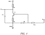
- FIG. 4 is a schematic structural diagram of the second functional interface circuit 120.
- the second functional interface circuit 120 includes the third capacitor C3, a third resistor R3, a first triode T1, a fourth resistor R4, the sixth resistor R6, and the tenth resistor R10.
- the first end of the third capacitor C3 is connected to the external port P1, the second end of the third capacitor C3 is connected to the first end of the sixth resistor R6, a first end of the third resistor R3 is connected to a second reference power supply REF2, a second end of the third resistor R3 is connected to the external port P1, a collector of the first triode T1 is connected to the second end of the third resistor R3, a base of the first triode T1 is connected to the second end of the sixth resistor R6, an emitter of the first triode T1 is connected to a first end of the fourth resistor R4, a second end of the fourth resistor R4 is connected to the second end of the third capacitor C3 and to ground GND5, the first end of the tenth resistor R10 is connected to the base of the first triode T1, and the second end of the tenth resistor R10 is connected to the second port P3 (e.g., the general-purpose input/output (GPIO) interface) of the processor.
- a level of the external port P1 will vary reversely with a level of the output port P3 of the processor. That is, when the port P3 is at a high level, the external port P1 presents a low level, and when the port P3 is at a low level, the external port P1 presents a high level. For example, when the port P3 is at a low level, the first triode T1 is turned off, and a voltage at the P1 port is approximately equal to the second reference voltage REF2 (i.e., about 5 V), and is thus at a high level.
- the second reference voltage REF2 i.e., about 5 V
- circuit elements in the second functional interface circuit shown in FIG. 4 partially overlap the circuit elements in the first functional interface circuit shown in FIG. 3 .
- the overlapping elements include the third capacitor C3, the sixth resistor R6, and the tenth resistor R10.
- the second functional interface circuit 120 is configured to implement a function of "forward output" and to be adapted to the output port of the processor 150.
- FIG. 5 is another schematic structural diagram of the second functional interface circuit 120.
- the second functional interface circuit 120 includes the third capacitor C3, the fifth resistor R5, the sixth resistor R6, a seventh resistor R7, an eighth resistor R8, a second triode T2, a third triode T3, and a ninth resistor R9.
- the first end of the third capacitor C3 is connected to the external port P1, the second end of the third capacitor C3 is connected to the first end of the sixth resistor R6 and to the ground GND5, the first end of the fifth resistor R5 is connected to the external port P1, the second end of the fifth resistor R5 is connected to the second end of the sixth resistor R6, a first end of the seventh resistor R7 is connected to a third reference power supply REF3, a second end of the seventh resistor R7 is connected to an emitter of the second triode T2, a first end of the eighth resistor R8 is connected to the third reference power supply REF3, a second end of the eighth resistor R8 is connected to a base of the second triode T2, a collector of the second triode T2 is connected to the second end of the sixth resistor R6, a collector of the third triode T3 is connected to the base of the second triode T2, a base of the third triode T3 is connected to a first end of the ninth resistor R9, an emitter of
- the level of the external port P1 will vary in the same way as the level of the output port P3 of the processor. That is, when the port P3 is at a high level, the external port P1 presents a high level, and when the port P3 is at a low level, the external port P1 presents a low level.
- the second triode T2 and the third triode T3 are turned off, and the voltage at the P1 port is approximately equal to a voltage at the P3 port, and is thus at a low level.
- the second triode T2 and the third triode T3 are turned on, and the voltage at the external port P1 is approximately equal to the voltage at the port P3 (i.e., at a high level).
- circuit elements in the second functional interface circuit shown in FIG. 5 partially overlap the circuit elements in the first functional interface circuit shown in FIG. 3 .
- the overlapping elements include the third capacitor C3, the fifth resistor R5, and the sixth resistor R6.
- FIG. 6 is a schematic structural diagram of an integrated interface circuit according to one embodiment of the present invention.
- the integrated interface circuit includes the third functional interface circuit 130 shown in FIG. 2 , the first functional interface circuit 110 shown in FIG. 3 , and the second functional interface circuit 120 shown in FIGs 4 and 5 .
- the integrated interface circuit includes a plurality of functional interface circuits respectively corresponding to different functions, such as the first functional interface circuit 110, the second functional interface circuit 120, and the third functional interface circuit 130.
- the external port P1 may correspond to the plurality of functional interface circuits. That is, through (adaptation of) the plurality of functional interface circuits, the external port P1 may obtain a plurality of integrated functions, such that limited port resources are advantageously saved.
- the integrated interface circuit multiplexes circuit elements in different functional interface circuits, which makes the overall integrated interface circuit more simplified and reduces manufacturing costs.
- the above integrated interface circuit may further include a selector configured to select a corresponding functional interface circuit from the plurality of functional interface circuits according to a control signal.
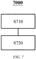
- FIG. 7 is a schematic diagram of a method 7000 for manufacturing an interface circuit according to one embodiment of the present invention.
- the method 7000 for manufacturing an interface circuit includes the steps as follows: in step S710, determining a function corresponding to the interface circuit; and in step S720, selecting, based on the determined function and from the above integrated interface circuit, a corresponding functional interface circuit for filling.
- determining the function corresponding to the interface circuit in step S710 may be implemented by receiving an external control signal. Further, after the function is determined, the corresponding functional interface circuit is selected for filling. For example, when it is determined that the interface circuit corresponds to an ADC function, the circuit elements (i.e., the first inductor L1, the first resistor R1, the first diode D1, the first capacitor C1, the second resistor R2, and the second capacitor C2 that are shown in FIG. 2 ) of the third functional interface circuit are selected for filling.
- the circuit elements i.e., the first inductor L1, the first resistor R1, the first diode D1, the first capacitor C1, the second resistor R2, and the second capacitor C2 that are shown in FIG. 2
- the integrated interface circuit may be located in an electronic control unit (ECU) as an example.
- ECU electronice control unit
- the external port When the integrated interface circuit is applied in the electronic control unit (ECU), the external port may be a port through which the ECU is connected to the outside, and the processor may be a microprocessor of the ECU.
- the integrated interface circuit includes a plurality of functional interface circuits respectively corresponding to different functions, such as the first functional interface circuit and the second functional interface circuit. In this manner, the external port may correspond to the plurality of functional interface circuits.
- the external port may obtain a plurality of integrated functions, such that limited port resources are advantageously saved.
- arranging the integrated interface circuit 1000 in the electronic control unit (ECU) may enable the electronic control unit (ECU) to have more port resources to meet customized requirements.
Landscapes
- Engineering & Computer Science (AREA)
- Theoretical Computer Science (AREA)
- General Engineering & Computer Science (AREA)
- Physics & Mathematics (AREA)
- General Physics & Mathematics (AREA)
- Computer Hardware Design (AREA)
- Automation & Control Theory (AREA)
- Semiconductor Integrated Circuits (AREA)
- Logic Circuits (AREA)
- Communication Control (AREA)
Abstract
Description
- The present invention relates to an interface circuit design, and more specifically to an integrated interface circuit, to a method for manufacturing an interface circuit, to an electronic control unit, to a vehicle, and to a computer storage medium.
- A processing unit in an existing electronic control unit (ECU) of an electric vehicle generally has a plurality of ports with different functions, such as an analogue-to-digital converter (ADC) port, an input pin port, an output pin port, and a ground port. Each functional port has a certain requirement for a specification of an input signal or an output signal, for example, an input voltage is required not to be higher than 4 V, etc.
- If the external ports of the ECU are allocated by function (i.e., each external port corresponds to a single function), available external port resources of the ECU will be so tight that no more ports can be set for customized requirements.
- According to an aspect of the present invention, there is provided an integrated interface circuit, which includes: a plurality of functional interface circuits which are connected between an external port and a processor and respectively correspond to different functions, wherein the plurality of functional interface circuits include a first functional interface circuit corresponding to a first function and a second functional interface circuit corresponding to a second function, and circuit elements in the second functional interface circuit at least partially overlap circuit elements in the first functional interface circuit.
- Optionally, in the above integrated interface circuit, the plurality of functional interface circuits further include a third functional interface circuit corresponding to a third function, wherein circuit elements in the third functional interface circuit do not overlap the circuit elements in either the first functional interface circuit or the second functional interface circuit.
- Optionally, in the above integrated interface circuit, the external port is an external input port for receiving an external input signal or an external output interface for transmitting a signal to the outside.
- Optionally, in the above integrated interface circuit, the processor is a single-chip microcomputer.
- Optionally, in the above integrated interface circuit, the third functional interface circuit includes: a first filtering element configured to filter an external input signal received from the external port; a voltage dividing element connected in series with the first filtering element and configured to reduce a voltage of the external input signal filtered by the first filtering element; and a voltage limiting element, wherein one end of the voltage limiting element is connected in series with the voltage dividing element and the other end of the voltage limiting element is connected in series with a corresponding terminal of the processor, and the voltage limiting element is configured to limit a voltage output to the corresponding terminal of the processor.
- Optionally, in the above integrated interface circuit, the third functional interface circuit further includes: a second filtering element connected in series with the voltage dividing element and the voltage limiting element and configured to perform second-stage filtering on the external input signal experiencing voltage dividing by the voltage dividing element.
- Optionally, in the above integrated interface circuit, the third functional interface circuit includes: the first filtering element including a first inductor and a first capacitor, wherein a first end of the first inductor is connected to the external port, a second end of the first inductor is connected to a first end of the capacitor, and a second end of the capacitor is connected to ground; the voltage dividing element including a first resistor and a second resistor, wherein a first end of the first resistor is connected to the second end of the first inductor, a second end of the first resistor is connected to a first end of the second resistor, and a second end of the second resistor is connected to ground; the second filtering element including a second capacitor, wherein a first end of the second capacitor is connected to the second end of the first resistor, and a second end of the second capacitor is connected to ground; and the voltage limiting element including a first diode, wherein a first end of the first diode is connected to the first end of the second capacitor, a second end of the first diode is connected to a first reference power supply, and a first port of the processor is connected to the first end of the first diode.
- Optionally, in the above integrated interface circuit, the first functional interface circuit includes: a third capacitor, wherein a first end of the third capacitor is connected to the external port, and a second end of the third capacitor is connected to a first end of a sixth resistor; a fifth resistor, wherein a first end of the fifth resistor is connected to the external port, and a second end of the fifth resistor is connected to a second end of the sixth resistor; the sixth resistor; and a tenth resistor, wherein a first end of the tenth resistor is connected to the second end of the fifth resistor, and a second end of the tenth resistor is connected to a second port of the processor.
- Optionally, in the above integrated interface circuit, the elements in the second functional interface circuit that overlap those in the first functional interface circuit include the third capacitor, the sixth resistor, and the tenth resistor.
- Optionally, in the above integrated interface circuit, the second functional interface circuit includes: the third capacitor, wherein the first end of the third capacitor is connected to the external port, and the second end of the third capacitor is connected to the first end of the sixth resistor; a third resistor, wherein a first end of the third resistor is connected to a second reference power supply, and a second end of the third resistor is connected to the external port; a first triode, wherein a collector of the first triode is connected to the second end of the third resistor, a base of the first triode is connected to the second end of the sixth resistor, and an emitter of the first triode is connected to a first end of a fourth resistor; the fourth resistor, wherein a second end of the fourth resistor is connected to the second end of the third capacitor and to ground; the sixth resistor; and the tenth resistor, wherein the first end of the tenth resistor is connected to the base of the first triode, and the second end of the tenth resistor is connected to the second port of the processor.
- Optionally, in the above integrated interface circuit, the elements in the second functional interface circuit that overlap those in the first functional interface circuit include the third capacitor, the fifth resistor, and the sixth resistor.
- Optionally, in the above integrated interface circuit, the second functional interface circuit includes: the third capacitor, wherein the first end of the third capacitor is connected to the external port, and the second end of the third capacitor is connected to the first end of the sixth resistor; the fifth resistor, wherein the first end of the fifth resistor is connected to the external port, and the second end of the fifth resistor is connected to the second end of the sixth resistor; the sixth resistor; a seventh resistor, wherein a first end of the seventh resistor is connected to a third reference power supply, and a second end of the seventh resistor is connected to an emitter of a second triode; an eighth resistor, wherein a first end of the eighth resistor is connected to the third reference power supply, and a second end of the eighth resistor is connected to a base of the second triode; the second triode, wherein a collector of the second triode is connected to the second end of the sixth resistor; a third triode, wherein a collector of the third triode is connected to the base of the second triode, a base of the third triode is connected to a first end of a ninth resistor, and an emitter of the third triode is connected to ground; and the ninth resistor, wherein a second end of the ninth resistor is connected to the second end of the sixth resistor, and the second end of the ninth resistor is further connected to the second port of the processor.
- Optionally, the above integrated interface circuit further includes: a selector configured to select a corresponding functional interface circuit from the plurality of functional interface circuits according to a control signal.
- According to another aspect of the present invention, there is provided a method for manufacturing an interface circuit, the method including: determining a function corresponding to the interface circuit; and selecting, based on the determined function and from the above integrated interface circuit, a corresponding functional interface circuit for filling.
- According to yet another aspect of the present invention, there is provided an electronic control unit including the integrated interface circuit as described above.
- According to yet another aspect of the present invention, there is provided a vehicle including the electronic control unit described above.
- According to yet another aspect of the present invention, there is provided a computer storage medium including instructions, wherein, when the instructions are run, the method as described above is performed.
- The integrated interface circuit of the present invention includes a plurality of functional interface circuits which are connected between an external port and a processor and respectively correspond to different functions. In this manner, a single external port may correspond to the plurality of functional interface circuits. That is, through adaptation of the plurality of functional interface circuits, the single external port may obtain a plurality of functions (integrated functions) provided by the functional interface circuits or the processor, such that limited port resources are advantageously saved (i.e., there are more port resources to meet customized requirements). In addition, there may be at least partially overlapping circuit elements between different functional interface circuits, which makes the overall integrated interface circuit more simplified and reduces manufacturing costs.
- The above and other objects and advantages of the present invention will be more complete and clearer from the following detailed description in conjunction with the accompanying drawings, wherein the same or similar elements are denoted by the same reference numerals.
-
FIG. 1 is a schematic diagram of an integrated interface circuit according to an embodiment of the present invention; -
FIG. 2 is a schematic structural diagram of a third functional interface circuit according to an embodiment of the present invention; -
FIG. 3 is a schematic structural diagram of a first functional interface circuit according to an embodiment of the present invention; -
FIG. 4 is a schematic structural diagram of a second functional interface circuit according to an embodiment of the present invention; -
FIG. 5 is a schematic structural diagram of a second functional interface circuit according to another embodiment of the present invention; -
FIG. 6 is a schematic structural diagram of an integrated interface circuit according to an embodiment of the present invention; and -
FIG. 7 is a schematic diagram of a method for manufacturing an interface circuit according to an embodiment of the present invention. - It should be understood that the term "vehicle" or another similar term used herein includes various motor vehicles and non-motor vehicles, such as passenger vehicles (including sport utility vehicles, buses, trucks, etc.), various commercial vehicles, ships, aircraft, motorcycles, and bicycles, and includes hybrid vehicles, electric vehicles, etc. A hybrid vehicle is a vehicle with two or more power sources, such as a vehicle powered by a gasoline engine and an electric motor.
- Although exemplary embodiments are described as using a plurality of units to perform exemplary processes, it should be understood that these exemplary processes may also be performed by one or more modules.
- Moreover, control logic of the disclosure may be included on a computer-readable medium as executable program instructions, which are implemented by a processor or the like. Examples of the computer-readable medium include, but are not limited to, a ROM, a RAM, an optical disc, a magnetic tape, a floppy disk, a flash drive, a smart card, and an optical data storage apparatus. A computer-readable recording medium may also be distributed in a computer system connected to a network, so that the computer-readable medium is stored and implemented in a distributed manner, for example, through a vehicle telematics service or a controller area network (CAN).
- Unless specifically mentioned or obvious from context, as used herein, the term "approximately" is understood to be within a range of normal tolerance in the art, for example, within two standard deviations of a mean.
- An integrated interface circuit according to various exemplary embodiments of the present invention will be described below in detail with reference to the accompanying drawings.
-
FIG. 1 is a schematic diagram of an integratedinterface circuit 1000 according to an embodiment of the present invention. As shown inFIG. 1 , theintegrated interface circuit 1000 includes a plurality of functional interface circuits which are connected between anexternal port 140 and aprocessor 150 and respectively correspond to different functions. The plurality of functional interface circuits include a firstfunctional interface circuit 110 corresponding to a first function and a secondfunctional interface circuit 120 corresponding to a second function, and circuit elements in the secondfunctional interface circuit 120 at least partially overlap circuit elements in the firstfunctional interface circuit 110. - In the context of the present invention, the term "interface circuit" represents a logic circuit that serves as a link between an external device/external port and an internal processor and is a bridge for information exchange between the processor and the external device. Functions of the interface circuit include, but are not limited to, level connection, impedance matching, signal processing or "maintenance", electrostatic protection, alternating current/direct current isolation, etc.
- According to different corresponding functions, the interface circuit can be further subdivided into different functional interface circuits, namely, a first functional interface circuit, a second functional interface circuit, etc. As an example, the interface circuit is classified according to different functions implemented by the interface circuit. As another example, the interface circuit is classified according to different ports matching the processor. As yet another example, according to both functions implemented by the interface circuit and functions implemented by the processor, the interface circuit is classified by different adapted or implemented functions.
- In the context of the present invention, the term "external port" refers to a port connected to an external device, which may be an external input port for receiving an external input signal, or an external output interface for transmitting a signal to the outside. The "processor" may be any unit that performs a processing function, such as a single-chip microcomputer. Those skilled in the art can appreciate that the processor may provide a plurality of functions, such as various functions of signal processing and analogue-to-digital conversion. In addition, the processor may have a plurality of ports, and the different ports each have a certain specification requirement for an input or output signal. When the
integrated interface circuit 1000 is applied in an electronic control unit (ECU), theexternal port 140 may be a port through which the ECU is connected to the outside, and theprocessor 150 may be a microprocessor of the ECU. - The
integrated interface circuit 1000 includes the plurality of functional interface circuits respectively corresponding to different functions, such as the firstfunctional interface circuit 110 and the secondfunctional interface circuit 120. In this manner, theexternal port 140 may correspond to the plurality of functional interface circuits. That is, through (adaptation of) the plurality of functional interface circuits, theexternal port 140 may obtain a plurality of integrated functions, such that limited port resources are advantageously saved. In other words, arranging theintegrated interface circuit 1000 in the electronic control unit (ECU) may enable the electronic control unit (ECU) to have more port resources to meet customized requirements. In addition, the circuit elements in the secondfunctional interface circuit 120 at least partially overlap the circuit elements in the firstfunctional interface circuit 110, which makes the overall integratedinterface circuit 1000 more simplified and reduces manufacturing costs. - In some embodiments, with continued reference to
FIG. 1 , in the aboveintegrated interface circuit 1000, the plurality of functional interface circuits may further include a third functional interface circuit 130 (shown with dashed lines) for implementing a third function. Circuit elements in the thirdfunctional interface circuit 130 do not overlap the circuit elements in either the firstfunctional interface circuit 110 or the secondfunctional interface circuit 120. Those skilled in the art can appreciate that more or fewer functional interface circuits may be arranged in theintegrated interface circuit 1000 as needed, and these functional interface circuits may at least partially overlap the firstfunctional interface circuit 110, the secondfunctional interface circuit 120, and the thirdfunctional interface circuit 130, or may not overlap any of the above. - In one embodiment, the third
functional interface circuit 130 corresponds to an analogue-to-digital conversion (ADC) input port of theprocessor 150. The thirdfunctional interface circuit 130 may include a first filtering element, a voltage dividing element, and a voltage limiting element. The first filtering element is configured to filter an external input signal received from the external port; the voltage dividing element is configured to be connected in series with the first filtering element, and is configured to reduce a voltage of the external input signal filtered by the first filtering element; and one end of the voltage limiting element is connected in series with the voltage dividing element, the other end of the voltage limiting element is connected in series with a corresponding terminal of the processor, and the voltage limiting element is configured to limit a voltage output to the corresponding terminal of the processor. In some embodiments, the third functional interface circuit may further include: a second filtering element connected in series with the voltage dividing element and the voltage limiting element and configured to perform second-stage filtering on the external input signal experiencing voltage dividing by the voltage dividing element. -
FIG. 2 is a schematic structural diagram of the thirdfunctional interface circuit 130 configured to be adapted to the ADC input port of theprocessor 150. As shown inFIG. 2 , the thirdfunctional interface circuit 130 includes: the first filtering element composed of a first inductor L1 and a first capacitor C1, the voltage dividing element composed of a first resistor R1 and a second resistor R2, the second filtering element composed of a second capacitor C2, and the voltage limiting element composed of a first diode D1. Certainly, those skilled in the art can appreciate that the filtering elements, the voltage dividing element, and the voltage limiting element described above may include more circuit elements according to actual needs, and are not limited to the specific circuit inFIG. 2 . - With continued reference to
FIG. 2 , a first end of the first inductor L1 is connected to an external port P1, a second end of the first inductor L1 is connected to a first end of the first capacitor C1, a second end of the first capacitor C1 is connected to ground GND1, a first end of the first resistor R1 is connected to the second end of the first inductor L1, a second end of the first resistor R1 is connected to a first end of the second resistor R2, a second end of the second resistor R2 is connected to ground GND2, a first end of the second capacitor C2 is connected to the second end of the first resistor R1, a second end of the second capacitor C2 is connected to ground GND3, a first end of the first diode D1 is connected to the first end of the second capacitor C2, a second end of the first diode D1 is connected to a first reference power supply REF1, and a port P2 (i.e., the ADC input port) of the processor is connected to the first end of the first diode D1. - Through the functional interface circuit as shown in
FIG. 2 , the first inductor L1 and the first capacitor C1 constitute an LC filtering element (i.e., the first filtering element). After filtering through the first inductor L1 and the first capacitor C1, a smooth direct current may be obtained, reducing a ripple voltage. Moreover, this filtering may also achieve a good filtering effect when a current fluctuates with changes. The voltage dividing element composed of the first resistor R1 and the second resistor R2 can reduce a voltage of an external input signal experiencing the LC filtering. Appropriate resistance values of the first resistor R1 and the second resistor R2 may be set as needed, such that a desired output voltage at the port P2 may be obtained. In addition, the second filtering element composed of C2 is configured to perform capacitance filtering (i.e., secondary filtering) on a signal output to the port P2, such that clutter interference may be further reduced. In addition, since a voltage of the first reference power supply is 3.3 V and a turnon voltage of the first diode D1 is 0.7 V, a voltage of the port P2 is clamped below 4 V. Those skilled in the art can appreciate that setting the voltage of the first reference power supply at different values enables the voltage of the port P2 to be clamped below corresponding different voltage values. - In one embodiment, the first
functional interface circuit 110 is configured to be adapted to an input port of theprocessor 150.FIG. 3 is a schematic structural diagram of the firstfunctional interface circuit 110 which is adapted to the input port. As shown inFIG. 3 , the firstfunctional interface circuit 110 includes a third capacitor C3, a fifth resistor R5, a sixth resistor R6, and a tenth resistor R10. A first end of the third capacitor C3 is connected to the external port P1, a second end of the third capacitor C3 is connected to a first end of the sixth resistor R6, a first end of the fifth resistor R5 is connected to the external port P1, a second end of the fifth resistor R5 is connected to a second end of the sixth resistor R6, a first end of the tenth resistor R10 is connected to the second end of the fifth resistor R5, and a second end of the tenth resistor R10 is connected to a second port P3 (e.g., a general-purpose input/output (GPIO) interface) of the processor. The firstfunctional interface circuit 110 shown inFIG. 3 can function readily in current limiting by reasonably setting capacitance and resistance values of each circuit element. For example, when an input at the P1 port is a low-frequency signal (e.g., a direct current signal), due to the presence of the third capacitor C3, a direct current does not flow through a branch formed by the third capacitor C3 and the sixth resistor R6, but only flows through the fifth resistor R5 and the tenth resistor R10. Assuming that the fifth resistor has a high resistance, the current output to the port P3 is readily limited. - In one embodiment, the second
functional interface circuit 120 is configured to implement a function of "reverse output" and to be adapted to an output port of theprocessor 150. -
FIG. 4 is a schematic structural diagram of the secondfunctional interface circuit 120. As shown inFIG. 4 , the secondfunctional interface circuit 120 includes the third capacitor C3, a third resistor R3, a first triode T1, a fourth resistor R4, the sixth resistor R6, and the tenth resistor R10. The first end of the third capacitor C3 is connected to the external port P1, the second end of the third capacitor C3 is connected to the first end of the sixth resistor R6, a first end of the third resistor R3 is connected to a second reference power supply REF2, a second end of the third resistor R3 is connected to the external port P1, a collector of the first triode T1 is connected to the second end of the third resistor R3, a base of the first triode T1 is connected to the second end of the sixth resistor R6, an emitter of the first triode T1 is connected to a first end of the fourth resistor R4, a second end of the fourth resistor R4 is connected to the second end of the third capacitor C3 and to ground GND5, the first end of the tenth resistor R10 is connected to the base of the first triode T1, and the second end of the tenth resistor R10 is connected to the second port P3 (e.g., the general-purpose input/output (GPIO) interface) of the processor. - Through the circuit in
FIG. 4 , a level of the external port P1 will vary reversely with a level of the output port P3 of the processor. That is, when the port P3 is at a high level, the external port P1 presents a low level, and when the port P3 is at a low level, the external port P1 presents a high level. For example, when the port P3 is at a low level, the first triode T1 is turned off, and a voltage at the P1 port is approximately equal to the second reference voltage REF2 (i.e., about 5 V), and is thus at a high level. When the port P3 is at a high level, the first triode T1 is turned on, the fourth resistor R4 is connected in parallel to the sixth resistor R6, and an equivalent resistance value thereof is not comparable with those of the third resistor R3 and the tenth resistor R10. Therefore, a voltage divided on the external port P1 is very low (i.e., at a low level). - In addition, it should be noted that the circuit elements in the second functional interface circuit shown in
FIG. 4 partially overlap the circuit elements in the first functional interface circuit shown inFIG. 3 . The overlapping elements include the third capacitor C3, the sixth resistor R6, and the tenth resistor R10. - In one embodiment, the second
functional interface circuit 120 is configured to implement a function of "forward output" and to be adapted to the output port of theprocessor 150. -
FIG. 5 is another schematic structural diagram of the secondfunctional interface circuit 120. As shown inFIG. 5 , the secondfunctional interface circuit 120 includes the third capacitor C3, the fifth resistor R5, the sixth resistor R6, a seventh resistor R7, an eighth resistor R8, a second triode T2, a third triode T3, and a ninth resistor R9. The first end of the third capacitor C3 is connected to the external port P1, the second end of the third capacitor C3 is connected to the first end of the sixth resistor R6 and to the ground GND5, the first end of the fifth resistor R5 is connected to the external port P1, the second end of the fifth resistor R5 is connected to the second end of the sixth resistor R6, a first end of the seventh resistor R7 is connected to a third reference power supply REF3, a second end of the seventh resistor R7 is connected to an emitter of the second triode T2, a first end of the eighth resistor R8 is connected to the third reference power supply REF3, a second end of the eighth resistor R8 is connected to a base of the second triode T2, a collector of the second triode T2 is connected to the second end of the sixth resistor R6, a collector of the third triode T3 is connected to the base of the second triode T2, a base of the third triode T3 is connected to a first end of the ninth resistor R9, an emitter of the third triode T3 is connected to ground GND4, a second end of the ninth resistor R9 is connected to the second end of the sixth resistor R6, and the second end of the ninth resistor R9 is further connected to the second port P3 (e.g., the general-purpose input/output (GPIO) interface) of the processor. - Through the circuit in
FIG. 5 , the level of the external port P1 will vary in the same way as the level of the output port P3 of the processor. That is, when the port P3 is at a high level, the external port P1 presents a high level, and when the port P3 is at a low level, the external port P1 presents a low level. For example, when the port P3 is at a low level, the second triode T2 and the third triode T3 are turned off, and the voltage at the P1 port is approximately equal to a voltage at the P3 port, and is thus at a low level. When the port P3 is at a high level, the second triode T2 and the third triode T3 are turned on, and the voltage at the external port P1 is approximately equal to the voltage at the port P3 (i.e., at a high level). - In addition, it should be noted that the circuit elements in the second functional interface circuit shown in
FIG. 5 partially overlap the circuit elements in the first functional interface circuit shown inFIG. 3 . The overlapping elements include the third capacitor C3, the fifth resistor R5, and the sixth resistor R6. -
FIG. 6 is a schematic structural diagram of an integrated interface circuit according to one embodiment of the present invention. The integrated interface circuit includes the thirdfunctional interface circuit 130 shown inFIG. 2 , the firstfunctional interface circuit 110 shown inFIG. 3 , and the secondfunctional interface circuit 120 shown inFIGs 4 and5 . The integrated interface circuit includes a plurality of functional interface circuits respectively corresponding to different functions, such as the firstfunctional interface circuit 110, the secondfunctional interface circuit 120, and the thirdfunctional interface circuit 130. In this manner, the external port P1 may correspond to the plurality of functional interface circuits. That is, through (adaptation of) the plurality of functional interface circuits, the external port P1 may obtain a plurality of integrated functions, such that limited port resources are advantageously saved. In addition, the integrated interface circuit multiplexes circuit elements in different functional interface circuits, which makes the overall integrated interface circuit more simplified and reduces manufacturing costs. - Although not shown in
FIG. 6 , in some embodiments, the above integrated interface circuit may further include a selector configured to select a corresponding functional interface circuit from the plurality of functional interface circuits according to a control signal. -
FIG. 7 is a schematic diagram of amethod 7000 for manufacturing an interface circuit according to one embodiment of the present invention. As shown inFIG. 7 , themethod 7000 for manufacturing an interface circuit includes the steps as follows:
in step S710, determining a function corresponding to the interface circuit; and in step S720, selecting, based on the determined function and from the above integrated interface circuit, a corresponding functional interface circuit for filling. - In some embodiments, determining the function corresponding to the interface circuit in step S710 may be implemented by receiving an external control signal. Further, after the function is determined, the corresponding functional interface circuit is selected for filling. For example, when it is determined that the interface circuit corresponds to an ADC function, the circuit elements (i.e., the first inductor L1, the first resistor R1, the first diode D1, the first capacitor C1, the second resistor R2, and the second capacitor C2 that are shown in
FIG. 2 ) of the third functional interface circuit are selected for filling. - The integrated interface circuit may be located in an electronic control unit (ECU) as an example. The so-called "electronic control unit", also referred to as a "trip computer", a "vehicle-mounted computer", etc., is a vehicle-dedicated microcomputer controller in terms of use. When the integrated interface circuit is applied in the electronic control unit (ECU), the external port may be a port through which the ECU is connected to the outside, and the processor may be a microprocessor of the ECU. The integrated interface circuit includes a plurality of functional interface circuits respectively corresponding to different functions, such as the first functional interface circuit and the second functional interface circuit. In this manner, the external port may correspond to the plurality of functional interface circuits. That is, through (adaptation of) the plurality of functional interface circuits, the external port may obtain a plurality of integrated functions, such that limited port resources are advantageously saved. In other words, arranging the
integrated interface circuit 1000 in the electronic control unit (ECU) may enable the electronic control unit (ECU) to have more port resources to meet customized requirements. - The above examples mainly illustrate the integrated interface circuit of the present invention. Although only some of the implementations of the present invention have been described, those of ordinary skill in the art should understand that the present invention can be implemented in many other forms without departing from its spirit and scope. For example, the reference power supplies are set to different voltage values according to actual needs. Therefore, the presented examples and implementations are considered to be schematic rather than restrictive, and without departing from the spirit and scope of the present invention that are defined by the claims; the present invention may cover various changes and replacements.
Claims (17)
- Integrated interface circuit, characterized in that it comprises:a plurality of functional interface circuits which are connected between an external port and a processor and respectively correspond to different functions,wherein the plurality of functional interface circuits comprise a first functional interface circuit corresponding to a first function and a second functional interface circuit corresponding to a second function, and circuit elements in the second functional interface circuit at least partially overlap circuit elements in the first functional interface circuit.
- Integrated interface circuit according to Claim 1, wherein the plurality of functional interface circuits further comprise a third functional interface circuit corresponding to a third function, wherein circuit elements in the third functional interface circuit do not overlap the circuit elements in either the first functional interface circuit or the second functional interface circuit.
- Integrated interface circuit according to Claim 1, wherein the external port is an external input port for receiving an external input signal, or an external output interface for transmitting a signal to the outside.
- Integrated interface circuit according to Claim 1, wherein the processor is a single-chip microcomputer.
- Integrated interface circuit according to Claim 2, wherein the third functional interface circuit comprises:a first filtering element configured to filter an external input signal received from the external port;a voltage dividing element connected in series with the first filtering element and configured to reduce a voltage of the external input signal filtered by the first filtering element; anda voltage limiting element, wherein one end of the voltage limiting element is connected in series with the voltage dividing element and the other end of the voltage limiting element is connected in series with a corresponding terminal of the processor, and the voltage limiting element is configured to limit a voltage output to the corresponding terminal of the processor.
- Integrated interface circuit according to Claim 5, wherein the third functional interface circuit further comprises:
a second filtering element connected in series with the voltage dividing element and the voltage limiting element and configured to perform second-stage filtering on the external input signal experiencing voltage dividing by the voltage dividing element. - Integrated interface circuit according to Claim 6, wherein the third functional interface circuit comprises:the first filtering element including a first inductor and a first capacitor, wherein a first end of the first inductor is connected to the external port, a second end of the first inductor is connected to a first end of the capacitor, and a second end of the capacitor is connected to ground;the voltage dividing element including a first resistor and a second resistor, wherein a first end of the first resistor is connected to the second end of the first inductor, a second end of the first resistor is connected to a first end of the second resistor, and a second end of the second resistor is connected to ground;the second filtering element including a second capacitor, wherein a first end of the second capacitor is connected to the second end of the first resistor, and a second end of the second capacitor is connected to ground; andthe voltage limiting element including a first diode, wherein a first end of the first diode is connected to the first end of the second capacitor, a second end of the first diode is connected to a first reference power supply, and a first port of the processor is connected to the first end of the first diode.
- Integrated interface circuit according to Claim 1, wherein the first functional interface circuit comprises:a third capacitor, wherein a first end of the third capacitor is connected to the external port, and a second end of the third capacitor is connected to a first end of a sixth resistor;a fifth resistor, wherein a first end of the fifth resistor is connected to the external port, and a second end of the fifth resistor is connected to a second end of the sixth resistor;the sixth resistor; anda tenth resistor, wherein a first end of the tenth resistor is connected to the second end of the fifth resistor, and a second end of the tenth resistor is connected to a second port of the processor.
- Integrated interface circuit according to Claim 8, wherein the elements in the second functional interface circuit that overlap those in the first functional interface circuit comprise the third capacitor, the sixth resistor, and the tenth resistor.
- Integrated interface circuit according to Claim 9, wherein the second functional interface circuit comprises:the third capacitor, wherein the first end of the third capacitor is connected to the external port, and the second end of the third capacitor is connected to the first end of the sixth resistor;a third resistor, wherein a first end of the third resistor is connected to a second reference power supply, and a second end of the third resistor is connected to the external port;a first triode, wherein a collector of the first triode is connected to the second end of the third resistor, a base of the first triode is connected to the second end of the sixth resistor, and an emitter of the first triode is connected to a first end of a fourth resistor;the fourth resistor, wherein a second end of the fourth resistor is connected to the second end of the third capacitor and to ground;the sixth resistor; andthe tenth resistor, wherein the first end of the tenth resistor is connected to the base of the first triode, and the second end of the tenth resistor is connected to the second port of the processor.
- Integrated interface circuit according to Claim 8, wherein the elements in the second functional interface circuit that overlap those in the first functional interface circuit comprise the third capacitor, the fifth resistor, and the sixth resistor.
- Integrated interface circuit according to Claim 11, wherein the second functional interface circuit comprises:the third capacitor, wherein the first end of the third capacitor is connected to the external port, and the second end of the third capacitor is connected to the first end of the sixth resistor;the fifth resistor, wherein the first end of the fifth resistor is connected to the external port, and the second end of the fifth resistor is connected to the second end of the sixth resistor;the sixth resistor;a seventh resistor, wherein a first end of the seventh resistor is connected to a third reference power supply, and a second end of the seventh resistor is connected to an emitter of a second triode;an eighth resistor, wherein a first end of the eighth resistor is connected to the third reference power supply, and a second end of the eighth resistor is connected to a base of the second triode;the second triode, wherein a collector of the second triode is connected to the second end of the sixth resistor;a third triode, wherein a collector of the third triode is connected to the base of the second triode, a base of the third triode is connected to a first end of a ninth resistor, and an emitter of the third triode is connected to ground; andthe ninth resistor, wherein a second end of the ninth resistor is connected to the second end of the sixth resistor, and the second end of the ninth resistor is further connected to the second port of the processor.
- Integrated interface circuit according to Claim 1 or 2, wherein the integrated interface circuit further comprises:
a selector configured to select a corresponding functional interface circuit from the plurality of functional interface circuits according to a control signal. - Method for manufacturing an interface circuit, characterized in that it includes:determining a function corresponding to the interface circuit; andselecting, based on the determined function and from the integrated interface circuit according to any one of Claims 1 to 13, a corresponding functional interface circuit for filling.
- Electronic control unit, comprising the integrated interface circuit according to any one of Claims 1 to 13.
- Vehicle, comprising the electronic control unit according to Claim 15.
- Computer storage medium, characterized in that it comprises instructions, wherein, when the instructions are run, the method according to Claim 14 is performed.
Applications Claiming Priority (2)
| Application Number | Priority Date | Filing Date | Title |
|---|---|---|---|
| CN202010104147.0A CN113282526B (en) | 2020-02-20 | 2020-02-20 | Integrated interface circuit and method for manufacturing the same |
| PCT/CN2021/076175 WO2021164637A1 (en) | 2020-02-20 | 2021-02-09 | Integrated interface circuit and interface circuit manufacturing method |
Publications (3)
| Publication Number | Publication Date |
|---|---|
| EP4109284A1 true EP4109284A1 (en) | 2022-12-28 |
| EP4109284A4 EP4109284A4 (en) | 2024-03-27 |
| EP4109284B1 EP4109284B1 (en) | 2025-12-31 |
Family
ID=77275016
Family Applications (1)
| Application Number | Title | Priority Date | Filing Date |
|---|---|---|---|
| EP21757503.4A Active EP4109284B1 (en) | 2020-02-20 | 2021-02-09 | INTEGRATED INTERFACE SWITCHING AND METHOD FOR ESTABLISHING AN INTERFACE SWITCHING |
Country Status (4)
| Country | Link |
|---|---|
| EP (1) | EP4109284B1 (en) |
| CN (1) | CN113282526B (en) |
| TW (1) | TWI788784B (en) |
| WO (1) | WO2021164637A1 (en) |
Family Cites Families (8)
| Publication number | Priority date | Publication date | Assignee | Title |
|---|---|---|---|---|
| JP3956527B2 (en) * | 1999-03-26 | 2007-08-08 | 株式会社デンソー | Voltage output device |
| US8656065B1 (en) * | 2013-01-29 | 2014-02-18 | Honeywell International Inc. | Method and apparatus for automatically selecting a plurality of modes for programmable interface circuit by coupling field devices to process controllers |
| CN203896318U (en) * | 2014-05-13 | 2014-10-22 | 联合汽车电子有限公司 | Differential input circuit |
| CN105528270B (en) * | 2015-12-30 | 2018-03-30 | 东风商用车有限公司 | JTAG (Joint test action group) and BDM (brain-based data model) integrated debugging interface and using method thereof |
| CN106454185A (en) * | 2016-12-26 | 2017-02-22 | 深圳Tcl数字技术有限公司 | High-definition multimedia interface multiplexing apparatus and method |
| CN107800425A (en) * | 2017-11-03 | 2018-03-13 | 定州新能源汽车有限公司 | A kind of new energy vehicle battery management system digital interface circuit |
| CN208689571U (en) * | 2018-08-28 | 2019-04-02 | 深圳市星泓科技有限公司 | A kind of multiplex roles circuit for photoelectric direct reading module |
| CN109631702B (en) * | 2019-01-30 | 2024-03-22 | 山西宸润隆科技有限责任公司 | Detonator priming system based on high-low voltage power supply and communication bus control |
-
2020
- 2020-02-20 CN CN202010104147.0A patent/CN113282526B/en active Active
-
2021
- 2021-02-09 EP EP21757503.4A patent/EP4109284B1/en active Active
- 2021-02-09 WO PCT/CN2021/076175 patent/WO2021164637A1/en not_active Ceased
- 2021-02-18 TW TW110105504A patent/TWI788784B/en active
Also Published As
| Publication number | Publication date |
|---|---|
| TWI788784B (en) | 2023-01-01 |
| CN113282526B (en) | 2024-09-24 |
| CN113282526A (en) | 2021-08-20 |
| EP4109284B1 (en) | 2025-12-31 |
| EP4109284A4 (en) | 2024-03-27 |
| TW202135464A (en) | 2021-09-16 |
| WO2021164637A1 (en) | 2021-08-26 |
Similar Documents
| Publication | Publication Date | Title |
|---|---|---|
| US9266482B2 (en) | Onboard power supply system and method for operating the onboard power supply system | |
| US20180248361A1 (en) | Electric vehicle and electromagnetic interference suppression circuit thereof | |
| US20130016448A1 (en) | Transient voltage blocking for power converter | |
| US9632118B2 (en) | Current sensing device and method using current transformer | |
| CN101201619B (en) | General module for bus vehicle mounted network and information integration control system | |
| EP4109284A1 (en) | Integrated interface circuit and interface circuit manufacturing method | |
| CN109455090A (en) | The adjustable combination instrument of speed and control method | |
| CN111169321A (en) | Control method for automobile, battery pack and battery information acquisition system | |
| US9420692B2 (en) | Vehicular electronic control device | |
| CN217935448U (en) | Chip starting circuit, controller, electronic equipment and vehicle | |
| CN211629884U (en) | Charging circuit and alternating current charging equipment of electric automobile | |
| US11817842B2 (en) | Filter circuit for preventing reverse inflow of electromagnetic waves | |
| CN119154214A (en) | Power supply device, power supply system and method | |
| CN209823718U (en) | A filter for power supply of vehicle terminal equipment | |
| CN219018526U (en) | Power supply circuit and electric automobile | |
| CN110970973A (en) | Electric vehicle charging circuit and AC charging equipment | |
| CN222365028U (en) | A BMS system and a current sensor box therefor | |
| CN212808552U (en) | High-voltage acquisition circuit | |
| CN116316528B (en) | Power supply distribution equipment and system for vehicle-mounted control device and vehicle | |
| US12009768B2 (en) | Interface circuit of vehicle-mounted control unit, apparatus, vehicle, and control method | |
| CN205178876U (en) | Power switching circuit is used in drive of on -vehicle low -frequency antenna | |
| KR102751533B1 (en) | Apparatus for preventing reverse inflow of electromagnetic wave noise to ignition system | |
| CN210867161U (en) | Novel overcurrent protection circuit of motor controller | |
| CN218850385U (en) | Protection circuit and car light thereof | |
| CN113242809A (en) | Filter circuit arrangement, electric vehicle and method for operating an electric vehicle |
Legal Events
| Date | Code | Title | Description |
|---|---|---|---|
| STAA | Information on the status of an ep patent application or granted ep patent |
Free format text: STATUS: THE INTERNATIONAL PUBLICATION HAS BEEN MADE |
|
| PUAI | Public reference made under article 153(3) epc to a published international application that has entered the european phase |
Free format text: ORIGINAL CODE: 0009012 |
|
| STAA | Information on the status of an ep patent application or granted ep patent |
Free format text: STATUS: REQUEST FOR EXAMINATION WAS MADE |
|
| 17P | Request for examination filed |
Effective date: 20220920 |
|
| AK | Designated contracting states |
Kind code of ref document: A1 Designated state(s): AL AT BE BG CH CY CZ DE DK EE ES FI FR GB GR HR HU IE IS IT LI LT LU LV MC MK MT NL NO PL PT RO RS SE SI SK SM TR |
|
| DAV | Request for validation of the european patent (deleted) | ||
| DAX | Request for extension of the european patent (deleted) | ||
| A4 | Supplementary search report drawn up and despatched |
Effective date: 20240227 |
|
| RIC1 | Information provided on ipc code assigned before grant |
Ipc: G05B 19/042 20060101ALI20240221BHEP Ipc: G06F 13/20 20060101AFI20240221BHEP |
|
| REG | Reference to a national code |
Ipc: G06F0013400000 Ref country code: DE Ref legal event code: R079 Ref document number: 602021045478 Country of ref document: DE Free format text: PREVIOUS MAIN CLASS: G06F0013200000 |
|
| GRAP | Despatch of communication of intention to grant a patent |
Free format text: ORIGINAL CODE: EPIDOSNIGR1 |
|
| STAA | Information on the status of an ep patent application or granted ep patent |
Free format text: STATUS: GRANT OF PATENT IS INTENDED |
|
| RIC1 | Information provided on ipc code assigned before grant |
Ipc: G06F 13/40 20060101AFI20250717BHEP |
|
| INTG | Intention to grant announced |
Effective date: 20250806 |
|
| GRAS | Grant fee paid |
Free format text: ORIGINAL CODE: EPIDOSNIGR3 |
|
| GRAA | (expected) grant |
Free format text: ORIGINAL CODE: 0009210 |
|
| STAA | Information on the status of an ep patent application or granted ep patent |
Free format text: STATUS: THE PATENT HAS BEEN GRANTED |
|
| AK | Designated contracting states |
Kind code of ref document: B1 Designated state(s): AL AT BE BG CH CY CZ DE DK EE ES FI FR GB GR HR HU IE IS IT LI LT LU LV MC MK MT NL NO PL PT RO RS SE SI SK SM TR |
|
| REG | Reference to a national code |
Ref country code: CH Ref legal event code: F10 Free format text: ST27 STATUS EVENT CODE: U-0-0-F10-F00 (AS PROVIDED BY THE NATIONAL OFFICE) Effective date: 20251231 Ref country code: GB Ref legal event code: FG4D |
|
| REG | Reference to a national code |
Ref country code: DE Ref legal event code: R096 Ref document number: 602021045478 Country of ref document: DE |
|
| REG | Reference to a national code |
Ref country code: IE Ref legal event code: FG4D |
|
| REG | Reference to a national code |
Ref country code: LT Ref legal event code: MG9D |
|
| PG25 | Lapsed in a contracting state [announced via postgrant information from national office to epo] |
Ref country code: NO Free format text: LAPSE BECAUSE OF FAILURE TO SUBMIT A TRANSLATION OF THE DESCRIPTION OR TO PAY THE FEE WITHIN THE PRESCRIBED TIME-LIMIT Effective date: 20260331 |
|
| PG25 | Lapsed in a contracting state [announced via postgrant information from national office to epo] |
Ref country code: FI Free format text: LAPSE BECAUSE OF FAILURE TO SUBMIT A TRANSLATION OF THE DESCRIPTION OR TO PAY THE FEE WITHIN THE PRESCRIBED TIME-LIMIT Effective date: 20251231 Ref country code: HR Free format text: LAPSE BECAUSE OF FAILURE TO SUBMIT A TRANSLATION OF THE DESCRIPTION OR TO PAY THE FEE WITHIN THE PRESCRIBED TIME-LIMIT Effective date: 20251231 |
|
| PG25 | Lapsed in a contracting state [announced via postgrant information from national office to epo] |
Ref country code: RS Free format text: LAPSE BECAUSE OF FAILURE TO SUBMIT A TRANSLATION OF THE DESCRIPTION OR TO PAY THE FEE WITHIN THE PRESCRIBED TIME-LIMIT Effective date: 20260331 |
|
| PG25 | Lapsed in a contracting state [announced via postgrant information from national office to epo] |
Ref country code: LV Free format text: LAPSE BECAUSE OF FAILURE TO SUBMIT A TRANSLATION OF THE DESCRIPTION OR TO PAY THE FEE WITHIN THE PRESCRIBED TIME-LIMIT Effective date: 20251231 |