EP4109129A1 - Distance measurement apparatus and distance measurement system - Google Patents
Distance measurement apparatus and distance measurement system Download PDFInfo
- Publication number
- EP4109129A1 EP4109129A1 EP22174566.4A EP22174566A EP4109129A1 EP 4109129 A1 EP4109129 A1 EP 4109129A1 EP 22174566 A EP22174566 A EP 22174566A EP 4109129 A1 EP4109129 A1 EP 4109129A1
- Authority
- EP
- European Patent Office
- Prior art keywords
- image
- photosensors
- tof
- vcsel
- unit
- Prior art date
- Legal status (The legal status is an assumption and is not a legal conclusion. Google has not performed a legal analysis and makes no representation as to the accuracy of the status listed.)
- Pending
Links
Images









Classifications
-
- G—PHYSICS
- G01—MEASURING; TESTING
- G01S—RADIO DIRECTION-FINDING; RADIO NAVIGATION; DETERMINING DISTANCE OR VELOCITY BY USE OF RADIO WAVES; LOCATING OR PRESENCE-DETECTING BY USE OF THE REFLECTION OR RERADIATION OF RADIO WAVES; ANALOGOUS ARRANGEMENTS USING OTHER WAVES
- G01S17/00—Systems using the reflection or reradiation of electromagnetic waves other than radio waves, e.g. lidar systems
- G01S17/02—Systems using the reflection of electromagnetic waves other than radio waves
- G01S17/06—Systems determining position data of a target
- G01S17/08—Systems determining position data of a target for measuring distance only
-
- G—PHYSICS
- G01—MEASURING; TESTING
- G01S—RADIO DIRECTION-FINDING; RADIO NAVIGATION; DETERMINING DISTANCE OR VELOCITY BY USE OF RADIO WAVES; LOCATING OR PRESENCE-DETECTING BY USE OF THE REFLECTION OR RERADIATION OF RADIO WAVES; ANALOGOUS ARRANGEMENTS USING OTHER WAVES
- G01S17/00—Systems using the reflection or reradiation of electromagnetic waves other than radio waves, e.g. lidar systems
- G01S17/88—Lidar systems specially adapted for specific applications
-
- G—PHYSICS
- G01—MEASURING; TESTING
- G01S—RADIO DIRECTION-FINDING; RADIO NAVIGATION; DETERMINING DISTANCE OR VELOCITY BY USE OF RADIO WAVES; LOCATING OR PRESENCE-DETECTING BY USE OF THE REFLECTION OR RERADIATION OF RADIO WAVES; ANALOGOUS ARRANGEMENTS USING OTHER WAVES
- G01S7/00—Details of systems according to groups G01S13/00, G01S15/00, G01S17/00
- G01S7/48—Details of systems according to groups G01S13/00, G01S15/00, G01S17/00 of systems according to group G01S17/00
- G01S7/483—Details of pulse systems
- G01S7/486—Receivers
- G01S7/4861—Circuits for detection, sampling, integration or read-out
- G01S7/4863—Detector arrays, e.g. charge-transfer gates
-
- G—PHYSICS
- G01—MEASURING; TESTING
- G01S—RADIO DIRECTION-FINDING; RADIO NAVIGATION; DETERMINING DISTANCE OR VELOCITY BY USE OF RADIO WAVES; LOCATING OR PRESENCE-DETECTING BY USE OF THE REFLECTION OR RERADIATION OF RADIO WAVES; ANALOGOUS ARRANGEMENTS USING OTHER WAVES
- G01S17/00—Systems using the reflection or reradiation of electromagnetic waves other than radio waves, e.g. lidar systems
- G01S17/02—Systems using the reflection of electromagnetic waves other than radio waves
- G01S17/06—Systems determining position data of a target
- G01S17/08—Systems determining position data of a target for measuring distance only
- G01S17/10—Systems determining position data of a target for measuring distance only using transmission of interrupted, pulse-modulated waves
-
- G—PHYSICS
- G01—MEASURING; TESTING
- G01S—RADIO DIRECTION-FINDING; RADIO NAVIGATION; DETERMINING DISTANCE OR VELOCITY BY USE OF RADIO WAVES; LOCATING OR PRESENCE-DETECTING BY USE OF THE REFLECTION OR RERADIATION OF RADIO WAVES; ANALOGOUS ARRANGEMENTS USING OTHER WAVES
- G01S17/00—Systems using the reflection or reradiation of electromagnetic waves other than radio waves, e.g. lidar systems
- G01S17/86—Combinations of lidar systems with systems other than lidar, radar or sonar, e.g. with direction finders
-
- G—PHYSICS
- G01—MEASURING; TESTING
- G01S—RADIO DIRECTION-FINDING; RADIO NAVIGATION; DETERMINING DISTANCE OR VELOCITY BY USE OF RADIO WAVES; LOCATING OR PRESENCE-DETECTING BY USE OF THE REFLECTION OR RERADIATION OF RADIO WAVES; ANALOGOUS ARRANGEMENTS USING OTHER WAVES
- G01S17/00—Systems using the reflection or reradiation of electromagnetic waves other than radio waves, e.g. lidar systems
- G01S17/88—Lidar systems specially adapted for specific applications
- G01S17/89—Lidar systems specially adapted for specific applications for mapping or imaging
- G01S17/894—Three-dimensional [3D] imaging with simultaneous measurement of time-of-flight at a two-dimensional [2D] array of receiver pixels, e.g. time-of-flight cameras or flash lidar
-
- G—PHYSICS
- G01—MEASURING; TESTING
- G01S—RADIO DIRECTION-FINDING; RADIO NAVIGATION; DETERMINING DISTANCE OR VELOCITY BY USE OF RADIO WAVES; LOCATING OR PRESENCE-DETECTING BY USE OF THE REFLECTION OR RERADIATION OF RADIO WAVES; ANALOGOUS ARRANGEMENTS USING OTHER WAVES
- G01S7/00—Details of systems according to groups G01S13/00, G01S15/00, G01S17/00
- G01S7/48—Details of systems according to groups G01S13/00, G01S15/00, G01S17/00 of systems according to group G01S17/00
- G01S7/481—Constructional features, e.g. arrangements of optical elements
Definitions
- the present disclosure relates to a distance measurement apparatus and a distance measurement system.
- the time-of-flight includes emitting light for ranging toward an object and obtaining a time difference between the emitting time and the time of receiving light reflected from the object to calculate a distance to the object using the time difference.
- the image sensor for infrared light receives light for ranging reflected from an object after the light having an intensity modulated according to a predetermined irradiation pattern is emitted to the object.
- a time difference between the light emitting time and the light receiving time for the irradiation pattern is detected for each pixel to calculate a distance to the object.
- the calculated distance values are collected in a bitmap form for the respective pixels, which are stored as a distance image.
- Such a distance image generation apparatus is referred to as a TOF camera.
- Japanese Unexamined Patent Application Publication No. 2019-159284 discloses a distance measurement apparatus, which is an omnidirectional imaging device that acquires three-dimensional information in all directions at once using multiple sensors and cameras.
- an object of the present disclosure is to achieve a higher distance measurement accuracy with a limited size of the apparatus.
- An embodiment provides a distance measurement apparatus (100, 200) including: multiple phototransmitters (21F, 21B) configured to emit light beams to a range to be measured; multiple photosensors (71A to 71D) each configured to receive a light beam reflected from an object within the range to be measured; and a distance-measurement control unit (230) configured to calculate a distance to the object based on time of light emission of each of the phototransmitters (21F, 21B) and time of light reception of each of the photosensors (71A to 71D).
- the photosensors (71A to 71D) outnumber the phototransmitters (21F, 21B).
- a distance measurement system including a projector including multiple phototransmitters (21F, 21B) configured to emit light beams to a range to be measured; a photosensor device including multiple photosensors (71A to 71D) each configured to receive a light beam reflected from an object within the range to be measured; and circuitry configured to calculate a distance to the object based on time of light emission of each of the phototransmitters (21F, 21B) and time of light reception of each of the photosensors (71A to 71D).
- the photosensors (71A to 71D) outnumber the phototransmitters (21F, 21B).
- Embodiments of the present disclosure use photosensors more than phototransmitters to achieve higher intensities of light emitted from the phototransmitters, longer focal length of photosensors, and higher distance measurement accuracy within a limited size of the apparatus.
- FIG. 1A is an external perspective view of the configuration of an image-capturing device 100 according to a first embodiment.
- FIG. 1B is a perspective view of the internal configuration of the image-capturing device 100.
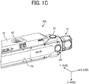
- FIG. 1C is an enlarged perspective view of the vicinity of a shutter button 62 of the image-capturing device 100.
- the image-capturing device 100 serves as a TOF distance measurement apparatus.
- the image-capturing device 100 includes a VCSEL projector unit 21, a TOF photosensor unit 61, a CMOS photosensor unit 30, a substrate (a CMOS substrate 35, VCSEL substrates 22F, 22B, and a main substrate 41), and a fan 38.
- the VCSEL projector unit 21 emits distance-measuring light (e.g., infrared light) toward an object to be measured to obtain a distance to the object.
- the VCSEL projector unit 21 includes two VCSEL projector units 21: VCSEL projector units 21F and 21B) (refer to FIG. 5 ), which will be described later in detail.
- the TOF photosensor unit 61 receives light scattered (scattering light) and reflected from the object to which the distance-measuring light has been emitted from the VCSEL projector unit 21, so as to obtain three-dimensional point group data.
- the CMOS photosensor unit 30 acquires a two-dimensional image using a CMOS sensor 33 (see FIG. 8 ).
- the substrates are substrates for driving or controlling the VCSEL projector unit 21, the TOF photosensor unit 61, and the CMOS photosensor unit 30.
- the substrates are connected to each of the VCSEL projector unit 21, the TOF photosensor unit 61, and the CMOS photosensor unit 30 via cables, flexible printed circuits (FPCs), and flexible flat cables (FFCs).
- the fan 38 is provided inside the image-capturing device 100 and generates forced convection to cool the inside of the image-capturing device 100.
- the following describes the arrangement of multiple substrates (the CMOS substrate 35, the VCSEL substrates 22F and 22B, and the main substrate 41) included in the image-capturing device 100.
- the CMOS substrate 35 is arranged between two VCSEL substrates 22F and 22B, which are aligned along the Z-axis.
- the main substrate 41 for controlling and driving the entire operations of the image-capturing device 100 is arranged in parallel with the three substrates.
- the main substrate 41 is disposed outside the VCSEL substrate 22B (i.e., on the -Z-side of the VCSEL substrate 22B, or closer to a rear cover 12 than the VCSEL substrate 22B.
- This configuration allows a total of four substrates (the VCSEL substrates 22F and 22B, the CMOS substrate 35, and the main substrate 41) to be housed within the image-capturing device 100 without wasting space inside the image-capturing device 100. This further enables downsizing of the four substrates (the VCSEL substrates 22F and 22B, the CMOS substrate 35, and the main substrate 41) in the arrangement direction of the substrates (i.e., along the Z-axis).
- the arrangement of the four substrates allows generation of air flows in the longitudinal direction of the substrates without hampering natural convective flows inside the image-capturing device 100 or forced convective flows by the fan 38, so as to reduce the occurrence of temperature deviations inside the image-capturing device 100. Further, since heat exhaust efficiency by inflow/outflow of air from a vent hole provided in a cover described later and heat radiation (heat transfer) from the cover to external air is improved, it is possible to reduce the occurrence of temperature rise inside the image-capturing device 100.
- the image-capturing device 100 includes battery cases 68a and 68b for housing batteries 18a and 18b (see FIG. 3 ), the shutter button 62, and an operation switch unit 17.
- the shutter button 62 allows a user operation to determine the image-capturing timing of the CMOS photosensor unit 30.
- the operation switch unit 17 allows a user operation to switch between ON and OFF of the image-capturing device 100 and switch an operation mode.
- the image-capturing device 100 includes covers (a front cover 11, a rear cover 12, a left cover 13, a right cover 14, battery covers 15a and 15b, a baseplate 16, and an inner wall 10 (see FIG. 2 ) for holding the above-described components.
- the image-capturing device 100 includes a screw hole 19 at the baseplate 16 (i.e., the -X-side of the image-capturing device 100) used to fix the image-capturing device 100 to, for example, a tripod to prevent the occurrence of hand shake during the shooting (the image-capturing operation).
- the image-capturing device 100 fixed to a tripod via the screw hole 19 provides more stable images than the image-capturing device 100 held by a user does.
- the image-capturing device 100 fixed to a tripod more effectively works to provide more stable images when remotely operated.
- FIG. 2 is an illustration of the inner wall 10 of the image-capturing device 100.
- the inner wall 10 connects the front cover 11 and the rear cover 12.
- a monocoque structure provided with a single cover (an single exterior component) according to a comparative example more likely have a lower stiffness
- the image-capturing device 100 according to the present embodiment is provided with the inner wall 10 connecting the front cover 11 and the rear cover 12 and has a higher stiffness.
- FIG. 3 is an illustration of battery cases 68a and 68b of the image-capturing device, according to an embodiment.
- the image-capturing device 100 includes built-in batteries 18a and 18b. With such an arrangement, the image-capturing device 100 allows a reduction in the burden of carrying and shooting work.
- the image-capturing device 100 includes a battery circuit board 67 provided with battery cases 68a and 68b, which is fixed to each side (i.e., each of the +Y side and the -Y side) of the inner wall 10.
- the battery cases 68a and 68b house the batteries 18a and 18b, respectively.
- Such a configuration facilitates replacement of the batteries 18a and 18b because in the image-capturing device 100, the batteries 18a and the 18b are attachable and detachable along the Y-axis by removing the battery covers 15a and 15b in FIG. 1A .
- the image-capturing device 100 may be driven by using a power cord.
- the power cord is preferably detachably attachable. Such a configuration eliminates the need for built-in batteries in the body of the image-capturing device 100 and thus achieves a reduction in the weight of the image-capturing device 100 while preventing longer image-capturing time.
- an insertion port of the power cord is preferably disposed at a lower portion closer to the baseplate 16 than the shutter button 62 (downstream of the shutter button 62 in the -X-direction). This arrangement allows light beams from being blocked by the fingers of the user pressing the shutter button 62 earlier than by the power code, and thus reduces the dead spot due to the power code more than the dead spot due to the fingers of the user.
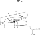
- FIG. 4 is a cross-sectional view of the shutter button 62.
- the image-capturing device 100 includes a switch 69 on the -Z-side of the main substrate 41. Further, the image-capturing device 100 includes the shutter button 62 on the rear cover 12, coaxially with the switch 69.
- This arrangement allows the direct pressing of the switch 69 using the shutter button 62 and thus achieves a reduction in the number of components and simplification of the structure. Further, directly pressing the switch 69 using the shutter button 62 further ensures a reliable reaction of the switch 69.
- the shutter button 62 and the switch 69 may be connected to each other via an intermediate member.
- the image-capturing device 100 includes a spring 63 between the main substrate 41 and the shutter button 62.
- the spring 63 serves to push back the shutter button 62 to a predetermined position when the user pushes and releases the shutter button 62.
- FIG. 5 is an illustration of the vicinity of the shutter button 62.
- the image-capturing device 100 includes a shutter button 62 in a region where a blind spot is generated by various covers (in the present embodiment, the rear cover 12).
- the angle of view (the lower side, or -X side) of the extreme periphery of the light beams emitted from the VCSEL projector unit 21F is ⁇ a.
- the angle of view ⁇ a is variable up to approximately 90 degrees.
- the light beams emitted from the VCSEL projector unit 21B present a shape in which a part of the rear cover 12 housing the main substrate 41 protrudes in the -Z-direction. With such a shape, the angle of view ⁇ b of the extreme periphery of the light beams emitted from the VCSEL projector unit 21 is greater than ⁇ b and less than ⁇ a ( ⁇ b ⁇ ⁇ a).
- This configuration prevents the extreme peripheral rays having the angle of view ⁇ b (i.e., light rays B emitted from the VCSEL projector unit 21B) from being at least partly blocked by the finger of the user when the shutter button 62 is in the vicinity of a place at the rear cover 12, indicated by arrow V as illustrated in FIG. 5 .
- the shutter button 62 is disposed on the opposite side (on the front cover 11)
- the rays having the angle of view ⁇ a (approximately 90 degrees) (i.e., light rays A emitted from the VCSEL projector unit 21F) is blocked by the finger of the user. This causes a reduction in the angle of view of the rays.
- the shutter button 62 is disposed between the TOF photosensor unit 61 and the batteries 18a and 18b. Such an arrangement of the shutter button 62 between the TOF photosensor unit 61 and the batteries 18a and 18b induces the user to hold the portion (a portion near the center of gravity) in which the batteries 18a and 18b are housed, and prevent camera shake while allowing a reduction in the user's fatigue.
- a remote operation may be performed in a wired or wireless manner. Such a remotely operable configuration prevents shake of the image-capturing device 100 held by the hand of the user more effectively.
- FIG. 6 is a cross-sectional view of the vicinity of the shutter button 62.
- the image-capturing device 100 includes multiple LED elements 65 (five LED elements in FIG. 6 ) on the -Z-side of the main substrate 41, so as to allow the LED elements 65 to indicate the operation state of the image-capturing device 100.
- the image-capturing device 100 includes openings 64 coaxial with the optical axes of the LED elements 65, respectively, on the rear cover 12. Such a configuration allows the image-capturing device 100 to emit the light beams emitted from the LED element 65 to the outside through the openings 64.
- the LED element 65 and the opening 64 may be connected by, for example, a light guide plate or an optical fiber. This arrangement increases the utilization efficiency of light in the image-capturing device 100.
- the image-capturing device 100 includes a lens system and a diffusion plate in the opening 64 to increase the viewability of images formed by light emitted from the LED element 65.
- FIG. 7A is a perspective view of a VCSEL projector unit 21.
- FIG. 7B is a cross-sectional view of a VCSEL optical system 23.
- FIG. 7C is an illustration of an arrangement example of the VCSEL projector unit 21.
- the VCSEL projector unit 21 includes a VCSEL substrate 22, a VCSEL package 24, and a lens cell 26.
- the VCSEL package 24 is a light source including a VCSEL as a light emitting point 25 (a light source).
- the lens cell 26 houses the VCSEL optical system 23 composed of multiple lenses.
- the VCSEL package 24 is soldered to each of the VCSEL substrates 22 (VCSEL substrates 22F and 22B).
- the VCSEL substrates 22F and 22B are collectively referred to as a VCSEL substrate 22.
- the VCSEL optical system 23 i.e., the lens cell 26
- the lens cell 26 is fixed to the VCSEL substrate 22 using a screw or bonded to the VCSEL substrate 22 so as to be aligned with the light emitting point 25 with a predetermined accuracy.
- the VCSEL substrate 22 (the VCSEL substrates 22F and 22B) is mounted with a drive circuit for driving the VCSEL package 24.
- the drive circuit of the VCSEL substrate 22 generates heat because a large current flows in order to increase the intensity of light emitted from the VCSEL package 24 serving as a light source.
- the VCSEL substrate 22 is mounted with a drive circuit having a large allowable current in order to reduce heat generation of the drive circuit, and is also mounted with a dissipator such as a heatsink.
- the VCSEL substrate 22 is larger than the other substrates, including the CMOS substrate 35. Such a configuration prevents the VCSEL substrate 22 from excessively heating up, and thus allows the VCSEL projector unit 21 to emit a higher intensity laser beam in the image-capturing device 100.
- the VCSEL projector unit 21 i.e., the VCSEL projector units 21F and 21B
- the VCSEL projector units 21F and 21B are arranged along the Z-axis to which the optical axes of the VCSEL optical systems 23 are parallel (or the optical axes of the VCSEL optical systems 23 of the VCSEL projector units 21F and 21B and the Z-axis are coincident with each other).
- the VCSEL projector units 21F and 21B face in opposite directions.
- the VCSEL optical system 23 serves as a fish-eye lens.
- the VCSEL optical systems 23 of the multiple phototransmitters 21 i.e., the VCSEL projector units 21F and 21B
- the range to be measured refers to a range actually irradiated with light beams emitted from the multiple phototransmitters: two VCSEL projector units 21F and 21B, within the full-spherical range of 4 ⁇ steradians with the image-capturing device 100 as the center.
- the range to be measured is equal to the full-spherical range of 4 ⁇ steradians measurement target range corresponds to the entire celestial sphere (full-spherical) (4 ⁇ steradians) in a situation where the light beams emitted from the VCSEL projector units 21F and 21B are not blocked by any of the components surrounding the VCSEL projector units 21F and 21B.
- the range to be measured is a range, within the full-spherical range, actually irradiated with light rays that have not been blocked by any of the components surrounding the phototransmitters 21.
- the VCSEL projector units 21F and 21B are fixed by fastening screws 66a (see FIG. 10 ) to the front cover 11 and the rear cover 12, respectively.
- positioning parts in the lens cells 26 of the VCSEL projector units 21F and 21B are positioned corresponding to positioning parts in the front cover 11 and the rear cover 12, respectively.
- This arrangement allows maintaining the accuracy of adjustment of the relative position (i.e., positioning) between the VCSEL projector unit 21F and the front cover 11 and the accuracy of adjustment of the relative position (i.e., positioning) between the VCSEL projector unit 21B and the rear cover 12.
- This configuration reduces or eliminates variations in the amount of light blocked by, for example, the front cover 11 and the rear cover 12 after emitted from the VCSEL projector units 21F and 21B, due to processing errors (dimension errors and shape errors) and also due to assembly variations of components of the image-capturing device 100. This reduction or elimination of variations in the amount of light blocked by any component further prevents poor illumination distribution of light emitted from the image-capturing device 100.
- the VCSEL substrates 22F and 22B are arranged in parallel to each other as illustrated in FIG. 10 described later.
- the VCSEL substrates 22F and 22B are to be larger in order to reduce overheating due to the emission of high intensity light from the VCSEL projector units 21F and 21B.
- the arrangement of the VCSEL substrates 22F and 22B of a large size in parallel allows downsizing of the image-capturing device 100 without interference between the VCSEL substrates 22F and 22B.
- the number of the VCSEL substrates 22F and 22B is minimum sufficient to project light to the full-spherical range to be measured, the downsizing of the image-capturing device 100 is achieved.
- FIG. 8 is a cross-sectional view of the CMOS photosensor unit 30.
- the CMOS photosensor unit 30 includes a CMOS optical system 31, a CMOS sensor substrate 32, and a lens holder 34.
- the CMOS optical system 31 includes multiple lenses, and a prism.
- the CMOS sensor 33 is mounted on the CMOS sensor substrate 32.
- the CMOS optical system 31 and the CMOS sensor substrate 32 are integrally held by the lens holder 34.
- the CMOS sensor substrate 32 is, for example, bonded to the holder 34a of the lens holder 34.
- the CMOS sensor 33 captures a luminance image or a red, green, and blue (RGB) image corresponding to the intensity of the scattering light reflected from the external object. Further, when light scattered and reflected from the object after the VCSEL projector unit 21 emits light to the object enters the CMOS optical system 31, the CMOS sensor 33 captures a luminance image with the wavelength of the light emitted from the VCSEL projector unit 21.
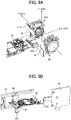
- FIG. 9A is an illustration of a CMOS substrate 35 connecting two CMOS photosensor units 30.
- FIG. 9B is an illustration of the arrangement of the CMOS substrate 35.
- the image-capturing device 100 is arranged with the optical axis of the CMOS optical systems 31 coincident with the Y-axis.
- two CMOS optical systems 31 as multiple imagers are disposed facing in the opposite directions (i.e., CMOS photosensor units 30R and 30L are disposed facing in the opposite directions).
- the CMOS sensor substrates 32 of the CMOS photosensor units 30R and 30L are connected to the common (one) CMOS substrate 35 by a cable such as a flexible printed circuit (FPC).
- FPC flexible printed circuit
- the CMOS substrate 35 is screwed via a spacer 37 onto a bracket 36L screwed to the left cover 13, a bracket 36R screwed to the right cover 14, and a bracket 36C screwed to the inner wall 10.
- the CMOS optical system 31 serves as a fish-eye lens.
- the CMOS optical systems 31 of the CMOS photosensor units 30R and 30L receive light beams scattered and reflected from the full-spherical range of 4 ⁇ steradians in a situation where light beams emitted from multiple photoemitters are not blocked by any of the surrounding components.
- FIG. 10 is an illustration of an arrangement example of a CMOS photosensor unit 30 and the VCSEL projector unit 21.
- CMOS photosensor unit 30 In the image-capturing device 100 as illustrated in FIGs. 1B and 10 , a part (or the entirety) of the CMOS photosensor unit 30 (or the lens holder 34) is disposed between two VCSEL substrates 22F and 22B. This arrangement allows downsizing of the image-capturing device 100 along the optical axis of the CMOS optical system 31 (i.e, the Y-axis).
- the CMOS photosensor units 30R and 30L are fixed to the right cover 14 and the left cover 13, using screws 66b, respectively.
- positioning parts in the lens cells 34 of the CMOS photosensor units 30R and 30L are positioned corresponding to positioning parts in the right cover 14 and the left cover 13, respectively.
- This arrangement allows maintaining the accuracy of adjustment of the relative position (i.e., positioning) between the CMOS photosensor unit 30R and the right cover 14 and the accuracy of adjustment of the relative position (i.e., positioning) between the CMOS photosensor unit 30L and the left cover 13.
- FIG. 11A is a perspective view of the external appearance of a TOF photosensor unit 61.
- FIG. 11B is a perspective view of the internal structure of the TOF photosensor unit 61.
- FIG. 11C is an illustration of the internal structure of the TOF photosensor unit 61, a part of which is cut away.
- the TOF photosensor unit 61 has a four-eye configuration.
- the TOF photosensor unit 61 includes TOF optical systems 71 (71A, 71B, 71C, 71D) as multiple photosensors that receive light reflected from a full-spherical range to be measured; TOF sensor substrates 74, a relay board 77, and a holder 78.
- Each TOF sensor substrate 74 is mounted with a TOF sensor 76.
- the relay board 77 serves as a relay between the TOF sensor substrates 74 and the main substrate 41.
- the TOF optical systems 71A, 71B, 71C, 71D and the TOF sensor substrates 74 are integrally held by the holder 78.
- the TOF sensor substrate 74 and the relay board 77 are connected by a cable such as an FPC, and the relay board 77 and the main substrate 41 are also connected by a cable such as an FPC.
- the TOF photosensor unit 61 having an integral structure enables simplification of an assembly/adjustment facility in a factory, reduction in an assembly/adjustment time, and quality assurance in the integral structure.
- the TOF photosensor unit 61 has an integrated structure, the image-capturing device 100 can be mounted on not only one model but also multiple models, and thus cost reduction can be achieved.
- FIGs. 12A and 12B are illustrations of the relative position between the TOF optical systems 71A, 71B, 71C, and 71D.
- the optical axis of the TOF optical system 71A is along the +X-direction (i.e., the TOF optical system 71B is disposed with its incidence plane facing in the +X-direction (upward in FIG. 12B ).
- the optical axes of the TOF optical systems 71B, 71C, and 71D are along the horizontal direction.
- the optical axis of the TOF optical system 71B is along the Y-axis (i.e., the TOF optical system 71B is disposed with its incidence plane facing the right (i.e., in the +Y-direction) in FIGs. 12A and 12B .
- At least one photosensor (71A) of the photosensors (71A to 71D) has an optical axis perpendicular to an optical axis of each of at least two photosensors (71B, 71C) of the photosensors (71A to 71D) excluding the at least one photosensor (71A).
- Each of the TOF optical systems 71C and 71D is arranged at an angle rotated by 120 degrees around the X-axis with respect to the TOF optical system 71B.
- the TOF optical system 71A vertically arranged has an angle of view (in the vertical direction; in an X-Y cross-sectional plane and an X-Z cross-sectional plane) of 65 degrees.
- the TOF optical system 71B horizontally arranged (with its incidence plane facing the right in FIGs. 12A and 12B ) has an angle of view of 85 degrees in the vertical direction (i.e., in the X-Y cross-sectional plane) and an angle of view of 65 degrees in the horizontal direction (in the Y-Z cross sectional plane).
- the same as described above for the TOF optical system 71B applies to the TOF optical systems 71C and 71D.
- Such an arrangement allows the TOF photosensor unit 61 of four-eye configuration in the image-capturing device 100 to receive light beams scattered and reflected from objects in all directions except for an area with an angle of view of 85 degrees or greater on the lower side of the Y-Z cross-sectional plane.
- the TOF optical system 71 (the TOF optical systems 71A, 71B, 71C, and 71D) has an angle of view smaller than the angle of view of the VCSEL optical system 23 (i.e., each of the photosensors has an angle of view smaller than a light-emitting range of each of the phototransmitters). With such a smaller angle of view, the TOF optical system 71 has a focal length longer than the focal length of the VCSEL optical system 23. Such a TOF optical system 71 receives a larger amount of light per unit angle of view, which is related to the amount of light per unit pixel received by the TOF sensor 76. This configuration allows an increase in the amount of light received by the TOF optical system 71, which has even been reflected from a distant object or a low-reflective object.
- FIG. 13 is a plan view of the VCSEL projector unit 21 and the TOF photosensor unit 61.
- FIG. 14 is an illustration of a relative position between the VCSEL optical system 23 and the TOF optical system 71, according to an embodiment of the present disclosure.
- FIG. 15 is an illustration of a relative position between a VCSEL optical system 23 and a TOF optical system 71, according to a comparative example. More specifically, FIG. 14 is an illustration of only the outermost lenses in the VCSEL projector unit 21 and the TOF photosensor unit 61, the lenses extracted from the plan view of the configuration of the image-capturing device 100 according to an embodiment in FIG. 13 .
- FIG. 15 indicates the configuration of the comparative example.
- the TOF optical systems 71B, 71C, and 71D are rotated about the X-axis by 30 degrees from the formation of the TOF optical systems 71B, 71C, and 71D in FIG. 14 .
- the VCSEL optical system 23F and the TOF optical system 71D are oriented in the same direction (+Z-direction).
- the image-capturing device of the arrangement in FIG. 15 causes the TOF optical system 71D to receive most of the light rays reflected from an object, which have been emitted to the object from the VCSEL optical system 23F on the +Z-side of the TOF optical system 71D.
- the TOF optical system 71B receives half of the amount of light scattered and reflected from an object after emitted from the VCSEL optical system 23B on the -Z-side of the TOF optical system 71D to the object, and the TOF optical system 71C receives the remainder of the amount of the light.
- the VCSEL optical systems 23F and 23B are disposed symmetrically with respect to the X-Y plane.
- the TOF optical systems 71B, 71C, and 71D are disposed symmetrically with respect to the X-Y plane.
- the phototransmitters each have an optical axis perpendicular to the optical axis of at least one photosensor (the TOF photosensor unit 71B) of the photosensors (the TOF photosensor units 71B, 71C, and 71D).
- the configuration in FIG. 15 the configuration in FIG.
- the image-capturing device 100 of the configuration in FIG. 14 achieves a much higher detection accuracy.
- FIG. 16 is an illustration of an angle of view of the VCSEL optical system 23.
- the image-capturing device 100 as illustrated in FIG. 16 includes the TOF optical system 71A of the TOF photosensor unit 61 in the first stage counted from the top (+X-side edge) and the TOF optical systems 71B, 71C, and 71D in the second stage.
- the image-capturing device 100 further includes the VCSEL optical systems 23F and 23B and the CMOS optical systems 31R and 31L in the third stage.
- the imagers each have an optical axis perpendicular to the optical axis of the at least one photosensor (the TOF optical system 71A) as illustrated in FIG. 16 .
- FIG. 16 schematically illustrates angles of view of the extreme peripheral light rays in a vertical cross section (Z-X cross-sectional plane) of the VCSEL optical system 23F and the TOF optical systems 71A and 71B.
- the TOF optical systems 71B, 71C, and 71D are rotated about the X-axis so that the optical axis of the TOF optical system 71B is parallel to the Z-axis.
- the TOF optical systems 71A to 71D and 171A to 171D are designed to have a wider angle of view (a maximum angle of view of 90 degrees) than the optical system illustrated in FIG. 12B .
- the VCSEL projector unit 21 covers a light-emitting range of a hemisphere (2 ⁇ steradians).
- the upper light-receivable range of the TOF photosensor unit 61 covers a hemispherical range: the light-receivable range of the TOF optical system 71A on the top of the TOF photosensor unit 61; and the light-receivable ranges (an angle of view ⁇ tof2) of the horizontally-arranged TOF optical systems 71B, 71C, and 71D.
- the image-capturing device 100 is capable of capturing an image of the entire image-capturing range of the upper hemisphere.
- the image-capturing range of the CMOS photosensor unit 30 refers to an overlapping area between the light-emitting range of the VCSEL projector unit 21 and the light-receivable range of the CMOS photosensor unit 30.
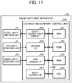
- FIG. 17 is a block diagram of the hardware configuration of the image-capturing device 100, according to an embodiment.
- the image-capturing device 100 includes a distance-measurement control unit 230 in addition to the VCSEL projector unit 21, the TOF photosensor unit 61, and the CMOS photosensor unit 30.
- the distance-measurement control unit 230 which is built in the cover, is connected to the VCSEL projector unit 21, the TOF photosensor unit 61, and the CMOS photosensor unit 30.
- the distance-measurement control unit 230 includes a central processing unit (CPU) 231, a read only memory (ROM) 232, a random access memory (RAM) 233, a solid state drive (SDD) 234, a light-source drive circuit 235, a sensor interface (I/F) 236, an input-output I/F 237, and an RGB sensor I/F 240. These components are electrically connected to each other via a system bus 242.
- the CPU 231 loads into the RAM 233 a program and data from a storage device, such as the ROM 232 or the SSD 234, and executes processing to provide the control or functions (described later) of the entirety of the distance-measurement control unit 230.
- a storage device such as the ROM 232 or the SSD 234.
- Some or the entirety of these functions of the CPU 231 may be implemented by electronic circuit such as an application specific integrated circuit (ASIC) and a field-programmable gate array (FPGA).
- ASIC application specific integrated circuit
- FPGA field-programmable gate array
- the ROM 232 is a non-volatile semiconductor memory (storage device) that holds a program and data although the power is turned off.
- the ROM 232 stores programs and data of, for example, a basic input/output system (BIOS) and an operating system (OS) that are executed when the image-capturing device 100 is activated.
- BIOS basic input/output system
- OS operating system
- the RAM 233 is a volatile semiconductor memory (storage device) that temporarily holds a program and data.
- the SSD 234 is a nonvolatile memory that stores programs for executing processing by the distance-measurement control unit 230 and various types of information. Note that the SSD may be a hard disk drive (HDD).
- HDD hard disk drive
- the light-source drive circuit 235 is an electric circuit that is electrically connected to the VCSEL projector unit 21 and outputs, to the VCSEL projector unit 21, a drive signal such as a drive voltage in response to a control signal input from the CPU 231. More specifically, in response to the control signal from the CPU 231, the light-source drive circuit 235 drives multiple light emitters included in the VCSEL projector unit 21 to emit light.
- the drive signal may use a rectangular wave, a sine wave, or a voltage waveform having a predetermined waveform.
- the light-source drive circuit 235 changes the frequency of the voltage waveform to modulate the frequency of the drive signal.
- the sensor I/F 236 is an interface that is electrically connected to the TOF photosensor unit 61 and receives a phase signal output from the TOF photosensor unit 61.
- the input-output I/F 237 is an interface for connecting with an external device such as a personal computer (PC).
- the RGB sensor I/F 240 is an interface that is electrically connected to the CMOS photosensor unit 30 and receives an RGB signal output from the CMOS photosensor unit 30.
- FIG. 18 is a block diagram of a functional configuration of the image-capturing device 100.
- the functional configuration of the image-capturing device 100 includes a distance-measurement control unit 230.
- the distance-measurement control unit 230 includes a light-emitting control unit 238, a light-receiving processing unit 239, and an RGB image processing unit 241.
- the distance-measurement control unit 230 controls the light emission of the VCSEL projector unit 21 via the light-emitting control unit 238, the light reception of the TOF photosensor unit 61 via the light-receiving processing unit 239, and the light reception of the CMOS photosensor unit 30 via the RGB image processing unit 241 in a synchronous manner.
- the light-emitting control unit 238 includes at least a drive-signal output unit 238a that implements a function of the image-capturing device 100.
- the drive-signal output unit 238a outputs a drive signal to the VCSEL projector units 21 and causes the VCSEL projector units 21 to simultaneously emit light beams. Further, the drive-signal output unit 238a outputs a drive signal having a predetermined voltage waveform at a predetermined light-emission frequency, thus to temporally modulate (temporally control) the light emission of the VCSEL projector units 21. In the present embodiment, the drive-signal output unit 238a outputs a drive signal having a rectangular wave or a sine wave at a frequency of about MHz to the VCSEL projector units 21 at a predetermined timing. This is only one example.
- the light-receiving processing unit 239 includes at least a phase-signal input unit 239a, a distance-image acquisition unit 239b, a storage unit 239c, and a distance-image combining unit 239d as functions of the image-capturing device 100.
- the phase-signal input unit 239a is implemented by the sensor I/F 236 to receive a phase signal output from the TOF photosensor unit 61.
- the phase-signal input unit 239a serves to receive a phase signal for each of the two-dimensionally arranged pixels in the TOF photosensor unit 61. Further, the phase-signal input unit 239a outputs the received phase signal to the distance-image acquisition unit 239b.
- the TOF photosensor unit 61 is connected to the phase-signal input unit 239a. In this case, the phase-signal input unit 239a outputs four phase signals for the TOF optical systems 71A, 71B, 71C, and 71D.
- the distance-image acquisition unit 239b acquires a distance-image data for the distance between the image-capturing device 100 and the object, based on the phase signal for each pixel from the TOF photosensor unit 61, input from the phase-signal input unit 239a.
- the distance image refers to an image in which pieces of distance data acquired on a pixel-by-pixel basis are two-dimensionally arranged at corresponding pixel positions.
- the distance image is an image generated with luminance data converted from the distance data.
- the distance-image acquisition unit 239b outputs the acquired four pieces of distance-image data to the storage unit 239c.
- the storage unit 239c is implemented by, for example, the RAM 233, and temporarily stores the distance image (four pieces of distance image data) received from the distance-image acquisition unit 239b.
- the distance-image combining unit 239d reads the four pieces of distance image data temporarily stored in the storage unit 239c, and combines the pieces of distance image data to generate one spherical distance image data.
- the distance-image combining unit 239d is implemented by the CPU 231 executing a control program. However, no limitation is intended thereby. In some embodiments, a part or the entirety of the distance-image combining unit 239d may be implemented by dedicated hardware designed to execute similar functions, for example, semiconductor integrated circuits such as an application specific integrated circuit (ASIC), a digital signal processor (DSP), and a field programmable gate array (FPGA), or typical circuit modules.
- ASIC application specific integrated circuit
- DSP digital signal processor
- FPGA field programmable gate array
- the RGB image processing unit 241 includes an RGB image input unit 241a, an RGB image storage unit 241b, and an RGB image combining unit 241c.
- the RGB image input unit 241a inputs an RGB image output from the CMOS photosensor unit 30.
- the RGB image input unit 241a serves to receive, from the CMOS photosensor unit 30, an RGB signal for each of the two-dimensionally arranged pixels in the CMOS photosensor unit 30.
- the RGB image input unit 241a outputs the received RGB image (signal) to the RGB image storage unit 241b (in the present embodiment, since the two CMOS photosensor units 30R and 30L are connected to the RGB image processing unit 241, two RGB images are output from the RGB image input unit 241a to the RGB image processing unit 241).
- the RGB image input unit 241a is implemented by the RGB sensor I/F 240, for example.
- the RGB image storage unit 241b is implemented by, for example, the RAM 233, and temporarily stores the RGB image input from the RGB image input unit 241a.
- the RGB image combining unit 241c reads two pieces of RGB image data temporarily stored in the RGB image storage unit 241b, and combines the two pieces of RGB image data to generate a single spherical RGB image (image data).
- the RGB image combining unit 241c is implemented when the CPU 231 executing a control program. However, no limitation is intended thereby. In some embodiments, a part or the entirety of the RGB image combining unit 241c may be implemented by dedicated hardware designed to execute similar functions, for example, semiconductor integrated circuits such as an ASIC, a DSP, and an FPGA, or typical circuit modules.
- the configuration in FIG. 18 is built in the image-capturing device 100, but the configuration is not limited to this example.
- the configuration in FIG. 18 may be included in an external information processing apparatus that is communicably connectable to the image-capturing device 100.
- the photosensors (the TOF optical systems 71A, 71B, 71C, and 71D) outnumber the phototransmitters (the VCSEL projector units 21F and 21B) to cover the range to be measured.
- This configuration allows upsizing of the light source of each phototransmitter to emit higher-intensity light. This enables reception of a sufficient amount of light even reflected from a distant object or a low-reflective object, and thus achieves a higher measurement accuracy.
- the photosensors outnumber the phototransmitters to cover the range to be measured, so as to allow each photosensor to have a smaller angle of view to receive light.
- each photosensor to have a longer focal length and a larger F-number lens, and thus achieves an increase in the accuracy of measurement of a distance to a distant object.
- the configuration according to an embodiment of the present disclosure uses photosensors more than phototransmitters and achieves higher intensities of light emitted from the phototransmitters, a longer focal length of the photosensors, and higher distance measurement accuracy with a limited size of the apparatus.
- the second embodiment differs from the first embodiment in that the TOF photosensor unit is divided into two upper and lower parts, and a VCSEL projector unit and a CMOS photosensor unit are disposed between the two parts.
- the description of the same portions as those of the first embodiment will be omitted, and portions different from those of the first embodiment will be described.
- the outermost lens of the VCSEL optical system 23F is disposed on the right (i.e., the +Z-side in FIG. 16 ) of the outermost lens of the TOF optical system 71B to allow the VCSEL optical system 23 to emit light with an upper light-emitting range of a hemisphere (2 ⁇ steradians).
- E1 is greater than D1 (E1 > D1) where E1 denotes a diameter of a circle passing through the points furthest from the X-axis, on the outermost lenses of the VCSEL optical systems 23F and 23B, respectively, and D1 denotes a diameter of a circle passing through the points furthest from the X-axis, on the outermost lenses of the TOF optical systems 71B, 71C, and 71D, respectively.
- the lower angle of view ⁇ tof3 of a light beam to be received by the TOF optical system 71B is set to prevent the light beam from being partly blocked by the VCSEL optical system 23F. Since the angle of view ⁇ tof3 is less than or equal to approximately 60 degrees ( ⁇ tof3 ⁇ 60 degrees), the dead spot A tends to be large. As a result, even when the angle of view ⁇ vcsel2 (the light-emitting range) on the lower side of the VCSEL optical system 23F is set to greater than 90 degrees ( ⁇ vcsel2 > 90 degrees), the image-capturing range is defined by the dead spot A on the lower side of the TOF optical system 71B. In such a case, the image-capturing device 100 fails to capture an image of the entire lower hemispherical range.
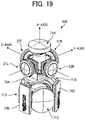
- FIG. 19 is an enlarged view of optical systems of an image-capturing device 200 according to the second embodiment.
- the TOF photosensor unit is divided into two upper and lower parts, and VCSEL projector units (VCSEL optical systems 23F and 23B) and CMOS photosensor units (CMOS optical systems 31R and 31L) are disposed between the two parts. More specifically, in the image-capturing device 200, the TOF optical system 71A is disposed in the first stage, the TOF optical systems 71B, 71C, and 71D are disposed in the third stage, and the VCSEL optical systems 23F and 23B and the CMOS optical systems 31R and 31L are disposed in the second state between the first state and the third stage.
- the phototransmitters are between the at least one photosensor (the TOF optical system 71A) and the at least two photosensors (the TOF optical systems 71B and 71C) of the photosensors (71A to 71D) excluding the at least one photosensors (the TOF optical system 71A).
- FIG. 20 is an illustration of an angle of view of a VCSEL optical system 123.
- FIG. 20 schematically illustrates light rays at the extreme peripheral angle of view in a vertical cross section (Z-X cross-sectional plane) of the VCSEL optical system 23F and the TOF optical systems 71A and 71B.
- at least one photosensor (the TOF optical system 71A) of the photosensors (the TOF optical systems 71A to 71D) has an optical axis perpendicular to an optical axis of each of at least two photosensors (the TOF optical systems 71B, 71C) of the photosensors (71A to 71D) excluding the at least one photosensor (the TOF optical system 71A).
- the photosensors (the TOF optical systems 71A to 71D) outnumber the imagers (the CMOS optical systems 31R and 31L).
- the imagers (the CMOS optical systems 31R and 31L) are between the at least one photosensor (the TOF optical system 71A) and the at least two photosensors (the TOF optical systems 71B and 71C) of the photosensors (71A to 71D) excluding the at least one photosensors (the TOF optical system 71A).
- the TOF optical systems 71B, 71C, and 71D are rotated about the X-axis so that the optical axis of the TOF optical system 71B is parallel to the Z-axis.
- the upper light-emitting range of the VCSEL projector unit (the VCSEL optical systems 23F and 23B) is increased to have an extreme peripheral angle of view ⁇ vcsel2 of greater than 90 degrees, so as to cover a hemispherical range of 2 ⁇ steradians.
- the image-capturing device 200 allows the TOF photosensor unit as a whole to cover the upper light-receivable range of a hemispherical range of 2 ⁇ steradians, which is a combination of the upper light-receivable range with an angle of view ⁇ vcsel2 of each of the TOF optical systems 71B, 71C, and 71D and the light-receivable range of an angle of view Qvcsell of the TOF optical system 71A.
- the image-capturing device 200 is capable of capturing an image of the entire image-capturing range of the upper hemisphere.
- the TOF optical system 71A is disposed on the upper side of the VCSEL optical system 23F in the second stage.
- E2 denotes a diameter of a circle passing through the points furthest from the X-axis on the outermost lenses of the VCSEL optical systems 23F and 23B
- D2 denotes a diameter of a circle passing through the points furthest from the X-axis on the outermost lenses of the TOF optical systems 71B, 71C, and 71D.
- the configuration according to the present embodiment eliminates the need for increasing the size along the Z-axis and thus achieves downsizing of the image-capturing device 100.
- the lower angle of view Qtof2 of the extreme peripheral rays emitted from the VCSEL optical system 23F may be increased to a degree ( ⁇ vcsel2 ⁇ approximately 85 degrees) that prevents a light beam emitted from the VCSEL optical system 23F from being at least partly blocked by the TOF optical system 71B.
- the image-capturing device 200 allows a light-receivable range of the TOF photosensor unit to have an angle of view of 90 degrees at the maximum in the Z-X cross-sectional plane because of the lower light-receivable range (of the angle of view Qtof3) of the TOF optical system 71B.
- the image-capturing device 200 is capable of capturing an image of the entire image-capturing range of the lower hemisphere by incorporating the light-receivable ranges of the TOF optical systems 71C and 71D.
- the present embodiment allows capturing of an image over the entire image-capturing range.
- the range to be measured (or the image-capturing range) is a full-spherical range to which the phototransmitters (23F, 23B) emit the light beams.
- the distance measurement apparatus (the image-capturing devices 100, 200) includes VCSEL projector units 21F and 21B as multiple phototransmitters, TOF optical systems 71 (71A, 71B, 71C, 71D) as multiple photosensors, CMOS photosensor units 30R and 30L as multiple imagers, and a distance-measurement control unit 230 that performs distance-measurement calculation, which are formed as a single integrated unit.
- the distance-measurement apparatus is not limited to such a single integrated unit.
- a distance-measurement system 100' is configured by connecting the following devices to each other via a network: a projector unit 21' (a projector) including VCSEL projector units 21F and 21B as multiple phototransmitters, a TOF photosensor unit 71' (photosensor unit, photosensor device) including TOF optical systems 71 (71A, 71B, 71C, 71D) as multiple photosensors, a CMOS imaging unit 30' (an imager unit) including CMOS photosensor units 30R and 30L as multiple imagers, and a distance-measurement control unit 250 including a CPU and a memory to perform distance-measurement calculation.
- a projector unit 21' a projector
- VCSEL projector units 21F and 21B multiple phototransmitters
- TOF photosensor unit 71' photosensor unit, photosensor device
- TOF optical systems 71 71A, 71B, 71C, 71D
- CMOS imaging unit 30' an imager unit
- a distance measurement apparatus (100, 200) includes: multiple phototransmitters (21F, 21B) configured to emit light beams to a range to be measured; multiple photosensors (71A to 71D) each configured to receive a light beam reflected from an object within the range to be measured; and a distance-measurement control unit (230) configured to calculate a distance to the object based on time of light emission of each of the phototransmitters (21F, 21B) and time of light reception of each of the photosensors (71A to 71D).
- the photosensors outnumber the phototransmitters (21F, 21B).
- each of the photosensors (71A to 71D) has an angle of view smaller than a light-emitting range of each of the phototransmitters (21F, 21B).
- At least one photosensor (71A) of the photosensors (71A to 71D) has an optical axis perpendicular to an optical axis of each of at least two photosensors (71B, 71C) of the photosensors (71A to 71D) excluding the at least one photosensor (71A).
- the phototransmitters (23F, 23B) each have an optical axis perpendicular to the optical axis of the at least one photosensor (71A).
- the distance measurement apparatus (100, 200) according to any one of Aspects 1 to 3, further includes multiple imagers (30R, 30L) each configured to capture an image of a view within the range to be measured.
- the distance measurement apparatus (100, 200) further includes multiple imagers (31R, 31L) each configured to capture an image of a view within the range to be measured.
- the photosensors (71A to 71D) outnumber the imagers (31R, 31L).
- the imagers (31R, 31L) each have an optical axis perpendicular to the optical axis of the at least one photosensor (71A).
- At least one photosensor (71A) of the photosensors (71A to 71D) has an optical axis perpendicular to an optical axis of each of at least two photosensors (71B, 71C) of the photosensors (71A to 71D) excluding the at least one photosensor (71A).
- the phototransmitters (23F, 23B) are between the at least one photosensor (71A) and the at least two photosensors (71B, 71C).
- the distance measurement apparatus (100, 200) according to Aspect 6, further includes multiple imagers (31R, 31L) each configured to capture images of views within the range to be measured.
- the photosensors (71A to 71D) outnumber the imagers (31R, 31L).
- the imagers (31R, 31L) are between the at least one photosensor (71A) and the at least two photosensors (71B, 71C).
- each of the photosensors (71A to 71D) receives light beams from at least two of the phototransmitters (21F, 21B).
- the range to be measured is a full-spherical range.
- a distance measurement system (100') includes a projector unit (21') including multiple phototransmitters (21F, 21B) configured to emit light beams to a range to be measured; a photosensor unit (71') including multiple photosensors (71A to 71D) each configured to receive a light beam reflected from an object within the range to be measured; and a distance-measurement control unit (250) configured to calculate a distance to the object based on time of light emission of each of the phototransmitters (21F, 21B) and time of light reception of each of the photosensors (71A to 71D).
- the photosensors (71A to 71D) outnumber the phototransmitters (21F, 21B).
- the distance measurement system (100') further includes an imager unit (30') including multiple imagers (30L, 30R) each configured to capture an image of a view of the range to be measured.
- the present invention can be implemented in any convenient form, for example using dedicated hardware, or a mixture of dedicated hardware and software.
- the present invention may be implemented as computer software implemented by one or more networked processing apparatuses.
- the processing apparatuses include any suitably programmed apparatuses such as a general purpose computer, a personal digital assistant, a Wireless Application Protocol (WAP) or third-generation (3G)-compliant mobile telephone, and so on. Since the present invention can be implemented as software, each and every aspect of the present invention thus encompasses computer software implementable on a programmable device.
- the computer software can be provided to the programmable device using any conventional carrier medium (carrier means).
- the carrier medium includes a transient carrier medium such as an electrical, optical, microwave, acoustic or radio frequency signal carrying the computer code.
- transient medium is a Transmission Control Protocol/Internet Protocol (TCP/IP) signal carrying computer code over an IP network, such as the Internet.
- the carrier medium may also include a storage medium for storing processor readable code such as a floppy disk, a hard disk, a compact disc read-only memory (CD-ROM), a magnetic tape device, or a solid state memory device.
Landscapes
- Engineering & Computer Science (AREA)
- Physics & Mathematics (AREA)
- Radar, Positioning & Navigation (AREA)
- Remote Sensing (AREA)
- Computer Networks & Wireless Communication (AREA)
- General Physics & Mathematics (AREA)
- Electromagnetism (AREA)
- Optical Radar Systems And Details Thereof (AREA)
- Length Measuring Devices By Optical Means (AREA)
- Measurement Of Optical Distance (AREA)
Abstract
A distance measurement apparatus (100) including: multiple phototransmitters to emit light beams to a range to be measured, preferably from VCSEL optical systems (23F, 23B); multiple photosensors (71A to 71D) each to receive a light beam reflected from an object within the range to be measured; and a distance-measurement control unit to calculate a distance to the object based on time of light emission of each of the phototransmitters and time of light reception of each of the photosensors. The photosensors (71A to 71D) outnumber the phototransmitters. A TOF photosensor unit (61) includes the TOF optical systems (71A, 71B, 71C, 71D) as multiple photosensors that receive light reflected from a full-spherical range to be measured so as to obtain three-dimensional point group data. The TOF optical system (71A) of the TOF photosensor unit (61) is in a first stage and the TOF optical systems (71B, 71C, and 71D) are in a second stage. The VCSEL optical systems (23F, 23B) and CMOS optical systems (31R, 31L) of a CMOS photosensor unit are in a third stage. The CMOS photosensor unit acquires a two-dimensional image. The VCSEL optical system (23B, 23F) serves as a fish-eye lens and emits emits light beam to a full-spherical range to be measured with the emitted light beams.
Description
- The present disclosure relates to a distance measurement apparatus and a distance measurement system.
- As an example of ranging (or distance measurement), the time-of-flight (TOF) is known that includes emitting light for ranging toward an object and obtaining a time difference between the emitting time and the time of receiving light reflected from the object to calculate a distance to the object using the time difference. In the TOF, the image sensor for infrared light receives light for ranging reflected from an object after the light having an intensity modulated according to a predetermined irradiation pattern is emitted to the object. A time difference between the light emitting time and the light receiving time for the irradiation pattern is detected for each pixel to calculate a distance to the object. The calculated distance values are collected in a bitmap form for the respective pixels, which are stored as a distance image. Such a distance image generation apparatus (a distance measurement apparatus) is referred to as a TOF camera.
- For example,
Japanese Unexamined Patent Application Publication No. 2019-159284 - However, the technology of
Japanese Unexamined Patent Application Publication No. 2019-159284 - In view of the above, an object of the present disclosure is to achieve a higher distance measurement accuracy with a limited size of the apparatus.
- An embodiment provides a distance measurement apparatus (100, 200) including: multiple phototransmitters (21F, 21B) configured to emit light beams to a range to be measured; multiple photosensors (71A to 71D) each configured to receive a light beam reflected from an object within the range to be measured; and a distance-measurement control unit (230) configured to calculate a distance to the object based on time of light emission of each of the phototransmitters (21F, 21B) and time of light reception of each of the photosensors (71A to 71D). The photosensors (71A to 71D) outnumber the phototransmitters (21F, 21B).
- Another embodiment provides a distance measurement system including a projector including multiple phototransmitters (21F, 21B) configured to emit light beams to a range to be measured; a photosensor device including multiple photosensors (71A to 71D) each configured to receive a light beam reflected from an object within the range to be measured; and circuitry configured to calculate a distance to the object based on time of light emission of each of the phototransmitters (21F, 21B) and time of light reception of each of the photosensors (71A to 71D). The photosensors (71A to 71D) outnumber the phototransmitters (21F, 21B).
- Embodiments of the present disclosure use photosensors more than phototransmitters to achieve higher intensities of light emitted from the phototransmitters, longer focal length of photosensors, and higher distance measurement accuracy within a limited size of the apparatus.
- A more complete appreciation of the disclosure and many of the attendant advantages and features thereof can be readily obtained and understood from the following detailed description with reference to the accompanying drawings, wherein:
-
FIG. 1A is an external perspective view of an image-capturing device according to a first embodiment; -
FIG. 1B is a perspective view of the internal configuration of the image-capturing device inFIG. 1A ; -
FIG. 1C is an enlarged perspective view of the vicinity of a shutter button of the image-capturing device; -
FIG. 2 is an illustration of the inner wall of the image-capturing device, according to an embodiment; -
FIG. 3 is an illustration of a battery case of the image-capturing device, according to an embodiment; -
FIG. 4 is a cross-sectional view of the shutter button inFIG. 1C ; -
FIG. 5 is another illustration of the vicinity of the shutter button; -
FIG. 6 is another cross-sectional view of the vicinity of the shutter button; -
FIG. 7A is a perspective view of a vertical-cavity surface-emitting lasers (VCSEL) projector unit; -
FIG. 7B is a cross-sectional view of a VCSEL optical system; -
FIG. 7C is an illustration of an arrangement example of the VCSEL projector units; -
FIG. 8 is a cross-sectional view of a complementary metal oxide semiconductor (CMOS) photosensor unit; -
FIG. 9A is an illustration of how two CMOS photosensor units are connected by a CMOS substrate; -
FIG. 9B is an illustration of an arrangement of the CMOS substrate illustrating an arrangement of a CMOS substrate. -
FIG. 10 is an illustration of an arrangement example of a CMOS photosensor unit and the VCSEL projector unit; -
FIG. 11A is an external perspective view of a TOF photosensor unit; -
FIG. 11B is a perspective view of the internal configuration of the TOF photosensor unit; -
FIG. 11C is an illustration of a part of the internal configuration of the TOF photosensor unit; -
FIG. 12A is an illustration of a relative position between TOF optical systems; -
FIG. 12B is another illustration of a relative position between TOF optical systems; -
FIG. 13 is a plan view of the VCSEL projector unit and the TOF photosensor unit; -
FIG. 14 is an illustration of a relative position between VCSEL optical systems and the TOF optical systems, according to an embodiment of the present disclosure; -
FIG. 15 is an illustration of a relative position between VCSEL optical systems and the TOF optical systems, according to a comparative example; -
FIG. 16 is an illustration of an angle of view of the VCSEL optical system; -
FIG. 17 is a block diagram of the hardware configuration of the image-capturing device, according to an embodiment; -
FIG. 18 is a block diagram of the functional configuration of the image-capturing device; -
FIG. 19 is an enlarged view of optical systems of an image-capturingdevice 200 according to a second embodiment; -
FIG. 20 is an illustration of an angle of view of the VCSEL optical system; and -
FIG. 21 is a block diagram of a hardware configuration of a distance measurement system according to an embodiment. - The accompanying drawings are intended to depict embodiments of the present invention and should not be interpreted to limit the scope thereof. The accompanying drawings are not to be considered as drawn to scale unless explicitly noted. Also, identical or similar reference numerals designate identical or similar components throughout the several views.
- In describing embodiments illustrated in the drawings, specific terminology is employed for the sake of clarity. However, the disclosure of this specification is not intended to be limited to the specific terminology so selected and it is to be understood that each specific element includes all technical equivalents that have a similar function, operate in a similar manner, and achieve a similar result.
- Referring now to the drawings, embodiments of the present disclosure are described below. As used herein, the singular forms "a," "an," and "the" are intended to include the plural forms as well, unless the context clearly indicates otherwise.
- Hereinafter, embodiments of a distance measurement apparatus and a distance measurement system will be described in detail with reference to the accompanying drawings.
-
FIG. 1A is an external perspective view of the configuration of an image-capturingdevice 100 according to a first embodiment.FIG. 1B is a perspective view of the internal configuration of the image-capturingdevice 100.FIG. 1C is an enlarged perspective view of the vicinity of ashutter button 62 of the image-capturingdevice 100. The image-capturingdevice 100 serves as a TOF distance measurement apparatus. - As illustrated in
FIGs. 1A to 1C , the image-capturingdevice 100 includes aVCSEL projector unit 21, aTOF photosensor unit 61, aCMOS photosensor unit 30, a substrate (aCMOS substrate 35,VCSEL substrates fan 38. - The
VCSEL projector unit 21 emits distance-measuring light (e.g., infrared light) toward an object to be measured to obtain a distance to the object. TheVCSEL projector unit 21 includes two VCSEL projector units 21:VCSEL projector units FIG. 5 ), which will be described later in detail. - The
TOF photosensor unit 61 receives light scattered (scattering light) and reflected from the object to which the distance-measuring light has been emitted from theVCSEL projector unit 21, so as to obtain three-dimensional point group data. - The
CMOS photosensor unit 30 acquires a two-dimensional image using a CMOS sensor 33 (seeFIG. 8 ). - The substrates (the
CMOS substrate 35, theVCSEL substrates VCSEL projector unit 21, theTOF photosensor unit 61, and theCMOS photosensor unit 30. The substrates (theCMOS substrate 35, theVCSEL substrates VCSEL projector unit 21, theTOF photosensor unit 61, and theCMOS photosensor unit 30 via cables, flexible printed circuits (FPCs), and flexible flat cables (FFCs). - The
fan 38 is provided inside the image-capturingdevice 100 and generates forced convection to cool the inside of the image-capturingdevice 100. - The following describes the arrangement of multiple substrates (the
CMOS substrate 35, theVCSEL substrates device 100. - As illustrated in
FIG. 1B , theCMOS substrate 35 is arranged between twoVCSEL substrates main substrate 41 for controlling and driving the entire operations of the image-capturingdevice 100 is arranged in parallel with the three substrates. Themain substrate 41 is disposed outside theVCSEL substrate 22B (i.e., on the -Z-side of theVCSEL substrate 22B, or closer to arear cover 12 than theVCSEL substrate 22B. - This configuration allows a total of four substrates (the
VCSEL substrates CMOS substrate 35, and the main substrate 41) to be housed within the image-capturingdevice 100 without wasting space inside the image-capturingdevice 100. This further enables downsizing of the four substrates (theVCSEL substrates CMOS substrate 35, and the main substrate 41) in the arrangement direction of the substrates (i.e., along the Z-axis). Further, the arrangement of the four substrates (i.e, theVCSEL substrates CMOS substrate 35, and themain substrate 41 are arranged in parallel to each other) allows generation of air flows in the longitudinal direction of the substrates without hampering natural convective flows inside the image-capturingdevice 100 or forced convective flows by thefan 38, so as to reduce the occurrence of temperature deviations inside the image-capturingdevice 100. Further, since heat exhaust efficiency by inflow/outflow of air from a vent hole provided in a cover described later and heat radiation (heat transfer) from the cover to external air is improved, it is possible to reduce the occurrence of temperature rise inside the image-capturingdevice 100. - As illustrated in
FIG. 1A to 1C , the image-capturingdevice 100 includesbattery cases housing batteries FIG. 3 ), theshutter button 62, and anoperation switch unit 17. - The
shutter button 62 allows a user operation to determine the image-capturing timing of theCMOS photosensor unit 30. - The
operation switch unit 17 allows a user operation to switch between ON and OFF of the image-capturingdevice 100 and switch an operation mode. - Further, as illustrated in
FIGs. 1A to 1C , the image-capturingdevice 100 includes covers (afront cover 11, arear cover 12, aleft cover 13, aright cover 14, battery covers 15a and 15b, abaseplate 16, and an inner wall 10 (seeFIG. 2 ) for holding the above-described components. - As illustrated in
FIG. 1A , the image-capturingdevice 100 includes ascrew hole 19 at the baseplate 16 (i.e., the -X-side of the image-capturing device 100) used to fix the image-capturingdevice 100 to, for example, a tripod to prevent the occurrence of hand shake during the shooting (the image-capturing operation). The image-capturingdevice 100 fixed to a tripod via thescrew hole 19 provides more stable images than the image-capturingdevice 100 held by a user does. The image-capturingdevice 100 fixed to a tripod more effectively works to provide more stable images when remotely operated. - The
inner wall 10 that is a part of the covers of the image-capturingdevice 100 is described below.FIG. 2 is an illustration of theinner wall 10 of the image-capturingdevice 100. - As illustrated in
FIG. 2 , theinner wall 10 connects thefront cover 11 and therear cover 12. Although a monocoque structure provided with a single cover (an single exterior component) according to a comparative example more likely have a lower stiffness, the image-capturingdevice 100 according to the present embodiment is provided with theinner wall 10 connecting thefront cover 11 and therear cover 12 and has a higher stiffness. - Next, the
battery cases FIG. 3 is an illustration ofbattery cases - As illustrated in
FIG. 3 , the image-capturingdevice 100 includes built-inbatteries device 100 allows a reduction in the burden of carrying and shooting work. The image-capturingdevice 100 includes abattery circuit board 67 provided withbattery cases inner wall 10. Thebattery cases batteries - Such a configuration facilitates replacement of the
batteries device 100, thebatteries 18a and the 18b are attachable and detachable along the Y-axis by removing the battery covers 15a and 15b inFIG. 1A . - The image-capturing
device 100 may be driven by using a power cord. The power cord is preferably detachably attachable. Such a configuration eliminates the need for built-in batteries in the body of the image-capturingdevice 100 and thus achieves a reduction in the weight of the image-capturingdevice 100 while preventing longer image-capturing time. - In such a configuration using a power code to drive the image-capturing
device 100, an insertion port of the power cord is preferably disposed at a lower portion closer to thebaseplate 16 than the shutter button 62 (downstream of theshutter button 62 in the -X-direction). This arrangement allows light beams from being blocked by the fingers of the user pressing theshutter button 62 earlier than by the power code, and thus reduces the dead spot due to the power code more than the dead spot due to the fingers of the user. - The following describes the
shutter button 62.FIG. 4 is a cross-sectional view of theshutter button 62. - As illustrated in
FIG. 4 , the image-capturingdevice 100 includes aswitch 69 on the -Z-side of themain substrate 41. Further, the image-capturingdevice 100 includes theshutter button 62 on therear cover 12, coaxially with theswitch 69. This arrangement allows the direct pressing of theswitch 69 using theshutter button 62 and thus achieves a reduction in the number of components and simplification of the structure. Further, directly pressing theswitch 69 using theshutter button 62 further ensures a reliable reaction of theswitch 69. In some embodiments in which theshutter button 62 and theswitch 69 are separated from each other, theshutter button 62 and theswitch 69 may be connected to each other via an intermediate member. - As illustrated in
FIG. 4 , the image-capturingdevice 100 includes aspring 63 between themain substrate 41 and theshutter button 62. Thespring 63 serves to push back theshutter button 62 to a predetermined position when the user pushes and releases theshutter button 62. - Next, the arrangement of the
shutter button 62 will be described.FIG. 5 is an illustration of the vicinity of theshutter button 62. - As illustrated in
FIG. 5 , the image-capturingdevice 100 includes ashutter button 62 in a region where a blind spot is generated by various covers (in the present embodiment, the rear cover 12). - Specifically, in the X-Z cross-sectional plane in
FIG. 5 , the angle of view (the lower side, or -X side) of the extreme periphery of the light beams emitted from theVCSEL projector unit 21F is θa. The angle of view θa is variable up to approximately 90 degrees. The light beams emitted from theVCSEL projector unit 21B present a shape in which a part of therear cover 12 housing themain substrate 41 protrudes in the -Z-direction. With such a shape, the angle of view θb of the extreme periphery of the light beams emitted from theVCSEL projector unit 21 is greater than θb and less than θa (θb < θa). This configuration prevents the extreme peripheral rays having the angle of view θb (i.e., light rays B emitted from theVCSEL projector unit 21B) from being at least partly blocked by the finger of the user when theshutter button 62 is in the vicinity of a place at therear cover 12, indicated by arrow V as illustrated inFIG. 5 . However, when theshutter button 62 is disposed on the opposite side (on the front cover 11), the rays having the angle of view θa (approximately 90 degrees) (i.e., light rays A emitted from theVCSEL projector unit 21F) is blocked by the finger of the user. This causes a reduction in the angle of view of the rays. - The
shutter button 62 is disposed between theTOF photosensor unit 61 and thebatteries shutter button 62 between theTOF photosensor unit 61 and thebatteries batteries - Instead of determining the shooting timing by pressing and releasing the
shutter button 62 on therear cover 12 of the image-capturingdevice 100, a remote operation may be performed in a wired or wireless manner. Such a remotely operable configuration prevents shake of the image-capturingdevice 100 held by the hand of the user more effectively. -
FIG. 6 is a cross-sectional view of the vicinity of theshutter button 62. As illustrated inFIG. 6 , the image-capturingdevice 100 includes multiple LED elements 65 (five LED elements inFIG. 6 ) on the -Z-side of themain substrate 41, so as to allow theLED elements 65 to indicate the operation state of the image-capturingdevice 100. Further, the image-capturingdevice 100 includesopenings 64 coaxial with the optical axes of theLED elements 65, respectively, on therear cover 12. Such a configuration allows the image-capturingdevice 100 to emit the light beams emitted from theLED element 65 to the outside through theopenings 64. - In the image-capturing
device 100, theLED element 65 and theopening 64 may be connected by, for example, a light guide plate or an optical fiber. This arrangement increases the utilization efficiency of light in the image-capturingdevice 100. In some embodiments, the image-capturingdevice 100 includes a lens system and a diffusion plate in theopening 64 to increase the viewability of images formed by light emitted from theLED element 65. - Next, the
VCSEL projector unit 21 will be described.FIG. 7A is a perspective view of aVCSEL projector unit 21.FIG. 7B is a cross-sectional view of a VCSELoptical system 23.FIG. 7C is an illustration of an arrangement example of theVCSEL projector unit 21. - As illustrated in
FIGs. 7A to 7C , theVCSEL projector unit 21 includes aVCSEL substrate 22, aVCSEL package 24, and alens cell 26. - The
VCSEL package 24 is a light source including a VCSEL as a light emitting point 25 (a light source). Thelens cell 26 houses the VCSELoptical system 23 composed of multiple lenses. - The
VCSEL package 24 is soldered to each of the VCSEL substrates 22 (VCSEL substrates VCSEL substrates VCSEL substrates VCSEL substrate 22. Further, the VCSEL optical system 23 (i.e., the lens cell 26) is fixed to theVCSEL substrate 22 using a screw or bonded to theVCSEL substrate 22 so as to be aligned with thelight emitting point 25 with a predetermined accuracy. - The VCSEL substrate 22 (the
VCSEL substrates VCSEL package 24. The drive circuit of theVCSEL substrate 22 generates heat because a large current flows in order to increase the intensity of light emitted from theVCSEL package 24 serving as a light source. To handle such generated heat, theVCSEL substrate 22 is mounted with a drive circuit having a large allowable current in order to reduce heat generation of the drive circuit, and is also mounted with a dissipator such as a heatsink. To mount such components on theVCSEL substrate 22, theVCSEL substrate 22 is larger than the other substrates, including theCMOS substrate 35. Such a configuration prevents theVCSEL substrate 22 from excessively heating up, and thus allows theVCSEL projector unit 21 to emit a higher intensity laser beam in the image-capturingdevice 100. - As illustrated in
FIG. 7C , the VCSEL projector unit 21 (i.e., theVCSEL projector units optical systems 23 are parallel (or the optical axes of the VCSELoptical systems 23 of theVCSEL projector units VCSEL projector units - The VCSEL
optical system 23 serves as a fish-eye lens. The VCSELoptical systems 23 of the multiple phototransmitters 21 (i.e., theVCSEL projector units VCSEL projector units - The range to be measured refers to a range actually irradiated with light beams emitted from the multiple phototransmitters: two
VCSEL projector units device 100 as the center. As described above, the range to be measured is equal to the full-spherical range of 4π steradians measurement target range corresponds to the entire celestial sphere (full-spherical) (4π steradians) in a situation where the light beams emitted from theVCSEL projector units VCSEL projector units VCSEL projector units phototransmitters 21. - In the image-capturing
device 100, theVCSEL projector units fastening screws 66a (seeFIG. 10 ) to thefront cover 11 and therear cover 12, respectively. In this case, positioning parts in thelens cells 26 of theVCSEL projector units front cover 11 and therear cover 12, respectively. This arrangement allows maintaining the accuracy of adjustment of the relative position (i.e., positioning) between theVCSEL projector unit 21F and thefront cover 11 and the accuracy of adjustment of the relative position (i.e., positioning) between theVCSEL projector unit 21B and therear cover 12. - This configuration reduces or eliminates variations in the amount of light blocked by, for example, the
front cover 11 and therear cover 12 after emitted from theVCSEL projector units device 100. This reduction or elimination of variations in the amount of light blocked by any component further prevents poor illumination distribution of light emitted from the image-capturingdevice 100. - The
VCSEL substrates FIG. 10 described later. TheVCSEL substrates VCSEL projector units VCSEL substrates device 100 without interference between theVCSEL substrates VCSEL substrates device 100 is achieved. - Next, the
CMOS photosensor unit 30 will be described.FIG. 8 is a cross-sectional view of theCMOS photosensor unit 30. - As illustrated in
FIG. 8 , theCMOS photosensor unit 30 includes a CMOSoptical system 31, aCMOS sensor substrate 32, and alens holder 34. - The CMOS
optical system 31 includes multiple lenses, and a prism. TheCMOS sensor 33 is mounted on theCMOS sensor substrate 32. The CMOSoptical system 31 and theCMOS sensor substrate 32 are integrally held by thelens holder 34. TheCMOS sensor substrate 32 is, for example, bonded to theholder 34a of thelens holder 34. - In the image-capturing
device 100, scattering light reflected from an external object, which has been emitted from an external illumination or theVCSEL projector unit 21, enters the CMOSoptical system 31 and reaches theCMOS sensor 33 as indicated by arrow S inFIG. 8 . When the external illumination is a white light source, theCMOS sensor 33 captures a luminance image or a red, green, and blue (RGB) image corresponding to the intensity of the scattering light reflected from the external object. Further, when light scattered and reflected from the object after theVCSEL projector unit 21 emits light to the object enters the CMOSoptical system 31, theCMOS sensor 33 captures a luminance image with the wavelength of the light emitted from theVCSEL projector unit 21. -
FIG. 9A is an illustration of aCMOS substrate 35 connecting twoCMOS photosensor units 30.FIG. 9B is an illustration of the arrangement of theCMOS substrate 35. - As illustrated in
FIG. 9A , the image-capturingdevice 100 is arranged with the optical axis of the CMOSoptical systems 31 coincident with the Y-axis. In the image-capturingdevice 100, two CMOSoptical systems 31 as multiple imagers are disposed facing in the opposite directions (i.e.,CMOS photosensor units device 100, theCMOS sensor substrates 32 of theCMOS photosensor units CMOS substrate 35 by a cable such as a flexible printed circuit (FPC). - As illustrated in
FIG. 9B , in the image-capturingdevice 100, theCMOS substrate 35 is screwed via aspacer 37 onto abracket 36L screwed to theleft cover 13, abracket 36R screwed to theright cover 14, and abracket 36C screwed to theinner wall 10. - The CMOS
optical system 31 serves as a fish-eye lens. The CMOSoptical systems 31 of theCMOS photosensor units - Next, the arrangement of the
CMOS photosensor unit 30 will be described.FIG. 10 is an illustration of an arrangement example of aCMOS photosensor unit 30 and theVCSEL projector unit 21. - In the image-capturing
device 100 as illustrated inFIGs. 1B and10 , a part (or the entirety) of the CMOS photosensor unit 30 (or the lens holder 34) is disposed between twoVCSEL substrates device 100 along the optical axis of the CMOS optical system 31 (i.e, the Y-axis). - In the image-capturing
device 100 as illustrated inFIG. 10 , theCMOS photosensor units right cover 14 and theleft cover 13, usingscrews 66b, respectively. In this case, positioning parts in thelens cells 34 of theCMOS photosensor units right cover 14 and theleft cover 13, respectively. This arrangement allows maintaining the accuracy of adjustment of the relative position (i.e., positioning) between theCMOS photosensor unit 30R and theright cover 14 and the accuracy of adjustment of the relative position (i.e., positioning) between theCMOS photosensor unit 30L and theleft cover 13. - Next, the
TOF photosensor unit 61 will be described.FIG. 11A is a perspective view of the external appearance of aTOF photosensor unit 61.FIG. 11B is a perspective view of the internal structure of theTOF photosensor unit 61.FIG. 11C is an illustration of the internal structure of theTOF photosensor unit 61, a part of which is cut away. - As illustrated in
FIGs. 11A to 11C , theTOF photosensor unit 61 has a four-eye configuration. TheTOF photosensor unit 61 includes TOF optical systems 71 (71A, 71B, 71C, 71D) as multiple photosensors that receive light reflected from a full-spherical range to be measured;TOF sensor substrates 74, arelay board 77, and aholder 78. - Each
TOF sensor substrate 74 is mounted with aTOF sensor 76. - The
relay board 77 serves as a relay between theTOF sensor substrates 74 and themain substrate 41. - The TOF
optical systems TOF sensor substrates 74 are integrally held by theholder 78. - Notably, the
TOF sensor substrate 74 and therelay board 77 are connected by a cable such as an FPC, and therelay board 77 and themain substrate 41 are also connected by a cable such as an FPC. - In the image-capturing
device 100 as illustrated inFIGs. 11A to 11C , theTOF photosensor unit 61 having an integral structure enables simplification of an assembly/adjustment facility in a factory, reduction in an assembly/adjustment time, and quality assurance in the integral structure. In addition, since theTOF photosensor unit 61 has an integrated structure, the image-capturingdevice 100 can be mounted on not only one model but also multiple models, and thus cost reduction can be achieved. - In the image-capturing
device 100, light scattered and reflected from an external object after emitted from theVCSEL projector unit 21 to the external object reaches theTOF sensor 76 mounted on theTOF sensor substrate 74 through the TOFoptical system 71. -
FIGs. 12A and 12B are illustrations of the relative position between the TOFoptical systems - As illustrated in
FIGs. 12A and 12B , the optical axis of the TOFoptical system 71A is along the +X-direction (i.e., the TOFoptical system 71B is disposed with its incidence plane facing in the +X-direction (upward inFIG. 12B ). The optical axes of the TOFoptical systems optical system 71B is along the Y-axis (i.e., the TOFoptical system 71B is disposed with its incidence plane facing the right (i.e., in the +Y-direction) inFIGs. 12A and 12B . In other words, at least one photosensor (71A) of the photosensors (71A to 71D) has an optical axis perpendicular to an optical axis of each of at least two photosensors (71B, 71C) of the photosensors (71A to 71D) excluding the at least one photosensor (71A). Each of the TOFoptical systems optical system 71B. - The TOF
optical system 71A vertically arranged has an angle of view (in the vertical direction; in an X-Y cross-sectional plane and an X-Z cross-sectional plane) of 65 degrees. The TOFoptical system 71B horizontally arranged (with its incidence plane facing the right inFIGs. 12A and 12B ) has an angle of view of 85 degrees in the vertical direction (i.e., in the X-Y cross-sectional plane) and an angle of view of 65 degrees in the horizontal direction (in the Y-Z cross sectional plane). The same as described above for the TOFoptical system 71B applies to the TOFoptical systems TOF photosensor unit 61 of four-eye configuration in the image-capturingdevice 100 to receive light beams scattered and reflected from objects in all directions except for an area with an angle of view of 85 degrees or greater on the lower side of the Y-Z cross-sectional plane. - The TOF optical system 71 (the TOF
optical systems optical system 71 has a focal length longer than the focal length of the VCSELoptical system 23. Such a TOFoptical system 71 receives a larger amount of light per unit angle of view, which is related to the amount of light per unit pixel received by theTOF sensor 76. This configuration allows an increase in the amount of light received by the TOFoptical system 71, which has even been reflected from a distant object or a low-reflective object. - Next, the relative position between the
VCSEL projector unit 21 and theTOF photosensor unit 61 is described.FIG. 13 is a plan view of theVCSEL projector unit 21 and theTOF photosensor unit 61.FIG. 14 is an illustration of a relative position between the VCSELoptical system 23 and the TOFoptical system 71, according to an embodiment of the present disclosure.FIG. 15 is an illustration of a relative position between a VCSELoptical system 23 and a TOFoptical system 71, according to a comparative example. More specifically,FIG. 14 is an illustration of only the outermost lenses in theVCSEL projector unit 21 and theTOF photosensor unit 61, the lenses extracted from the plan view of the configuration of the image-capturingdevice 100 according to an embodiment inFIG. 13 .FIG. 15 indicates the configuration of the comparative example. - In
FIG. 15 according to the comparative example, the TOFoptical systems optical systems FIG. 14 . InFIG. 15 , the VCSELoptical system 23F and the TOFoptical system 71D are oriented in the same direction (+Z-direction). The image-capturing device of the arrangement inFIG. 15 causes the TOFoptical system 71D to receive most of the light rays reflected from an object, which have been emitted to the object from the VCSELoptical system 23F on the +Z-side of the TOFoptical system 71D. - Further, in the image-capturing device according to the comparative example in
FIG. 15 , the TOFoptical system 71B receives half of the amount of light scattered and reflected from an object after emitted from the VCSELoptical system 23B on the -Z-side of the TOFoptical system 71D to the object, and the TOFoptical system 71C receives the remainder of the amount of the light. The configuration inFIG. 15 more likely causes large deviations in the amounts of light received by the threeTOF photosensor units - In the image-capturing
device 100 as illustrated inFIG. 14 , however, the VCSELoptical systems optical systems optical systems VCSEL projector units TOF photosensor unit 71B) of the photosensors (theTOF photosensor units FIG. 15 , the configuration inFIG. 14 according to the present embodiment allows a reduction in the deviation of the amounts of light received by the three TOFoptical systems device 100 of the configuration inFIG. 14 achieves a much higher detection accuracy. - Next, the angle of view of the VCSEL
optical system 23 will be described.FIG. 16 is an illustration of an angle of view of the VCSELoptical system 23. - The image-capturing
device 100 as illustrated inFIG. 16 includes the TOFoptical system 71A of theTOF photosensor unit 61 in the first stage counted from the top (+X-side edge) and the TOFoptical systems device 100 further includes the VCSELoptical systems optical systems optical systems optical system 71A) as illustrated inFIG. 16 . -
FIG. 16 schematically illustrates angles of view of the extreme peripheral light rays in a vertical cross section (Z-X cross-sectional plane) of the VCSELoptical system 23F and the TOFoptical systems FIG. 16 , in order to avoid complicating the description, the TOFoptical systems optical system 71B is parallel to the Z-axis. In the following description, the TOFoptical systems 71A to 71D and 171A to 171D are designed to have a wider angle of view (a maximum angle of view of 90 degrees) than the optical system illustrated inFIG. 12B . - As illustrated in
FIG. 16 , in the image-capturingdevice 100, since the VCSELoptical system 23F on the +Z-side of the image-capturingdevice 100 covers an extreme peripheral angle of view θvcsel2 of greater than 90 degrees (θvcsel2 > 90 degrees) in the upper light-emitting range, the VCSEL projector unit 21 (a combination of the VCSELoptical system 23F and the VCSELoptical system 23B on the backside of the VCSELoptical system 23F (i.e., on the -Z-side of the image-capturing device 100)) covers a light-emitting range of a hemisphere (2π steradians). - The upper light-receivable range of the
TOF photosensor unit 61 covers a hemispherical range: the light-receivable range of the TOFoptical system 71A on the top of theTOF photosensor unit 61; and the light-receivable ranges (an angle of view θtof2) of the horizontally-arranged TOFoptical systems device 100 is capable of capturing an image of the entire image-capturing range of the upper hemisphere. The image-capturing range of theCMOS photosensor unit 30 refers to an overlapping area between the light-emitting range of theVCSEL projector unit 21 and the light-receivable range of theCMOS photosensor unit 30. - Next, a hardware configuration of the image-capturing
device 100 will be described. The following describes the hardware configuration for measuring a distance between the image-capturingdevice 100 and the object. -
FIG. 17 is a block diagram of the hardware configuration of the image-capturingdevice 100, according to an embodiment. InFIG. 17 , the image-capturingdevice 100 includes a distance-measurement control unit 230 in addition to theVCSEL projector unit 21, theTOF photosensor unit 61, and theCMOS photosensor unit 30. - The distance-
measurement control unit 230, which is built in the cover, is connected to theVCSEL projector unit 21, theTOF photosensor unit 61, and theCMOS photosensor unit 30. The distance-measurement control unit 230 includes a central processing unit (CPU) 231, a read only memory (ROM) 232, a random access memory (RAM) 233, a solid state drive (SDD) 234, a light-source drive circuit 235, a sensor interface (I/F) 236, an input-output I/F 237, and an RGB sensor I/F 240. These components are electrically connected to each other via asystem bus 242. - The
CPU 231 loads into the RAM 233 a program and data from a storage device, such as theROM 232 or theSSD 234, and executes processing to provide the control or functions (described later) of the entirety of the distance-measurement control unit 230. Some or the entirety of these functions of theCPU 231 may be implemented by electronic circuit such as an application specific integrated circuit (ASIC) and a field-programmable gate array (FPGA). - The
ROM 232 is a non-volatile semiconductor memory (storage device) that holds a program and data although the power is turned off. TheROM 232 stores programs and data of, for example, a basic input/output system (BIOS) and an operating system (OS) that are executed when the image-capturingdevice 100 is activated. - The
RAM 233 is a volatile semiconductor memory (storage device) that temporarily holds a program and data. - The
SSD 234 is a nonvolatile memory that stores programs for executing processing by the distance-measurement control unit 230 and various types of information. Note that the SSD may be a hard disk drive (HDD). - The light-
source drive circuit 235 is an electric circuit that is electrically connected to theVCSEL projector unit 21 and outputs, to theVCSEL projector unit 21, a drive signal such as a drive voltage in response to a control signal input from theCPU 231. More specifically, in response to the control signal from theCPU 231, the light-source drive circuit 235 drives multiple light emitters included in theVCSEL projector unit 21 to emit light. The drive signal may use a rectangular wave, a sine wave, or a voltage waveform having a predetermined waveform. The light-source drive circuit 235 changes the frequency of the voltage waveform to modulate the frequency of the drive signal. - The sensor I/
F 236 is an interface that is electrically connected to theTOF photosensor unit 61 and receives a phase signal output from theTOF photosensor unit 61. The input-output I/F 237 is an interface for connecting with an external device such as a personal computer (PC). - The RGB sensor I/
F 240 is an interface that is electrically connected to theCMOS photosensor unit 30 and receives an RGB signal output from theCMOS photosensor unit 30. -
FIG. 18 is a block diagram of a functional configuration of the image-capturingdevice 100. InFIG. 18 , the functional configuration of the image-capturingdevice 100 includes a distance-measurement control unit 230. - The distance-
measurement control unit 230 includes a light-emittingcontrol unit 238, a light-receivingprocessing unit 239, and an RGBimage processing unit 241. The distance-measurement control unit 230 controls the light emission of theVCSEL projector unit 21 via the light-emittingcontrol unit 238, the light reception of theTOF photosensor unit 61 via the light-receivingprocessing unit 239, and the light reception of theCMOS photosensor unit 30 via the RGBimage processing unit 241 in a synchronous manner. - The light-emitting
control unit 238 includes at least a drive-signal output unit 238a that implements a function of the image-capturingdevice 100. - The drive-
signal output unit 238a outputs a drive signal to theVCSEL projector units 21 and causes theVCSEL projector units 21 to simultaneously emit light beams. Further, the drive-signal output unit 238a outputs a drive signal having a predetermined voltage waveform at a predetermined light-emission frequency, thus to temporally modulate (temporally control) the light emission of theVCSEL projector units 21. In the present embodiment, the drive-signal output unit 238a outputs a drive signal having a rectangular wave or a sine wave at a frequency of about MHz to theVCSEL projector units 21 at a predetermined timing. This is only one example. - The light-receiving
processing unit 239 includes at least a phase-signal input unit 239a, a distance-image acquisition unit 239b, astorage unit 239c, and a distance-image combining unit 239d as functions of the image-capturingdevice 100. - The phase-
signal input unit 239a is implemented by the sensor I/F 236 to receive a phase signal output from theTOF photosensor unit 61. The phase-signal input unit 239a serves to receive a phase signal for each of the two-dimensionally arranged pixels in theTOF photosensor unit 61. Further, the phase-signal input unit 239a outputs the received phase signal to the distance-image acquisition unit 239b. In the present embodiment, theTOF photosensor unit 61 is connected to the phase-signal input unit 239a. In this case, the phase-signal input unit 239a outputs four phase signals for the TOFoptical systems - The distance-
image acquisition unit 239b acquires a distance-image data for the distance between the image-capturingdevice 100 and the object, based on the phase signal for each pixel from theTOF photosensor unit 61, input from the phase-signal input unit 239a. Herein, the distance image refers to an image in which pieces of distance data acquired on a pixel-by-pixel basis are two-dimensionally arranged at corresponding pixel positions. For example, the distance image is an image generated with luminance data converted from the distance data. The distance-image acquisition unit 239b outputs the acquired four pieces of distance-image data to thestorage unit 239c. - The
storage unit 239c is implemented by, for example, theRAM 233, and temporarily stores the distance image (four pieces of distance image data) received from the distance-image acquisition unit 239b. - The distance-
image combining unit 239d reads the four pieces of distance image data temporarily stored in thestorage unit 239c, and combines the pieces of distance image data to generate one spherical distance image data. - The distance-
image combining unit 239d is implemented by theCPU 231 executing a control program. However, no limitation is intended thereby. In some embodiments, a part or the entirety of the distance-image combining unit 239d may be implemented by dedicated hardware designed to execute similar functions, for example, semiconductor integrated circuits such as an application specific integrated circuit (ASIC), a digital signal processor (DSP), and a field programmable gate array (FPGA), or typical circuit modules. - The RGB
image processing unit 241 includes an RGBimage input unit 241a, an RGBimage storage unit 241b, and an RGBimage combining unit 241c. - The RGB
image input unit 241a inputs an RGB image output from theCMOS photosensor unit 30. For example, the RGBimage input unit 241a serves to receive, from theCMOS photosensor unit 30, an RGB signal for each of the two-dimensionally arranged pixels in theCMOS photosensor unit 30. The RGBimage input unit 241a outputs the received RGB image (signal) to the RGBimage storage unit 241b (in the present embodiment, since the twoCMOS photosensor units image processing unit 241, two RGB images are output from the RGBimage input unit 241a to the RGB image processing unit 241). The RGBimage input unit 241a is implemented by the RGB sensor I/F 240, for example. - The RGB
image storage unit 241b is implemented by, for example, theRAM 233, and temporarily stores the RGB image input from the RGBimage input unit 241a. - The RGB
image combining unit 241c reads two pieces of RGB image data temporarily stored in the RGBimage storage unit 241b, and combines the two pieces of RGB image data to generate a single spherical RGB image (image data). The RGBimage combining unit 241c is implemented when theCPU 231 executing a control program. However, no limitation is intended thereby. In some embodiments, a part or the entirety of the RGBimage combining unit 241c may be implemented by dedicated hardware designed to execute similar functions, for example, semiconductor integrated circuits such as an ASIC, a DSP, and an FPGA, or typical circuit modules. - In the above description, the configuration in
FIG. 18 is built in the image-capturingdevice 100, but the configuration is not limited to this example. For example, the configuration inFIG. 18 may be included in an external information processing apparatus that is communicably connectable to the image-capturingdevice 100. - In the present embodiment described above, the photosensors (the TOF
optical systems VCSEL projector units - A second embodiment is described below.
- The second embodiment differs from the first embodiment in that the TOF photosensor unit is divided into two upper and lower parts, and a VCSEL projector unit and a CMOS photosensor unit are disposed between the two parts. In the following description of the second embodiment, the description of the same portions as those of the first embodiment will be omitted, and portions different from those of the first embodiment will be described.
- In the image-capturing
device 100 as illustrated inFIG. 16 , the outermost lens of the VCSELoptical system 23F is disposed on the right (i.e., the +Z-side inFIG. 16 ) of the outermost lens of the TOFoptical system 71B to allow the VCSELoptical system 23 to emit light with an upper light-emitting range of a hemisphere (2π steradians). In this arrangement, E1 is greater than D1 (E1 > D1) where E1 denotes a diameter of a circle passing through the points furthest from the X-axis, on the outermost lenses of the VCSELoptical systems optical systems device 100 along the Z-axis. - Further, in the image-capturing
device 100 inFIG. 16 , the lower angle of view θtof3 of a light beam to be received by the TOFoptical system 71B is set to prevent the light beam from being partly blocked by the VCSELoptical system 23F. Since the angle of view θtof3 is less than or equal to approximately 60 degrees (θtof3 ≤ 60 degrees), the dead spot A tends to be large. As a result, even when the angle of view θvcsel2 (the light-emitting range) on the lower side of the VCSELoptical system 23F is set to greater than 90 degrees (θvcsel2 > 90 degrees), the image-capturing range is defined by the dead spot A on the lower side of the TOFoptical system 71B. In such a case, the image-capturingdevice 100 fails to capture an image of the entire lower hemispherical range. -
FIG. 19 is an enlarged view of optical systems of an image-capturingdevice 200 according to the second embodiment. - In the image-capturing
device 200 as illustrated inFIG. 19 according to the second embodiment, the TOF photosensor unit is divided into two upper and lower parts, and VCSEL projector units (VCSELoptical systems optical systems device 200, the TOFoptical system 71A is disposed in the first stage, the TOFoptical systems optical systems optical systems optical systems optical system 71A) and the at least two photosensors (the TOFoptical systems optical system 71A). - In the image-capturing
device 200, light scattered and reflected from an external object after emitted from the VCSELoptical systems TOF sensor substrates 74A to 74D through the TOFoptical systems 71A to 71D. -
FIG. 20 is an illustration of an angle of view of a VCSEL optical system 123.FIG. 20 schematically illustrates light rays at the extreme peripheral angle of view in a vertical cross section (Z-X cross-sectional plane) of the VCSELoptical system 23F and the TOFoptical systems FIG. 20 , at least one photosensor (the TOFoptical system 71A) of the photosensors (the TOFoptical systems 71A to 71D) has an optical axis perpendicular to an optical axis of each of at least two photosensors (the TOFoptical systems optical system 71A). Further, the photosensors (the TOFoptical systems 71A to 71D) outnumber the imagers (the CMOSoptical systems optical systems optical system 71A) and the at least two photosensors (the TOFoptical systems optical system 71A). InFIG. 20 , the TOFoptical systems optical system 71B is parallel to the Z-axis. - In the image-capturing
device 200 inFIG. 20 , the upper light-emitting range of the VCSEL projector unit (the VCSELoptical systems device 200 allows the TOF photosensor unit as a whole to cover the upper light-receivable range of a hemispherical range of 2π steradians, which is a combination of the upper light-receivable range with an angle of view Ωvcsel2 of each of the TOFoptical systems optical system 71A. Thus, the image-capturingdevice 200 is capable of capturing an image of the entire image-capturing range of the upper hemisphere. - In the image-capturing
device 200 according to the present embodiment, only the TOFoptical system 71A is disposed on the upper side of the VCSELoptical system 23F in the second stage. This configuration allows the relation that D2 is equal to E2 (D2 = E2) inFIG. 20 unlike the image-capturingdevice 100 according to the first embodiment. E2 denotes a diameter of a circle passing through the points furthest from the X-axis on the outermost lenses of the VCSELoptical systems optical systems device 100. - In the image-capturing
device 200 inFIG. 20 , the lower angle of view Qtof2 of the extreme peripheral rays emitted from the VCSELoptical system 23F may be increased to a degree (Ωvcsel2 ≤ approximately 85 degrees) that prevents a light beam emitted from the VCSELoptical system 23F from being at least partly blocked by the TOFoptical system 71B. - The image-capturing
device 200 allows a light-receivable range of the TOF photosensor unit to have an angle of view of 90 degrees at the maximum in the Z-X cross-sectional plane because of the lower light-receivable range (of the angle of view Qtof3) of the TOFoptical system 71B. Thus, the image-capturingdevice 200 is capable of capturing an image of the entire image-capturing range of the lower hemisphere by incorporating the light-receivable ranges of the TOFoptical systems - The present embodiment allows capturing of an image over the entire image-capturing range. In this case, the range to be measured (or the image-capturing range) is a full-spherical range to which the phototransmitters (23F, 23B) emit the light beams.
- In each of the above-described embodiments, the distance measurement apparatus (the image-capturing
devices 100, 200) includesVCSEL projector units CMOS photosensor units measurement control unit 230 that performs distance-measurement calculation, which are formed as a single integrated unit. However, the distance-measurement apparatus is not limited to such a single integrated unit. - Alternatively, as illustrated in
FIG. 21 , a distance-measurement system 100' is configured by connecting the following devices to each other via a network: a projector unit 21' (a projector) includingVCSEL projector units CMOS photosensor units measurement control unit 250 including a CPU and a memory to perform distance-measurement calculation. These devices are separate from each other. - According to Aspect 1, a distance measurement apparatus (100, 200) includes: multiple phototransmitters (21F, 21B) configured to emit light beams to a range to be measured; multiple photosensors (71A to 71D) each configured to receive a light beam reflected from an object within the range to be measured; and a distance-measurement control unit (230) configured to calculate a distance to the object based on time of light emission of each of the phototransmitters (21F, 21B) and time of light reception of each of the photosensors (71A to 71D). The photosensors outnumber the phototransmitters (21F, 21B).
- In the distance measurement apparatus (100, 200) according to Aspect 1, each of the photosensors (71A to 71D) has an angle of view smaller than a light-emitting range of each of the phototransmitters (21F, 21B).
- In the distance measurement apparatus (100, 200) according to Aspect 1 or 2, at least one photosensor (71A) of the photosensors (71A to 71D) has an optical axis perpendicular to an optical axis of each of at least two photosensors (71B, 71C) of the photosensors (71A to 71D) excluding the at least one photosensor (71A). The phototransmitters (23F, 23B) each have an optical axis perpendicular to the optical axis of the at least one photosensor (71A).
- The distance measurement apparatus (100, 200) according to any one of Aspects 1 to 3, further includes multiple imagers (30R, 30L) each configured to capture an image of a view within the range to be measured.
- The distance measurement apparatus (100, 200) according to Aspect 3, further includes multiple imagers (31R, 31L) each configured to capture an image of a view within the range to be measured. The photosensors (71A to 71D) outnumber the imagers (31R, 31L). The imagers (31R, 31L) each have an optical axis perpendicular to the optical axis of the at least one photosensor (71A).
- In the distance measurement apparatus (100, 200) according to Aspect 1 or 2, at least one photosensor (71A) of the photosensors (71A to 71D) has an optical axis perpendicular to an optical axis of each of at least two photosensors (71B, 71C) of the photosensors (71A to 71D) excluding the at least one photosensor (71A). The phototransmitters (23F, 23B) are between the at least one photosensor (71A) and the at least two photosensors (71B, 71C).
- The distance measurement apparatus (100, 200) according to Aspect 6, further includes multiple imagers (31R, 31L) each configured to capture images of views within the range to be measured. The photosensors (71A to 71D) outnumber the imagers (31R, 31L). The imagers (31R, 31L) are between the at least one photosensor (71A) and the at least two photosensors (71B, 71C).
- The distance measurement apparatus (100, 200) according to any one of Aspects 1 to 7, each of the photosensors (71A to 71D) receives light beams from at least two of the phototransmitters (21F, 21B).
- In the distance measurement apparatus (100, 200) according to any one of Aspects 1 to 8, the range to be measured is a full-spherical range.
- A distance measurement system (100') includes a projector unit (21') including multiple phototransmitters (21F, 21B) configured to emit light beams to a range to be measured; a photosensor unit (71') including multiple photosensors (71A to 71D) each configured to receive a light beam reflected from an object within the range to be measured; and a distance-measurement control unit (250) configured to calculate a distance to the object based on time of light emission of each of the phototransmitters (21F, 21B) and time of light reception of each of the photosensors (71A to 71D). The photosensors (71A to 71D) outnumber the phototransmitters (21F, 21B).
- The distance measurement system (100') according to
Aspect 10, further includes an imager unit (30') including multiple imagers (30L, 30R) each configured to capture an image of a view of the range to be measured. - The present invention can be implemented in any convenient form, for example using dedicated hardware, or a mixture of dedicated hardware and software. The present invention may be implemented as computer software implemented by one or more networked processing apparatuses. The processing apparatuses include any suitably programmed apparatuses such as a general purpose computer, a personal digital assistant, a Wireless Application Protocol (WAP) or third-generation (3G)-compliant mobile telephone, and so on. Since the present invention can be implemented as software, each and every aspect of the present invention thus encompasses computer software implementable on a programmable device. The computer software can be provided to the programmable device using any conventional carrier medium (carrier means). The carrier medium includes a transient carrier medium such as an electrical, optical, microwave, acoustic or radio frequency signal carrying the computer code. An example of such a transient medium is a Transmission Control Protocol/Internet Protocol (TCP/IP) signal carrying computer code over an IP network, such as the Internet. The carrier medium may also include a storage medium for storing processor readable code such as a floppy disk, a hard disk, a compact disc read-only memory (CD-ROM), a magnetic tape device, or a solid state memory device.
Claims (11)
- A distance measurement apparatus (100, 200) comprising:multiple phototransmitters (21F, 21B) configured to emit light beams to a range to be measured;multiple photosensors (71A to 71D) each configured to receive a light beam reflected from an object within the range to be measured; anda distance-measurement control unit (230) configured to calculate a distance to the object based on time of light emission of each of the phototransmitters (21F, 21B) and time of light reception of each of the photosensors (71A to 71D),the photosensors outnumbering the phototransmitters (21F, 21B).
- The distance measurement apparatus (100, 200) according to 1,
wherein each of the photosensors (71A to 71D) has an angle of view smaller than a light-emitting range of each of the phototransmitters (21F, 21B). - The distance measurement apparatus (100, 200) according to claim 1 or 2,wherein at least one photosensor (71A) of the photosensors (71A to 71D) has an optical axis perpendicular to an optical axis of each of at least two photosensors (71B, 71C) of the photosensors (71A to 71D) excluding the at least one photosensor (71A), andwherein the phototransmitters (23F, 23B) each have an optical axis perpendicular to the optical axis of the at least one photosensor (71A).
- The distance measurement apparatus (100, 200) according to any one of claims 1 to 3, further comprising multiple imagers (30R, 30L) each configured to capture an image of a view within the range to be measured.
- The distance measurement apparatus (100, 200) according to claim 3, further comprising multiple imagers (31R, 31L) each configured to capture an image of a view within the range to be measured;wherein the photosensors (71A to 71D) outnumber the imagers (31R, 31L), andwherein the imagers (31R, 31L) each have an optical axis perpendicular to the optical axis of the at least one photosensor (71A).
- The distance measurement apparatus (100, 200) according to claim 1 or 2,wherein at least one photosensor (71A) of the photosensors (71A to 71D) has an optical axis perpendicular to an optical axis of each of at least two photosensors (71B, 71C) of the photosensors (71A to 71D) excluding the at least one photosensor (71A), andwherein the phototransmitters (23F, 23B) are between the at least one photosensor (71A) and the at least two photosensors (71B, 71C).
- The distance measurement apparatus (100, 200) according to claim 6, further comprising multiple imagers (31R, 31L) each configured to capture images of views within the range to be measured;wherein the photosensors (71A to 71D) outnumber the imagers (31R, 31L), andwherein the imagers (31R, 31L) are between the at least one photosensor (71A) and the at least two photosensors (71B, 71C).
- The distance measurement apparatus (100, 200) according to any one of claims 1 to 7,
wherein each of the photosensors (71A to 71D) receives light beams from at least two of the phototransmitters (21F, 21B). - The distance measurement apparatus (100, 200) according to any one of claims 1 to 8,
wherein the range to be measured is a full-spherical range. - A distance measurement system (100') comprising:a projector unit (21') including multiple phototransmitters (21F, 21B) configured to emit light beams to a range to be measured;a photosensor unit (71') including multiple photosensors (71A to 71D) each configured to receive a light beam reflected from an object within the range to be measured; anda distance-measurement control unit (250) configured to calculate a distance to the object based on time of light emission of each of the phototransmitters (21F, 21B) and time of light reception of each of the photosensors (71A to 71D),wherein the photosensors (71A to 71D) outnumber the phototransmitters (21F, 21B).
- The distance measurement system (100') according to claim 10, further comprising an imager unit (30') including multiple imagers (30L, 30R) each configured to capture an image of a view of the range to be measured.
Applications Claiming Priority (1)
| Application Number | Priority Date | Filing Date | Title |
|---|---|---|---|
| JP2021103874A JP7703915B2 (en) | 2021-06-23 | 2021-06-23 | Distance measuring device and system |
Publications (1)
| Publication Number | Publication Date |
|---|---|
| EP4109129A1 true EP4109129A1 (en) | 2022-12-28 |
Family
ID=81842022
Family Applications (1)
| Application Number | Title | Priority Date | Filing Date |
|---|---|---|---|
| EP22174566.4A Pending EP4109129A1 (en) | 2021-06-23 | 2022-05-20 | Distance measurement apparatus and distance measurement system |
Country Status (4)
| Country | Link |
|---|---|
| US (1) | US20220413107A1 (en) |
| EP (1) | EP4109129A1 (en) |
| JP (1) | JP7703915B2 (en) |
| CN (1) | CN115508846B (en) |
Cited By (1)
| Publication number | Priority date | Publication date | Assignee | Title |
|---|---|---|---|---|
| EP4398589A4 (en) * | 2021-09-02 | 2025-08-06 | Lg Innotek Co Ltd | CAMERA MODULE |
Families Citing this family (1)
| Publication number | Priority date | Publication date | Assignee | Title |
|---|---|---|---|---|
| JP2024149266A (en) * | 2023-04-07 | 2024-10-18 | 株式会社リコー | Light projecting and receiving device, distance measuring system and distance measuring method |
Citations (3)
| Publication number | Priority date | Publication date | Assignee | Title |
|---|---|---|---|---|
| US20190011567A1 (en) * | 2017-07-05 | 2019-01-10 | Ouster, Inc. | Light ranging device with mems scanned emitter array and synchronized electronically scanned sensor array |
| JP2019159284A (en) | 2018-03-16 | 2019-09-19 | 株式会社リコー | Imaging device, image processor, and method for processing image |
| WO2020224976A1 (en) * | 2019-05-03 | 2020-11-12 | Mouro Labs, S.L. | Method for providing a self-assembled extended field of view receiver for a lidar system |
Family Cites Families (21)
| Publication number | Priority date | Publication date | Assignee | Title |
|---|---|---|---|---|
| JP4402400B2 (en) * | 2003-08-28 | 2010-01-20 | オリンパス株式会社 | Object recognition device |
| JP2015114257A (en) * | 2013-12-13 | 2015-06-22 | 日本電気株式会社 | Laser device |
| US10679370B2 (en) * | 2015-02-13 | 2020-06-09 | Carnegie Mellon University | Energy optimized imaging system with 360 degree field-of-view |
| EP3185037B1 (en) * | 2015-12-23 | 2020-07-08 | STMicroelectronics (Research & Development) Limited | Depth imaging system |
| JP6520894B2 (en) * | 2016-01-22 | 2019-05-29 | 株式会社デンソー | Optical ranging device |
| KR101949565B1 (en) * | 2016-07-25 | 2019-02-18 | 인하대학교 산학협력단 | Lidar sensor system for near field detection |
| WO2018140656A1 (en) * | 2017-01-26 | 2018-08-02 | Matterport, Inc. | Capturing and aligning panoramic image and depth data |
| KR102430667B1 (en) * | 2017-03-24 | 2022-08-09 | 주식회사 히타치엘지 데이터 스토리지 코리아 | Distance measuring apparatus |
| DE102017107903A1 (en) * | 2017-04-12 | 2018-10-18 | Sick Ag | 3D light-time camera and method for acquiring three-dimensional image data |
| CN112204941A (en) * | 2018-05-30 | 2021-01-08 | 麦克赛尔株式会社 | Camera device |
| JP7131099B2 (en) * | 2018-06-06 | 2022-09-06 | 株式会社デンソー | Optical ranging device and method |
| US11181619B2 (en) * | 2018-06-14 | 2021-11-23 | Waymo Llc | Camera ring structure for autonomous vehicles |
| JP7131268B2 (en) * | 2018-10-01 | 2022-09-06 | 株式会社リコー | Imaging device and imaging processing method |
| JP2020112443A (en) * | 2019-01-11 | 2020-07-27 | ソニーセミコンダクタソリューションズ株式会社 | Distance measurement device and distance measurement method |
| WO2020161871A1 (en) * | 2019-02-07 | 2020-08-13 | マクセル株式会社 | Composite reception/emission apparatus |
| JP2020153715A (en) * | 2019-03-18 | 2020-09-24 | 株式会社リコー | Distance measuring device and distance measuring method |
| JP7346947B2 (en) * | 2019-07-05 | 2023-09-20 | 株式会社リコー | Omnidirectional imaging device, image processing device, and image processing method |
| US11846731B2 (en) * | 2019-07-31 | 2023-12-19 | Canon Kabushiki Kaisha | Distance detection device and imaging apparatus |
| CN211905686U (en) * | 2020-01-06 | 2020-11-10 | 深圳青锐科技有限公司 | An environment perception system based on lidar and panoramic vision |
| JP6868167B1 (en) * | 2020-03-23 | 2021-05-12 | 株式会社リコー | Imaging device and imaging processing method |
| CN112213729A (en) * | 2020-09-16 | 2021-01-12 | 昆山西行者科技有限公司 | Spliced TOF system device and control method |
-
2021
- 2021-06-23 JP JP2021103874A patent/JP7703915B2/en active Active
-
2022
- 2022-05-20 EP EP22174566.4A patent/EP4109129A1/en active Pending
- 2022-05-25 US US17/752,856 patent/US20220413107A1/en active Pending
- 2022-06-15 CN CN202210677271.5A patent/CN115508846B/en active Active
Patent Citations (4)
| Publication number | Priority date | Publication date | Assignee | Title |
|---|---|---|---|---|
| US20190011567A1 (en) * | 2017-07-05 | 2019-01-10 | Ouster, Inc. | Light ranging device with mems scanned emitter array and synchronized electronically scanned sensor array |
| JP2019159284A (en) | 2018-03-16 | 2019-09-19 | 株式会社リコー | Imaging device, image processor, and method for processing image |
| US20210041780A1 (en) * | 2018-03-16 | 2021-02-11 | Hirokazu Takenaka | Imaging device, image processing apparatus, and image processing method |
| WO2020224976A1 (en) * | 2019-05-03 | 2020-11-12 | Mouro Labs, S.L. | Method for providing a self-assembled extended field of view receiver for a lidar system |
Cited By (1)
| Publication number | Priority date | Publication date | Assignee | Title |
|---|---|---|---|---|
| EP4398589A4 (en) * | 2021-09-02 | 2025-08-06 | Lg Innotek Co Ltd | CAMERA MODULE |
Also Published As
| Publication number | Publication date |
|---|---|
| CN115508846A (en) | 2022-12-23 |
| JP2023002982A (en) | 2023-01-11 |
| CN115508846B (en) | 2025-03-28 |
| US20220413107A1 (en) | 2022-12-29 |
| JP7703915B2 (en) | 2025-07-08 |
Similar Documents
| Publication | Publication Date | Title |
|---|---|---|
| KR102579508B1 (en) | Camera assembly and electronics | |
| EP3712660B1 (en) | Integrated electronic module for 3d sensing applications, and 3d scanning device including the integrated electronic module | |
| CN109756654B (en) | TOF (time of flight) camera module, manufacturing method thereof, TOF depth image imaging method and electronic equipment | |
| ES2944660T3 (en) | Camera and electronic device set | |
| EP4109129A1 (en) | Distance measurement apparatus and distance measurement system | |
| EP3833019B1 (en) | Electronic device and control method therefor | |
| JP7293481B2 (en) | Lighting system and method | |
| CN212341462U (en) | Depth measurement module and system | |
| TWM523106U (en) | Optical device | |
| CN107615010A (en) | Light receiving device, control method and electronic device | |
| CN108646426A (en) | Laser projection module, image capturing device and electronic equipment | |
| CN113120247B (en) | Gimbal, gimbal control method, unmanned aerial vehicle, control system and control method thereof | |
| CN110799900B (en) | Circuit board system, shooting device, holder assembly and movable platform | |
| WO2021004248A1 (en) | Electronic device | |
| CN114938418B (en) | Viewfinder unit, camera device and attached accessories with line-of-sight detection function | |
| CN120194813A (en) | Thermal imaging camera | |
| JP2016145949A (en) | Flash module and photographing system using the same | |
| EP4407341A1 (en) | Image-capturing device, distance-measuring apparatus, and distance-measuring system | |
| WO2022174479A1 (en) | Ranging device, lidar, and mobile robot | |
| JP6584130B2 (en) | LIGHTING DEVICE, IMAGING DEVICE, IMAGING SYSTEM, AND CONTROL METHOD THEREOF | |
| US12289529B2 (en) | Image capture device | |
| JP7005843B1 (en) | Distance measuring device, imaging device, and imaging system | |
| WO2025152823A1 (en) | Coupling platform, coupling method, and related apparatus | |
| JP2022119697A (en) | Finder unit having line-of-sight detection function, imaging apparatus, and attachment unit | |
| CN115586689A (en) | Projection module, TOF camera module and imaging method thereof |
Legal Events
| Date | Code | Title | Description |
|---|---|---|---|
| PUAI | Public reference made under article 153(3) epc to a published international application that has entered the european phase |
Free format text: ORIGINAL CODE: 0009012 |
|
| STAA | Information on the status of an ep patent application or granted ep patent |
Free format text: STATUS: REQUEST FOR EXAMINATION WAS MADE |
|
| 17P | Request for examination filed |
Effective date: 20220520 |
|
| AK | Designated contracting states |
Kind code of ref document: A1 Designated state(s): AL AT BE BG CH CY CZ DE DK EE ES FI FR GB GR HR HU IE IS IT LI LT LU LV MC MK MT NL NO PL PT RO RS SE SI SK SM TR |
|
| STAA | Information on the status of an ep patent application or granted ep patent |
Free format text: STATUS: EXAMINATION IS IN PROGRESS |
|
| 17Q | First examination report despatched |
Effective date: 20250627 |