EP4107783B1 - Turn-off power semiconductor device with radial gate runners - Google Patents
Turn-off power semiconductor device with radial gate runners Download PDFInfo
- Publication number
- EP4107783B1 EP4107783B1 EP21715631.4A EP21715631A EP4107783B1 EP 4107783 B1 EP4107783 B1 EP 4107783B1 EP 21715631 A EP21715631 A EP 21715631A EP 4107783 B1 EP4107783 B1 EP 4107783B1
- Authority
- EP
- European Patent Office
- Prior art keywords
- gate
- electrode layer
- gate electrode
- layer portion
- thyristor
- Prior art date
- Legal status (The legal status is an assumption and is not a legal conclusion. Google has not performed a legal analysis and makes no representation as to the accuracy of the status listed.)
- Active
Links
Images






Classifications
-
- H—ELECTRICITY
- H10—SEMICONDUCTOR DEVICES; ELECTRIC SOLID-STATE DEVICES NOT OTHERWISE PROVIDED FOR
- H10D—INORGANIC ELECTRIC SEMICONDUCTOR DEVICES
- H10D18/00—Thyristors
- H10D18/60—Gate-turn-off devices
-
- H—ELECTRICITY
- H10—SEMICONDUCTOR DEVICES; ELECTRIC SOLID-STATE DEVICES NOT OTHERWISE PROVIDED FOR
- H10D—INORGANIC ELECTRIC SEMICONDUCTOR DEVICES
- H10D18/00—Thyristors
- H10D18/60—Gate-turn-off devices
- H10D18/65—Gate-turn-off devices with turn-off by field effect
-
- H—ELECTRICITY
- H10—SEMICONDUCTOR DEVICES; ELECTRIC SOLID-STATE DEVICES NOT OTHERWISE PROVIDED FOR
- H10D—INORGANIC ELECTRIC SEMICONDUCTOR DEVICES
- H10D62/00—Semiconductor bodies, or regions thereof, of devices having potential barriers
- H10D62/10—Shapes, relative sizes or dispositions of the regions of the semiconductor bodies; Shapes of the semiconductor bodies
- H10D62/124—Shapes, relative sizes or dispositions of the regions of semiconductor bodies or of junctions between the regions
- H10D62/126—Top-view geometrical layouts of the regions or the junctions
- H10D62/127—Top-view geometrical layouts of the regions or the junctions of cellular field-effect devices, e.g. multicellular DMOS transistors or IGBTs
-
- H—ELECTRICITY
- H10—SEMICONDUCTOR DEVICES; ELECTRIC SOLID-STATE DEVICES NOT OTHERWISE PROVIDED FOR
- H10D—INORGANIC ELECTRIC SEMICONDUCTOR DEVICES
- H10D64/00—Electrodes of devices having potential barriers
- H10D64/20—Electrodes characterised by their shapes, relative sizes or dispositions
- H10D64/27—Electrodes not carrying the current to be rectified, amplified, oscillated or switched, e.g. gates
- H10D64/291—Gate electrodes for thyristors
-
- H—ELECTRICITY
- H10—SEMICONDUCTOR DEVICES; ELECTRIC SOLID-STATE DEVICES NOT OTHERWISE PROVIDED FOR
- H10D—INORGANIC ELECTRIC SEMICONDUCTOR DEVICES
- H10D84/00—Integrated devices formed in or on semiconductor substrates that comprise only semiconducting layers, e.g. on Si wafers or on GaAs-on-Si wafers
- H10D84/101—Integrated devices comprising main components and built-in components, e.g. IGBT having built-in freewheel diode
- H10D84/131—Thyristors having built-in components
- H10D84/135—Thyristors having built-in components the built-in components being diodes
- H10D84/136—Thyristors having built-in components the built-in components being diodes in anti-parallel configurations, e.g. reverse current thyristor [RCT]
Definitions
- the present invention relates to a turn-off power semiconductor device comprising a plurality of thyristor cells which are all connected to a common gate contact.
- Document CN 104 600 101 A discloses a dual-gate-electrode contact ring cathode surface layer structure of an integrated gate electrode commutation thyristor chip.
- Document EP 2 930 753 A1 discloses a turn-off power semiconductor device comprising a plurality of thyristor cells.
- Document US 6 570 193 B1 discloses a reverse conducting thyristor device, aiming at preventing heat generated by power loss from filling end field protective rubber and at simplifying a sheath storing a semiconductor substrate.
- Document EP 0 592 991 A1 discloses a GTO thyrisor, wherein a cathode-side emitter fingers are arranged in a plurality of mutually concentric rings.
- Document JP H04 320374 A discloses a gate turn off thyristor.
- a turn-off power semiconductor device such as a gate commutated thyristor (GCT) power device, in particular an integrated gate commutated thyristor (IGCT).
- GCT gate commutated thyristor
- IGCT integrated gate commutated thyristor
- RC reverse conducting
- a freewheeling diode may be integrated in the device wafer.
- a prior art RC-IGCT 1 is shown in Figures 1A and 1B .
- Such RC-IGCT is described for example in WO 2012/041958 A2 .
- Fig. 1A illustrates a portion of the known RC-IGCT 1 in cross section and
- Fig. 1B shows the layout of the device in top view.
- the RC-IGCT 1 comprises a plurality of thyristor cells 2 and an integrated free-wheeling diode 3.
- All thyristor cells 2 and the integrated free-wheeling diode 3 are formed in one single wafer 10 having a first main side 11, which is the cathode side of the RC-IGCT 1, and a second main side 12, which is the anode side of the RC-IGCT 1.
- each thyristor cell 2 comprises from the first main side 11 to the second main side 12 of the wafer 10 a first cathode electrode 21, an n + -doped cathode semiconductor layer portion 22, a p-doped base semiconductor layer 23, an n - -doped drift semiconductor layer 24, an n-doped buffer semiconductor layer 25, a p + -doped first anode semiconductor layer 26 and a first anode electrode 27.
- the cathode semiconductor layer portions 22 of the plurality of thyristor cells 2 form a first cathode semiconductor layer.
- the buffer semiconductor layer 25 has a rising doping concentration towards the second main side 12, whereas the drift semiconductor layer 24 has typically a constant doping concentration.
- each thyristor cell 2 has a gate electrode 20 which is arranged on the first main side 11 of the wafer 10 lateral to the cathode semiconductor layer portion 22 and contacting the base semiconductor layer 23, but separated from the first cathode electrode 21 and the cathode semiconductor layer portion 22.
- lateral relates to the position in a lateral direction which is a direction parallel to the first main side 11.
- the free-wheeling diode 3 comprises from the first main side 11 to the second main side 12 of the wafer 10 a second anode electrode 31, a p-doped second anode semiconductor layer 32, an n + -doped second cathode semiconductor layer 33, which is separated from the p-doped second anode semiconductor layer 32 by the n - -doped drift semiconductor layer 24, and a second cathode electrode 34.
- Fig. 1B shows a top view onto the first main side 11 of the wafer 10.
- the cathode semiconductor layer portions 22 of the RC-IGCT 1 are formed in the shape of strips with its longitudinal direction aligned in a radial direction which is a direction extending from a lateral center of the circular wafer 10 and being parallel to the first main side 11 of the wafer 10. Further, strips shall be understood as layers, which have in one direction, which is their longitudinal direction, a longer extension than in the other directions by having two longer sides, which are typically arranged parallel to each other.
- the plurality of strip-shaped cathode semiconductor layer portions 22 are arranged in concentric rings around the center of the device.
- a common gate contact 40 to which all gate electrodes 20 of the plurality of thyristor cells 2 are electrically connected.
- the gate electrodes 20 of the thyristor cells 2, the common gate contact 40 and the connections there between are implemented as a gate metallization layer surrounding all the cathode semiconductor layer portions 22.
- a short control gate current pulse is supplied through the common gate contact 40 to the gate electrodes 20 of the plurality of thyristor cells 2.
- the uniformity of the current distribution to the plurality of thyristor cells 2 is an important parameter for the turn-off performance of the RC-IGCT 1.
- the common gate contact 40 is located on the first main side 11 in the center thereof.
- the thyristor cells 2 in an outer ring are turned off by a lower gate current than thyristor cells of an inner ring. Therefore the charge under the cathode semiconductor layer portions 22 of an inner ring is removed faster than that under the cathode semiconductor layer portions 22 of an outer ring.
- the thyristor cells 2 of an outer ring remain in an on-state longer and consequently can be overloaded, what may finally result in destruction of the whole device.
- the same problem of non-uniform turn-off of thyristor cells 2 due to an inhomogeneous gate current distribution exists not only for the RC-IGCT 1 but also for any other turn-off semiconductor power device comprising a plurality of thyristor cells.
- IGCT wafers normally do not display a linear relationship between the device area and the maximal controllable current, because of the unavoidable impedance increase in the gate circuit when the device area increases.
- a common approximation is that the controllable current scales linearly with the device diameter, or the square-root of the device area. For very large devices (>70 mm in diameter), this effect can become limiting in operation, because most other parameters scale linearly with the device area. For example, on-state losses and thermal resistance both scale down linearly with device area and would facilitate a linear increase of the current.
- a minimum distance between the gate electrode and the cathode semiconductor layer portion is smaller in the second thyristor cell than in the first thyristor cell.
- the decreased distance between the gate electrode and the cathode semiconductor layer portion with increasing distance of the thyristor cells from the common gate contact can compensate the increasing voltage drop with increasing distance from the common gate contact.
- the inhomogeneities of the gate current density in the device can be avoided and the thyristor cells can be turned off at the same time to improve the turn-off performance of the turn-off power semiconductor device
- increasing the distance between gate electrode and the cathode semiconductor layer portion in a thyristor cell increases the impedance which results in slower commutation of the conduction current from the cathode to the gate. Especially for large wafers this becomes a severe problem and this concept cannot be applied because the large impedance may prevent turn-off by commutation.
- CN 104600101 A it is disclosed an IGCT comprising a gate electrode layer that has two concentric rings separated by plural concentric rings of thyristor cells, wherein the two concentric rings of the gate electrode layer are connected to each other through radial gate electrode strips. It is, however, not disclosed any separation or decoupling of the radial gate electrode strips from the remaining gate electrode layer at its sides, so that the inductance distribution may still be unbalanced.
- a reverse conducting thyristor device aims at preventing heat generated by power loss from filling end field protective rubber and at simplifying a sheath storing a semiconductor substrate.
- a reverse conducting thyristor device a self-extinguishing thyristor region is arranged on an inner region of the semiconductor substrate, a reverse conducting diode region whose outer periphery is completely enclosed with an isolation region is arranged on its outer region by at least one, and an external takeout gate electrode region is further arranged on the outermost peripheral region of the semiconductor substrate on the outer part thereof.
- a gate electrode provided on a surface of a gate part layer of the self-extinguishing thyristor region is connected with an external takeout gate electrode formed along the outermost periphery of the substrate through a gate wiring pattern formed on a surface of a connecting region.
- the turn-off power semiconductor device comprises a semiconductor wafer having a first main side and a second main side opposite to the first main side, a plurality of thyristor cells, a common gate contact arranged on the first main side and a plurality of stripe-shaped electrically conductive first gate runners.
- an element having a stripe-shaped shall mean an element that has along a longitudinal main axis thereof a length with is at least twice a length in any direction perpendicular to the longitudinal main axis.
- Each first gate runner has a first end portion, a second end portion opposite to the first end portion and a first connecting portion connecting the first end portion and the second end portion.
- the first end portion is directly connected to the common gate contact and a longitudinal main axis of each first gate runner is extending in a lateral direction away from the common gate contact.
- Each thyristor cell comprises in an order from the first main side to the second main side a first emitter layer portion of a first conductivity type, a first base layer portion of a second conductivity type different from the first conductivity type, a second base layer portion of the first conductivity type, and a second emitter layer portion of the second conductivity type.
- the first emitter layer portion is in direct contact with the first base layer portion to form a first p-n junction between the first base layer portion and the first emitter layer portion.
- the first base layer portion is in direct contact with the second base layer portion to form a second p-n junction between the first base layer portion and the second base layer portion.
- the second emitter layer portion is separated from the first base layer portion by the second base layer portion, wherein the second base layer portion is in direct contact with the second emitter layer portion to form a third p-n junction between the second base layer portion and the second emitter layer portion.
- Each thyristor cell further comprises a gate electrode layer portion which is arranged lateral to the first emitter layer portion and forms an ohmic contact with the first base layer portion, a first main electrode layer portion which is arranged on the first main side and forms an ohmic contact with the first emitter layer portion, and a second main electrode layer portion which is arranged on the second main side and forms an ohmic contact with the second emitter layer portion.
- the plurality of thyristor cells comprises first thyristor cells and second thyristor cells.
- the first emitter layer portion of each first thyristor cell has a distance from the common gate contact that is smaller than a predetermined distance.
- the first emitter layer portion of each second thyristor cell has a distance from the common gate contact that is larger than the predetermined distance. The distances shall be measured as a minimum lateral distance between the layers or contacts.
- the gate electrode layer portions of all first thyristor cells are implemented as a first gate electrode layer.
- the gate electrode layer portions of all second thyristor cells are implemented as a second gate electrode layer.
- the first gate electrode layer is directly connected to the common gate contact such that the gate electrode layer portion of each first thyristor cell is electrically connected to the common gate contact.
- the second end portion of each first gate runner is directly connected to the second gate electrode layer.
- At least the first connecting portion of each first gate runner is separated from the first gate electrode layer, so that any electrically conducting path from the first connecting portion of each first gate runner to the first gate electrode layer passes at least through one of the first end portion of the same first gate runner, the second end portion of the same first gate runner and the semiconductor wafer.
- a lateral direction shall be understood as a direction parallel to the second main side.
- a lateral direction parallel to the second main side is to be understood as a direction parallel to a reference plane for which the arithmetic mean value of a distance between the second main side and the reference plane is minimal (compared to all other planes), wherein the arithmetic mean value is calculated from the distance values of all points on the second main side.
- the term lateral shall refer to such defined lateral direction. Exemplarily, if one element is described to be arranged lateral to another element, then it is arranged at a position which is shifted from the position of the other element in the lateral direction as defined above.
- the first gate runners in the turn-off power semiconductor device of the invention provide efficient means for reducing the impedance of the electrical connection between the common gate contact and the gate electrode layer portions of the second thyristor cells. Due to the separation of the connecting portion from the first gate electrode layer, the gate runners are not loaded with gate current for the first thyristor cells. This allows to turn off a current flowing through the second thyristor cells by commutation efficiently even if the second thyristor cells are far away from the common gate contact so that the turn-off power semiconductor device of the invention can be implemented with a large device area to thereby achieve a reliable control of a relatively large current.
- the common gate contact is ring-shaped in an orthogonal projection onto a plane parallel to the second main side and the longitudinal main axis of each first gate runner extends in a radial direction from the common gate contact towards a lateral center of the semiconductor wafer.
- the gate control is especially efficient because a relatively large device area at the circumferential edge of the semiconductor wafer has a small distance to the common gate contact, while only a relatively small device area in the lateral center region of the semiconductor wafer has a relatively large distance to the common gate contact, wherein the thyristor cells in the central region of the semiconductor wafer are connected to the common gate contact through the first gate runners.
- a first ring shaped gate electrode layer portion of the second gate electrode layer is arranged inside the ring-shaped common gate contact to laterally surround the remaining portion of the second gate electrode layer, wherein each first gate runner connects the common gate contact with the first ring-shaped electrode layer portion.
- the first ring-shaped gate electrode layer portion is separated from the first gate electrode layer so that any electrically conducting path from the second gate electrode layer passes at least through the semiconductor wafer or through one of the first gate runners. Accordingly, an electrical path for the gate current for the first thyristor cells is most efficiently decoupled from an electrical path for the gate current for the second thyristor cells.
- each one of the first gate electrode layer, the second gate electrode layer, the common gate contact and the first gate runners comprise a metal material.
- the metal material has a significantly larger electrical conductivity than the semiconductor material so that the impedance of any electrical path from the common gate contact to any gate electrode layer portion is relatively low.
- the plurality of thyristor cells comprise third thyristor cells, wherein the first emitter layer portion of each third thyristor cell has a distance from a common gate contact that is greater than a distance of each one of the first emitter layer portions of the first thyristor cells and greater than a distance of each one of the second thyristor cells from the common gate contact.
- the gate electrode layer portions of all third thyristor cells are implemented as a third gate electrode layer.
- a second ring-shaped gate electrode layer portion of the third gate electrode layer is arranged inside of the ring-shaped common gate contact to laterally surround the remaining portion of the third gate electrode layer.
- the first gate electrode layer and the second gate electrode layer are both arranged outside of the second ring-shaped gate electrode layer portion.
- the turn-off power semiconductor device further comprises a plurality of stripe-shaped electrically conductive second gate runners, each second gate runner having a third end portion, a fourth end portion opposite to the third end portion and a second connecting portion connecting the third end portion and the fourth end portion.
- the third end portion of each second gate runner is connected to the first ring-shaped electrode layer portion and the fourth end portion of each second gate runner is connected to the second ring-shaped electrode layer portion.
- each second gate runner is separated from the second gate electrode so that any electrically conducting path from the second connecting portion of each second gate runner to the second gate electrode layer passes at least through one of the third end portion of the same second gate runner, the fourth end portion of the same second gate runner and the semiconductor wafer.
- the gate control of second thyristor cells is facilitated by the first gate runners and the gate control of the third thyristor cells is facilitated by the first and second gate runners.
- the number of first gate runners may be higher than the number of second gate runners. In this manner inhomogeneities of the gate current density in the device can be avoided and the first, second and third thyristor cells can be turned off at the same time to improve the turn-off performance of the turn-off semiconductor device.
- a longitudinal main axis of each second gate runner may be aligned with the longitudinal main axis of one of the first gate runners. In this manner the impedance of an electrical path from the gate electrode portions of third thyristor cells to the common gate contact can be further reduced.
- the semiconductor wafer has a circular shape in an orthogonal projection onto a plane parallel to the second main side.
- the first emitter layer portions of the plurality of thyristor cells are stripe-shaped and are arranged in concentric rings with a longitudinal main axis of the stripe-shaped first emitter layer portions respectively extending along a radial direction extending from a lateral center of the semiconductor wafer, wherein in each ring all first emitter layer portions have the same distance from the lateral center.
- efficient gate control of all thyristor cells is facilitated.
- a length of the first emitter layer portions in an innermost ring varies as a function of a distance to the next first gate runner (along the innermost ring, i.e. along a line extending in a direction perpendicular to the radial direction), such that any first emitter layer portion adjacent to anyone of the first gate runners has a shorter length than all other first emitter portions in this innermost ring which are not adjacent to one of a first gate runners.
- Such arrangement allows to further reduce the impedance of an electrical path from the gate electrode layer portions of second thyristor cells to the common gate contact.
- next first gate runner is that first gate runner of the plurality of stripe-shaped electrically conductive first gate runners which has the minimal distance to the respective first emitter layer portion.
- first element next to a second element means that first element of the plurality of first elements that has the minimal distance to the second element.
- adjacent first element' means that there is no other first element between the adjacent first element and the second element.
- the length of the first emitter layer portions in the innermost ring may increase with increasing distance from the next first gate runner such that a distance of the first emitter layer portions in the innermost ring to the respective next first emitter layer portion of a second thyristor cell increases with increasing distance to the next first gate runner.
- a length of each first gate runner in a radial direction is at least two or at least three times a maximal length of the first emitter layer portions of any first thyristor cell.
- a thickness of each first gate runner in a direction perpendicular to the lateral direction is at least 25% higher or at least 50% higher than a thickness of the first gate electrode layer at a position in the middle between two adjacent first emitter layer portions, wherein a thickness direction is a direction perpendicular to the second main side. This may further reduce the impedance of the first gate runners to further improve gate control of the second thyristor cells, while the relatively thin first gate electrode layer allows small distances between neighbouring first emitter layer portions of the first thyristor cells.
- the first gate runner is separated and electrically insulated from the semiconductor wafer by an insulating layer interposed between the the first gate runner and the semiconductor wafer. Such electrical insulation of the first gate runners from the semiconductor wafer further facilitates gate control of the second thyristor cells.
- the first and/or second gate runners are laterally arranged with rotational symmetry. Such arrangement may reduce the inhomogeneities of the gate current density in the device and the thyristor cells can be turned off at the same time to improve the turn-off performance of the turn-off power semiconductor device.
- the third, fifth and sixth embodiments are embodiments of the claimed inventions.
- the first, second and fourth embodiment as shown in Figures 2A-2D , 3 , and 5A-5D do as such not fall under the scope of the claims, but serve for a better understanding of certain aspects of the invention.
- Fig. 2A illustrates the turn-off power semiconductor device 100 in top view
- Fig. 2B shows an enlarged view of section A in Fig. 2A
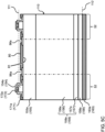
- Fig. 2C shows a vertical cross section of the turn-off power semiconductor device 100 along a line I-I' in Fig. 2B
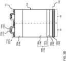
- Fig. 2D shows a vertical cross section of the turn-off power semiconductor device 100 along a line II-II' in Fig. 2B .
- the turn-off power semiconductor device 100 comprises a semiconductor wafer 110 having a first main side 111 and a second main side 112 opposite to the first main side 111.
- the first main side 111 and the second main side 112 of the semiconductor wafer 110 shall respectively be understood as a plane including the outermost flat surface portions of the semiconductor wafer 110 on two opposite sides.
- Integrated in the semiconductor wafer 110 is a plurality of thyristor cells 51, 52 comprising first thyristor cells 51 and second thyristor cells 52.
- Each of the first thyristor cells 51 comprises in an order from the first main side 111 to the second main side 112 an n + -type first emitter layer portion 154a, a p-type first base layer portion 155a, an n-type second base layer portion 159a, and a p + -type second emitter layer portion 158a.
- the first emitter layer portion 154a is in direct contact with the first base layer portion 155a to form a first p-n junction between the first base layer portion 155a and the first emitter layer portion 154a.
- the first base layer portion 155a is in direct contact with the second base layer portion 159a to form a second p-n junction between the first base layer portion 155a and the second base layer portion 159a, and the second emitter layer portion 158a is separated from the first base layer portion 155a by the second base layer portion 159a.
- the second base layer portion 159a is in direct contact with the second emitter layer portion 158a to form a third p-n junction between the second base layer portion 159a and the second emitter layer portion 158a.
- the second base layer portion 159a may comprise a drift layer portion 156a and a buffer layer portion 157a separating the second emitter layer portion 158a from the drift layer portion 156a.
- the buffer layer portion 157a has a higher doping concentration than the drift layer portion 156a. It may have a rising doping concentration towards the second main side 112, whereas the drift layer portion 156a may have a constant doping concentration.
- Each first thyristor cell 51 further comprises a first gate electrode layer portion 161a, a first main electrode layer portion 162a and a second main electrode layer portion 163a.
- the first gate electrode layer portion 161a is arranged lateral to the first emitter layer portion 154a and forms an ohmic contact with the first base layer portion 155a.
- the first main electrode layer portion 162a is arranged on the first main side 111 and forms an ohmic contact with the first emitter layer portion 154a.
- the second main electrode layer portion 163a is arranged on the second main side 112 and forms an ohmic contact with the second emitter layer portion 158a.
- the first gate electrode layer portions 161a of all first thyristor cells 51 are implemented as a first gate electrode layer 161.
- the second thyristor cells 52 have basically the same structure as the first thyristor cells 51.
- Fig. 2D shows the structure of two second thyristor cells 52 in cross section. Same reference signs therein refer to elements that have the same features and characteristics as described above for the first thyristor cells 51. Accordingly, it is referred to the description of the first thyristor cells 51 above.
- Second gate electrode layer portions 171a of the second thyristor cells 52 are arranged lateral to the first emitter layer portions 154a of the second thyristor cells 52 and form an ohmic contact with the first base layer portions 155a, respectively.
- the second gate electrode layer portions 171a of all second thyristor cells 52 are implemented as a second gate electrode layer 171.
- the first thyristor cells 51 are arranged in three concentric rings in a plane parallel to the second main side 112 and adjacent to a circumferential edge of the semiconductor wafer 110. Accordingly, in the top view in Fig. 2A the first main electrode layer portions 162a of the first thyristor cells 51 are arranged in three concentric rings and a white area surrounding the first main electrode layer portions 162a of the first thyristor cells 51 corresponds to the first gate electrode layer 161 laterally surrounding the first main electrode layer portions 162a of all first thyristor cells 51.
- the second thyristor cells 52 are arranged in three concentric rings in a plane parallel to the second main side 112 and in a central region of the semiconductor wafer 110.
- the three concentric rings of first thyristor cells 51 surround the three concentric rings of second thyristor cells 52.
- first main electrode layer portions 172a of the second thyristor cells 52 are arranged in three concentric rings and are surrounded by the second gate electrode layer 171.
- the semiconductor wafer 110 has a circular shape, the first emitter layer portions 154a of the plurality of thyristor cells (i.e.
- first thyristor cells 51 and of the second thyristor cells 52 are stripe-shaped and are arranged in concentric rings with a longitudinal main axis of the stripe-shaped first emitter layer portions 154a respectively extending along a radial direction extending from a lateral center C of the semiconductor wafer 110.
- a common gate contact 60 is arranged on the first main side 111.
- the common gate contact 60 has a ring-shape and extends along the circumferential edge of the semiconductor wafer 110.
- all first emitter layer portions 154a have the same distance from the common gate contact 60.
- the first emitter layer portion 154a of each first thyristor cell 51 has a distance from the common gate contact 60 that is smaller than a predetermined distance
- the first emitter layer portion of each second thyristor cell 52 has a distance from the common gate contact 60 that is larger than the predetermined distance. That means that all first emitter layer portions 154a of all first thyristor cells 51 have a smaller distance from the common gate contact 60 than any first emitter layer portion 154a of each second thyristor cell 52.
- the first gate electrode layer 161 is directly connected to the common gate contact 60 such that the first gate electrode layer portion 161a of each first thyristor cell 51 is electrically connected to the common gate contact 60 by an electrical path inside of the first gate electrode layer 161.
- a plurality of stripe-shaped, electrically conductive first gate runners 70 is arranged on the semiconductor wafer 110 at the first main side 111.
- the first gate runners 70 can be seen in top view, whereas in Fig. 2C a first gate runner 70 is shown in cross section.
- Each first gate runner 70 has a first end portion 70a, a second end portion 70b opposite to the first end portion 70a and a first connecting portion 70c connecting the first end portion 70a and the second end portion 70b.
- the first end portion 70a is directly connected to the common gate contact 60 and a longitudinal main axis MA1 of each first gate runner 70 is extending in a lateral direction away from the common gate contact 60.
- each first gate runner 70 extends from the circular, ring-shaped common gate contact 60 in a radial direction inwards towards a lateral center C of the semiconductor wafer 110.
- the second end portion 70b of each first gate runner 70 is directly connected to the second gate electrode layer 171.
- the first gate runners 70 are laterally arranged with rotational symmetry as shown in Fig. 2A .
- At least the first connecting portion 70c of each first gate runner 70 is separated from the first gate electrode layer 161, so that any electrically conducting path from the first connecting portion 70c of each first gate runner 70 to the first gate electrode layer 161 passes at least through one of the first end portion 70a of the same first gate runner 70, the second end portion 70b of the same first gate runner 70 and the semiconductor wafer 110.
- black lines along the two lateral sides of each first gate runner 70 show the separation of the first gate runner 70 from the first gate electrode layer 161. Gaps on two opposing lateral sides of the first gate runners 70 between the first gate electrode layer 161 and the first connecting portion 70c of each first gate runner 70 are indicated as first separation lines 95a in Fig. 2B .
- the second gate electrode layer 171 comprises a first ring-shaped gate electrode layer portion 171b, which is laterally surrounding the remaining portion of the second gate electrode layer 171.
- Each first gate runner 70 connects the common gate contact 60 with this first ring-shaped electrode layer portion 171b. Any point in the second gate electrode layer 171 is electrically connected to the first ring-shaped electrode layer portion 171b by an electrical path inside of the second gate electrode layer 171. That means that any second gate electrode layer portion 171a of the second thyristor cells 52 is directly electrically connected to the first ring-shaped gate electrode layer portion 171b.
- each one of the first gate electrode layer 161, the second gate electrode layer 171, the common gate contact 60 and the first gate runners 70 comprises a metal material such as aluminium.
- the first gate runners 70 have a length in radial direction that is at least two or at least three times a maximal length of the first emitter layer portions 154a of any first thyristor cell 51. Accordingly the first gate runners 70 traverse plural rings of the first emitter layer portions 154a in a top view.
- the first emitter layer portions 154a of all thyristor cells 51, 52 belong to a first emitter layer 154
- the first base layer portions 155a are portions of a continuous first base layer 155
- the second base layer portions 159a are portions of a continuous second base layer 159
- the drift layer portions 156a are portions of a continuous drift layer 156
- the buffer layer portions 157a are portions of a continuous buffer layer 157
- the second emitter layer portions 158a are portions of a continuous emitter layer 158
- the second main electrode layer portions 163a are portions of a continuous second main electrode layer 163.
- first emitter layer 154, the first base layer 155, the second base layer 159, the drift layer 156, the buffer layer 157, the second emitter layer 158 and the second main electrode layer 163 may be shared by the first and second thyristor cells 51, 52.
- a thickness d2 of each first gate runner 70 in a direction perpendicular to the lateral direction may be the same or may alternatively be at least 25% or at least 50% higher than a thickness d1 of the first gate electrode layer 161 at a position in the middle between two adjacent first emitter layer portions 154a.
- a turn-off power semiconductor device 200 according to a second embodiment that does not fall under the scope of the claimed invention, will be discussed with reference to Fig. 3 which shows the turn-off power semiconductor device 200 in cross-section. Due to the many similarities between the turn-off power semiconductor device 100 according to the first embodiment and the turn-off power semiconductor device 200 according to the second embodiment only differences between the second embodiment and the first embodiment will be discussed in the following, whereas it is referred to the above discussion of the first embodiment with regard to all remaining features. In particular, if reference signs used in Fig. 3 are identical to reference signs used in any one of figures 2A to 2D , then they refer to same elements having the same features and characteristics as in the first embodiment.
- the top view of the turn-off power semiconductor device 200 is the same as the top view of the turn-off power semiconductor device 100 as shown in Fig. 2A .
- the cross-section shown in Fig. 3 is a cross section along line I-I' in Fig. 2B .
- the only difference between the first and the second embodiment is that in the second embodiment the first gate runners 70 are respectively separated and electrically insulated from the semiconductor wafer 110 by an insulating layer 75 interposed between each first gate runner 70 and the semiconductor wafer 110.
- the insulating layer 75 is interposed between a bottom 71 of each first gate runner 70 and the first base layer 155.
- a thickness d2 of each first gate runner 70 in a direction perpendicular to the lateral direction may be the same or may alternatively be at least 25% or at least 50% higher than a thickness d1 of the first gate electrode layer 161 at a position in the middle between two adjacent first emitter layer portions 154a.
- a turn-off power semiconductor device 300 according to a third embodiment, a first embodiment that falls under the scope of the claimed invention, is discussed with reference to Fig. 4 which shows a section of a top view of the turn-off power semiconductor device 300. Due to the many similarities between the turn-off power semiconductor device 300 of the third embodiment and the turn-off power semiconductor device 100 according to the first embodiment, only differences between the third embodiment and the first embodiment are discussed in the following, whereas it is referred to the discussion of the first embodiment above with regard to all remaining features. In particular, reference signs in Fig. 4 which are identical to reference signs used in anyone of figures 2A to 2D refer to same elements having the same features and the same characteristics as described above for the first embodiment.
- a cross section of the turn-off power semiconductor device 300 along a line I-I' in Fig. 4 is identical to the cross section shown in Fig. 2B above.
- the first ring-shaped gate electrode layer portion 171b of the second gate electrode layer 171 is separated from the first gate electrode layer 161 in a radial direction.
- a gap between the first ring-shaped gate electrode layer portion 171b and the first gate electrode layer 161 is indicated by a second separation line 95b shown in Fig. 4 .
- the second separation line 95b connects two adjacent first separation lines 95a so that two adjacent first separation lines 95a and the connecting second separation line 95b form a single continues separation line.
- a direction perpendicular to the second separation line 95b there is no direct contact between the second gate electrode layer 171 and the first gate electrode layer 161.
- a gate current from the second thyristor cells 52 is prevented from flowing into the first gate electrode layer 161 and is forced to flow through the first gate runners 70 towards the common gate contact 60.
- FIG. 5A shows a top view of the turn-off power semiconductor device 400.
- Fig. 5B shows an enlarged view of section B in Fig.
- First thyristor cells 51 are arranged in the two outermost concentric rings and first gate runners 70 traverse these two concentric rings in a radial direction.
- the first end portion 70a of each first gate runner 70 is connected to the common gate contact 60 and the second end portion 70b of each first gate runner 70 is connected to the first ring-shaped gate electrode layer portion 171b of the second gate electrode layer 171 as in the first embodiment.
- the first thyristor cells 51 in the fourth embodiment are arranged in only two concentric rings, whereas in the first embodiment the first thyristor cells 51 are arranged in three outermost concentric rings.
- Second thyristor cells 52 in the fourth embodiment are arranged in two intermediate concentric rings.
- Second gate runners 80 traverse the two concentric rings of second thyristor cells 52 in a radial direction from the first ring-shaped gate electrode layer portion 171b to a second ring-shaped gate electrode layer portion 181b of a third gate electrode layer 181 discussed below.
- Each second gate runner 80 has, similar to the first gate runners 70, a third end portion 80a, a fourth end portion 80b opposite to the third end portion 80a and a second connecting portion 80c connecting the third end portion 80a and the fourth end portion 80b.
- each second gate runner 80 is connected to the first ring-shaped electrode layer portion 171b and the fourth end portion 80b of each second gate runner 80 is connected to the second ring-shaped electrode layer portion 181b.
- At least the second connecting portion 80c of each second gate runner 80 is separated from the second gate electrode layer 171 so that any electrically conducting path from the second connecting portion 80c of each second gate runner 80 to the second gate electrode layer 171 passes at least through one of the third end portion 80a of the same second gate runner 80, the fourth end portion 80b of the same second gate runner 80 and the semiconductor wafer 110.
- Gaps between the second connecting portion 80c and the second gate electrode layer 171 along two lateral sides of the connection portion 80c are indicated as third separation lines 96a in Fig. 5B .
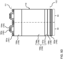
- Fig. 5C there is shown a cross-section along a line II-II' in Fig. 5B .
- Two second thyristor cells 52 and a gate runner 80 laterally interposed between these two second thyristor cells 52 can be seen in cross-section in Fig. 5C .
- Third thyristor cells 53 are laterally arranged in two innermost concentric rings. A cross-section of two adjacent third thyristor cells 53 along a line III-III' in Fig. 5B is shown in Fig. 5D . Except that the third thyristor cells 53 are arranged in two innermost concentric rings, whereas the second thyristor cells 52 in the first embodiment are arranged in three innermost concentric rings, the lateral arrangement and the structure of the third thyristor cells 53 in the fourth embodiment is the same as the lateral arrangement and structure of second thyristor cells 52 in the first embodiment.
- the stripe-shaped first emitter layer portions 154a of the third thyristor cells 53 are laterally surrounded by the third gate electrode layer 181 which includes third gate electrode layer portions 181a of all third thyristor cells 53.
- the second ring-shaped gate electrode layer portion 181b surrounds a remaining portion of the third gate electrode layer 181.
- the second gate runners 80 have a similar structure as the first gate runners 70. The only difference is that the second gate runners 80 are not directly connected to the common gate contact 60 at its third end portion 80a, respectively, but are connected to the first ring-shaped gate electrode layer portion 171b. As can be seen best from Fig. 5A , the number of first gate runners 70 is higher than the number of second gate runners 80.
- Each second gate runner 80 has a longitudinal main axis MA2 which is aligned to the longitudinal main axis MA1 of one of the first gate runners 70. In this manner pairs of a first gate runner 70 and of a second gate runner 80, respectively, form linear electrically conductive paths to connect the common gate contact 60 to the second ring-shaped gate electrode layer portion 181b.
- a turn-off power semiconductor device 500 according to a fifth embodiment a further embodiment that falls under the scope of the claimed invention, will be described with reference to Fig. 6 . Due to many similarities between turn-off power semiconductor device 500 according to the fifth embodiment and the turn-off power semiconductor devices 300 and 400 according to the third and fourth embodiment only differences between these embodiments will be described in the following.
- Fig. 6 shows a section B of the top view of the turn-off power semiconductor device 500, which corresponds to the top view shown in Fig. 5A .
- the fifth embodiment 500 also differs from the first, second and fourth embodiments in that the second gate electrode layer 171 is separated from the first gate electrode layer 161 in a radial direction as in the third embodiment shown in Fig 4 .
- a gap between the first ring-shaped gate electrode layer portion 171b and the first gate electrode layer 161 is indicated by a second separation line 95b in Fig. 6 .
- the second separation line 95b connects two adjacent first separation lines 95a as in the third embodiment. In a direction perpendicular to the second separation line 95b there is no direct contact between the second gate electrode layer 171 and the first gate electrode layer 161. As a result a gate current from the second thyristor cells 52 is prevented from flowing into the first gate electrode layer 161 and is forced to flow through the first gate runners 70 towards the common gate contact 60.
- the third gate electrode layer 181 is separated from the second gate electrode layer 171 in a radial direction.
- a gap between the second ring-shaped gate electrode layer portion 181b and the second gate electrode layer 171 is indicated by a fourth separation line 96b.
- the sixth embodiment differs from the fifth embodiment only in that the innermost ring of first thyristor cells 51 has first emitter layer portions 154a and corresponding first main electrode layer portions 162a, in which a length of the first emitter layer portions 154a varies as a function of a distance to the next first gate runner 70 along a circular direction (perpendicular to the radial direction), such that any first emitter layer portion 154a adjacent to any one of the first gate runners 70 has a shorter length than all other first emitter portions in this innermost ring which are not adjacent to one of the first gate runners 70 in the circular direction.
- the length of the first emitter layer portions 154a increases continuously with increasing distance from the next first gate runner 70 such that a distance of the first emitter layer portions 154a in the innermost ring to the respective next first emitter layer portion 154a of a second thyristor cell 52 increases with increasing distance to the next first gate runner 70.
- a radial width of the first ring-shaped gate electrode layer portion 171b varies and increases along a circumferential direction towards the first gate runners 70, i.e. the radial width of the first ring-shaped gate electrode layer portion 171b is larger the closer the circumferential position is to the next first gate runner 70.
- the same variation of the length of the first emitter layer portions 154a applies to the innermost ring of second thyristor cells 52.
- the turn-off power semiconductor device may be a reverse conducting turn-off power semiconductor device, i.e. it may comprise a freewheeling diode integrated in the semiconductor wafer.
- the above described turn-off power semiconductor devices were described to comprise a drift layer 156 and a buffer layer 157. However, the turn-off power semiconductor device does not necessarily comprise a buffer layer.
- first, second and third thyristor cells 51, 52 and 53 in plural concentric rings.
- the thyristor cells may be arranged in another way.
- the number of rings in which the first to third thyristors cells are arranged may be different from the number of rings shown in the figures.
- the common gate contact 60 is arranged to extend along the circumferential edge of the semiconductor wafer 110.
- the common gate contact 60 may have another shape. Also it may be arranged at another position such as in the lateral center region of the semiconductor wafer or as a ring-shaped region laterally interposed between thyristor cells outside of the ring-shaped region and thyristor cells inside of the ring-shaped region.
- the innermost rings of both, of the first thyristor cells 51 and of the second thyristor cells 52 were described to have a varying length of the first emitter layer portions 154a.
- the innermost ring of the first emitter cells 51 or of the second emitter cells 52 may have a variation of the length of first emitter layer portions 154.
- first separation lines 95a were described as a gap in a lateral direction.
- the separation between the first connection portion 70c and the first gate electrode layer 161 may also be implemented without such gap by an insulating layer interposed between the first gate electrode layer 161 and the first connecting portion 70c.
- the turn-off power semiconductor deviced 400, 400 and 500 were described with two different groups of thyristor cells, namely the first thyristor cells 51 and the second thyristor cells 52, which are traversed by different number of gate runners 70 and 80, respectively. However, there may exist further groups of thyristor cells which are traversed by additional gate runners.
Landscapes
- Thyristors (AREA)
Description
- The present invention relates to a turn-off power semiconductor device comprising a plurality of thyristor cells which are all connected to a common gate contact.
- Document
CN 104 600 101 A discloses a dual-gate-electrode contact ring cathode surface layer structure of an integrated gate electrode commutation thyristor chip. -
Document EP 2 930 753 A1 discloses a turn-off power semiconductor device comprising a plurality of thyristor cells. - Document
US 6 570 193 B1 discloses a reverse conducting thyristor device, aiming at preventing heat generated by power loss from filling end field protective rubber and at simplifying a sheath storing a semiconductor substrate. - Document
EP 0 592 991 A1 discloses a GTO thyrisor, wherein a cathode-side emitter fingers are arranged in a plurality of mutually concentric rings. - Document
JP H04 320374 A - In the field of power semiconductor devices there is known a turn-off power semiconductor device such as a gate commutated thyristor (GCT) power device, in particular an integrated gate commutated thyristor (IGCT). In a reverse conducting (RC) IGCT a freewheeling diode may be integrated in the device wafer.
- As an example for a GCT power device a prior art RC-IGCT 1 is shown in
Figures 1A and 1B . Such RC-IGCT is described for example inWO 2012/041958 A2 .Fig. 1A illustrates a portion of the known RC-IGCT 1 in cross section andFig. 1B shows the layout of the device in top view. The RC-IGCT 1 comprises a plurality ofthyristor cells 2 and an integrated free-wheeling diode 3. Allthyristor cells 2 and the integrated free-wheeling diode 3 are formed in onesingle wafer 10 having a firstmain side 11, which is the cathode side of the RC-IGCT 1, and a secondmain side 12, which is the anode side of the RC-IGCT 1. - As can be seen in
Fig. 1A , eachthyristor cell 2 comprises from the firstmain side 11 to the secondmain side 12 of the wafer 10 afirst cathode electrode 21, an n+-doped cathodesemiconductor layer portion 22, a p-dopedbase semiconductor layer 23, an n--dopeddrift semiconductor layer 24, an n-dopedbuffer semiconductor layer 25, a p+-doped firstanode semiconductor layer 26 and afirst anode electrode 27. The cathodesemiconductor layer portions 22 of the plurality ofthyristor cells 2 form a first cathode semiconductor layer. Therein thebuffer semiconductor layer 25 has a rising doping concentration towards the secondmain side 12, whereas thedrift semiconductor layer 24 has typically a constant doping concentration. - Further, each
thyristor cell 2 has agate electrode 20 which is arranged on the firstmain side 11 of thewafer 10 lateral to the cathodesemiconductor layer portion 22 and contacting thebase semiconductor layer 23, but separated from thefirst cathode electrode 21 and the cathodesemiconductor layer portion 22. Therein, the term "lateral" relates to the position in a lateral direction which is a direction parallel to the firstmain side 11. - In the circumferential edge region of the
wafer 10 there is arranged the integrated single free-wheeling diode 3, a cross section of which along the line AA' inFig. 1B can also be seen inFig. 1A . The free-wheeling diode 3 comprises from the firstmain side 11 to the secondmain side 12 of the wafer 10 asecond anode electrode 31, a p-doped secondanode semiconductor layer 32, an n+-doped secondcathode semiconductor layer 33, which is separated from the p-doped secondanode semiconductor layer 32 by the n--dopeddrift semiconductor layer 24, and asecond cathode electrode 34. - The arrangement of the plurality of
thyristor cells 2 in the RC-IGCT 1 is illustrated inFig. 1B which shows a top view onto the firstmain side 11 of thewafer 10. The cathodesemiconductor layer portions 22 of the RC-IGCT 1 are formed in the shape of strips with its longitudinal direction aligned in a radial direction which is a direction extending from a lateral center of thecircular wafer 10 and being parallel to the firstmain side 11 of thewafer 10. Further, strips shall be understood as layers, which have in one direction, which is their longitudinal direction, a longer extension than in the other directions by having two longer sides, which are typically arranged parallel to each other. The plurality of strip-shaped cathodesemiconductor layer portions 22 are arranged in concentric rings around the center of the device. In the center region of thewafer 10 there is arranged acommon gate contact 40 to which allgate electrodes 20 of the plurality ofthyristor cells 2 are electrically connected. Thegate electrodes 20 of thethyristor cells 2, thecommon gate contact 40 and the connections there between are implemented as a gate metallization layer surrounding all the cathodesemiconductor layer portions 22. - For turning off the RC-IGCT, a short control gate current pulse is supplied through the
common gate contact 40 to thegate electrodes 20 of the plurality ofthyristor cells 2. The uniformity of the current distribution to the plurality ofthyristor cells 2 is an important parameter for the turn-off performance of the RC-IGCT 1. In the RC-IGCT described above withFigures 1A and 1B , thecommon gate contact 40 is located on the firstmain side 11 in the center thereof. Thethyristor cells 2 in an outer ring are turned off by a lower gate current than thyristor cells of an inner ring. Therefore the charge under the cathodesemiconductor layer portions 22 of an inner ring is removed faster than that under the cathodesemiconductor layer portions 22 of an outer ring. Accordingly, thethyristor cells 2 of an outer ring remain in an on-state longer and consequently can be overloaded, what may finally result in destruction of the whole device. The same problem of non-uniform turn-off ofthyristor cells 2 due to an inhomogeneous gate current distribution exists not only for the RC-IGCT 1 but also for any other turn-off semiconductor power device comprising a plurality of thyristor cells. - To homogenize the current distribution it is known a turn-off power semiconductor device where the common gate contact has the shape of a concentric ring located on the first main side at the perimeter of the wafer. In another turn-off power semiconductor device as described in
EP 0 592 991 A1 , the common gate contact is located between two rings of thyristor cells somewhere between the center and the perimeter of the device. This known approaches have, however, the disadvantage that they can only alleviate the local inhomogeneities of the gate current pulse to the plurality of thyristor cells but cannot avoid them. - IGCT wafers normally do not display a linear relationship between the device area and the maximal controllable current, because of the unavoidable impedance increase in the gate circuit when the device area increases. A common approximation is that the controllable current scales linearly with the device diameter, or the square-root of the device area. For very large devices (>70 mm in diameter), this effect can become limiting in operation, because most other parameters scale linearly with the device area. For example, on-state losses and thermal resistance both scale down linearly with device area and would facilitate a linear increase of the current.
- Increasing the device area leads to the distances over the wafer increasing as well. The distances translate into increased impedance within the gate metallisation layer, both resistive and inductive. Consequently, the farthest region of the wafer, measuring from the gate contact, experience the highest impedance in the gate circuit. In addition, the closer regions of the gate metallisation are loaded with higher gate current because the different regions of the gate metallisation are normally connected in series.
- From
EP 2930753 A1 there is known a turn-off power semiconductor device comprising a plurality of thyristor cells, in which the distance between a gate electrode and a cathode semiconductor layer portion in a thyristor cell depends on the distance of the thyristor cell from a common gate contact. Specifically, for each pair of a first thyristor cell and a second thyristor cell of the plurality of thyristor cells, for which the distance between the first thyristor cell and the common gate contact is smaller than the distance between the second thyristor cell and the common gate contact, a minimum distance between the gate electrode and the cathode semiconductor layer portion is smaller in the second thyristor cell than in the first thyristor cell. The decreasing distance between gate electrode and the cathode semiconductor layer portion in a thyristor cell with increasing distance of the thyristor cells from the common gate contact results in a decreasing serial resistance of the base semiconductor layer connecting the gate electrode to the cathode semiconductor layer portion. In this way the decreased distance between the gate electrode and the cathode semiconductor layer portion with increasing distance of the thyristor cells from the common gate contact can compensate the increasing voltage drop with increasing distance from the common gate contact. However, while the inhomogeneities of the gate current density in the device can be avoided and the thyristor cells can be turned off at the same time to improve the turn-off performance of the turn-off power semiconductor device, at the same time increasing the distance between gate electrode and the cathode semiconductor layer portion in a thyristor cell increases the impedance which results in slower commutation of the conduction current from the cathode to the gate. Especially for large wafers this becomes a severe problem and this concept cannot be applied because the large impedance may prevent turn-off by commutation. - In
CN 104600101 A it is disclosed an IGCT comprising a gate electrode layer that has two concentric rings separated by plural concentric rings of thyristor cells, wherein the two concentric rings of the gate electrode layer are connected to each other through radial gate electrode strips. It is, however, not disclosed any separation or decoupling of the radial gate electrode strips from the remaining gate electrode layer at its sides, so that the inductance distribution may still be unbalanced. - From
US 6 570 193 B1 it is known a reverse conducting thyristor device. It aims at preventing heat generated by power loss from filling end field protective rubber and at simplifying a sheath storing a semiconductor substrate. In a reverse conducting thyristor device according to this invention, a self-extinguishing thyristor region is arranged on an inner region of the semiconductor substrate, a reverse conducting diode region whose outer periphery is completely enclosed with an isolation region is arranged on its outer region by at least one, and an external takeout gate electrode region is further arranged on the outermost peripheral region of the semiconductor substrate on the outer part thereof. Thus, a gate electrode provided on a surface of a gate part layer of the self-extinguishing thyristor region is connected with an external takeout gate electrode formed along the outermost periphery of the substrate through a gate wiring pattern formed on a surface of a connecting region. - In view of the above, it is the object of the invention to provide a turn-off power semiconductor device which allows to reliably control a large current.
- The object of the invention is attained by a turn-off power semiconductor device according to
claim 1. Further developments of the invention are specified in the dependent claims. - The turn-off power semiconductor device according to
claim 1 comprises a semiconductor wafer having a first main side and a second main side opposite to the first main side, a plurality of thyristor cells, a common gate contact arranged on the first main side and a plurality of stripe-shaped electrically conductive first gate runners. Throughout the specification an element having a stripe-shaped shall mean an element that has along a longitudinal main axis thereof a length with is at least twice a length in any direction perpendicular to the longitudinal main axis. Each first gate runner has a first end portion, a second end portion opposite to the first end portion and a first connecting portion connecting the first end portion and the second end portion. The first end portion is directly connected to the common gate contact and a longitudinal main axis of each first gate runner is extending in a lateral direction away from the common gate contact. Each thyristor cell comprises in an order from the first main side to the second main side a first emitter layer portion of a first conductivity type, a first base layer portion of a second conductivity type different from the first conductivity type, a second base layer portion of the first conductivity type, and a second emitter layer portion of the second conductivity type. The first emitter layer portion is in direct contact with the first base layer portion to form a first p-n junction between the first base layer portion and the first emitter layer portion. The first base layer portion is in direct contact with the second base layer portion to form a second p-n junction between the first base layer portion and the second base layer portion. The second emitter layer portion is separated from the first base layer portion by the second base layer portion, wherein the second base layer portion is in direct contact with the second emitter layer portion to form a third p-n junction between the second base layer portion and the second emitter layer portion. Each thyristor cell further comprises a gate electrode layer portion which is arranged lateral to the first emitter layer portion and forms an ohmic contact with the first base layer portion, a first main electrode layer portion which is arranged on the first main side and forms an ohmic contact with the first emitter layer portion, and a second main electrode layer portion which is arranged on the second main side and forms an ohmic contact with the second emitter layer portion. The plurality of thyristor cells comprises first thyristor cells and second thyristor cells. The first emitter layer portion of each first thyristor cell has a distance from the common gate contact that is smaller than a predetermined distance. The first emitter layer portion of each second thyristor cell has a distance from the common gate contact that is larger than the predetermined distance. The distances shall be measured as a minimum lateral distance between the layers or contacts. The gate electrode layer portions of all first thyristor cells are implemented as a first gate electrode layer. The gate electrode layer portions of all second thyristor cells are implemented as a second gate electrode layer. The first gate electrode layer is directly connected to the common gate contact such that the gate electrode layer portion of each first thyristor cell is electrically connected to the common gate contact. The second end portion of each first gate runner is directly connected to the second gate electrode layer. At least the first connecting portion of each first gate runner is separated from the first gate electrode layer, so that any electrically conducting path from the first connecting portion of each first gate runner to the first gate electrode layer passes at least through one of the first end portion of the same first gate runner, the second end portion of the same first gate runner and the semiconductor wafer. - Throughout the specification, a lateral direction shall be understood as a direction parallel to the second main side. In case of an uneven second main side, a lateral direction parallel to the second main side is to be understood as a direction parallel to a reference plane for which the arithmetic mean value of a distance between the second main side and the reference plane is minimal (compared to all other planes), wherein the arithmetic mean value is calculated from the distance values of all points on the second main side. Throughout the specification the term lateral shall refer to such defined lateral direction. Exemplarily, if one element is described to be arranged lateral to another element, then it is arranged at a position which is shifted from the position of the other element in the lateral direction as defined above.
- The first gate runners in the turn-off power semiconductor device of the invention provide efficient means for reducing the impedance of the electrical connection between the common gate contact and the gate electrode layer portions of the second thyristor cells. Due to the separation of the connecting portion from the first gate electrode layer, the gate runners are not loaded with gate current for the first thyristor cells. This allows to turn off a current flowing through the second thyristor cells by commutation efficiently even if the second thyristor cells are far away from the common gate contact so that the turn-off power semiconductor device of the invention can be implemented with a large device area to thereby achieve a reliable control of a relatively large current.
- The common gate contact is ring-shaped in an orthogonal projection onto a plane parallel to the second main side and the longitudinal main axis of each first gate runner extends in a radial direction from the common gate contact towards a lateral center of the semiconductor wafer. In this arrangement the gate control is especially efficient because a relatively large device area at the circumferential edge of the semiconductor wafer has a small distance to the common gate contact, while only a relatively small device area in the lateral center region of the semiconductor wafer has a relatively large distance to the common gate contact, wherein the thyristor cells in the central region of the semiconductor wafer are connected to the common gate contact through the first gate runners.
- In an orthogonal projection onto a plane parallel to the second main side, a first ring shaped gate electrode layer portion of the second gate electrode layer is arranged inside the ring-shaped common gate contact to laterally surround the remaining portion of the second gate electrode layer, wherein each first gate runner connects the common gate contact with the first ring-shaped electrode layer portion. This arrangement allows most efficient gate control of the second thyristor cells.
- Also, the first ring-shaped gate electrode layer portion is separated from the first gate electrode layer so that any electrically conducting path from the second gate electrode layer passes at least through the semiconductor wafer or through one of the first gate runners. Accordingly, an electrical path for the gate current for the first thyristor cells is most efficiently decoupled from an electrical path for the gate current for the second thyristor cells.
- In an exemplary embodiment each one of the first gate electrode layer, the second gate electrode layer, the common gate contact and the first gate runners comprise a metal material. The metal material has a significantly larger electrical conductivity than the semiconductor material so that the impedance of any electrical path from the common gate contact to any gate electrode layer portion is relatively low.
- In an exemplary embodiment, the plurality of thyristor cells comprise third thyristor cells, wherein the first emitter layer portion of each third thyristor cell has a distance from a common gate contact that is greater than a distance of each one of the first emitter layer portions of the first thyristor cells and greater than a distance of each one of the second thyristor cells from the common gate contact. The gate electrode layer portions of all third thyristor cells are implemented as a third gate electrode layer. A second ring-shaped gate electrode layer portion of the third gate electrode layer is arranged inside of the ring-shaped common gate contact to laterally surround the remaining portion of the third gate electrode layer. The first gate electrode layer and the second gate electrode layer are both arranged outside of the second ring-shaped gate electrode layer portion. The turn-off power semiconductor device according to this exemplary embodiment further comprises a plurality of stripe-shaped electrically conductive second gate runners, each second gate runner having a third end portion, a fourth end portion opposite to the third end portion and a second connecting portion connecting the third end portion and the fourth end portion. The third end portion of each second gate runner is connected to the first ring-shaped electrode layer portion and the fourth end portion of each second gate runner is connected to the second ring-shaped electrode layer portion. At least the second connecting portion of each second gate runner is separated from the second gate electrode so that any electrically conducting path from the second connecting portion of each second gate runner to the second gate electrode layer passes at least through one of the third end portion of the same second gate runner, the fourth end portion of the same second gate runner and the semiconductor wafer. In this exemplary embodiment the gate control of second thyristor cells is facilitated by the first gate runners and the gate control of the third thyristor cells is facilitated by the first and second gate runners.
- In the latter exemplary embodiment, the number of first gate runners may be higher than the number of second gate runners. In this manner inhomogeneities of the gate current density in the device can be avoided and the first, second and third thyristor cells can be turned off at the same time to improve the turn-off performance of the turn-off semiconductor device.
- A longitudinal main axis of each second gate runner may be aligned with the longitudinal main axis of one of the first gate runners. In this manner the impedance of an electrical path from the gate electrode portions of third thyristor cells to the common gate contact can be further reduced.
- In an exemplary embodiment, the semiconductor wafer has a circular shape in an orthogonal projection onto a plane parallel to the second main side. Also, in the orthogonal projection the first emitter layer portions of the plurality of thyristor cells are stripe-shaped and are arranged in concentric rings with a longitudinal main axis of the stripe-shaped first emitter layer portions respectively extending along a radial direction extending from a lateral center of the semiconductor wafer, wherein in each ring all first emitter layer portions have the same distance from the lateral center. In this exemplary embodiment efficient gate control of all thyristor cells is facilitated.
- In an exemplary embodiment, a length of the first emitter layer portions in an innermost ring varies as a function of a distance to the next first gate runner (along the innermost ring, i.e. along a line extending in a direction perpendicular to the radial direction), such that any first emitter layer portion adjacent to anyone of the first gate runners has a shorter length than all other first emitter portions in this innermost ring which are not adjacent to one of a first gate runners. Such arrangement allows to further reduce the impedance of an electrical path from the gate electrode layer portions of second thyristor cells to the common gate contact. Therein, the next first gate runner is that first gate runner of the plurality of stripe-shaped electrically conductive first gate runners which has the minimal distance to the respective first emitter layer portion. Throughout the specification, if there is a plurality of first elements, a first element next to a second element ("next first element") means that first element of the plurality of first elements that has the minimal distance to the second element. Also, if there is a plurality of first elements, a first element adjacent to a second element ("adjacent first element') means that there is no other first element between the adjacent first element and the second element.
- In the later exemplary embodiment, the length of the first emitter layer portions in the innermost ring may increase with increasing distance from the next first gate runner such that a distance of the first emitter layer portions in the innermost ring to the respective next first emitter layer portion of a second thyristor cell increases with increasing distance to the next first gate runner.
- In an exemplary embodiment, a length of each first gate runner in a radial direction is at least two or at least three times a maximal length of the first emitter layer portions of any first thyristor cell.
- In an exemplary embodiment, a thickness of each first gate runner in a direction perpendicular to the lateral direction is at least 25% higher or at least 50% higher than a thickness of the first gate electrode layer at a position in the middle between two adjacent first emitter layer portions, wherein a thickness direction is a direction perpendicular to the second main side. This may further reduce the impedance of the first gate runners to further improve gate control of the second thyristor cells, while the relatively thin first gate electrode layer allows small distances between neighbouring first emitter layer portions of the first thyristor cells.
- In an exemplary embodiment, the first gate runner is separated and electrically insulated from the semiconductor wafer by an insulating layer interposed between the the first gate runner and the semiconductor wafer. Such electrical insulation of the first gate runners from the semiconductor wafer further facilitates gate control of the second thyristor cells.
- In an exemplary embodiment, the first and/or second gate runners are laterally arranged with rotational symmetry. Such arrangement may reduce the inhomogeneities of the gate current density in the device and the thyristor cells can be turned off at the same time to improve the turn-off performance of the turn-off power semiconductor device.
- Detailed embodiments will be explained below with reference to the accompanying figures in which:
- Fig. 1A
- is a cross-section of a turn-off power semiconductor device known from the prior art along a line A-A' in
Fig. 1B ; - Fig. 1B
- is a top view of the turn-off power semiconductor device shown in
Fig. 1A ; - Fig. 2A
- shows a top view of a turn-off power semiconductor device according to a first embodiment (which does as such not fall under the scope of the claims, but serves for a better understanding of certain aspects of the claimed invention);
- Fig. 2B
- shows an enlarged view of section A in the top view of
Fig. 2A ; - Fig. 2C
- is a cross-section of the turn-off power semiconductor device of
Fig. 2A along a line I-I' inFig. 2B ; - Fig. 2D
- is a cross-section of the turn-off power semiconductor device of
Fig. 2A along a line II-II' inFig. 2B ; - Fig. 3
- shows a cross-section of a turn-off power semiconductor device according to a second embodiment (which does as such not fall under the scope of the claims, but serves for a better understanding of certain aspects of the claimed invention);
- Fig. 4
- shows a section of a top view of a turn-off power semiconductor device according to a third embodiment;
- Fig. 5A
- shows a top view of a turn-off power semiconductor device according to a fourth embodiment (which does as such not fall under the scope of the claims, but serves for a better understanding of certain aspects of the claimed invention);
- Fig. 5B
- shows an enlarged view of section B in
Fig. 5A ; - Fig. 5C
- shows a cross-section of the turn-off power semiconductor device according to the fourth embodiment along a line II-II' in
Fig. 5B ; - Fig. 5D
- shows a cross-section of the turn-off power semiconductor device according to the fourth embodiment along a line III-III' in
Fig. 5B ; - Fig. 6
- shows a section of a top view of a turn-off power semiconductor device according to a fifth embodiment; and
- Fig. 7
- shows a section of a top view of a turn-off power semiconductor device according to a sixth embodiment.
- The reference signs used in the figures and their meanings are summarized in the list of reference signs. Generally, similar elements have the same reference signs throughout the specification. The described embodiments are meant as examples and shall not limit the scope of the invention.
- The third, fifth and sixth embodiments are embodiments of the claimed inventions. The first, second and fourth embodiment as shown in
Figures 2A-2D ,3 , and5A-5D do as such not fall under the scope of the claims, but serve for a better understanding of certain aspects of the invention. - In the following a turn-off
power semiconductor device 100 according to a first embodiment, that does not fall under the scope of the claimed invention, is described with reference tofigures 2A ,2B ,2C and2D .Fig. 2A illustrates the turn-offpower semiconductor device 100 in top view,Fig. 2B shows an enlarged view of section A inFig. 2A ,Fig. 2C shows a vertical cross section of the turn-offpower semiconductor device 100 along a line I-I' inFig. 2B , andFig. 2D shows a vertical cross section of the turn-offpower semiconductor device 100 along a line II-II' inFig. 2B . - The turn-off
power semiconductor device 100 comprises asemiconductor wafer 110 having a firstmain side 111 and a secondmain side 112 opposite to the firstmain side 111. The firstmain side 111 and the secondmain side 112 of thesemiconductor wafer 110 shall respectively be understood as a plane including the outermost flat surface portions of thesemiconductor wafer 110 on two opposite sides. Integrated in thesemiconductor wafer 110 is a plurality ofthyristor cells first thyristor cells 51 andsecond thyristor cells 52. - Each of the
first thyristor cells 51 comprises in an order from the firstmain side 111 to the secondmain side 112 an n+-type firstemitter layer portion 154a, a p-type firstbase layer portion 155a, an n-type secondbase layer portion 159a, and a p+-type secondemitter layer portion 158a. The firstemitter layer portion 154a is in direct contact with the firstbase layer portion 155a to form a first p-n junction between the firstbase layer portion 155a and the firstemitter layer portion 154a. The firstbase layer portion 155a is in direct contact with the secondbase layer portion 159a to form a second p-n junction between the firstbase layer portion 155a and the secondbase layer portion 159a, and the secondemitter layer portion 158a is separated from the firstbase layer portion 155a by the secondbase layer portion 159a. The secondbase layer portion 159a is in direct contact with the secondemitter layer portion 158a to form a third p-n junction between the secondbase layer portion 159a and the secondemitter layer portion 158a. Therein, the secondbase layer portion 159a may comprise adrift layer portion 156a and abuffer layer portion 157a separating the secondemitter layer portion 158a from thedrift layer portion 156a. Thebuffer layer portion 157a has a higher doping concentration than thedrift layer portion 156a. It may have a rising doping concentration towards the secondmain side 112, whereas thedrift layer portion 156a may have a constant doping concentration. Eachfirst thyristor cell 51 further comprises a first gateelectrode layer portion 161a, a first mainelectrode layer portion 162a and a second mainelectrode layer portion 163a. The first gateelectrode layer portion 161a is arranged lateral to the firstemitter layer portion 154a and forms an ohmic contact with the firstbase layer portion 155a. The first mainelectrode layer portion 162a is arranged on the firstmain side 111 and forms an ohmic contact with the firstemitter layer portion 154a. The second mainelectrode layer portion 163a is arranged on the secondmain side 112 and forms an ohmic contact with the secondemitter layer portion 158a. The first gateelectrode layer portions 161a of allfirst thyristor cells 51 are implemented as a firstgate electrode layer 161. - The
second thyristor cells 52 have basically the same structure as thefirst thyristor cells 51.Fig. 2D shows the structure of twosecond thyristor cells 52 in cross section. Same reference signs therein refer to elements that have the same features and characteristics as described above for thefirst thyristor cells 51. Accordingly, it is referred to the description of thefirst thyristor cells 51 above. Second gateelectrode layer portions 171a of thesecond thyristor cells 52 are arranged lateral to the firstemitter layer portions 154a of thesecond thyristor cells 52 and form an ohmic contact with the firstbase layer portions 155a, respectively. The second gateelectrode layer portions 171a of allsecond thyristor cells 52 are implemented as a secondgate electrode layer 171. - The
first thyristor cells 51 are arranged in three concentric rings in a plane parallel to the secondmain side 112 and adjacent to a circumferential edge of thesemiconductor wafer 110. Accordingly, in the top view inFig. 2A the first mainelectrode layer portions 162a of thefirst thyristor cells 51 are arranged in three concentric rings and a white area surrounding the first mainelectrode layer portions 162a of thefirst thyristor cells 51 corresponds to the firstgate electrode layer 161 laterally surrounding the first mainelectrode layer portions 162a of allfirst thyristor cells 51. - The
second thyristor cells 52 are arranged in three concentric rings in a plane parallel to the secondmain side 112 and in a central region of thesemiconductor wafer 110. In the top view ofFig. 2A the three concentric rings offirst thyristor cells 51 surround the three concentric rings ofsecond thyristor cells 52. In the top view inFig. 2A first mainelectrode layer portions 172a of thesecond thyristor cells 52 are arranged in three concentric rings and are surrounded by the secondgate electrode layer 171. Specifically, in an orthogonal projection onto a plane parallel to the secondmain side 112, thesemiconductor wafer 110 has a circular shape, the firstemitter layer portions 154a of the plurality of thyristor cells (i.e. of thefirst thyristor cells 51 and of the second thyristor cells 52) are stripe-shaped and are arranged in concentric rings with a longitudinal main axis of the stripe-shaped firstemitter layer portions 154a respectively extending along a radial direction extending from a lateral center C of thesemiconductor wafer 110. - A
common gate contact 60 is arranged on the firstmain side 111. In the top view ofFig. 2A thecommon gate contact 60 has a ring-shape and extends along the circumferential edge of thesemiconductor wafer 110. In each concentric ring in which theemitter layer portions 154a are arranged, all firstemitter layer portions 154a have the same distance from thecommon gate contact 60. - The first
emitter layer portion 154a of eachfirst thyristor cell 51 has a distance from thecommon gate contact 60 that is smaller than a predetermined distance, and the first emitter layer portion of eachsecond thyristor cell 52 has a distance from thecommon gate contact 60 that is larger than the predetermined distance. That means that all firstemitter layer portions 154a of allfirst thyristor cells 51 have a smaller distance from thecommon gate contact 60 than any firstemitter layer portion 154a of eachsecond thyristor cell 52. - The first
gate electrode layer 161 is directly connected to thecommon gate contact 60 such that the first gateelectrode layer portion 161a of eachfirst thyristor cell 51 is electrically connected to thecommon gate contact 60 by an electrical path inside of the firstgate electrode layer 161. - A plurality of stripe-shaped, electrically conductive
first gate runners 70 is arranged on thesemiconductor wafer 110 at the firstmain side 111. InFig. 2A thefirst gate runners 70 can be seen in top view, whereas inFig. 2C afirst gate runner 70 is shown in cross section. Eachfirst gate runner 70 has afirst end portion 70a, asecond end portion 70b opposite to thefirst end portion 70a and a first connectingportion 70c connecting thefirst end portion 70a and thesecond end portion 70b. Thefirst end portion 70a is directly connected to thecommon gate contact 60 and a longitudinal main axis MA1 of eachfirst gate runner 70 is extending in a lateral direction away from thecommon gate contact 60. Specifically, the longitudinal main axis MA1 of eachfirst gate runner 70 extends from the circular, ring-shapedcommon gate contact 60 in a radial direction inwards towards a lateral center C of thesemiconductor wafer 110. Thesecond end portion 70b of eachfirst gate runner 70 is directly connected to the secondgate electrode layer 171. Thefirst gate runners 70 are laterally arranged with rotational symmetry as shown inFig. 2A . - At least the first connecting
portion 70c of eachfirst gate runner 70 is separated from the firstgate electrode layer 161, so that any electrically conducting path from the first connectingportion 70c of eachfirst gate runner 70 to the firstgate electrode layer 161 passes at least through one of thefirst end portion 70a of the samefirst gate runner 70, thesecond end portion 70b of the samefirst gate runner 70 and thesemiconductor wafer 110. In the top view ofFig. 2A black lines along the two lateral sides of eachfirst gate runner 70 show the separation of thefirst gate runner 70 from the firstgate electrode layer 161. Gaps on two opposing lateral sides of thefirst gate runners 70 between the firstgate electrode layer 161 and the first connectingportion 70c of eachfirst gate runner 70 are indicated asfirst separation lines 95a inFig. 2B . - The second
gate electrode layer 171 comprises a first ring-shaped gateelectrode layer portion 171b, which is laterally surrounding the remaining portion of the secondgate electrode layer 171. Eachfirst gate runner 70 connects thecommon gate contact 60 with this first ring-shapedelectrode layer portion 171b. Any point in the secondgate electrode layer 171 is electrically connected to the first ring-shapedelectrode layer portion 171b by an electrical path inside of the secondgate electrode layer 171. That means that any second gateelectrode layer portion 171a of thesecond thyristor cells 52 is directly electrically connected to the first ring-shaped gateelectrode layer portion 171b. - Exemplarily each one of the first
gate electrode layer 161, the secondgate electrode layer 171, thecommon gate contact 60 and thefirst gate runners 70 comprises a metal material such as aluminium. - The
first gate runners 70 have a length in radial direction that is at least two or at least three times a maximal length of the firstemitter layer portions 154a of anyfirst thyristor cell 51. Accordingly thefirst gate runners 70 traverse plural rings of the firstemitter layer portions 154a in a top view. - As indicated and shown in
Fig. 2C the firstemitter layer portions 154a of allthyristor cells first emitter layer 154, the firstbase layer portions 155a are portions of a continuousfirst base layer 155, the secondbase layer portions 159a are portions of a continuoussecond base layer 159, thedrift layer portions 156a are portions of acontinuous drift layer 156, thebuffer layer portions 157a are portions of acontinuous buffer layer 157, the secondemitter layer portions 158a are portions of acontinuous emitter layer 158 and the second mainelectrode layer portions 163a are portions of a continuous secondmain electrode layer 163. That means that thefirst emitter layer 154, thefirst base layer 155, thesecond base layer 159, thedrift layer 156, thebuffer layer 157, thesecond emitter layer 158 and the secondmain electrode layer 163 may be shared by the first andsecond thyristor cells - A thickness d2 of each
first gate runner 70 in a direction perpendicular to the lateral direction (i.e. in a direction perpendicular to the second main side 112) may be the same or may alternatively be at least 25% or at least 50% higher than a thickness d1 of the firstgate electrode layer 161 at a position in the middle between two adjacent firstemitter layer portions 154a. - In the following a turn-off
power semiconductor device 200 according to a second embodiment, that does not fall under the scope of the claimed invention, will be discussed with reference toFig. 3 which shows the turn-offpower semiconductor device 200 in cross-section. Due to the many similarities between the turn-offpower semiconductor device 100 according to the first embodiment and the turn-offpower semiconductor device 200 according to the second embodiment only differences between the second embodiment and the first embodiment will be discussed in the following, whereas it is referred to the above discussion of the first embodiment with regard to all remaining features. In particular, if reference signs used inFig. 3 are identical to reference signs used in any one offigures 2A to 2D , then they refer to same elements having the same features and characteristics as in the first embodiment. The top view of the turn-offpower semiconductor device 200 is the same as the top view of the turn-offpower semiconductor device 100 as shown inFig. 2A . The cross-section shown inFig. 3 is a cross section along line I-I' inFig. 2B . The only difference between the first and the second embodiment is that in the second embodiment thefirst gate runners 70 are respectively separated and electrically insulated from thesemiconductor wafer 110 by an insulatinglayer 75 interposed between eachfirst gate runner 70 and thesemiconductor wafer 110. Exemplarily, the insulatinglayer 75 is interposed between a bottom 71 of eachfirst gate runner 70 and thefirst base layer 155. As in the first embodiment a thickness d2 of eachfirst gate runner 70 in a direction perpendicular to the lateral direction (i.e. in a direction perpendicular to the second main side 112) may be the same or may alternatively be at least 25% or at least 50% higher than a thickness d1 of the firstgate electrode layer 161 at a position in the middle between two adjacent firstemitter layer portions 154a. - In the following a turn-off
power semiconductor device 300 according to a third embodiment, a first embodiment that falls under the scope of the claimed invention, is discussed with reference toFig. 4 which shows a section of a top view of the turn-offpower semiconductor device 300. Due to the many similarities between the turn-offpower semiconductor device 300 of the third embodiment and the turn-offpower semiconductor device 100 according to the first embodiment, only differences between the third embodiment and the first embodiment are discussed in the following, whereas it is referred to the discussion of the first embodiment above with regard to all remaining features. In particular, reference signs inFig. 4 which are identical to reference signs used in anyone offigures 2A to 2D refer to same elements having the same features and the same characteristics as described above for the first embodiment. A cross section of the turn-offpower semiconductor device 300 along a line I-I' inFig. 4 is identical to the cross section shown inFig. 2B above. According to the claimed invention, and contrary to the first two embodiments not falling under the scope of the invention, in the turn-offpower semiconductor device 300 the first ring-shaped gateelectrode layer portion 171b of the secondgate electrode layer 171 is separated from the firstgate electrode layer 161 in a radial direction. A gap between the first ring-shaped gateelectrode layer portion 171b and the firstgate electrode layer 161 is indicated by asecond separation line 95b shown inFig. 4 . Thesecond separation line 95b connects two adjacentfirst separation lines 95a so that two adjacentfirst separation lines 95a and the connectingsecond separation line 95b form a single continues separation line. In a direction perpendicular to thesecond separation line 95b there is no direct contact between the secondgate electrode layer 171 and the firstgate electrode layer 161. As a result a gate current from thesecond thyristor cells 52 is prevented from flowing into the firstgate electrode layer 161 and is forced to flow through thefirst gate runners 70 towards thecommon gate contact 60. - In the following a turn-off
power semiconductor device 400 according to a fourth embodiment, that does not fall under the scope of the claimed invention, is described with reference tofigures 5A to 5D . Again, due to many similarities between the turn-offpower semiconductor device 100 according to the first embodiment and the turn-offpower semiconductor device 400 according to the fourth embodiment, only differences between the first embodiment and the fourth embodiment are described in the following. With regard to all other features it is referred to the above description of the first embodiment. In particular reference signs infigures 5A to 5D which are identical to reference signs used infigures 2A to 2D refer to same elements having same features and characteristics as discussed above.Fig. 5A shows a top view of the turn-offpower semiconductor device 400.Fig. 5B shows an enlarged view of section B inFig. 5A .First thyristor cells 51 are arranged in the two outermost concentric rings andfirst gate runners 70 traverse these two concentric rings in a radial direction. Thefirst end portion 70a of eachfirst gate runner 70 is connected to thecommon gate contact 60 and thesecond end portion 70b of eachfirst gate runner 70 is connected to the first ring-shaped gateelectrode layer portion 171b of the secondgate electrode layer 171 as in the first embodiment. Different from the first embodiment, thefirst thyristor cells 51 in the fourth embodiment are arranged in only two concentric rings, whereas in the first embodiment thefirst thyristor cells 51 are arranged in three outermost concentric rings. -
Second thyristor cells 52 in the fourth embodiment are arranged in two intermediate concentric rings.Second gate runners 80 traverse the two concentric rings ofsecond thyristor cells 52 in a radial direction from the first ring-shaped gateelectrode layer portion 171b to a second ring-shaped gateelectrode layer portion 181b of a thirdgate electrode layer 181 discussed below. Eachsecond gate runner 80 has, similar to thefirst gate runners 70, athird end portion 80a, afourth end portion 80b opposite to thethird end portion 80a and a second connectingportion 80c connecting thethird end portion 80a and thefourth end portion 80b. Thethird end portion 80a of eachsecond gate runner 80 is connected to the first ring-shapedelectrode layer portion 171b and thefourth end portion 80b of eachsecond gate runner 80 is connected to the second ring-shapedelectrode layer portion 181b. At least the second connectingportion 80c of eachsecond gate runner 80 is separated from the secondgate electrode layer 171 so that any electrically conducting path from the second connectingportion 80c of eachsecond gate runner 80 to the secondgate electrode layer 171 passes at least through one of thethird end portion 80a of the samesecond gate runner 80, thefourth end portion 80b of the samesecond gate runner 80 and thesemiconductor wafer 110. Gaps between the second connectingportion 80c and the secondgate electrode layer 171 along two lateral sides of theconnection portion 80c are indicated asthird separation lines 96a inFig. 5B . InFig. 5C there is shown a cross-section along a line II-II' inFig. 5B . Twosecond thyristor cells 52 and agate runner 80 laterally interposed between these twosecond thyristor cells 52 can be seen in cross-section inFig. 5C . -
Third thyristor cells 53 are laterally arranged in two innermost concentric rings. A cross-section of two adjacentthird thyristor cells 53 along a line III-III' inFig. 5B is shown inFig. 5D . Except that thethird thyristor cells 53 are arranged in two innermost concentric rings, whereas thesecond thyristor cells 52 in the first embodiment are arranged in three innermost concentric rings, the lateral arrangement and the structure of thethird thyristor cells 53 in the fourth embodiment is the same as the lateral arrangement and structure ofsecond thyristor cells 52 in the first embodiment. The stripe-shaped firstemitter layer portions 154a of thethird thyristor cells 53 are laterally surrounded by the thirdgate electrode layer 181 which includes third gateelectrode layer portions 181a of allthird thyristor cells 53. - Similar to the first ring-shaped gate
electrode layer portion 171b, the second ring-shaped gateelectrode layer portion 181b surrounds a remaining portion of the thirdgate electrode layer 181. Thesecond gate runners 80 have a similar structure as thefirst gate runners 70. The only difference is that thesecond gate runners 80 are not directly connected to thecommon gate contact 60 at itsthird end portion 80a, respectively, but are connected to the first ring-shaped gateelectrode layer portion 171b. As can be seen best fromFig. 5A , the number offirst gate runners 70 is higher than the number ofsecond gate runners 80. Eachsecond gate runner 80 has a longitudinal main axis MA2 which is aligned to the longitudinal main axis MA1 of one of thefirst gate runners 70. In this manner pairs of afirst gate runner 70 and of asecond gate runner 80, respectively, form linear electrically conductive paths to connect thecommon gate contact 60 to the second ring-shaped gateelectrode layer portion 181b. - In the following a turn-off
power semiconductor device 500 according to a fifth embodiment, a further embodiment that falls under the scope of the claimed invention, will be described with reference toFig. 6 . Due to many similarities between turn-offpower semiconductor device 500 according to the fifth embodiment and the turn-offpower semiconductor devices Fig. 6 shows a section B of the top view of the turn-offpower semiconductor device 500, which corresponds to the top view shown inFig. 5A . Similar to the third embodiment, thefifth embodiment 500 also differs from the first, second and fourth embodiments in that the secondgate electrode layer 171 is separated from the firstgate electrode layer 161 in a radial direction as in the third embodiment shown inFig 4 . A gap between the first ring-shaped gateelectrode layer portion 171b and the firstgate electrode layer 161 is indicated by asecond separation line 95b inFig. 6 . Thesecond separation line 95b connects two adjacentfirst separation lines 95a as in the third embodiment. In a direction perpendicular to thesecond separation line 95b there is no direct contact between the secondgate electrode layer 171 and the firstgate electrode layer 161. As a result a gate current from thesecond thyristor cells 52 is prevented from flowing into the firstgate electrode layer 161 and is forced to flow through thefirst gate runners 70 towards thecommon gate contact 60. Likewise, the thirdgate electrode layer 181 is separated from the secondgate electrode layer 171 in a radial direction. A gap between the second ring-shaped gateelectrode layer portion 181b and the secondgate electrode layer 171 is indicated by afourth separation line 96b. - In the following a turn-off
power semiconductor device 600 according to a sixth embodiment, a further embodiment that falls under the scope of the claimed invention, is described with reference toFig. 7 . The sixth embodiment differs from the fifth embodiment only in that the innermost ring offirst thyristor cells 51 has firstemitter layer portions 154a and corresponding first mainelectrode layer portions 162a, in which a length of the firstemitter layer portions 154a varies as a function of a distance to the nextfirst gate runner 70 along a circular direction (perpendicular to the radial direction), such that any firstemitter layer portion 154a adjacent to any one of thefirst gate runners 70 has a shorter length than all other first emitter portions in this innermost ring which are not adjacent to one of thefirst gate runners 70 in the circular direction. In particular, in the embodiment shown inFig. 7 , in the innermost ring, the length of the firstemitter layer portions 154a increases continuously with increasing distance from the nextfirst gate runner 70 such that a distance of the firstemitter layer portions 154a in the innermost ring to the respective next firstemitter layer portion 154a of asecond thyristor cell 52 increases with increasing distance to the nextfirst gate runner 70. In this manner a radial width of the first ring-shaped gateelectrode layer portion 171b varies and increases along a circumferential direction towards thefirst gate runners 70, i.e. the radial width of the first ring-shaped gateelectrode layer portion 171b is larger the closer the circumferential position is to the nextfirst gate runner 70. The same variation of the length of the firstemitter layer portions 154a applies to the innermost ring ofsecond thyristor cells 52. - It will be apparent for persons skilled in the art that modifications of the above described embodiments are possible without departing from the idea of the invention as defined by the appended claims.
- The above embodiments were explained with specific conductivity types. The conductivity types of the semiconductor layers in the above described embodiments might be switched, so that for any embodiment all layers which were described as p-type layers would be n-type layers and all layers which were described as n-type layers would be p-type layers.
- In the above described embodiments the turn-off power semiconductor device may be a reverse conducting turn-off power semiconductor device, i.e. it may comprise a freewheeling diode integrated in the semiconductor wafer.
- The above described turn-off power semiconductor devices were described to comprise a
drift layer 156 and abuffer layer 157. However, the turn-off power semiconductor device does not necessarily comprise a buffer layer. - The above described turn-off power semiconductor devices were described with specific arrangement of first, second and
third thyristor cells - In the above described embodiments the
common gate contact 60 is arranged to extend along the circumferential edge of thesemiconductor wafer 110. However, thecommon gate contact 60 may have another shape. Also it may be arranged at another position such as in the lateral center region of the semiconductor wafer or as a ring-shaped region laterally interposed between thyristor cells outside of the ring-shaped region and thyristor cells inside of the ring-shaped region. - In the sixth embodiment the innermost rings of both, of the
first thyristor cells 51 and of thesecond thyristor cells 52 were described to have a varying length of the firstemitter layer portions 154a. However, in a modified embodiment only the innermost ring of thefirst emitter cells 51 or of thesecond emitter cells 52 may have a variation of the length of firstemitter layer portions 154. - In the above described embodiments,
first separation lines 95a were described as a gap in a lateral direction. However, the separation between thefirst connection portion 70c and the firstgate electrode layer 161 may also be implemented without such gap by an insulating layer interposed between the firstgate electrode layer 161 and the first connectingportion 70c. The same applies with regard to electrical separation between the first ring-shaped gateelectrode layer portion 171b and the firstgate electrode layer 161 described above with thesecond separation line 95b, with regard to the electrical separation between the second connectingportion 80c and the secondgate electrode layer 171 described above with thethird separation line 96a, and with regard to the electrical separation between the second ring-shaped gateelectrode layer portion 181b and the secondgate electrode layer 171 described above with thefourth separation line 96b. - The turn-off
power semiconductor deviced first thyristor cells 51 and thesecond thyristor cells 52, which are traversed by different number ofgate runners - It should be noted that the term "comprising" does not exclude other elements or steps and that the indefinite article "a" or "an" does not exclude the plural. Also elements described in association with different embodiments may be combined.
-
- 1
- reverse conducting IGCT (RC-IGCT)
- 2
- thyristor cell
- 3
- integrated free-wheeling diode
- 10, 110
- wafer
- 11, 111
- first main side
- 12, 112
- second main side
- 20
- gate electrode
- 21
- first cathode electrode
- 22
- cathode semiconductor layer portion
- 23
- base semiconductor layer
- 24
- drift semiconductor layer
- 25
- buffer semiconductor layer
- 26
- first anode semiconductor layer
- 27
- first anode electrode
- 31
- second anode electrode
- 32
- second anode semiconductor layer
- 33
- second cathode semiconductor layer
- 34
- second cathode electrode
- 40
- common gate contact
- 51
- first thyristor cell
- 52
- second thyristor cell
- 53
- third thyristor cell
- 60
- common gate contact
- 70
- first gate runner
- 71
- bottom (of first gate runner 70)
- 70a
- first end portion (of first gate runner 70)
- 70b
- second end portion (of first gate runner 70)
- 70c
- first connecting portion (of first gate runner 70)
- 80
- second gate runner
- 80a
- third end portion (of first gate runner 80)
- 80b
- fourth end portion (of first gate runner 80)
- 80c
- second connecting portion (of first gate runner 80)
- 95a
- first separation line
- 95b
- second separation line
- 96a
- third separation line
- 96b
- fourth separation line
- 100, 200, 300, 400, 500, 600
- turn-off power semiconductor device
- 154a
- first emitter layer portion
- 154
- first emitter layer
- 155a
- first base layer portion
- 155
- first base layer
- 156a
- drift layer portion
- 156
- drift layer
- 157a
- buffer layer portion
- 157
- buffer layer
- 158a
- second emitter layer portion
- 158
- second emitter layer
- 159a
- second base layer portion
- 159
- second base layer
- 161a
- first gate electrode layer portion
- 161
- first gate electrode layer
- 162a, 172a, 182a
- first main electrode layer portion
- 163a
- second main electrode layer portion
- 163
- second main electrode layer
- 171
- second gate electrode layer
- 171a
- second gate electrode layer portion
- 171b
- first ring-shaped gate electrode portion
- 181
- third gate electrode layer
- 181a
- third gate electrode layer portion
- 181b
- second ring-shaped gate electrode layer portion
- 182
- first main electrode
- A, B
- section
- C
- lateral center (of semiconductor wafer 110)
- d1, d2
- thickness
- MA1, MA2
- longitudinal main axis
Claims (12)
- A turn-off power semiconductor device comprising:a semiconductor wafer (110) having a first main side (111) and a second main side (112) opposite to the first main side (111);a plurality of thyristor cells;a common gate contact (60) arranged on the first main side (111); anda plurality of stripe-shaped electrically conductive first gate runners (70), each first gate runner (70) having a first end portion (70a), a second end portion (70b) opposite to the first end portion (70a) and a first connecting portion (70c) connecting the first end portion (70a) and the second end portion (70b), wherein the first end portion (70a) is directly connected to the common gate contact (60) and a longitudinal main axis (MA1) of each first gate runner (70) is extending in a lateral direction away from the common gate contact (60);wherein each thyristor cell comprises in an order from the first main side (111) to the second main side (112):• a first emitter layer portion (154a) of a first conductivity type;• a first base layer portion (155a) of a second conductivity type different from the first conductivity type, wherein the first emitter layer portion (154a) is in direct contact with the first base layer portion (155a) to form a first p-n junction between the first base layer portion (155a) and the first emitter layer portion (154a);• a second base layer portion (159a) of the first conductivity type, wherein the first base layer portion (155a) is in direct contact with the second base layer portion (159a) to form a second p-n junction between the first base layer portion (155a) and the second base layer portion (159a); and• a second emitter layer portion (158a) of the second conductivity type separated from the first base layer portion (155a) by the second base layer portion (159a), wherein the second base layer portion (159a) is in direct contact with the second emitter layer portion (158a) to form a third p-n junction between the second base layer portion (159a) and the second emitter layer portion (158a),wherein each thyristor cell further comprises:• a first gate electrode layer portion (161a) and second gate electrode layer portions (171a) which are arranged lateral to the first emitter layer portion (154a) and form an ohmic contact with the first base layer portion (155a);• a first main electrode layer portion (162a) which is arranged on the first main side (111) and forms an ohmic contact with the first emitter layer portion (154a); and• a second main electrode layer portion (163a) which is arranged on the second main side (112) and forms an ohmic contact with the second emitter layer portion (158a),wherein the plurality of thyristor cells comprises a plurality of first thyristor cells (51) and a plurality of second thyristor cells (52), wherein the first emitter layer portion (154a) of each first thyristor cell (51) has a distance from the common gate contact (60) that is smaller than a predetermined distance and the first emitter layer portion of each second thyristor cell (52) has a distance from the common gate contact (60) that is larger than the predetermined distance,wherein the first gate electrode layer portions (161a) of all first thyristor cells (51) are implemented as a first gate electrode layer (161) laterally surrounding the first main electrode layer portions (162a) of all first thyristor cells (51),wherein the second gate electrode layer portions (171a) of all second thyristor cells (52) are implemented as a second gate electrode layer (171),wherein the first gate electrode layer (161) is directly connected to the common gate contact (60) such that the first gate electrode layer portion (161a) of each first thyristor cell (51) is electrically connected to the common gate contact (60),wherein the second end portion (70b) of each first gate runner (70) is directly connected to the second gate electrode layer (171),wherein the common gate contact (60) is ring-shaped in an orthogonal projection onto a plane parallel to the second main side (112) and the longitudinal main axis (MA1) of each first gate runner (70) extends in a radial direction from the common gate contact (60) towards a lateral center (C) of the semiconductor wafer (110), andwherein, in an orthogonal projection onto a plane parallel to the second main side (112), a first ring-shaped gate electrode layer portion (171b) of the second gate electrode layer (171) is arranged inside the ring-shaped common gate contact (60) to laterally surround the remaining portion of the second gate electrode layer (171), wherein each first gate runner (70) connects the common gate contact (60) with the first ring-shaped electrode layer portion (171b),characterized in that at least the first connecting portion (70c) of each first gate runner (70) is separated (95a, 96a, 95b, 96b) from the first gate electrode layer (161), so that any electrically conducting path from the first connecting portion (70c) of the each first gate runner (70) to the first gate electrode layer (161) passes at least through one of the first end portion (70a) of the same first gate runner (70), the second end portion (70b) of the same first gate runner (70) and the semiconductor wafer (110),wherein an outer circumferential edge of the first ring-shaped gate electrode layer portion (171b) of the second gate electrode layer (171) is separated (95a, 96a, 95b, 96b) from the first gate electrode layer (161) so that any electrically conducting path from the second gate electrode layer (171) passes at least through the semiconductor wafer (110) or through one of the first gate runners (70).
- The turn-off power semiconductor device according to claim 1, wherein each one of the first gate electrode layer (161), the second gate electrode layer (171), the common gate contact (60) and the first gate runners (70) comprises a metal material.
- The turn-off power semiconductor device according to claim 1 or 2, wherein the plurality of thyristor cells comprises a plurality of third thyristor cells (53), wherein the first emitter layer portion (154a) of each third thyristor cell (53) has a distance from the common gate contact (60) that is greater than a distance of each one of the first emitter layer portions (154a) of the first thyristor cells (51) and of the second thyristor cells (52) from the common gate contact (60),wherein the third gate electrode layer portions (181a) of all third thyristor cells (53) are implemented as a third gate electrode layer (181),wherein a second ring-shaped gate electrode layer portion (181b) of the third gate electrode layer (181) is arranged inside of the ring-shaped common gate contact (60) to laterally surround the remaining portion of the third gate electrode layer (181),wherein the first gate electrode layer (161) and the second gate electrode layer (171) are arranged outside of the second ring-shaped gate electrode layer portion (181b), andwherein the turn-off power semiconductor device further comprises a plurality of stripe-shaped electrically conductive second gate runners (80), each second gate runner (80) having a third end portion (80a), a fourth end portion (80b) opposite to the third end portion (80a) and a second connecting portion (80c) connecting the third end portion (80a) and the fourth end portion (80b),wherein the third end portion (80a) of each second gate runner (80) is connected to the first ring-shaped electrode layer portion (171b) and the fourth end portion (80b) of each second gate runner (80) is connected to the second ring-shaped electrode layer portion (181b), andwherein at least the second connecting portion (80c) of each second gate runner (80) is separated from the second gate electrode layer (171) so that any electrically conducting path from the second connecting portion (80c) of each second gate runner (80) to the second gate electrode layer (171) passes at least through one of the third end portion (80a) of the same second gate runner (80), the fourth end portion (80b) of the same second gate runner (80) and the semiconductor wafer (110).
- The turn-off power semiconductor device according to claim 3, wherein the number of first gate runners (70) is higher than the number of second gate runners (80).
- The turn-off power semiconductor device according to claim 3 or 4, wherein a longitudinal main axis (MA2) of each second gate runner (80) is aligned with the longitudinal main axis (MA1) of one of the first gate runners (70).
- The turn-off power semiconductor device according to any one of the preceding claims, wherein, in an orthogonal projection onto a plane parallel to the second main side (112), the semiconductor wafer (110) has a circular shape, the first emitter layer portions (154a) of the plurality of thyristor cells are stripe-shaped and are arranged in concentric rings with a longitudinal main axis of the stripe-shaped first emitter layer portions (154a) respectively extending along a radial direction extending from a lateral center (C) of the semiconductor wafer (110), wherein in each ring all first emitter layer portions (154a) have the same distance from the common gate contact (60).
- The turn-off power semiconductor device according to claim 6, wherein, in an innermost ring of first thyristor cells (51), a length of the first emitter layer portions (154a) varies as a function of a distance to the next first gate runner (70), such that any first emitter layer portion adjacent to any one of the first gate runners (70) has a shorter length than all other first emitter portions in this innermost ring which are not adjacent to one of the first gate runners (70).
- The turn-off turn-off power semiconductor device according to claim 7, wherein in the innermost ring of first thyristor cells (51) the length of the first emitter layer portions (154a) increases with increasing distance from the next first gate runner (70) such that a distance of the first emitter layer portions (154a) in the innermost ring to the respective next first emitter layer portion (154a) of a second thyristor cell (52) increases with increasing distance to the next first gate runner (70).
- The turn-off power semiconductor device according to any one of the preceding claims, wherein a length of each first gate runner (70) in a radial direction is at least two or at least three times a maximal length of the first emitter layer portions (154a) of any first thyristor cell (51).
- The turn-off power semiconductor device according to any one of the preceding claims, wherein a thickness (d2) of each first gate runner (70) in a direction perpendicular to the lateral direction is at least 25% or at least 50% higher than a thickness (d1) of the first gate electrode layer (161) at a position in the middle between two adjacent first emitter layer portions (154a), wherein a thickness direction is a direction perpendicular to the second main side (112).
- The turn-off power semiconductor device according to any one of the preceding claims, wherein a the first gate runner (70) is separated and electrically insulated from the semiconductor wafer (110) by an insulating layer (75) interposed between the first gate runner (70) and the semiconductor wafer (110).
- The turn-off power semiconductor device according to any one of the preceding claims, wherein the first and/or second gate runners (70, 80) are laterally arranged with rotational symmetry.
Applications Claiming Priority (2)
| Application Number | Priority Date | Filing Date | Title |
|---|---|---|---|
| EP20167330 | 2020-03-31 | ||
| PCT/EP2021/058524 WO2021198383A1 (en) | 2020-03-31 | 2021-03-31 | Turn-off power semiconductor device with gate runners |
Publications (2)
| Publication Number | Publication Date |
|---|---|
| EP4107783A1 EP4107783A1 (en) | 2022-12-28 |
| EP4107783B1 true EP4107783B1 (en) | 2023-12-20 |
Family
ID=70110211
Family Applications (1)
| Application Number | Title | Priority Date | Filing Date |
|---|---|---|---|
| EP21715631.4A Active EP4107783B1 (en) | 2020-03-31 | 2021-03-31 | Turn-off power semiconductor device with radial gate runners |
Country Status (5)
| Country | Link |
|---|---|
| US (1) | US12342559B2 (en) |
| EP (1) | EP4107783B1 (en) |
| JP (1) | JP7432093B2 (en) |
| CN (1) | CN115336002B (en) |
| WO (1) | WO2021198383A1 (en) |
Family Cites Families (18)
| Publication number | Priority date | Publication date | Assignee | Title |
|---|---|---|---|---|
| JPS56131955A (en) * | 1980-09-01 | 1981-10-15 | Hitachi Ltd | Semiconductor device |
| JPS5788771A (en) * | 1980-11-21 | 1982-06-02 | Semiconductor Res Found | Electrostatic induction thyristor |
| JPH067592B2 (en) * | 1986-07-14 | 1994-01-26 | 株式会社日立製作所 | Gate turn-off thyristor |
| JPH0760894B2 (en) * | 1987-08-22 | 1995-06-28 | 株式会社日立製作所 | Gate turn-off thyristor |
| JPH04320374A (en) * | 1991-04-19 | 1992-11-11 | Meidensha Corp | Gate turn off thyristor |
| DE69319465T2 (en) * | 1992-02-20 | 1998-11-12 | Hitachi Ltd | Gate turn-off thyristor and its use in power converters |
| DE4234829C2 (en) | 1992-10-15 | 1996-01-18 | Siemens Ag | GTO thyristor |
| EP1049175B1 (en) * | 1998-11-11 | 2009-09-02 | Mitsubishi Denki Kabushiki Kaisha | Reverse conducting thyristor, mechanical contact semiconductor device, and semiconductor substrate |
| EP2622639B1 (en) | 2010-09-29 | 2015-01-21 | ABB Technology AG | Reverse-conducting power semiconductor device |
| CN102214686B (en) * | 2011-04-28 | 2013-04-03 | 株洲南车时代电气股份有限公司 | Cathode patterns of electric semiconductor device and patterned arrangement method of cathode fingers thereof |
| EP2930753A1 (en) | 2014-04-09 | 2015-10-14 | ABB Technology AG | Turn-off power semiconductor device |
| CN106537578B (en) * | 2014-04-10 | 2019-02-15 | Abb 瑞士股份有限公司 | Improved centering and fixed turn-off power semiconductor device with gate ring and method of making the same |
| EP2960941B1 (en) | 2014-06-26 | 2017-01-04 | ABB Schweiz AG | Reverse-conducting power semiconductor device |
| WO2016096956A1 (en) * | 2014-12-17 | 2016-06-23 | Abb Technology Ag | Bidirectional power semiconductor device |
| CN104600101A (en) | 2015-02-03 | 2015-05-06 | 清华大学 | Dual-gate-electrode contact ring cathode surface layer structure of integrated gate electrode commutation thyristor chip |
| EP3073530B1 (en) * | 2015-03-23 | 2017-05-03 | ABB Schweiz AG | Reverse conducting power semiconductor device |
| CN108292669B (en) * | 2015-09-11 | 2019-08-02 | Abb瑞士股份有限公司 | Off-mode power semiconductor device and method of manufacturing the same |
| US9741839B1 (en) | 2016-06-21 | 2017-08-22 | Powerex, Inc. | Gate structure of thyristor |
-
2021
- 2021-03-31 WO PCT/EP2021/058524 patent/WO2021198383A1/en not_active Ceased
- 2021-03-31 US US17/914,012 patent/US12342559B2/en active Active
- 2021-03-31 JP JP2022559656A patent/JP7432093B2/en active Active
- 2021-03-31 CN CN202180023144.7A patent/CN115336002B/en active Active
- 2021-03-31 EP EP21715631.4A patent/EP4107783B1/en active Active
Also Published As
| Publication number | Publication date |
|---|---|
| EP4107783A1 (en) | 2022-12-28 |
| WO2021198383A8 (en) | 2022-01-20 |
| WO2021198383A1 (en) | 2021-10-07 |
| CN115336002A (en) | 2022-11-11 |
| JP7432093B2 (en) | 2024-02-16 |
| US12342559B2 (en) | 2025-06-24 |
| CN115336002B (en) | 2023-08-18 |
| JP2023519719A (en) | 2023-05-12 |
| US20230136897A1 (en) | 2023-05-04 |
Similar Documents
| Publication | Publication Date | Title |
|---|---|---|
| EP2249392B1 (en) | Reverse-conducting semiconductor device | |
| US10461157B2 (en) | Flat gate commutated thyristor | |
| EP3073530B1 (en) | Reverse conducting power semiconductor device | |
| EP3235003B1 (en) | Bidirectional power semiconductor device | |
| EP3766101B1 (en) | Bidirectional thyristor device | |
| EP3948956B1 (en) | Segmented power diode structure with improved reverse recovery | |
| EP3087607B1 (en) | Reverse-conducting semiconductor device | |
| EP0008535B1 (en) | A gate controlled semiconductor device | |
| WO2024200266A1 (en) | Power semiconductor device and method for producing a power semiconductor device | |
| US12342559B2 (en) | Turn-off power semiconductor device with gate runners | |
| EP2930753A1 (en) | Turn-off power semiconductor device | |
| JP7538960B2 (en) | Bidirectional thyristor device with asymmetric characteristics. | |
| US4825270A (en) | Gate turn-off thyristor | |
| EP4128359B1 (en) | Power semiconductor device comprising a thyristor and a bipolar junction transistor | |
| EP3925009B1 (en) | Integrated gate-commutated thyristor (igct) | |
| CN116057711A (en) | power semiconductor device |
Legal Events
| Date | Code | Title | Description |
|---|---|---|---|
| STAA | Information on the status of an ep patent application or granted ep patent |
Free format text: STATUS: UNKNOWN |
|
| STAA | Information on the status of an ep patent application or granted ep patent |
Free format text: STATUS: THE INTERNATIONAL PUBLICATION HAS BEEN MADE |
|
| PUAI | Public reference made under article 153(3) epc to a published international application that has entered the european phase |
Free format text: ORIGINAL CODE: 0009012 |
|
| STAA | Information on the status of an ep patent application or granted ep patent |
Free format text: STATUS: REQUEST FOR EXAMINATION WAS MADE |
|
| 17P | Request for examination filed |
Effective date: 20220920 |
|
| AK | Designated contracting states |
Kind code of ref document: A1 Designated state(s): AL AT BE BG CH CY CZ DE DK EE ES FI FR GB GR HR HU IE IS IT LI LT LU LV MC MK MT NL NO PL PT RO RS SE SI SK SM TR |
|
| GRAP | Despatch of communication of intention to grant a patent |
Free format text: ORIGINAL CODE: EPIDOSNIGR1 |
|
| STAA | Information on the status of an ep patent application or granted ep patent |
Free format text: STATUS: GRANT OF PATENT IS INTENDED |
|
| DAV | Request for validation of the european patent (deleted) | ||
| DAX | Request for extension of the european patent (deleted) | ||
| INTG | Intention to grant announced |
Effective date: 20230321 |
|
| GRAJ | Information related to disapproval of communication of intention to grant by the applicant or resumption of examination proceedings by the epo deleted |
Free format text: ORIGINAL CODE: EPIDOSDIGR1 |
|
| STAA | Information on the status of an ep patent application or granted ep patent |
Free format text: STATUS: REQUEST FOR EXAMINATION WAS MADE |
|
| INTC | Intention to grant announced (deleted) | ||
| P01 | Opt-out of the competence of the unified patent court (upc) registered |
Effective date: 20230527 |
|
| GRAP | Despatch of communication of intention to grant a patent |
Free format text: ORIGINAL CODE: EPIDOSNIGR1 |
|
| STAA | Information on the status of an ep patent application or granted ep patent |
Free format text: STATUS: GRANT OF PATENT IS INTENDED |
|
| INTG | Intention to grant announced |
Effective date: 20230721 |
|
| GRAS | Grant fee paid |
Free format text: ORIGINAL CODE: EPIDOSNIGR3 |
|
| GRAA | (expected) grant |
Free format text: ORIGINAL CODE: 0009210 |
|
| STAA | Information on the status of an ep patent application or granted ep patent |
Free format text: STATUS: THE PATENT HAS BEEN GRANTED |
|
| RAP1 | Party data changed (applicant data changed or rights of an application transferred) |
Owner name: HITACHI ENERGY LTD |
|
| AK | Designated contracting states |
Kind code of ref document: B1 Designated state(s): AL AT BE BG CH CY CZ DE DK EE ES FI FR GB GR HR HU IE IS IT LI LT LU LV MC MK MT NL NO PL PT RO RS SE SI SK SM TR |
|
| REG | Reference to a national code |
Ref country code: GB Ref legal event code: FG4D |
|
| REG | Reference to a national code |
Ref country code: CH Ref legal event code: EP |
|
| REG | Reference to a national code |
Ref country code: DE Ref legal event code: R096 Ref document number: 602021007910 Country of ref document: DE |
|
| REG | Reference to a national code |
Ref country code: IE Ref legal event code: FG4D |
|
| PG25 | Lapsed in a contracting state [announced via postgrant information from national office to epo] |
Ref country code: GR Free format text: LAPSE BECAUSE OF FAILURE TO SUBMIT A TRANSLATION OF THE DESCRIPTION OR TO PAY THE FEE WITHIN THE PRESCRIBED TIME-LIMIT Effective date: 20240321 |
|
| REG | Reference to a national code |
Ref country code: LT Ref legal event code: MG9D |
|
| PG25 | Lapsed in a contracting state [announced via postgrant information from national office to epo] |
Ref country code: LT Free format text: LAPSE BECAUSE OF FAILURE TO SUBMIT A TRANSLATION OF THE DESCRIPTION OR TO PAY THE FEE WITHIN THE PRESCRIBED TIME-LIMIT Effective date: 20231220 |
|
| REG | Reference to a national code |
Ref country code: NL Ref legal event code: MP Effective date: 20231220 |
|
| PG25 | Lapsed in a contracting state [announced via postgrant information from national office to epo] |
Ref country code: ES Free format text: LAPSE BECAUSE OF FAILURE TO SUBMIT A TRANSLATION OF THE DESCRIPTION OR TO PAY THE FEE WITHIN THE PRESCRIBED TIME-LIMIT Effective date: 20231220 |
|
| PG25 | Lapsed in a contracting state [announced via postgrant information from national office to epo] |
Ref country code: LT Free format text: LAPSE BECAUSE OF FAILURE TO SUBMIT A TRANSLATION OF THE DESCRIPTION OR TO PAY THE FEE WITHIN THE PRESCRIBED TIME-LIMIT Effective date: 20231220 Ref country code: GR Free format text: LAPSE BECAUSE OF FAILURE TO SUBMIT A TRANSLATION OF THE DESCRIPTION OR TO PAY THE FEE WITHIN THE PRESCRIBED TIME-LIMIT Effective date: 20240321 Ref country code: FI Free format text: LAPSE BECAUSE OF FAILURE TO SUBMIT A TRANSLATION OF THE DESCRIPTION OR TO PAY THE FEE WITHIN THE PRESCRIBED TIME-LIMIT Effective date: 20231220 Ref country code: ES Free format text: LAPSE BECAUSE OF FAILURE TO SUBMIT A TRANSLATION OF THE DESCRIPTION OR TO PAY THE FEE WITHIN THE PRESCRIBED TIME-LIMIT Effective date: 20231220 Ref country code: BG Free format text: LAPSE BECAUSE OF FAILURE TO SUBMIT A TRANSLATION OF THE DESCRIPTION OR TO PAY THE FEE WITHIN THE PRESCRIBED TIME-LIMIT Effective date: 20240320 |
|
| REG | Reference to a national code |
Ref country code: AT Ref legal event code: MK05 Ref document number: 1643213 Country of ref document: AT Kind code of ref document: T Effective date: 20231220 |
|
| PG25 | Lapsed in a contracting state [announced via postgrant information from national office to epo] |
Ref country code: NL Free format text: LAPSE BECAUSE OF FAILURE TO SUBMIT A TRANSLATION OF THE DESCRIPTION OR TO PAY THE FEE WITHIN THE PRESCRIBED TIME-LIMIT Effective date: 20231220 |
|
| PG25 | Lapsed in a contracting state [announced via postgrant information from national office to epo] |
Ref country code: SE Free format text: LAPSE BECAUSE OF FAILURE TO SUBMIT A TRANSLATION OF THE DESCRIPTION OR TO PAY THE FEE WITHIN THE PRESCRIBED TIME-LIMIT Effective date: 20231220 Ref country code: RS Free format text: LAPSE BECAUSE OF FAILURE TO SUBMIT A TRANSLATION OF THE DESCRIPTION OR TO PAY THE FEE WITHIN THE PRESCRIBED TIME-LIMIT Effective date: 20231220 Ref country code: NO Free format text: LAPSE BECAUSE OF FAILURE TO SUBMIT A TRANSLATION OF THE DESCRIPTION OR TO PAY THE FEE WITHIN THE PRESCRIBED TIME-LIMIT Effective date: 20240320 Ref country code: NL Free format text: LAPSE BECAUSE OF FAILURE TO SUBMIT A TRANSLATION OF THE DESCRIPTION OR TO PAY THE FEE WITHIN THE PRESCRIBED TIME-LIMIT Effective date: 20231220 Ref country code: LV Free format text: LAPSE BECAUSE OF FAILURE TO SUBMIT A TRANSLATION OF THE DESCRIPTION OR TO PAY THE FEE WITHIN THE PRESCRIBED TIME-LIMIT Effective date: 20231220 Ref country code: HR Free format text: LAPSE BECAUSE OF FAILURE TO SUBMIT A TRANSLATION OF THE DESCRIPTION OR TO PAY THE FEE WITHIN THE PRESCRIBED TIME-LIMIT Effective date: 20231220 |
|
| PG25 | Lapsed in a contracting state [announced via postgrant information from national office to epo] |
Ref country code: IS Free format text: LAPSE BECAUSE OF FAILURE TO SUBMIT A TRANSLATION OF THE DESCRIPTION OR TO PAY THE FEE WITHIN THE PRESCRIBED TIME-LIMIT Effective date: 20240420 |
|
| PG25 | Lapsed in a contracting state [announced via postgrant information from national office to epo] |
Ref country code: CZ Free format text: LAPSE BECAUSE OF FAILURE TO SUBMIT A TRANSLATION OF THE DESCRIPTION OR TO PAY THE FEE WITHIN THE PRESCRIBED TIME-LIMIT Effective date: 20231220 Ref country code: AT Free format text: LAPSE BECAUSE OF FAILURE TO SUBMIT A TRANSLATION OF THE DESCRIPTION OR TO PAY THE FEE WITHIN THE PRESCRIBED TIME-LIMIT Effective date: 20231220 |
|
| PG25 | Lapsed in a contracting state [announced via postgrant information from national office to epo] |
Ref country code: SK Free format text: LAPSE BECAUSE OF FAILURE TO SUBMIT A TRANSLATION OF THE DESCRIPTION OR TO PAY THE FEE WITHIN THE PRESCRIBED TIME-LIMIT Effective date: 20231220 |
|
| PG25 | Lapsed in a contracting state [announced via postgrant information from national office to epo] |
Ref country code: SM Free format text: LAPSE BECAUSE OF FAILURE TO SUBMIT A TRANSLATION OF THE DESCRIPTION OR TO PAY THE FEE WITHIN THE PRESCRIBED TIME-LIMIT Effective date: 20231220 Ref country code: SK Free format text: LAPSE BECAUSE OF FAILURE TO SUBMIT A TRANSLATION OF THE DESCRIPTION OR TO PAY THE FEE WITHIN THE PRESCRIBED TIME-LIMIT Effective date: 20231220 Ref country code: RO Free format text: LAPSE BECAUSE OF FAILURE TO SUBMIT A TRANSLATION OF THE DESCRIPTION OR TO PAY THE FEE WITHIN THE PRESCRIBED TIME-LIMIT Effective date: 20231220 Ref country code: IT Free format text: LAPSE BECAUSE OF FAILURE TO SUBMIT A TRANSLATION OF THE DESCRIPTION OR TO PAY THE FEE WITHIN THE PRESCRIBED TIME-LIMIT Effective date: 20231220 Ref country code: IS Free format text: LAPSE BECAUSE OF FAILURE TO SUBMIT A TRANSLATION OF THE DESCRIPTION OR TO PAY THE FEE WITHIN THE PRESCRIBED TIME-LIMIT Effective date: 20240420 Ref country code: EE Free format text: LAPSE BECAUSE OF FAILURE TO SUBMIT A TRANSLATION OF THE DESCRIPTION OR TO PAY THE FEE WITHIN THE PRESCRIBED TIME-LIMIT Effective date: 20231220 Ref country code: CZ Free format text: LAPSE BECAUSE OF FAILURE TO SUBMIT A TRANSLATION OF THE DESCRIPTION OR TO PAY THE FEE WITHIN THE PRESCRIBED TIME-LIMIT Effective date: 20231220 Ref country code: AT Free format text: LAPSE BECAUSE OF FAILURE TO SUBMIT A TRANSLATION OF THE DESCRIPTION OR TO PAY THE FEE WITHIN THE PRESCRIBED TIME-LIMIT Effective date: 20231220 |
|
| PG25 | Lapsed in a contracting state [announced via postgrant information from national office to epo] |
Ref country code: PT Free format text: LAPSE BECAUSE OF FAILURE TO SUBMIT A TRANSLATION OF THE DESCRIPTION OR TO PAY THE FEE WITHIN THE PRESCRIBED TIME-LIMIT Effective date: 20240422 Ref country code: PL Free format text: LAPSE BECAUSE OF FAILURE TO SUBMIT A TRANSLATION OF THE DESCRIPTION OR TO PAY THE FEE WITHIN THE PRESCRIBED TIME-LIMIT Effective date: 20231220 |
|
| PG25 | Lapsed in a contracting state [announced via postgrant information from national office to epo] |
Ref country code: PT Free format text: LAPSE BECAUSE OF FAILURE TO SUBMIT A TRANSLATION OF THE DESCRIPTION OR TO PAY THE FEE WITHIN THE PRESCRIBED TIME-LIMIT Effective date: 20240422 Ref country code: PL Free format text: LAPSE BECAUSE OF FAILURE TO SUBMIT A TRANSLATION OF THE DESCRIPTION OR TO PAY THE FEE WITHIN THE PRESCRIBED TIME-LIMIT Effective date: 20231220 |
|
| REG | Reference to a national code |
Ref country code: DE Ref legal event code: R097 Ref document number: 602021007910 Country of ref document: DE |
|
| PG25 | Lapsed in a contracting state [announced via postgrant information from national office to epo] |
Ref country code: DK Free format text: LAPSE BECAUSE OF FAILURE TO SUBMIT A TRANSLATION OF THE DESCRIPTION OR TO PAY THE FEE WITHIN THE PRESCRIBED TIME-LIMIT Effective date: 20231220 |
|
| PLBE | No opposition filed within time limit |
Free format text: ORIGINAL CODE: 0009261 |
|
| STAA | Information on the status of an ep patent application or granted ep patent |
Free format text: STATUS: NO OPPOSITION FILED WITHIN TIME LIMIT |
|
| PG25 | Lapsed in a contracting state [announced via postgrant information from national office to epo] |
Ref country code: SI Free format text: LAPSE BECAUSE OF FAILURE TO SUBMIT A TRANSLATION OF THE DESCRIPTION OR TO PAY THE FEE WITHIN THE PRESCRIBED TIME-LIMIT Effective date: 20231220 |
|
| PG25 | Lapsed in a contracting state [announced via postgrant information from national office to epo] |
Ref country code: SI Free format text: LAPSE BECAUSE OF FAILURE TO SUBMIT A TRANSLATION OF THE DESCRIPTION OR TO PAY THE FEE WITHIN THE PRESCRIBED TIME-LIMIT Effective date: 20231220 Ref country code: DK Free format text: LAPSE BECAUSE OF FAILURE TO SUBMIT A TRANSLATION OF THE DESCRIPTION OR TO PAY THE FEE WITHIN THE PRESCRIBED TIME-LIMIT Effective date: 20231220 |
|
| REG | Reference to a national code |
Ref country code: CH Ref legal event code: PL |
|
| PG25 | Lapsed in a contracting state [announced via postgrant information from national office to epo] |
Ref country code: LU Free format text: LAPSE BECAUSE OF NON-PAYMENT OF DUE FEES Effective date: 20240331 |
|
| PG25 | Lapsed in a contracting state [announced via postgrant information from national office to epo] |
Ref country code: MC Free format text: LAPSE BECAUSE OF FAILURE TO SUBMIT A TRANSLATION OF THE DESCRIPTION OR TO PAY THE FEE WITHIN THE PRESCRIBED TIME-LIMIT Effective date: 20231220 |
|
| REG | Reference to a national code |
Ref country code: DE Ref legal event code: R079 Ref document number: 602021007910 Country of ref document: DE Free format text: PREVIOUS MAIN CLASS: H01L0029060000 Ipc: H10D0062100000 |
|
| 26N | No opposition filed |
Effective date: 20240923 |
|
| PG25 | Lapsed in a contracting state [announced via postgrant information from national office to epo] |
Ref country code: MC Free format text: LAPSE BECAUSE OF FAILURE TO SUBMIT A TRANSLATION OF THE DESCRIPTION OR TO PAY THE FEE WITHIN THE PRESCRIBED TIME-LIMIT Effective date: 20231220 Ref country code: LU Free format text: LAPSE BECAUSE OF NON-PAYMENT OF DUE FEES Effective date: 20240331 |
|
| REG | Reference to a national code |
Ref country code: BE Ref legal event code: MM Effective date: 20240331 |
|
| PG25 | Lapsed in a contracting state [announced via postgrant information from national office to epo] |
Ref country code: BE Free format text: LAPSE BECAUSE OF NON-PAYMENT OF DUE FEES Effective date: 20240331 |
|
| PG25 | Lapsed in a contracting state [announced via postgrant information from national office to epo] |
Ref country code: FR Free format text: LAPSE BECAUSE OF NON-PAYMENT OF DUE FEES Effective date: 20240331 |
|
| PG25 | Lapsed in a contracting state [announced via postgrant information from national office to epo] |
Ref country code: IE Free format text: LAPSE BECAUSE OF NON-PAYMENT OF DUE FEES Effective date: 20240331 |
|
| PG25 | Lapsed in a contracting state [announced via postgrant information from national office to epo] |
Ref country code: IE Free format text: LAPSE BECAUSE OF NON-PAYMENT OF DUE FEES Effective date: 20240331 Ref country code: FR Free format text: LAPSE BECAUSE OF NON-PAYMENT OF DUE FEES Effective date: 20240331 Ref country code: BE Free format text: LAPSE BECAUSE OF NON-PAYMENT OF DUE FEES Effective date: 20240331 Ref country code: CH Free format text: LAPSE BECAUSE OF NON-PAYMENT OF DUE FEES Effective date: 20240331 |
|
| PG25 | Lapsed in a contracting state [announced via postgrant information from national office to epo] |
Ref country code: CY Free format text: LAPSE BECAUSE OF FAILURE TO SUBMIT A TRANSLATION OF THE DESCRIPTION OR TO PAY THE FEE WITHIN THE PRESCRIBED TIME-LIMIT; INVALID AB INITIO Effective date: 20210331 |
|
| PG25 | Lapsed in a contracting state [announced via postgrant information from national office to epo] |
Ref country code: HU Free format text: LAPSE BECAUSE OF FAILURE TO SUBMIT A TRANSLATION OF THE DESCRIPTION OR TO PAY THE FEE WITHIN THE PRESCRIBED TIME-LIMIT; INVALID AB INITIO Effective date: 20210331 |
|
| PG25 | Lapsed in a contracting state [announced via postgrant information from national office to epo] |
Ref country code: TR Free format text: LAPSE BECAUSE OF FAILURE TO SUBMIT A TRANSLATION OF THE DESCRIPTION OR TO PAY THE FEE WITHIN THE PRESCRIBED TIME-LIMIT Effective date: 20231220 |
|
| PGFP | Annual fee paid to national office [announced via postgrant information from national office to epo] |
Ref country code: GB Payment date: 20260324 Year of fee payment: 6 |
|
| PGFP | Annual fee paid to national office [announced via postgrant information from national office to epo] |
Ref country code: DE Payment date: 20260319 Year of fee payment: 6 |