EP2930753A1 - Turn-off power semiconductor device - Google Patents
Turn-off power semiconductor device Download PDFInfo
- Publication number
- EP2930753A1 EP2930753A1 EP14164075.5A EP14164075A EP2930753A1 EP 2930753 A1 EP2930753 A1 EP 2930753A1 EP 14164075 A EP14164075 A EP 14164075A EP 2930753 A1 EP2930753 A1 EP 2930753A1
- Authority
- EP
- European Patent Office
- Prior art keywords
- semiconductor layer
- cathode
- thyristor
- turn
- main side
- Prior art date
- Legal status (The legal status is an assumption and is not a legal conclusion. Google has not performed a legal analysis and makes no representation as to the accuracy of the status listed.)
- Withdrawn
Links
- 239000004065 semiconductor Substances 0.000 title claims abstract description 243
- 230000003247 decreasing effect Effects 0.000 claims description 16
- 238000001465 metallisation Methods 0.000 claims description 9
- 238000002161 passivation Methods 0.000 claims description 7
- 238000009826 distribution Methods 0.000 description 6
- 230000000903 blocking effect Effects 0.000 description 4
- 230000007423 decrease Effects 0.000 description 3
- 230000000694 effects Effects 0.000 description 3
- 238000012986 modification Methods 0.000 description 2
- 230000004048 modification Effects 0.000 description 2
- 238000005457 optimization Methods 0.000 description 2
- 230000000630 rising effect Effects 0.000 description 2
- 238000013459 approach Methods 0.000 description 1
- 230000006378 damage Effects 0.000 description 1
- 230000001419 dependent effect Effects 0.000 description 1
- 238000011161 development Methods 0.000 description 1
- 230000018109 developmental process Effects 0.000 description 1
- 238000002513 implantation Methods 0.000 description 1
- 238000004519 manufacturing process Methods 0.000 description 1
- 238000011084 recovery Methods 0.000 description 1
- 230000007704 transition Effects 0.000 description 1
- 238000009827 uniform distribution Methods 0.000 description 1
Images




Classifications
-
- H—ELECTRICITY
- H10—SEMICONDUCTOR DEVICES; ELECTRIC SOLID-STATE DEVICES NOT OTHERWISE PROVIDED FOR
- H10D—INORGANIC ELECTRIC SEMICONDUCTOR DEVICES
- H10D18/00—Thyristors
- H10D18/60—Gate-turn-off devices
-
- H—ELECTRICITY
- H10—SEMICONDUCTOR DEVICES; ELECTRIC SOLID-STATE DEVICES NOT OTHERWISE PROVIDED FOR
- H10D—INORGANIC ELECTRIC SEMICONDUCTOR DEVICES
- H10D64/00—Electrodes of devices having potential barriers
- H10D64/20—Electrodes characterised by their shapes, relative sizes or dispositions
- H10D64/27—Electrodes not carrying the current to be rectified, amplified, oscillated or switched, e.g. gates
- H10D64/291—Gate electrodes for thyristors
-
- H—ELECTRICITY
- H10—SEMICONDUCTOR DEVICES; ELECTRIC SOLID-STATE DEVICES NOT OTHERWISE PROVIDED FOR
- H10D—INORGANIC ELECTRIC SEMICONDUCTOR DEVICES
- H10D62/00—Semiconductor bodies, or regions thereof, of devices having potential barriers
- H10D62/10—Shapes, relative sizes or dispositions of the regions of the semiconductor bodies; Shapes of the semiconductor bodies
- H10D62/13—Semiconductor regions connected to electrodes carrying current to be rectified, amplified or switched, e.g. source or drain regions
- H10D62/141—Anode or cathode regions of thyristors; Collector or emitter regions of gated bipolar-mode devices, e.g. of IGBTs
- H10D62/142—Anode regions of thyristors or collector regions of gated bipolar-mode devices
-
- H—ELECTRICITY
- H10—SEMICONDUCTOR DEVICES; ELECTRIC SOLID-STATE DEVICES NOT OTHERWISE PROVIDED FOR
- H10D—INORGANIC ELECTRIC SEMICONDUCTOR DEVICES
- H10D84/00—Integrated devices formed in or on semiconductor substrates that comprise only semiconducting layers, e.g. on Si wafers or on GaAs-on-Si wafers
- H10D84/101—Integrated devices comprising main components and built-in components, e.g. IGBT having built-in freewheel diode
- H10D84/131—Thyristors having built-in components
- H10D84/135—Thyristors having built-in components the built-in components being diodes
- H10D84/136—Thyristors having built-in components the built-in components being diodes in anti-parallel configurations, e.g. reverse current thyristor [RCT]
Definitions
- the invention relates to the field of power semiconductor devices and in particular to a turn-off power semiconductor device according to the preamble of claim 1.
- a prior art RC-IGCT 1 is shown in Figures 1 and 2 .
- Such RC-IGCT is described for example in WO 2012/041958 A2 .
- Fig. 1 illustrates a portion of the known RC-IGCT 1 in cross section and
- Fig. 2 shows the layout of the device in top view.
- the RC-IGCT 1 comprises a plurality of thyristor cells 2 and an integrated free-wheeling diode 3.
- each thyristor cell 2 comprises from the first main side 11 to the second main side 12 of the wafer 10 a first cathode electrode 21, a n + -doped cathode semiconductor layer portion 22, a p-doped base semiconductor layer 23, a n - -doped drift semiconductor layer 24, a buffer semiconductor layer 25, a p + -doped first anode semiconductor layer 26 and a first anode electrode 27.
- the cathode semiconductor layer portions 22 of the plurality of thyristor cells 2 form a first cathode semiconductor layer.
- the buffer semiconductor layer 25 has a rising doping concentration towards the second main side 12, whereas the drift semiconductor layer has typically a constant doping concentration.
- each thyristor cell 2 has a gate electrode 20 which is arranged on the first main side 11 of the wafer 10 lateral to the cathode semiconductor layer portion 22 and contacting the base semiconductor layer 23, but separated from the first cathode electrode 21 and the cathode semiconductor layer portion 22.
- lateral relates to the position in a lateral direction which is a direction parallel to the first main side 11.
- the free-wheeling diode 3 comprises from the first main side 11 to the second main side 12 of the wafer 10 a second anode electrode 31, a p-doped second anode semiconductor layer 32, a n + -doped second cathode semiconductor layer 33, which is separated from the p-doped second anode semiconductor layer 32 by the n - -doped drift semiconductor layer 24, and a second cathode electrode 34.
- Fig. 2 shows a top view onto the first main side 11 of the wafer.
- the cathode semiconductor layer portions 22 of the RC-IGCT 1 are formed in the shape of strips with its longitudinal direction aligned in radial direction which is a direction extending from the center of the device and being parallel to the first main side 11 of the wafer 10.
- the center of the device is the center of the first main side of the circular wafer 10.
- strips shall be understood as layers, which have in one direction, which is their longitudinal direction, a longer extension than in the other directions by having two longer sides, which are typically arranged parallel to each other.
- the plurality of strip-shaped cathode semiconductor layer portions 22 are arranged in concentric rings around the center of the device.
- a common gate contact 40 to which all gate electrodes 20 of the plurality of thyristor cells 2 are electrically connected.
- the gate electrodes 20 of the thyristor cells 2, the common gate contact 40 and the connections there between are implemented as a gate metallization layer surrounding all the cathode semiconductor layer portions 22.
- a short control gate current pulse is supplied through the common gate contact 40 to the gate electrodes 20 of the plurality of thyristor cells 2.
- the uniformity of the current distribution to the plurality of thyristor cells 2 is an important parameter for the turn-off performance of the RC-IGCT 1.
- the common gate contact 40 is located on the first main side 11 in the center thereof.
- the thyristor cells 2 in an outer ring are turned off by a lower gate current than thyristor cells of an inner ring. Therefore the charge under the cathode semiconductor layer portions of an inner ring is removed faster than that under the cathode semiconductor layer portions of an outer ring. Accordingly, the thyristor cells of an outer ring remain in an on-state longer and consequently can be overheated what may finally result in destruction of the whole device.
- the common gate contact has the shape of a concentric ring located on the first main side at the perimeter of the wafer.
- the common gate contact is located between two rings of thyristor cells somewhere between the center and the perimeter of the device.
- This known approaches have, however, the disadvantage that they can only alleviate the local inhomogeneities of the gate current pulse to the plurality of thyristor cells but cannot avoid them.
- the ring-shaped common gate contact consumes more of the active area of the device than devices with a central common gate contact.
- housing of devices with a ring shaped common gate contact is more complicated and involves higher costs compared to housing a device with central common gate contact.
- the object of the invention is attained by a turn-off power semiconductor device according to claim 1.
- the distance between the gate electrode and the cathode semiconductor layer portion depends on the distance of the thyristor cell from the common gate contact. Specifically, for each pair of a first thyristor cell and a second thyristor cell of the plurality of thyristor cells, for which the distance between the first thyristor cell and the common gate contact is smaller than the distance between the second thyristor cell and the common gate contact, a minimum distance between the gate electrode and the cathode semiconductor layer portion is smaller in the second thyristor cell than in the first thyristor cell.
- the decreasing distance between gate electrode and the cathode semiconductor layer portion in a thyrisor cell with increasing distance of the thyristor cells from the common gate contact results in a decreasing serial resistance of the base semiconductor layer connecting the gate electrode to the cathode semiconductor layer portion.
- the decreased distance between the gate electrode and the cathode semiconductor layer portion with increasing distance of the thyristor cells from the common gate contact can compensate the increasing voltage drop with increasing distance from the common gate contact.
- the inhomogeneities of the gate current density in the device can be avoided and the thyristor cells can be turned off at the same time to improve the turn-off performance of the turn-off power semiconductor device accordingly.
- the common gate contact is arranged in the center of the device on the first main side.
- the design with the main contact arranged in the center of the device consumes less active area of the device.
- housing the device with the common gate contact in the center is less complicated and, therefore, costs for housing are lower compared to the costs for housing of devices with a ring shaped common gate contact.
- the cathode semiconductor layer portions of the plurality of thyristor cells are arranged with rotational symmetry around the center of the device on the first main side.
- the main current distribution and the gate current distribution have also a rotational symmetry and can be made more uniform.
- the cathode semiconductor layer portions of the plurality of thyristor cells are formed on the first main side as strips placed in concentric rings around the center of the device, the longitudinal axis of each strip extending along a radial direction which is a direction extending from the center of the device in a plane parallel to the first main side.
- Such arrangement can improve the uniformity of the main current through the device and minimize the voltage drop of the electrical connection between common gate contact and gate electrodes along the radial direction extending from the center of the device.
- such arrangement can optimize the usage of the active area of the device.
- the distance between the gate electrode and the cathode semiconductor layer portion is decreasing along the longitudinal axis of the strip-shaped cathode semiconductor layer portions with increasing distance from the common gate contact in each one of the plurality of thyristor cells. In this way a voltage drop in the gate electrode along the longitudinal axis of each single thyristor cell can be efficiently compensated.
- the distance between the gate electrode and the cathode semiconductor layer portion is constant along the longitudinal axis in each one of the plurality of thyristor cells, respectively.
- Such layout with a single constant distance for each thyristor cell is more easy to produce and decreases the costs for manufacturing the device, whereas the gate current distribution in the different thyristor cells is approximately equalised due to the decreasing distances of the gate electrode from the cathode semiconductor layer portion for thyristor cells with increasing distance to the common gate contact.
- Figures 3 and 4 show a turn-off power semiconductor device according to a first embodiment.
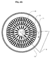
- Fig. 3 is a cross section of a portion of the turn-off power semiconductor device along the line AA' in Fig. 4A , which is a top view of the turn-off power semiconductor device shown in Fig. 3 .
- the turn-off power semiconductor device is a reverse-conducting IGCT (RC-IGCT) 100 similar to the RC-IGCT 1 known from the prior art as shown in Figures 1 and 2 .
- the RC-IGCT 100 according to the first embodiment comprises a plurality of thyristor cells 2 and an integrated free-wheeling diode 3. All thyristor cells 2 and the integrated free-wheeling diode 3 are formed in one single wafer 10 having a first main side 11 and a second main side 12.
- each thyristor cell 2 has a gate electrode 20 which is arranged on the first main side 11 of the wafer 10 lateral to the cathode semiconductor layer portion 22 and contacting the base semiconductor layer 23, but separated from the first cathode electrode 21 and the cathode semiconductor layer portion 22.
- lateral relates to the position in a lateral direction which is a direction parallel to the first main side 11.
- the free-wheeling diode 3 comprises from the first main side 11 to the second main side 12 of the wafer 10 a second anode electrode 31, a p-doped second anode semiconductor layer 32, a n + -doped second cathode semiconductor layer 33, which is separated from the p-doped second anode semiconductor layer 32 by the n - -doped drift semiconductor layer 24, and a second cathode electrode 34.
- Fig. 4A shows a top view onto the first main side 11 of the wafer 10
- Fig. 4B shows an enlarged view of the portion B of the top view shown in Fig. 4A .
- the cathode semiconductor layer portions 22 of the RC-IGCT 100 are formed in the shape of strips with its longitudinal direction aligned in radial direction, which is a direction extending from the center of the device and parallel to the first main side 11 of the wafer 10.
- the center of the device is the center of the circular wafer 10.
- strips shall be understood as layers, which have in one direction, which is their longitudinal direction, a longer extension than in the other directions by having two longer sides, which are typically arranged parallel to each other.
- the plurality of strip-shaped cathode semiconductor layer portions 22 are arranged in concentric rings 221, 222 and 223 around the center of the device.
- the surface of the base layer between the inner edges of gate electrodes 20 and the outer edges of the strip-shaped cathode semiconductor layer portions 22 is covered by a passivation oxide layer 110 to define the distance between the gate electrode 20 and the first cathode semiconductor layer portion 22 of each thyristor cell 2.
- the interface areas of the gate electrodes 20 and the base semiconductor layer 23 are defined by openings in the passivation oxide layer 110.
- the interface areas of the first cathode electrodes 21 and the corresponding cathode semiconductor layer portions 22 are defined by openings in the passivation oxide layer 110.
- passivation oxide layer 110 allows a very precise definition of the position and shape of the interface area between the gate electrode 20 and the base semiconductor layer 23 to allow for a very precise definition of the distance d 1 , d 2 and d 3 between the gate electrodes 20 and the cathode semiconductor layer portions 22.
- the layout of the thyristor cell 2 regarding the distance d 1 , d 2 , d 3 between the gate electrode 20 and the cathode semiconductor layer portion 22 and regarding the length of the strip l 1 , l 2 , l 3 is the same for all thyristor cells 2 of the respective single ring 221, 222, 223.
- the cathode semiconductor layer portions 22 of the plurality of thyristor cells 2 in a ring are arranged on the first main side 11 with rotational symmetry around the center of the device. The rotational symmetry allows a uniform distribution of the main current and of the gate current in different circular sectors of the circular wafer 10.
- a gate current pulse is supplied through the common gate contact to the gate electrodes 20 of the plurality of thyristor cells 2 to turn-off the main current flowing in the conducting state of the RC-IGCT 100 through the plurality of thyristor cells 2 from the first anode electrode 27 to the first cathode electrode 21. Due to the ohmic resistance of the gate metallization layer constituting the common gate contact 40, the gate electrodes 20 and the connections there between, a voltage drop occurs across the gate metallization layer which is increasing with increasing distance from the common gate contact 40.
- the total ohmic resistance which determines the current density of the gate current is the sum of the ohmic resistance of the gate metallization layer and the serial resistance of the base semiconductor layer 23 through which the gate current flows in a lateral direction parallel to the first main surface 11 towards the portions of the thyristor cells 2 carrying the main current in a direction vertical to the first main surface.
- the decreasing distance of the gate electrodes 20 to the cathodes semiconductor layer portions 22 decreasing with increasing distance from the common gate contact 40 has the effect that the before mentioned serial resistance of the base semiconductor layer 23 is decreasing with increasing distance from the common gate contact 40 to compensate the voltage drop which is increasing with increasing distance from the common gate contact 40.
- Fig. 5 shows a second embodiment of the turn-off power semiconductor device of the invention.
- the layout and arrangement of the gate electrodes 20 and the cathode semiconductor layer portions 22 on the first main side 11 of the wafer as described above for the first embodiment is applied to a RB-IGCT 300 (reverse blocking IGCT) as shown in Fig. 5 in cross section.
- the RB-IGCT 300 is another type of turn-off semiconductor power device which comprises a plurality of thyristor cells 302 like the RC-IGCT 100 according to the first embodiment.
- the RB-IGCT 300 differs from the RC-IGCT 100 according to the first embodiment in a different doping profile of the thyristor cells 302 across the wafer 310.
- the RB-IGCT does not comprise the buffer semiconductor layer between the drift semiconductor layer 324 and the anode semiconductor layer 326. Further, in the wafer 310 of the RB-IGCT 300 there is not integrated a free-wheeling diode.
- Each thyristor cell of the RB-IGCT 300 shown in Fig. 5 comprises from the first main side 11 of the wafer 310 to the second main side 12 of the wafer 310 a first cathode electrode 21, a n + -doped cathode semiconductor layer portion 22, a p-doped base semiconductor layer 323, a n-doped drift semiconductor layer 324, a p + -doped anode semiconductor layer 326 and an first anode electrode 27.
- the cathode semiconductor layer portions 22 of the plurality of thyristor cells 302 form a first cathode semiconductor layer.
- the different doping profiles of the thyristor cells 2 of the RC-IGCT 100 and of the thyristor cells 302 of the RB-IGCT 300 are due to optimization for different device characteristics.
- a smooth transition from the forward conductive state to the reverse blocking state (soft reverse recovery) is desired.
- the drift semiconductor layer 324 of a RB-IGCT has to be thicker than that of an optimized RC-IGCT.
- the carrier life time in the drift semiconductor layer 324 of the RB-IGCT has to be adapted by introducing low lifetime areas in regions of the drift semiconductor layer 324 near the base semiconductor layer 323 and the anode semiconductor layer 326. This can be done by proton implantation.
- the arrangement and layout of the RB-IGCT 300 with regard to the common gate contact 40, the gate electrodes 20 and the cathode semiconductor layer portions 22 on the first main side 11 of the wafer 310 is the same as in the RC-IGCT 100 as described above with reference to Figures 4A and 4B . Accordingly, the same effects with regard to uniformity of the gate current density and turn-off performance can be achieved.
- the GTO does not comprise the buffer semiconductor layer between the drift semiconductor layer 424 and the first anode semiconductor layer 426.
- the wafer 410 of the GTO 400 there is not integrated a free-wheeling diode.
- the different doping profiles of the thyristor cells 2 of the RC-IGCT 100 and of the thyristor cells 402 of the GTO 400 is mainly due to optimization for a different gate control.
- the full load main current is commutated from the cathode to the gate within a few micro-seconds during turn-off, whereas the GTO 400 is turned off with a gate current pulse of much lower gate current density.
- Each thyristor cell of the GTO 400 shown in Fig. 6 comprises from the first main side 11 of the wafer 410 to the second main side 12 of the wafer 410 a cathode electrode 21, a n + -doped cathode semiconductor layer portion 22, a p-doped base semiconductor layer 423, a n-doped drift semiconductor layer 424, a p + -doped anode semiconductor layer 426 and an anode electrode 27.
- the cathode semiconductor layer portions 22 of the plurality of thyristor cells 402 form a first cathode semiconductor layer.
- each thyristor cell 402 of the GTO 400 has a gate electrode 20 which is arranged on the first main side 11 of the wafer 410 lateral to the cathode semiconductor layer portion 22 and contacting the base semiconductor layer 23, but separated from the first cathode electrode 21 and the cathode semiconductor layer portion 22.
- the term "lateral" relates to the position in a lateral direction which is a direction parallel to the first main side 11.
- the arrangement and layout of the GTO 400 with regard to the common gate contact 40, the gate electrodes 20 and the cathode semiconductor layer portions 22 on the first main side 11 of the wafer 410 is the same as in the RC-IGCT 100 as described above with reference to Figures 4A and 4B . Accordingly, the same effects with regard to uniformity of the gate current density and turn-off performance can be achieved.
- Fig. 7 there is illustrated a modification of the gate turn-off power semiconductor devices according to the first to third embodiment, respectively.
- Fig. 7 shows an enlarged view of the layout of thyristor cells of three different rings in top view. It shows the cathode semiconductor layer portions 22 surrounded by gate electrodes 20.
- This modified embodiment differs from the first to third embodiment only in that the distance between the gate electrode 20 and the cathode semiconductor layer portion 22 of one single thyristor cell is not constant anymore along the circumferential edge of the cathode semiconductor layer portion 22. Rather, the distance between the gate electrode 20 and the cathode semiconductor layer portion 22 of one single thyristor cell decreases along the longitudinal axis of the strip-shaped cathode semiconductor portion 22 with increasing distance r from the common gate contact 40.
- Fig. 7 there is also shown a graph of the distance between the gate electrode 20 and the cathode semiconductor layer portion 22 as a function of the distance r from the common gate contact 40.
- the distance d 1 between the gate electrode 20 and the cathode semiconductor layer portion 22 is decreasing along the longitudinal axis of the cathode semiconductor layer portion 22 with increasing distance r from the common gate contact 40 from a maximum distance d 1,max to a minimum distance d 1,min .
- the distance d 2 between the gate electrode 20 and the cathode semiconductor layer portion 22 is decreasing along the longitudinal axis of the cathode semiconductor layer portion 22 with increasing distance r from the common gate contact 40 from a maximum distance d 2,max to a minimum distance d 2,min , wherein the maximum distance d 2,max is equal to the minimum distance d 1,min in the thyristor cells of the first ring.
- the distance d 3 between the gate electrode 20 and the cathode semiconductor layer portion 22 is decreasing along the longitudinal axis of the cathode semiconductor layer portion 22 with increasing distance r from the common gate contact 40 from a maximum distance d 3,max to a minimum distance d 3,min , wherein the maximum distance d 3,max is equal to the minimum distance d 2,min in the thyristor cells of the second ring.
- Fig. 7 shows only one thyristor cell of each one of the first to third ring
- the layout of the remaining thyristor cells regarding the distance d 1 , d 2 , d 3 between the gate electrode 20 and the cathode semiconductor layer portion 22 and regarding the length of the strip l 1 , l 2 , l 3 is the same for all remaining thyristor cells of these rings, respectively.
- the thyristor cells could include a p + -doped cathode semiconductor layer portion, a n-doped base semiconductor layer, a p-doped drift semiconductor layer, a p + -doped buffer semiconductor layer and a n-doped first anode semiconductor layer.
Landscapes
- Thyristors (AREA)
Abstract
The invention relates to a turn-off power semiconductor device (100) comprising a plurality of thyristor cells (2). In the turn-off power semiconductor device (100) of the invention, the distance between a gate electrode (20) and a cathode semiconductor layer portion (22) depends on the distance of the thyristor cell (2) from a common gate contact (40). Specifically, for each pair of a first thyristor cell and a second thyristor cell of the plurality of thyristor cells (2), for which the distance between the first thyristor cell and the common gate contact (40) is smaller than the distance between the second thyristor cell and the common gate contact (40), a minimum distance between the gate electrode (20) and the cathode semiconductor layer portion (22) is smaller in the second thyristor cell than in the first thyristor cell.
Description
- The invention relates to the field of power semiconductor devices and in particular to a turn-off power semiconductor device according to the preamble of
claim 1. - In the field of power semiconductor devices there are known turn-off power semiconductor devices such as a gate turn-off thyristor (GTO), and a gate commutated thyristor (GCT), in particular an integrated gate commutated thyristor (IGCT). There is known a reverse blocking IGCT (RB-IGCT) and a reverse-conducting IGCT (RC-IGCT).
- As an example for a known turn-off power semiconductor device a prior art RC-IGCT 1 is shown in
Figures 1 and2 . Such RC-IGCT is described for example inWO 2012/041958 A2 .Fig. 1 illustrates a portion of the known RC-IGCT 1 in cross section andFig. 2 shows the layout of the device in top view. The RC-IGCT 1 comprises a plurality ofthyristor cells 2 and an integrated free-wheeling diode 3. Allthyristor cells 2 and the integrated free-wheeling diode 3 are formed in onesingle wafer 10 having a firstmain side 11, which is the cathode side of the RC-IGCT 1, and a secondmain side 12, which is the anode side of the RC-IGCT 1. - As can be seen in
Fig. 1 , eachthyristor cell 2 comprises from the firstmain side 11 to the secondmain side 12 of the wafer 10 afirst cathode electrode 21, a n+-doped cathodesemiconductor layer portion 22, a p-dopedbase semiconductor layer 23, a n--dopeddrift semiconductor layer 24, abuffer semiconductor layer 25, a p+-doped firstanode semiconductor layer 26 and afirst anode electrode 27. The cathodesemiconductor layer portions 22 of the plurality ofthyristor cells 2 form a first cathode semiconductor layer. Therein thebuffer semiconductor layer 25 has a rising doping concentration towards the secondmain side 12, whereas the drift semiconductor layer has typically a constant doping concentration. - Further, each
thyristor cell 2 has agate electrode 20 which is arranged on the firstmain side 11 of thewafer 10 lateral to the cathodesemiconductor layer portion 22 and contacting thebase semiconductor layer 23, but separated from thefirst cathode electrode 21 and the cathodesemiconductor layer portion 22. Therein, the term "lateral" relates to the position in a lateral direction which is a direction parallel to the firstmain side 11. - In the circumferential edge region of the
wafer 10 there is arranged the integrated single free-wheeling diode 3, a cross section of which along the line AA' inFig. 2 can also be seen inFig. 1 . The free-wheeling diode 3 comprises from the firstmain side 11 to the secondmain side 12 of the wafer 10 asecond anode electrode 31, a p-doped secondanode semiconductor layer 32, a n+-doped secondcathode semiconductor layer 33, which is separated from the p-doped secondanode semiconductor layer 32 by the n--dopeddrift semiconductor layer 24, and asecond cathode electrode 34. - The arrangement of the plurality of
thyristor cells 2 in the RC-IGCT 1 is illustrated inFig. 2 which shows a top view onto the firstmain side 11 of the wafer. The cathodesemiconductor layer portions 22 of the RC-IGCT 1 are formed in the shape of strips with its longitudinal direction aligned in radial direction which is a direction extending from the center of the device and being parallel to the firstmain side 11 of thewafer 10. Therein, the center of the device is the center of the first main side of thecircular wafer 10. Further, strips shall be understood as layers, which have in one direction, which is their longitudinal direction, a longer extension than in the other directions by having two longer sides, which are typically arranged parallel to each other. The plurality of strip-shaped cathodesemiconductor layer portions 22 are arranged in concentric rings around the center of the device. In the center region of thewafer 10 there is arranged acommon gate contact 40 to which allgate electrodes 20 of the plurality ofthyristor cells 2 are electrically connected. Thegate electrodes 20 of thethyristor cells 2, thecommon gate contact 40 and the connections there between are implemented as a gate metallization layer surrounding all the cathodesemiconductor layer portions 22. - For turning off the RC-IGCT, a short control gate current pulse is supplied through the
common gate contact 40 to thegate electrodes 20 of the plurality ofthyristor cells 2. The uniformity of the current distribution to the plurality ofthyristor cells 2 is an important parameter for the turn-off performance of the RC-IGCT 1. In the RG-IGCT described above withFigures 1 and2 , thecommon gate contact 40 is located on the firstmain side 11 in the center thereof. Thethyristor cells 2 in an outer ring are turned off by a lower gate current than thyristor cells of an inner ring. Therefore the charge under the cathode semiconductor layer portions of an inner ring is removed faster than that under the cathode semiconductor layer portions of an outer ring. Accordingly, the thyristor cells of an outer ring remain in an on-state longer and consequently can be overheated what may finally result in destruction of the whole device. - The same problem of non-uniform turn-off of thyristor cells due to an inhomogeneous gate current distribution exists not only for the RC-IGCT but also for any other turn-off semiconductor power device comprising a plurality of thyristor cells.
- To homogenize the current distribution it is known a turn-off power semiconductor device where the common gate contact has the shape of a concentric ring located on the first main side at the perimeter of the wafer. In another turn-off power semiconductor device as described in
EP 0 592 991 A1 , the common gate contact is located between two rings of thyristor cells somewhere between the center and the perimeter of the device. This known approaches have, however, the disadvantage that they can only alleviate the local inhomogeneities of the gate current pulse to the plurality of thyristor cells but cannot avoid them. Further, the ring-shaped common gate contact consumes more of the active area of the device than devices with a central common gate contact. Finally, also housing of devices with a ring shaped common gate contact is more complicated and involves higher costs compared to housing a device with central common gate contact. - It is the object of the invention improve the turn-off performance of a turn-off power semiconductor device having a plurality of thyristor cells by decreasing the inhomogeneities of the gate current density in the turn-off power semiconductor device.
- The object of the invention is attained by a turn-off power semiconductor device according to
claim 1. - In the turn-off power semiconductor device of the invention the distance between the gate electrode and the cathode semiconductor layer portion depends on the distance of the thyristor cell from the common gate contact. Specifically, for each pair of a first thyristor cell and a second thyristor cell of the plurality of thyristor cells, for which the distance between the first thyristor cell and the common gate contact is smaller than the distance between the second thyristor cell and the common gate contact, a minimum distance between the gate electrode and the cathode semiconductor layer portion is smaller in the second thyristor cell than in the first thyristor cell.
- The decreasing distance between gate electrode and the cathode semiconductor layer portion in a thyrisor cell with increasing distance of the thyristor cells from the common gate contact results in a decreasing serial resistance of the base semiconductor layer connecting the gate electrode to the cathode semiconductor layer portion. In this way the decreased distance between the gate electrode and the cathode semiconductor layer portion with increasing distance of the thyristor cells from the common gate contact can compensate the increasing voltage drop with increasing distance from the common gate contact.
- As a result, the inhomogeneities of the gate current density in the device can be avoided and the thyristor cells can be turned off at the same time to improve the turn-off performance of the turn-off power semiconductor device accordingly.
- Further developments of the invention are specified in the dependent claims.
- In an exemplary embodiment of the turn-off power semiconductor device, the common gate contact is arranged in the center of the device on the first main side. Compared to other designs where the main gate contact is formed as a ring either at the perimeter of the wafer or somewhere between the center and the perimeter of the wafer, the design with the main contact arranged in the center of the device consumes less active area of the device. Further, housing the device with the common gate contact in the center is less complicated and, therefore, costs for housing are lower compared to the costs for housing of devices with a ring shaped common gate contact.
- In a preferred embodiment of the turn-off power semiconductor device, the cathode semiconductor layer portions of the plurality of thyristor cells are arranged with rotational symmetry around the center of the device on the first main side. In such arrangement with rotational symmetry, the main current distribution and the gate current distribution have also a rotational symmetry and can be made more uniform.
- In an exemplary embodiment of the turn-off power semiconductor device the cathode semiconductor layer portions of the plurality of thyristor cells are formed on the first main side as strips placed in concentric rings around the center of the device, the longitudinal axis of each strip extending along a radial direction which is a direction extending from the center of the device in a plane parallel to the first main side. Such arrangement can improve the uniformity of the main current through the device and minimize the voltage drop of the electrical connection between common gate contact and gate electrodes along the radial direction extending from the center of the device. Moreover, such arrangement can optimize the usage of the active area of the device.
- In one exemplary embodiment the distance between the gate electrode and the cathode semiconductor layer portion is decreasing along the longitudinal axis of the strip-shaped cathode semiconductor layer portions with increasing distance from the common gate contact in each one of the plurality of thyristor cells. In this way a voltage drop in the gate electrode along the longitudinal axis of each single thyristor cell can be efficiently compensated.
- In a preferred embodiment the distance between the gate electrode and the cathode semiconductor layer portion is constant along the longitudinal axis in each one of the plurality of thyristor cells, respectively. Such layout with a single constant distance for each thyristor cell is more easy to produce and decreases the costs for manufacturing the device, whereas the gate current distribution in the different thyristor cells is approximately equalised due to the decreasing distances of the gate electrode from the cathode semiconductor layer portion for thyristor cells with increasing distance to the common gate contact.
- In a preferred embodiment the base semiconductor layer between the cathode semiconductor layer portion and the gate electrode of each thyristor cell is covered by a passivation oxide layer to define the distance between the gate electrode and the first cathode semiconductor layer of each thyristor cell. With such structure, the distance between the gate electrode and the cathode semiconductor layer portion can be defined precisely.
- Detailed embodiments of the invention will be explained below with reference to the accompanying figures, in which
-
Fig. 1 is a cross section of a portion of a turn-off power semiconductor device known from the prior art along a line AA' inFig. 2 ; -
Fig. 2 is top view of the turn-off power semiconductor device shown inFig. 1 ; -
Fig. 3 is a cross section of a portion of a turn-off power semiconductor device according to a first embodiment; -
Fig. 4A is top view of the turn-off power semiconductor device shown inFig. 3 ; -
Fig. 4B is an enlarged view of a portion of the top view shown inFig. 4A ; -
Fig. 5 is a cross section of a turn-off power semiconductor device according to a second embodiment; -
Fig. 6 is a cross section of a turn-off power semiconductor device according to a third embodiment; and -
Fig. 7 is a an enlarged top view of a portion of a turn-off power semiconductor device according to a fourth embodiment and a graph which shows the distance between the gate electrode and the cathode semiconductor layer portion as a function of the distance r from the common gate electrode. - The reference signs used in the figures and their meanings are summarized in the list of reference signs. Generally, similar elements have the same reference signs throughout the specification. The described embodiments are meant as examples and shall not limit the scope of the invention.
-
Figures 3 and4 show a turn-off power semiconductor device according to a first embodiment.Fig. 3 is a cross section of a portion of the turn-off power semiconductor device along the line AA' inFig. 4A , which is a top view of the turn-off power semiconductor device shown inFig. 3 . - The turn-off power semiconductor device according to the first embodiment is a reverse-conducting IGCT (RC-IGCT) 100 similar to the RC-
IGCT 1 known from the prior art as shown inFigures 1 and2 . The RC-IGCT 100 according to the first embodiment comprises a plurality ofthyristor cells 2 and an integrated free-wheelingdiode 3. Allthyristor cells 2 and the integrated free-wheelingdiode 3 are formed in onesingle wafer 10 having a firstmain side 11 and a secondmain side 12. - As can be seen in
Fig. 3 , eachthyristor cell 2 comprises from the firstmain side 11 to the secondmain side 12 of the wafer 10 afirst cathode electrode 21, a n+-doped cathodesemiconductor layer portion 22, a p-dopedbase semiconductor layer 23, a n--dopeddrift semiconductor layer 24, abuffer semiconductor layer 25, a p+-doped firstanode semiconductor layer 26 and afirst anode electrode 27. The cathodesemiconductor layer portions 22 of the plurality ofthyristor cells 2 form a first cathode semiconductor layer. Therein thebuffer semiconductor layer 25 has a rising doping concentration towards the secondmain side 12, whereas thedrift semiconductor layer 24 has approximately a constant low doping concentration. - Further, each
thyristor cell 2 has agate electrode 20 which is arranged on the firstmain side 11 of thewafer 10 lateral to the cathodesemiconductor layer portion 22 and contacting thebase semiconductor layer 23, but separated from thefirst cathode electrode 21 and the cathodesemiconductor layer portion 22. Therein, the term "lateral" relates to the position in a lateral direction which is a direction parallel to the firstmain side 11. - In the circumferential edge region of the
wafer 10 there is arranged the integrated single free-wheelingdiode 3, a cross section of which along the line AA' inFig. 4A can also be seen inFig. 3 . The free-wheelingdiode 3 comprises from the firstmain side 11 to the secondmain side 12 of the wafer 10 asecond anode electrode 31, a p-doped secondanode semiconductor layer 32, a n+-doped secondcathode semiconductor layer 33, which is separated from the p-doped secondanode semiconductor layer 32 by the n--dopeddrift semiconductor layer 24, and asecond cathode electrode 34. - The arrangement of the plurality of
thyristor cells 2 in the RC-IGCT 100 can be seen inFig. 4A , which shows a top view onto the firstmain side 11 of thewafer 10, and inFig. 4B , which shows an enlarged view of the portion B of the top view shown inFig. 4A . - As in the RC-
IGCT 1 shown inFigures 1 and2 , the cathodesemiconductor layer portions 22 of the RC-IGCT 100 are formed in the shape of strips with its longitudinal direction aligned in radial direction, which is a direction extending from the center of the device and parallel to the firstmain side 11 of thewafer 10. As above in the description of the prior art, the center of the device is the center of thecircular wafer 10. Further, strips shall be understood as layers, which have in one direction, which is their longitudinal direction, a longer extension than in the other directions by having two longer sides, which are typically arranged parallel to each other. The plurality of strip-shaped cathodesemiconductor layer portions 22 are arranged inconcentric rings wafer 10 there is arranged acommon gate contact 40 to which allgate electrodes 20 of the plurality ofthyristor cells 2 are electrically connected. Thegate electrodes 20 of thethyristor cells 2, thecommon gate contact 40 and the connections there between are implemented as a gate metallization layer surrounding all the cathodesemiconductor layer portions 22. - Also, the upper side of the gate metallization layer is on a level lower than the upper side of the
cathode electrodes 21 of the plurality ofthyristor cells 2 when the firstmain side 11 forms an upper side of the device and the secondmain side 12 forms a lower side of the device. - In the RC-
IGCT 100 according to the first embodiment all cathodesemiconductor layer portions 22 in the innermostfirst ring 221 have the same length l1 along its longitudinal axis, whereas all cathodesemiconductor layer portions 22 in thesecond ring 222 have the same length l2 along its longitudinal axis which is longer than l1 (i.e. l1 < l2). Likewise, all cathodesemiconductor layer portions 22 in the outermostthird ring 223 have the same length l3 along its longitudinal axis which is longer than l2 (i.e. l2 < l3). The increasing length from the center toward the circumferential edge of the wafer allows an efficient use of the active area of the wafer. - Throughout the specification, the distance between the
gate electrode 20 and the cathodesemiconductor layer portion 22 shall be the distance in a lateral direction parallel to the firstmain side 11 between an edge of an interface area of thegate electrode 20 with thebase semiconductor layer 23 and an edge of an interface area of the cathodesemiconductor layer portion 22 with thebase semiconductor layer 23. In other words, the distance between thegate electrode 20 and the cathodesemiconductor layer portion 22 is a distance between the interface area of thegate electrode 20 with thebase semiconductor layer 23 and an edge of an interface area of the cathodesemiconductor layer portion 22 with thebase semiconductor layer 23 in an orthogonal projection onto a plane parallel to the firstmain side 11 of thewafer 10. - Referring to
Fig. 3 , the surface of the base layer between the inner edges ofgate electrodes 20 and the outer edges of the strip-shaped cathodesemiconductor layer portions 22 is covered by apassivation oxide layer 110 to define the distance between thegate electrode 20 and the first cathodesemiconductor layer portion 22 of eachthyristor cell 2. The interface areas of thegate electrodes 20 and thebase semiconductor layer 23 are defined by openings in thepassivation oxide layer 110. Likewise, also the interface areas of thefirst cathode electrodes 21 and the corresponding cathodesemiconductor layer portions 22 are defined by openings in thepassivation oxide layer 110. The use of thepassivation oxide layer 110 allows a very precise definition of the position and shape of the interface area between thegate electrode 20 and thebase semiconductor layer 23 to allow for a very precise definition of the distance d1, d2 and d3 between thegate electrodes 20 and the cathodesemiconductor layer portions 22. - As shown in
Fig. 4B , the distance d1 between thegate electrode 20 and the cathodesemiconductor layer portion 22 of each thyristor cell in thefirst ring 221 is constant along the whole circumferential edge of the cathodesemiconductor layer portion 22. Likewise, the distance d2 between thegate electrode 20 and the cathodesemiconductor layer portion 22 of each thyristor cell in thesecond ring 222 is constant along the whole circumferential edge of the cathodesemiconductor layer portion 22 and the distance d3 between thegate electrode 20 and the cathodesemiconductor layer portion 22 of each thyristor cell in thethird ring 223 is constant along the whole circumferential edge of the cathodesemiconductor layer portion 22. Therein, the distance between thegate electrode 20 and the cathodesemiconductor layer portion 22 decreases from ring to ring with increasing distance from the common gate contact 40 (i.e. d1 > d2 > d3). - Accordingly, for each single ring of the
rings Fig. 4B , the layout of thethyristor cell 2 regarding the distance d1, d2, d3 between thegate electrode 20 and the cathodesemiconductor layer portion 22 and regarding the length of the strip l1, l2, l3 is the same for allthyristor cells 2 of the respectivesingle ring semiconductor layer portions 22 of the plurality ofthyristor cells 2 in a ring are arranged on the firstmain side 11 with rotational symmetry around the center of the device. The rotational symmetry allows a uniform distribution of the main current and of the gate current in different circular sectors of thecircular wafer 10. - In operation of the RC-
IGCT 100, a gate current pulse is supplied through the common gate contact to thegate electrodes 20 of the plurality ofthyristor cells 2 to turn-off the main current flowing in the conducting state of the RC-IGCT 100 through the plurality ofthyristor cells 2 from thefirst anode electrode 27 to thefirst cathode electrode 21. Due to the ohmic resistance of the gate metallization layer constituting thecommon gate contact 40, thegate electrodes 20 and the connections there between, a voltage drop occurs across the gate metallization layer which is increasing with increasing distance from thecommon gate contact 40. The total ohmic resistance which determines the current density of the gate current is the sum of the ohmic resistance of the gate metallization layer and the serial resistance of thebase semiconductor layer 23 through which the gate current flows in a lateral direction parallel to the firstmain surface 11 towards the portions of thethyristor cells 2 carrying the main current in a direction vertical to the first main surface. The decreasing distance of thegate electrodes 20 to the cathodessemiconductor layer portions 22 decreasing with increasing distance from thecommon gate contact 40 has the effect that the before mentioned serial resistance of thebase semiconductor layer 23 is decreasing with increasing distance from thecommon gate contact 40 to compensate the voltage drop which is increasing with increasing distance from thecommon gate contact 40. Thereby, the current density of the gate current flowing in eachthyristor cell 2 can be made the same independent from the distance of thethyristor cell 2 from thecommon gate contact 40. A uniform current density of the gate current for all thyristor cells results in a simultaneous turn-off of all the thyristor cells. Accordingly, the turn-off performance is improved in the RC-IGCT 100 according to the first embodiment. -
Fig. 5 shows a second embodiment of the turn-off power semiconductor device of the invention. In this second embodiment, the layout and arrangement of thegate electrodes 20 and the cathodesemiconductor layer portions 22 on the firstmain side 11 of the wafer as described above for the first embodiment is applied to a RB-IGCT 300 (reverse blocking IGCT) as shown inFig. 5 in cross section. The RB-IGCT 300 is another type of turn-off semiconductor power device which comprises a plurality ofthyristor cells 302 like the RC-IGCT 100 according to the first embodiment. The RB-IGCT 300 differs from the RC-IGCT 100 according to the first embodiment in a different doping profile of thethyristor cells 302 across thewafer 310. In particular, the RB-IGCT does not comprise the buffer semiconductor layer between thedrift semiconductor layer 324 and theanode semiconductor layer 326. Further, in thewafer 310 of the RB-IGCT 300 there is not integrated a free-wheeling diode. - Each thyristor cell of the RB-
IGCT 300 shown inFig. 5 comprises from the firstmain side 11 of thewafer 310 to the secondmain side 12 of the wafer 310 afirst cathode electrode 21, a n+-doped cathodesemiconductor layer portion 22, a p-dopedbase semiconductor layer 323, a n-dopeddrift semiconductor layer 324, a p+-dopedanode semiconductor layer 326 and anfirst anode electrode 27. The cathodesemiconductor layer portions 22 of the plurality ofthyristor cells 302 form a first cathode semiconductor layer. - The different doping profiles of the
thyristor cells 2 of the RC-IGCT 100 and of thethyristor cells 302 of the RB-IGCT 300 are due to optimization for different device characteristics. In the RB-IGCT 300 a smooth transition from the forward conductive state to the reverse blocking state (soft reverse recovery) is desired. As a result, thedrift semiconductor layer 324 of a RB-IGCT has to be thicker than that of an optimized RC-IGCT. Also the carrier life time in thedrift semiconductor layer 324 of the RB-IGCT has to be adapted by introducing low lifetime areas in regions of thedrift semiconductor layer 324 near thebase semiconductor layer 323 and theanode semiconductor layer 326. This can be done by proton implantation. - Like the
thyristor cells 2 of the RC-IGCT 100 according to the first embodiment, eachthyristor cell 302 of the RB-IGCT 300 has agate electrode 20 which is arranged on the firstmain side 11 of thewafer 310 lateral to the cathodesemiconductor layer portion 22 and contacting thebase semiconductor layer 323, but separated from thecathode electrode 21 and the cathodesemiconductor layer portion 22. Therein, the term "lateral" relates to the position in a lateral direction which is a direction parallel to the firstmain side 11. - The arrangement and layout of the RB-
IGCT 300 with regard to thecommon gate contact 40, thegate electrodes 20 and the cathodesemiconductor layer portions 22 on the firstmain side 11 of thewafer 310 is the same as in the RC-IGCT 100 as described above with reference toFigures 4A and4B . Accordingly, the same effects with regard to uniformity of the gate current density and turn-off performance can be achieved. -
Fig. 6 shows a third embodiment of the turn-off power semiconductor device of the invention. In this third embodiment, the arrangement and layout of thegate electrodes 20 and the cathodesemiconductor layer portions 22 on the firstmain side 11 of the wafer as described above for the first embodiment is applied to a GTO (gate turn-off thyristor) 400 as shown inFig. 6 in cross section. TheGTO 400 is another type of turn-off semiconductor power device which comprises, like the RC-IGCT 100 according to the first embodiment, a plurality ofthyristor cells 402. TheGTO 400 differs from the RC-IGCT 100 according to the first embodiment in a different doping profile of thethyristor cells 402 across thewafer 410. In particular, the GTO does not comprise the buffer semiconductor layer between thedrift semiconductor layer 424 and the firstanode semiconductor layer 426. Further, in thewafer 410 of theGTO 400 there is not integrated a free-wheeling diode. The different doping profiles of thethyristor cells 2 of the RC-IGCT 100 and of thethyristor cells 402 of theGTO 400 is mainly due to optimization for a different gate control. In the IGCT the full load main current is commutated from the cathode to the gate within a few micro-seconds during turn-off, whereas theGTO 400 is turned off with a gate current pulse of much lower gate current density. - Each thyristor cell of the
GTO 400 shown inFig. 6 comprises from the firstmain side 11 of thewafer 410 to the secondmain side 12 of the wafer 410 acathode electrode 21, a n+-doped cathodesemiconductor layer portion 22, a p-dopedbase semiconductor layer 423, a n-dopeddrift semiconductor layer 424, a p+-dopedanode semiconductor layer 426 and ananode electrode 27. In addition there are disposed a plurality of n+-doped anodeshort semiconductor regions 450 between the n-dopeddrift semiconductor layer 424 and theanode electrode 27 in the p+-dopedanode semiconductor layer 426. The cathodesemiconductor layer portions 22 of the plurality ofthyristor cells 402 form a first cathode semiconductor layer. - Further, like the
thyristor cells 2 of the RC-IGCT 100 according to the first embodiment, eachthyristor cell 402 of theGTO 400 has agate electrode 20 which is arranged on the firstmain side 11 of thewafer 410 lateral to the cathodesemiconductor layer portion 22 and contacting thebase semiconductor layer 23, but separated from thefirst cathode electrode 21 and the cathodesemiconductor layer portion 22. Therein, the term "lateral" relates to the position in a lateral direction which is a direction parallel to the firstmain side 11. - The arrangement and layout of the
GTO 400 with regard to thecommon gate contact 40, thegate electrodes 20 and the cathodesemiconductor layer portions 22 on the firstmain side 11 of thewafer 410 is the same as in the RC-IGCT 100 as described above with reference toFigures 4A and4B . Accordingly, the same effects with regard to uniformity of the gate current density and turn-off performance can be achieved. - In
Fig. 7 there is illustrated a modification of the gate turn-off power semiconductor devices according to the first to third embodiment, respectively.Fig. 7 shows an enlarged view of the layout of thyristor cells of three different rings in top view. It shows the cathodesemiconductor layer portions 22 surrounded bygate electrodes 20. This modified embodiment differs from the first to third embodiment only in that the distance between thegate electrode 20 and the cathodesemiconductor layer portion 22 of one single thyristor cell is not constant anymore along the circumferential edge of the cathodesemiconductor layer portion 22. Rather, the distance between thegate electrode 20 and the cathodesemiconductor layer portion 22 of one single thyristor cell decreases along the longitudinal axis of the strip-shapedcathode semiconductor portion 22 with increasing distance r from thecommon gate contact 40. - In
Fig. 7 there is also shown a graph of the distance between thegate electrode 20 and the cathodesemiconductor layer portion 22 as a function of the distance r from thecommon gate contact 40. As shown inFig. 7 , in a thyristor cell of thefirst ring 221 the distance d1 between thegate electrode 20 and the cathodesemiconductor layer portion 22 is decreasing along the longitudinal axis of the cathodesemiconductor layer portion 22 with increasing distance r from thecommon gate contact 40 from a maximum distance d1,max to a minimum distance d1,min. In a thyristor cell of thesecond ring 222, the distance d2 between thegate electrode 20 and the cathodesemiconductor layer portion 22 is decreasing along the longitudinal axis of the cathodesemiconductor layer portion 22 with increasing distance r from thecommon gate contact 40 from a maximum distance d2,max to a minimum distance d2,min, wherein the maximum distance d2,max is equal to the minimum distance d1,min in the thyristor cells of the first ring. In a thyristor cell of thethird ring 223, the distance d3 between thegate electrode 20 and the cathodesemiconductor layer portion 22 is decreasing along the longitudinal axis of the cathodesemiconductor layer portion 22 with increasing distance r from thecommon gate contact 40 from a maximum distance d3,max to a minimum distance d3,min, wherein the maximum distance d3,max is equal to the minimum distance d2,min in the thyristor cells of the second ring. - While
Fig. 7 shows only one thyristor cell of each one of the first to third ring, the layout of the remaining thyristor cells regarding the distance d1, d2, d3 between thegate electrode 20 and the cathodesemiconductor layer portion 22 and regarding the length of the strip l1, l2, l3 is the same for all remaining thyristor cells of these rings, respectively. - Like explained in detail for the first embodiment, differences in voltage drop across the gate metallization layer can be compensated by the decreasing distance between
gate electrode 20 and cathodesemiconductor layer portion 22 with increasing distance from the common gate contact. In the embodiment there cannot only be compensated differences in the voltage drop from ring to ring but also along the longitudinal axis of each single cathodesemiconductor layer portion 22. - Further modifications of the above described embodiments are possible.
- In the modified embodiment described with
Fig. 7 , it was described that the maximum and minimum distances fulfil the following two equations:

- However, to compensate the voltage drop along the distance separating one ring from the next on, it is also possible that these equations are modified as follows


- Further, the embodiments were described with three rings. However, the number of rings could be any number above one.
- The above embodiments were explained with specific conductivity types. The conductivity types of the semiconductor layers in the above described embodiments might be switched, so that all layers which were described as p-type layers would be n-type layers and all layers which were described as n-type layers would be p-type layers. For example, in a modified first embodiment, the thyristor cells could include a p+-doped cathode semiconductor layer portion, a n-doped base semiconductor layer, a p-doped drift semiconductor layer, a p+-doped buffer semiconductor layer and a n-doped first anode semiconductor layer.
- All embodiments were described with a central
common gate contact 40. However, the invention is not limited to such central common gate contact. It would also be possible to have ring-shaped common gate contact at the perimeter of the wafer or even between two rings somewhere between the perimeter and the center of the wafer. - It should be noted that the term "comprising" does not exclude other elements or steps and that the indefinite article "a" or "an" does not exclude the plural. Also elements described in association with different embodiments may be combined.
-
- 1
- reverse conducting IGCT (RC-IGCT)
- 2
- thyristor cell
- 3
- integrated free-wheeling diode
- 10
- wafer
- 11
- first main side
- 12
- second main side
- 20
- gate electrode
- 21
- first cathode electrode
- 22
- cathode semiconductor layer portion
- 23
- base semiconductor layer
- 24
- drift semiconductor layer
- 25
- buffer semiconductor layer
- 26
- first anode semiconductor layer
- 27
- first anode electrode
- 31
- second anode electrode
- 32
- second anode semiconductor layer
- 33
- second cathode semiconductor layer
- 34
- second cathode electrode
- 40
- common gate contact
- 100
- reverse conducting IGCT (RC-IGCT)
- 110
- passivation oxide layer
- 221
- first ring
- 222
- second ring
- 223
- third ring
- 300
- reverse blocking IGCT (RB-IGCT)
- 302
- thyristor cell
- 310
- wafer
- 323
- base semiconductor layer
- 324
- drift semiconductor layer
- 326
- first anode semiconductor layer
- 400
- GTO (gate turn-off thyristor)
- 402
- thyristor cell
- 410
- wafer
- 423
- base semiconductor layer
- 424
- drift semiconductor layer
- 426
- first anode semiconductor layer
- 450
- anode short semiconductor region
Claims (15)
- A Turn-off power semiconductor device comprising:a wafer (10; 310; 410) having a first main side (11) and a second main side (12),which is arranged parallel to the first main side (11);a plurality ofthyristor cells (2; 302; 402) arranged between the first main side (11) and the second main side (12), each of the plurality of thyristor cells (2; 302; 402) comprising in the order from the first main side (11) to the second main side (12):(a) a first cathode electrode (21);(b) a cathode semiconductor layer portion (22) of a first conductivity type;(c) a base semiconductor layer (23; 323; 423) of a second conductivity type different from the first conductivity type;(d) a drift semiconductor layer (24; 324; 424) of the first conductivity type;(e) a first anode semiconductor layer (26; 326; 426) of the second conductivity type;(f) a first anode electrode (27),wherein each thyristor cell (2; 302; 402) further comprises a gate electrode (20) which is arranged lateral to the cathode semiconductor layer portion (22) andcontacting the base semiconductor layer (23; 323; 423),wherein the cathode semiconductor layer portions (22) of the plurality of thyristor cells (2; 302; 402) form a first cathode semiconductor layer, andwherein the gate electrodes (20) of the plurality of thyristor cells (2; 302; 402) are electrically connected with each other;the device further comprising a common gate contact (40) for contacting the gate electrodes (20) of the plurality of thyristor cells (2; 302; 402),characterized in thatfor each pair of a first thyristor cell and a second thyristor cell of the plurality of thyristor cells (2; 302; 402), for which a distance between the first thyristor cell and the common gate contact (40) is smaller than a distance between the second thyristor cell and the common gate contact (40), a minimum distance (d1,min, d2,min, d3,min) between the gate electrode (20) and the cathode semiconductor layer portion (22) is smaller in the second thyristor cell than in the first thyristor cell,wherein a distance (d1, d2, d3) between the gate electrode (20) and the cathode semiconductor layer portion (22) is the distance in a lateral direction parallel to the first main side (11) between an edge of an interface area of the gate electrode (20) with the base semiconductor layer (23; 323; 423) and an edge of an interface area of the cathode semiconductor layer portion (22) with the base semiconductor layer (23; 323; 423).
- The Turn-off power semiconductor device according to claim 1, wherein the common gate contact (40) is arranged in the center of the device on the first main side (11).
- The Turn-off power semiconductor device according to claim 1 or 2, wherein the cathode semiconductor layer portions (22) of the plurality of thyristor cells (2; 302; 402) are arranged on the first main side (11) with rotational symmetry around the center of the device.
- The Turn-off power semiconductor device according to any one of claims 1 to 3, wherein the cathode semiconductor layer portions (22) of the plurality of thyristor cells (2; 302; 402) are formed on the first main side (11) as strips placed in concentric rings (221, 222, 223) around the center of the device, the longitudinal axis of each strip extending along a radial direction which is a direction extending from the center of the device and parallel to the first main side (11).
- The Turn-off power semiconductor device according to claim 4, wherein for each single ring (221, 222, 223) the layout of the thyristor cell (2; 302; 402) regarding the distance (d1, d2, d3) between the gate electrode (20) and the cathode semiconductor layer portion (22) and regarding the length of the strip (l1, l2, l3) is the same for all thyristor cells (2; 302; 402) of the respective single ring (221, 222, 223).
- The Turn-off power semiconductor device according to claim 5, wherein the length of the strips (l1, l2, l3) increases with increasing distance of the rings (221, 222, 223) from the center of the device.
- The Turn-off power semiconductor device according to claim 5 or 6, wherein:in each one of the plurality of thyristor cells (2) the distance (d1, d2, d3) between the gate electrode (20) and the cathode semiconductor layer portion (22) is decreasing along the longitudinal axis of the cathode semiconductor layer portion (22) with increasing distance from the common gate contact (40) from a maximum distance (d1,max, d2,max, d3,max) to the minimum distance (d1,min, d2,min, d3,min) andfor each first and second ring, for which the first ring is closer to the common gate contact (40) than the second ring, the maximum distance in the second ring is equal or smaller than the minimum distance in the first ring.
- The Turn-off power semiconductor device according to any one of claims 4 to 6, wherein in each one of the plurality of thyristor cells (2; 302; 402) the distance (d1, d2, d3) between the gate electrode (20) and the cathode semiconductor layer portion (22) is constant along the longitudinal axis.
- The Turn-off power semiconductor device according to any one of claims 1 to 8, wherein a serial resistance of the base semiconductor layer (23; 323; 423) connecting the gate electrode (20) with the cathode semiconductor layer portion (22) is decreasing with increasing distance of the thyristor cells (2) from the common gate contact (40), and wherein the decreasing serial resistance is adapted to compensate the difference in the voltage drop between the common gate contact (40) and the different gate electrodes (20) so that a current density of the turn-off current for the different thyristor cells (2; 302; 402) is equalised.
- The Turn-off power semiconductor device according to any one of claims 1 to 9, wherein the cathode semiconductor layer portions (22) are surrounded in a plane parallel to the first main side (11) by a gate metallization layer forming the plurality of gate electrodes (20) and connections there between.
- The Turn-off power semiconductor device according to claim 10, wherein the first main side (11) forms an upper side of the device and the second main side (12) is forms a lower side of the device and wherein the upper side of the gate metallization layer is on a level lower than the upper side of the cathode electrodes (21) of the plurality ofthyristor cells (2; 302; 402).
- The Turn-off power semiconductor device according to any one of claims 1 to 11, wherein the base semiconductor layer (23; 323; 423) between the cathode semiconductor layer portion (22) and the gate electrode (20) of each thyristor cell (2; 302; 402) is covered by a passivation oxide layer (110).
- The Turn-off power semiconductor device according to any one of claims 1 to 12, wherein the first conductivity type is n-type and the second conductivity-type is p-type.
- The Turn-off power semiconductor device according to any one of claims 1 to 13, wherein the turn-off power semiconductor device further comprises at least one diode cell (3) which comprises a second anode electrode (31) and a second anode semiconductor layer (32) of the second conductivity type, which is separated from the base semiconductor layer (23) by the drift semiconductor layer (24), on the first main side (11) and a second cathode semiconductor layer (33) of the first conductivity type on the second main side (12).
- The Turn-off power semiconductor device according to any one of claims 1 to 14, each thyristor further comprising a buffer semiconductor layer (25) of the first conductivity type between the first anode semiconductor layer (26) and the drift semiconductor layer (24), wherein the doping concentration of the buffer semiconductor layer (25) is higher than that of the drift semiconductor layer (24).
Priority Applications (1)
| Application Number | Priority Date | Filing Date | Title |
|---|---|---|---|
| EP14164075.5A EP2930753A1 (en) | 2014-04-09 | 2014-04-09 | Turn-off power semiconductor device |
Applications Claiming Priority (1)
| Application Number | Priority Date | Filing Date | Title |
|---|---|---|---|
| EP14164075.5A EP2930753A1 (en) | 2014-04-09 | 2014-04-09 | Turn-off power semiconductor device |
Publications (1)
| Publication Number | Publication Date |
|---|---|
| EP2930753A1 true EP2930753A1 (en) | 2015-10-14 |
Family
ID=50440598
Family Applications (1)
| Application Number | Title | Priority Date | Filing Date |
|---|---|---|---|
| EP14164075.5A Withdrawn EP2930753A1 (en) | 2014-04-09 | 2014-04-09 | Turn-off power semiconductor device |
Country Status (1)
| Country | Link |
|---|---|
| EP (1) | EP2930753A1 (en) |
Cited By (4)
| Publication number | Priority date | Publication date | Assignee | Title |
|---|---|---|---|---|
| WO2020201361A1 (en) * | 2019-04-02 | 2020-10-08 | Abb Power Grids Switzerland Ag | Segmented power diode structure with improved reverse recovery |
| WO2021198383A1 (en) | 2020-03-31 | 2021-10-07 | Abb Power Grids Switzerland Ag | Turn-off power semiconductor device with gate runners |
| CN116057711A (en) * | 2020-09-03 | 2023-05-02 | 日立能源瑞士股份公司 | power semiconductor device |
| CN118712219A (en) * | 2024-06-07 | 2024-09-27 | 北京怀柔实验室 | Power semiconductor device, preparation method and application thereof |
Citations (3)
| Publication number | Priority date | Publication date | Assignee | Title |
|---|---|---|---|---|
| EP0283588A2 (en) * | 1987-02-24 | 1988-09-28 | BBC Brown Boveri AG | Controllable power semiconductor device |
| EP0592991A1 (en) | 1992-10-15 | 1994-04-20 | Siemens Aktiengesellschaft | GTO-thyristor |
| WO2012041958A2 (en) | 2010-09-29 | 2012-04-05 | Abb Technology Ag | Reverse-conducting power semiconductor device |
-
2014
- 2014-04-09 EP EP14164075.5A patent/EP2930753A1/en not_active Withdrawn
Patent Citations (3)
| Publication number | Priority date | Publication date | Assignee | Title |
|---|---|---|---|---|
| EP0283588A2 (en) * | 1987-02-24 | 1988-09-28 | BBC Brown Boveri AG | Controllable power semiconductor device |
| EP0592991A1 (en) | 1992-10-15 | 1994-04-20 | Siemens Aktiengesellschaft | GTO-thyristor |
| WO2012041958A2 (en) | 2010-09-29 | 2012-04-05 | Abb Technology Ag | Reverse-conducting power semiconductor device |
Cited By (10)
| Publication number | Priority date | Publication date | Assignee | Title |
|---|---|---|---|---|
| WO2020201361A1 (en) * | 2019-04-02 | 2020-10-08 | Abb Power Grids Switzerland Ag | Segmented power diode structure with improved reverse recovery |
| US11967638B2 (en) | 2019-04-02 | 2024-04-23 | Hitachi Energy Ltd | Segmented power diode structure with improved reverse recovery |
| WO2021198383A1 (en) | 2020-03-31 | 2021-10-07 | Abb Power Grids Switzerland Ag | Turn-off power semiconductor device with gate runners |
| CN115336002A (en) * | 2020-03-31 | 2022-11-11 | 日立能源瑞士股份公司 | Power-off semiconductor device with gate runner |
| JP2023519719A (en) * | 2020-03-31 | 2023-05-12 | ヒタチ・エナジー・スウィツァーランド・アクチェンゲゼルシャフト | Turn-off power semiconductor device with gate runner |
| CN115336002B (en) * | 2020-03-31 | 2023-08-18 | 日立能源瑞士股份公司 | Off-power semiconductor device with gate runner |
| US12342559B2 (en) | 2020-03-31 | 2025-06-24 | Hitachi Energy Ltd | Turn-off power semiconductor device with gate runners |
| CN116057711A (en) * | 2020-09-03 | 2023-05-02 | 日立能源瑞士股份公司 | power semiconductor device |
| CN118712219A (en) * | 2024-06-07 | 2024-09-27 | 北京怀柔实验室 | Power semiconductor device, preparation method and application thereof |
| CN118712219B (en) * | 2024-06-07 | 2025-05-30 | 北京怀柔实验室 | Power semiconductor device, preparation method and application thereof |
Similar Documents
| Publication | Publication Date | Title |
|---|---|---|
| EP2249392B1 (en) | Reverse-conducting semiconductor device | |
| US9543305B2 (en) | Reverse conducting power semiconductor device | |
| US20150228717A1 (en) | Method for manufacturing semiconductor device and semiconductor device | |
| US8836090B1 (en) | Fast recovery switching diode with carrier storage area | |
| US9553086B2 (en) | Reverse-conducting semiconductor device | |
| US10026732B2 (en) | Bidirectional power semiconductor | |
| JP2012124268A (en) | Semiconductor device | |
| JP2000049360A (en) | Semiconductor device | |
| JP6088586B2 (en) | Reverse conducting power semiconductor device | |
| US12426349B2 (en) | Reverse conducting power semiconductor device and method for manufacturing the same | |
| JP2021019156A (en) | Silicon carbide semiconductor device | |
| CN108028266A (en) | Thyristors with Improved Plasma Spreading | |
| CN115336002B (en) | Off-power semiconductor device with gate runner | |
| US12513928B2 (en) | Bidirectional thyristor device |
Legal Events
| Date | Code | Title | Description |
|---|---|---|---|
| PUAI | Public reference made under article 153(3) epc to a published international application that has entered the european phase |
Free format text: ORIGINAL CODE: 0009012 |
|
| AK | Designated contracting states |
Kind code of ref document: A1 Designated state(s): AL AT BE BG CH CY CZ DE DK EE ES FI FR GB GR HR HU IE IS IT LI LT LU LV MC MK MT NL NO PL PT RO RS SE SI SK SM TR |
|
| AX | Request for extension of the european patent |
Extension state: BA ME |
|
| STAA | Information on the status of an ep patent application or granted ep patent |
Free format text: STATUS: THE APPLICATION IS DEEMED TO BE WITHDRAWN |
|
| 18D | Application deemed to be withdrawn |
Effective date: 20160415 |