EP4100996B1 - Structure de semi-conducteur et procédé de protection d'une région de surface à basse tension d'une région de surface à haute tension - Google Patents
Structure de semi-conducteur et procédé de protection d'une région de surface à basse tension d'une région de surface à haute tension Download PDFInfo
- Publication number
- EP4100996B1 EP4100996B1 EP21704914.7A EP21704914A EP4100996B1 EP 4100996 B1 EP4100996 B1 EP 4100996B1 EP 21704914 A EP21704914 A EP 21704914A EP 4100996 B1 EP4100996 B1 EP 4100996B1
- Authority
- EP
- European Patent Office
- Prior art keywords
- region
- sub
- voltage
- layer
- semiconductor
- Prior art date
- Legal status (The legal status is an assumption and is not a legal conclusion. Google has not performed a legal analysis and makes no representation as to the accuracy of the status listed.)
- Active
Links
Images


Classifications
-
- H—ELECTRICITY
- H10—SEMICONDUCTOR DEVICES; ELECTRIC SOLID-STATE DEVICES NOT OTHERWISE PROVIDED FOR
- H10D—INORGANIC ELECTRIC SEMICONDUCTOR DEVICES
- H10D62/00—Semiconductor bodies, or regions thereof, of devices having potential barriers
- H10D62/10—Shapes, relative sizes or dispositions of the regions of the semiconductor bodies; Shapes of the semiconductor bodies
- H10D62/113—Isolations within a component, i.e. internal isolations
- H10D62/114—PN junction isolations
-
- H10W10/014—
-
- H—ELECTRICITY
- H10—SEMICONDUCTOR DEVICES; ELECTRIC SOLID-STATE DEVICES NOT OTHERWISE PROVIDED FOR
- H10D—INORGANIC ELECTRIC SEMICONDUCTOR DEVICES
- H10D10/00—Bipolar junction transistors [BJT]
- H10D10/40—Vertical BJTs
-
- H—ELECTRICITY
- H10—SEMICONDUCTOR DEVICES; ELECTRIC SOLID-STATE DEVICES NOT OTHERWISE PROVIDED FOR
- H10D—INORGANIC ELECTRIC SEMICONDUCTOR DEVICES
- H10D89/00—Aspects of integrated devices not covered by groups H10D84/00 - H10D88/00
- H10D89/60—Integrated devices comprising arrangements for electrical or thermal protection, e.g. protection circuits against electrostatic discharge [ESD]
- H10D89/601—Integrated devices comprising arrangements for electrical or thermal protection, e.g. protection circuits against electrostatic discharge [ESD] for devices having insulated gate electrodes, e.g. for IGFETs or IGBTs
- H10D89/611—Integrated devices comprising arrangements for electrical or thermal protection, e.g. protection circuits against electrostatic discharge [ESD] for devices having insulated gate electrodes, e.g. for IGFETs or IGBTs using diodes as protective elements
-
- H10W10/17—
Definitions
- epitaxy provides a well defined junction between the two semiconductor layers 200, 201 and is a far faster method of forming the structure compared with forming the p-type layer 201 through doping the substrate.
- the guard ring structure of Fig 1 is not compatible with the structure of Fig 2 as current would leak through the p-type layer 201 below the rings.
- the voltage drop between the high voltage region and low voltage region is split across the two trenches, i.e. such that the voltage drop across each trench is less and thus breakdown across either trench can be avoided.
- the invention was conceived for use in devices in which the difference between the high voltage region and low voltage region was in the 100s of volts. Nevertheless the invention can be used to guard against any voltage drop. Notwithstanding, it is anticipated that the added complexity of including the guard structure of the invention means that it is primarily of benefit where the voltage between the high and low region is greater than can be guarded against by a single trench. Depending upon the width of the trench this may be, for example, about 30V and greater.
- the circuit may comprise a chain of electrical components in series that provide a series of voltage drops and that the output is connected between electrical components of the chain. In this way the voltage can be dropped over multiple electrical components increasing the overall voltage that can be guarded against.
- the electrical component may comprise a diode.
- the circuit comprises a chain of electrical components the circuit may comprise a chain of diodes.
- the diodes are arranged , when in operation, to be in a reversed biased configuration. This allows a larger voltage to be dropped over each diode reducing the number of diodes required in the chain.
- the diode(s) are Zener diodes though in alternative arrangements other types of diode, e.g. Schottky, could be used.
- the circuit may be comprised from one or more diodes integrally formed in the second layer, e.g. one or more diodes in one or more of the sub-region, second sub-region, high voltage region or low voltage region.
- the parts of the third layer such as those that cross the trench may be comprised from metal traces. Further alternatively metal could be used to contact the region of the first type to provide one or more Schottky diode.
- the structure may comprise a further region of the first type of semiconductor within the sub-region of the second layer; and that the portion of the third layer is additionally in contact with the further region of the first type of semiconductor to form a diode within the sub-region and to provide electrical connection between the two diodes across the first trench.
- the trenches may be arranged in a nested formation around the low voltage region or high voltage region.
- the semiconductor device comprises a vertical high power bipolar transistor and low voltage integrated circuitry arranged to control operation of the vertical high power bipolar transistor.
- high voltage may occur at the edges of the surface 3 as a result of leakage from the bottom of the chip.
- the application of the intermediate voltage at the sub-region 6 creates a depletion region about a diode junction 8 formed between the n-type substrate 1 and sub-region 6 ensuring that the sub-region 6 does not assume the high voltage value.
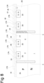
- Figure 6 illustrates a variant embodiment in which the circuit 12 comprises further first and second diodes 13A* 13B* in the chain.
- First diodes 13A, 13A* are arranged in series between the high voltage region HV and the node 14, and second diodes 13B 13B* are arranged in series between the node 14 and the low voltage region LV.
- the voltage drop across each diode 13 is smaller. This allows for voltage drops across each of the trenches 4,5 to be greater than the breakdown voltage of a single diode 13. It will be appreciated that this concept can be extended to include any number of additional diodes 13 into the chain.
- FIG. 5-7 illustrates embodiments with the same number of diodes arranged across each trench. Although this is the preferred method of implementation it is not essential.
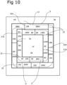
- circuit 12 (which is illustrated in Fig 10 highly schematically as a dashed line) connects between the high voltage region HV and the low voltage region LV.
- the circuit 12 comprises multiple diodes 13 connected in series with at least one diode formed in each division 6A-6H, 10A-10G of each sub-region 6,10, and a separate node connected to each division 6A-6H, 10A-10G of each sub-region 6,10 so that a different intermediate voltage is applied to each division 6A-6H, 10A-10G.
Landscapes
- Semiconductor Integrated Circuits (AREA)
- Element Separation (AREA)
- Metal-Oxide And Bipolar Metal-Oxide Semiconductor Integrated Circuits (AREA)
- Bipolar Transistors (AREA)
- Electrodes Of Semiconductors (AREA)
Claims (15)
- Un dispositif semi-conducteur comprenant une structure isolante visant à isoler une zone haute tension sur une surface semi-conductrice d'une zone basse tension sur la surface semi-conductrice ;la structure isolante comprenant :une première couche d'un premier type de semi-conducteur en contact avec une deuxième couche d'un second type de semi-conducteur ; la deuxième couche constituant la surface semi-conductrice ;un premier sillon et un second sillon situés entre les zones haute et basse tension pour isoler la zone haute tension de la zone basse tension ; chaque sillon, le premier et le second, s'étendant sur la surface semi-conductrice et traversant entièrement la seconde couche pour définir à cet endroit une sous-zone de la seconde couche entre les zones haute et basse tension, qui est isolée des zones haute et basse tension ; etle dispositif semi-conducteur comprenant un circuit qui établit une connexion entre la zone haute tension et la zone basse tension ; le circuit est agencé pour générer une tension intermédiaire ; le circuit comprenant une sortie connectée à la sous-zone pour appliquer la tension intermédiaire à la sous-zone ; la tension intermédiaire ayant une valeur comprise entre les valeurs des zones haute et basse tension respectives ;caractérisé par le fait que la structure isolante comprend un premier ensemble de sillons latéraux qui s'étendent dans la sous-zone, entre le premier et le second sillons, pour diviser la sous-zone en subdivisions et dans laquelle le circuit comprend une sortie séparée connectée à chaque subdivision pour appliquer une tension intermédiaire différente à chaque subdivision.
- Un dispositif semi-conducteur selon la revendication 1, dans lequel le circuit est un circuit intégré.
- Un dispositif semi-conducteur selon la revendication 1 ou 2, dans lequel le circuit comprend un composant électrique situé dans la sous-zone.
- Un dispositif semi-conducteur selon les revendications 1 à 3, dans lequel le circuit comprend une chaîne de composants électriques en série qui permet une série de chutes de tension, et la sortie est connectée électriquement à plusieurs composants électriques de la chaîne.
- Un dispositif semi-conducteur selon la revendication 4, dans lequel la chaîne de composants électriques à l'intérieur du système est orientée pour s'étendre le long de l'un ou des deux sillons, le premier et second.
- Un dispositif semi-conducteur selon la revendication 3, 4 ou 5, dans lequel le composant électrique comprend une diode.
- Un dispositif semi-conducteur selon la revendication 6, dans lequel la ou les diodes fonctionnent dans un état de polarisation inverse.
- Un dispositif semi-conducteur selon la revendication 7, dans lequel la ou les diodes sont des diodes Zener.
- Un dispositif semi-conducteur selon l'une des revendications 6, 7 ou 8, comprenant : une zone du premier type de semi-conducteur à l'intérieur de la couche du second type ; et une troisième couche se trouvant sur la surface semi-conductrice ; la structure est agencée de telle sorte qu'une partie de la troisième couche est en contact avec la zone du premier type de semi-conducteur pour former une j onction de diode et constituer une première diode, et la partie de la troisième couche s'étend sur le premier sillon pour établir une connexion électrique entre la diode et la sous-zone.
- Un dispositif semi-conducteur selon la revendication 9 dans lequel la structure comprend une autre zone du premier type de semi-conducteur à l'intérieur de la sous-zone de la deuxième couche ; et la partie de la troisième couche est également en contact avec l'autre zone du premier type de semi-conducteur pour former une seconde diode dans la sous-zone et pour assurer une connexion électrique entre la première diode et la deuxième diode.
- Un dispositif semi-conducteur selon l'une des revendications précédentes, dans lequel le premier et le second sillons sont disposés selon une formation imbriquée autour de la zone basse tension ou de la zone haute tension.
- Un dispositif semi-conducteur selon l'une des revendications précédentes, comprenant un troisième sillon se trouvant entre les zones haute et basse tension pour isoler la zone haute tension de la zone basse tension ; le troisième sillon s'étendant depuis la surface semi-conductrice à travers la deuxième couche et dans la première couche pour définir entre celle-ci et le premier sillon, une deuxième sous-zone de la deuxième couche entre les zones haute et basse tension qui est isolée des zones haute et basse tension ; et un dispositif pour appliquer une seconde tension intermédiaire à la sous-zone de la seconde couche ; la seconde tension intermédiaire ayant une valeur comprise entre la tension intermédiaire et celle de la zone haute tension.
- Un dispositif semi-conducteur selon les revendications 1 à 12 dans lequel le circuit génère la deuxième tension intermédiaire ; le circuit semi-conducteur comprend une seconde sortie connectée à la seconde sous-zone pour appliquer la seconde tension intermédiaire à la seconde sous-zone.
- Un dispositif semi-conducteur selon la revendication 1 dans lequel la structure isolante comprend un second ensemble de sillons latéraux qui s'étendent dans la deuxième sous-zone, entre le premier et le troisième sillons, pour diviser la deuxième sous-zone en subdivisions ; et dans lequel le circuit comprend également une sortie séparée connectée à chaque subdivision de la deuxième sous-zone pour appliquer une tension intermédiaire différente à chaque subdivision de la deuxième sous-zone.
- Un dispositif semi-conducteur selon la revendication 14 dans lequel le premier ensemble de sillons latéraux est décalé par rapport au deuxième ensemble de sillons latéraux autour du premier sillon.
Applications Claiming Priority (2)
| Application Number | Priority Date | Filing Date | Title |
|---|---|---|---|
| GBGB2001477.5A GB202001477D0 (en) | 2020-02-04 | 2020-02-04 | A structure and method for guarding a low voltage region of a semiconductor device from a high voltage region of the semiconductor device |
| PCT/GB2021/050250 WO2021156620A1 (fr) | 2020-02-04 | 2021-02-04 | Structure de semi-conducteur et procédé de protection d'une région de surface à basse tension d'une région de surface à haute tension |
Publications (3)
| Publication Number | Publication Date |
|---|---|
| EP4100996A1 EP4100996A1 (fr) | 2022-12-14 |
| EP4100996C0 EP4100996C0 (fr) | 2024-07-03 |
| EP4100996B1 true EP4100996B1 (fr) | 2024-07-03 |
Family
ID=69800043
Family Applications (1)
| Application Number | Title | Priority Date | Filing Date |
|---|---|---|---|
| EP21704914.7A Active EP4100996B1 (fr) | 2020-02-04 | 2021-02-04 | Structure de semi-conducteur et procédé de protection d'une région de surface à basse tension d'une région de surface à haute tension |
Country Status (6)
| Country | Link |
|---|---|
| US (1) | US12278264B2 (fr) |
| EP (1) | EP4100996B1 (fr) |
| CN (1) | CN115298811A (fr) |
| AU (1) | AU2021217205A1 (fr) |
| GB (1) | GB202001477D0 (fr) |
| WO (1) | WO2021156620A1 (fr) |
Families Citing this family (1)
| Publication number | Priority date | Publication date | Assignee | Title |
|---|---|---|---|---|
| EP4174922A1 (fr) * | 2021-10-29 | 2023-05-03 | Infineon Technologies Austria AG | Dispositif semi-conducteur haute tension |
Family Cites Families (8)
| Publication number | Priority date | Publication date | Assignee | Title |
|---|---|---|---|---|
| JP5729745B2 (ja) | 2009-09-15 | 2015-06-03 | ルネサスエレクトロニクス株式会社 | 半導体装置およびその製造方法 |
| US9224703B2 (en) * | 2013-09-24 | 2015-12-29 | Semiconductor Components Industries, Llc | Electronic device including a diode and a process of forming the same |
| US20150123240A1 (en) * | 2013-11-07 | 2015-05-07 | Addison R. Crockett | Semiconductor Device and Method of Forming Shallow P-N Junction with Sealed Trench Termination |
| EP2930743B1 (fr) * | 2014-04-11 | 2016-09-21 | Nxp B.V. | Structure d'isolation de semi-conducteur |
| TWI546970B (zh) * | 2014-05-13 | 2016-08-21 | 帥群微電子股份有限公司 | 半導體元件的終端結構及其製造方法 |
| JP6238234B2 (ja) | 2014-06-03 | 2017-11-29 | ルネサスエレクトロニクス株式会社 | 半導体装置 |
| CN109065539B (zh) | 2018-08-22 | 2020-10-27 | 电子科技大学 | 一种bcd半导体器件及其制造方法 |
| FR3101480B1 (fr) * | 2019-09-30 | 2021-10-29 | St Microelectronics Tours Sas | Tranchées isolantes pour les circuits ESD |
-
2020
- 2020-02-04 GB GBGB2001477.5A patent/GB202001477D0/en not_active Ceased
-
2021
- 2021-02-04 US US17/760,048 patent/US12278264B2/en active Active
- 2021-02-04 AU AU2021217205A patent/AU2021217205A1/en active Pending
- 2021-02-04 WO PCT/GB2021/050250 patent/WO2021156620A1/fr not_active Ceased
- 2021-02-04 CN CN202180021867.3A patent/CN115298811A/zh active Pending
- 2021-02-04 EP EP21704914.7A patent/EP4100996B1/fr active Active
Also Published As
| Publication number | Publication date |
|---|---|
| EP4100996A1 (fr) | 2022-12-14 |
| US20230062444A1 (en) | 2023-03-02 |
| WO2021156620A1 (fr) | 2021-08-12 |
| EP4100996C0 (fr) | 2024-07-03 |
| AU2021217205A1 (en) | 2022-09-01 |
| GB202001477D0 (en) | 2020-03-18 |
| CN115298811A (zh) | 2022-11-04 |
| US12278264B2 (en) | 2025-04-15 |
Similar Documents
| Publication | Publication Date | Title |
|---|---|---|
| US7842969B2 (en) | Low clamp voltage ESD device and method therefor | |
| CN116207095B (zh) | 瞬态电压抑制装置 | |
| US20140167101A1 (en) | Tvs with low capacitance & forward voltage drop with depleted scr as steering diode | |
| US20080299751A1 (en) | Schottky diode and method therefor | |
| EP0583037B1 (fr) | Composant de protection à semiconducteur | |
| US12040389B2 (en) | Tiled lateral thyristor | |
| US20160099306A1 (en) | Monolithic merged pin schottky diode structure | |
| US20160300828A1 (en) | Esd protection device | |
| CN110034115A (zh) | 晶体管布置及其生产方法 | |
| US5434445A (en) | Junction-isolated high-voltage MOS integrated device | |
| EP4100996B1 (fr) | Structure de semi-conducteur et procédé de protection d'une région de surface à basse tension d'une région de surface à haute tension | |
| US6891204B2 (en) | Semiconductor component having field-shaping regions | |
| US20040046225A1 (en) | Semiconductor power component | |
| US20230060885A1 (en) | Semiconductor device | |
| US4260910A (en) | Integrated circuits with built-in power supply protection | |
| RU2832996C1 (ru) | Полупроводниковая структура и способ защиты области низкого напряжения поверхности от области высокого напряжения поверхности | |
| US20020003236A1 (en) | Electrostatic discharge protective structure | |
| US5293063A (en) | Monolithic structure comprising two sets of bidirectional protection diodes | |
| EP4187601A1 (fr) | Dispositif semiconducteur et procédé de fabrication | |
| US8384126B2 (en) | Low voltage PNPN protection device | |
| EP0780900B1 (fr) | Dispositif semi-conducteur monolithique avec structure de bord et méthode de fabrication | |
| US9129809B2 (en) | Silicon controlled rectifier for high voltage applications | |
| KR830000497B1 (ko) | 고전압 접합 솔리드 스테이트 스위치 | |
| JP2858445B2 (ja) | 自己消弧型逆導通サイリスタ | |
| US20040178506A1 (en) | Integrated circuit |
Legal Events
| Date | Code | Title | Description |
|---|---|---|---|
| STAA | Information on the status of an ep patent application or granted ep patent |
Free format text: STATUS: UNKNOWN |
|
| STAA | Information on the status of an ep patent application or granted ep patent |
Free format text: STATUS: THE INTERNATIONAL PUBLICATION HAS BEEN MADE |
|
| PUAI | Public reference made under article 153(3) epc to a published international application that has entered the european phase |
Free format text: ORIGINAL CODE: 0009012 |
|
| STAA | Information on the status of an ep patent application or granted ep patent |
Free format text: STATUS: REQUEST FOR EXAMINATION WAS MADE |
|
| 17P | Request for examination filed |
Effective date: 20220905 |
|
| AK | Designated contracting states |
Kind code of ref document: A1 Designated state(s): AL AT BE BG CH CY CZ DE DK EE ES FI FR GB GR HR HU IE IS IT LI LT LU LV MC MK MT NL NO PL PT RO RS SE SI SK SM TR |
|
| DAV | Request for validation of the european patent (deleted) | ||
| DAX | Request for extension of the european patent (deleted) | ||
| STAA | Information on the status of an ep patent application or granted ep patent |
Free format text: STATUS: EXAMINATION IS IN PROGRESS |
|
| 17Q | First examination report despatched |
Effective date: 20231013 |
|
| GRAP | Despatch of communication of intention to grant a patent |
Free format text: ORIGINAL CODE: EPIDOSNIGR1 |
|
| STAA | Information on the status of an ep patent application or granted ep patent |
Free format text: STATUS: GRANT OF PATENT IS INTENDED |
|
| INTG | Intention to grant announced |
Effective date: 20240207 |
|
| RIN1 | Information on inventor provided before grant (corrected) |
Inventor name: KNIGHT, LUKE Inventor name: LIGHT, ROGER Inventor name: SUMMERLAND, DAVID |
|
| GRAS | Grant fee paid |
Free format text: ORIGINAL CODE: EPIDOSNIGR3 |
|
| GRAA | (expected) grant |
Free format text: ORIGINAL CODE: 0009210 |
|
| STAA | Information on the status of an ep patent application or granted ep patent |
Free format text: STATUS: THE PATENT HAS BEEN GRANTED |
|
| AK | Designated contracting states |
Kind code of ref document: B1 Designated state(s): AL AT BE BG CH CY CZ DE DK EE ES FI FR GB GR HR HU IE IS IT LI LT LU LV MC MK MT NL NO PL PT RO RS SE SI SK SM TR |
|
| REG | Reference to a national code |
Ref country code: CH Ref legal event code: EP |
|
| REG | Reference to a national code |
Ref country code: DE Ref legal event code: R096 Ref document number: 602021015133 Country of ref document: DE |
|
| U01 | Request for unitary effect filed |
Effective date: 20240703 |
|
| U07 | Unitary effect registered |
Designated state(s): AT BE BG DE DK EE FI FR IT LT LU LV MT NL PT SE SI Effective date: 20240712 |
|
| PG25 | Lapsed in a contracting state [announced via postgrant information from national office to epo] |
Ref country code: NO Free format text: LAPSE BECAUSE OF FAILURE TO SUBMIT A TRANSLATION OF THE DESCRIPTION OR TO PAY THE FEE WITHIN THE PRESCRIBED TIME-LIMIT Effective date: 20241003 |
|
| PG25 | Lapsed in a contracting state [announced via postgrant information from national office to epo] |
Ref country code: GR Free format text: LAPSE BECAUSE OF FAILURE TO SUBMIT A TRANSLATION OF THE DESCRIPTION OR TO PAY THE FEE WITHIN THE PRESCRIBED TIME-LIMIT Effective date: 20241004 Ref country code: PL Free format text: LAPSE BECAUSE OF FAILURE TO SUBMIT A TRANSLATION OF THE DESCRIPTION OR TO PAY THE FEE WITHIN THE PRESCRIBED TIME-LIMIT Effective date: 20240703 |
|
| PG25 | Lapsed in a contracting state [announced via postgrant information from national office to epo] |
Ref country code: IS Free format text: LAPSE BECAUSE OF FAILURE TO SUBMIT A TRANSLATION OF THE DESCRIPTION OR TO PAY THE FEE WITHIN THE PRESCRIBED TIME-LIMIT Effective date: 20241103 |
|
| PG25 | Lapsed in a contracting state [announced via postgrant information from national office to epo] |
Ref country code: CZ Free format text: LAPSE BECAUSE OF FAILURE TO SUBMIT A TRANSLATION OF THE DESCRIPTION OR TO PAY THE FEE WITHIN THE PRESCRIBED TIME-LIMIT Effective date: 20240703 Ref country code: HR Free format text: LAPSE BECAUSE OF FAILURE TO SUBMIT A TRANSLATION OF THE DESCRIPTION OR TO PAY THE FEE WITHIN THE PRESCRIBED TIME-LIMIT Effective date: 20240703 |
|
| PG25 | Lapsed in a contracting state [announced via postgrant information from national office to epo] |
Ref country code: ES Free format text: LAPSE BECAUSE OF FAILURE TO SUBMIT A TRANSLATION OF THE DESCRIPTION OR TO PAY THE FEE WITHIN THE PRESCRIBED TIME-LIMIT Effective date: 20240703 Ref country code: RS Free format text: LAPSE BECAUSE OF FAILURE TO SUBMIT A TRANSLATION OF THE DESCRIPTION OR TO PAY THE FEE WITHIN THE PRESCRIBED TIME-LIMIT Effective date: 20241003 |
|
| PG25 | Lapsed in a contracting state [announced via postgrant information from national office to epo] |
Ref country code: RS Free format text: LAPSE BECAUSE OF FAILURE TO SUBMIT A TRANSLATION OF THE DESCRIPTION OR TO PAY THE FEE WITHIN THE PRESCRIBED TIME-LIMIT Effective date: 20241003 Ref country code: PL Free format text: LAPSE BECAUSE OF FAILURE TO SUBMIT A TRANSLATION OF THE DESCRIPTION OR TO PAY THE FEE WITHIN THE PRESCRIBED TIME-LIMIT Effective date: 20240703 Ref country code: NO Free format text: LAPSE BECAUSE OF FAILURE TO SUBMIT A TRANSLATION OF THE DESCRIPTION OR TO PAY THE FEE WITHIN THE PRESCRIBED TIME-LIMIT Effective date: 20241003 Ref country code: IS Free format text: LAPSE BECAUSE OF FAILURE TO SUBMIT A TRANSLATION OF THE DESCRIPTION OR TO PAY THE FEE WITHIN THE PRESCRIBED TIME-LIMIT Effective date: 20241103 Ref country code: HR Free format text: LAPSE BECAUSE OF FAILURE TO SUBMIT A TRANSLATION OF THE DESCRIPTION OR TO PAY THE FEE WITHIN THE PRESCRIBED TIME-LIMIT Effective date: 20240703 Ref country code: GR Free format text: LAPSE BECAUSE OF FAILURE TO SUBMIT A TRANSLATION OF THE DESCRIPTION OR TO PAY THE FEE WITHIN THE PRESCRIBED TIME-LIMIT Effective date: 20241004 Ref country code: ES Free format text: LAPSE BECAUSE OF FAILURE TO SUBMIT A TRANSLATION OF THE DESCRIPTION OR TO PAY THE FEE WITHIN THE PRESCRIBED TIME-LIMIT Effective date: 20240703 Ref country code: CZ Free format text: LAPSE BECAUSE OF FAILURE TO SUBMIT A TRANSLATION OF THE DESCRIPTION OR TO PAY THE FEE WITHIN THE PRESCRIBED TIME-LIMIT Effective date: 20240703 |
|
| U20 | Renewal fee for the european patent with unitary effect paid |
Year of fee payment: 5 Effective date: 20250228 |
|
| PG25 | Lapsed in a contracting state [announced via postgrant information from national office to epo] |
Ref country code: SM Free format text: LAPSE BECAUSE OF FAILURE TO SUBMIT A TRANSLATION OF THE DESCRIPTION OR TO PAY THE FEE WITHIN THE PRESCRIBED TIME-LIMIT Effective date: 20240703 |
|
| PG25 | Lapsed in a contracting state [announced via postgrant information from national office to epo] |
Ref country code: SK Free format text: LAPSE BECAUSE OF FAILURE TO SUBMIT A TRANSLATION OF THE DESCRIPTION OR TO PAY THE FEE WITHIN THE PRESCRIBED TIME-LIMIT Effective date: 20240703 |
|
| PLBE | No opposition filed within time limit |
Free format text: ORIGINAL CODE: 0009261 |
|
| STAA | Information on the status of an ep patent application or granted ep patent |
Free format text: STATUS: NO OPPOSITION FILED WITHIN TIME LIMIT |
|
| 26N | No opposition filed |
Effective date: 20250404 |
|
| PG25 | Lapsed in a contracting state [announced via postgrant information from national office to epo] |
Ref country code: MC Free format text: LAPSE BECAUSE OF FAILURE TO SUBMIT A TRANSLATION OF THE DESCRIPTION OR TO PAY THE FEE WITHIN THE PRESCRIBED TIME-LIMIT Effective date: 20240703 |
|
| REG | Reference to a national code |
Ref country code: CH Ref legal event code: PL |
|
| PG25 | Lapsed in a contracting state [announced via postgrant information from national office to epo] |
Ref country code: CH Free format text: LAPSE BECAUSE OF NON-PAYMENT OF DUE FEES Effective date: 20250228 |
|
| PGFP | Annual fee paid to national office [announced via postgrant information from national office to epo] |
Ref country code: GB Payment date: 20251205 Year of fee payment: 6 |
|
| PG25 | Lapsed in a contracting state [announced via postgrant information from national office to epo] |
Ref country code: IE Free format text: LAPSE BECAUSE OF NON-PAYMENT OF DUE FEES Effective date: 20250204 |