EP4100991B1 - Ein massenspektrometer zur ladungsdetektion und entsprechende methode - Google Patents
Ein massenspektrometer zur ladungsdetektion und entsprechende methode Download PDFInfo
- Publication number
- EP4100991B1 EP4100991B1 EP21750498.4A EP21750498A EP4100991B1 EP 4100991 B1 EP4100991 B1 EP 4100991B1 EP 21750498 A EP21750498 A EP 21750498A EP 4100991 B1 EP4100991 B1 EP 4100991B1
- Authority
- EP
- European Patent Office
- Prior art keywords
- ion
- charge
- signal
- measurement signal
- time window
- Prior art date
- Legal status (The legal status is an assumption and is not a legal conclusion. Google has not performed a legal analysis and makes no representation as to the accuracy of the status listed.)
- Active
Links
Images


Classifications
-
- H—ELECTRICITY
- H01—ELECTRIC ELEMENTS
- H01J—ELECTRIC DISCHARGE TUBES OR DISCHARGE LAMPS
- H01J49/00—Particle spectrometers or separator tubes
- H01J49/26—Mass spectrometers or separator tubes
- H01J49/34—Dynamic spectrometers
- H01J49/42—Stability-of-path spectrometers, e.g. monopole, quadrupole, multipole, farvitrons
- H01J49/4205—Device types
- H01J49/422—Two-dimensional RF ion traps
-
- H—ELECTRICITY
- H01—ELECTRIC ELEMENTS
- H01J—ELECTRIC DISCHARGE TUBES OR DISCHARGE LAMPS
- H01J49/00—Particle spectrometers or separator tubes
- H01J49/0027—Methods for using particle spectrometers
-
- H—ELECTRICITY
- H01—ELECTRIC ELEMENTS
- H01J—ELECTRIC DISCHARGE TUBES OR DISCHARGE LAMPS
- H01J49/00—Particle spectrometers or separator tubes
- H01J49/02—Details
- H01J49/025—Detectors specially adapted to particle spectrometers
-
- H—ELECTRICITY
- H01—ELECTRIC ELEMENTS
- H01J—ELECTRIC DISCHARGE TUBES OR DISCHARGE LAMPS
- H01J49/00—Particle spectrometers or separator tubes
- H01J49/02—Details
- H01J49/025—Detectors specially adapted to particle spectrometers
- H01J49/027—Detectors specially adapted to particle spectrometers detecting image current induced by the movement of charged particles
-
- H—ELECTRICITY
- H01—ELECTRIC ELEMENTS
- H01J—ELECTRIC DISCHARGE TUBES OR DISCHARGE LAMPS
- H01J49/00—Particle spectrometers or separator tubes
- H01J49/26—Mass spectrometers or separator tubes
- H01J49/34—Dynamic spectrometers
- H01J49/42—Stability-of-path spectrometers, e.g. monopole, quadrupole, multipole, farvitrons
- H01J49/4205—Device types
- H01J49/4245—Electrostatic ion traps
Definitions
- the present disclosure relates generally to charge detection mass spectrometry instruments, and more specifically to performing mass and charge measurements with such instruments.
- Charge detection mass spectrometry is a particle analysis technique in which the mass of an ion is determined by simultaneously measuring its mass-to-charge ratio, typically referred to as "m/z," and charge.
- m/z mass-to-charge ratio
- ELIT electrostatic linear ion trap
- Examples of known mass spectrometers are disclosed in WO 2019/140233A1 , WO 2019/236142A1 and WO 2019/231854A1 each disclosing CDMS in an ELIT.
- the present invention provides a method for measuring the charge of an ion in an electrostatic linear ion trap according to claim 1.
- the present invention provides a charge detection mass spectrometer according to claim 10.
- This disclosure relates to apparatuses and techniques for processing time-domain ion measurement signals, produced by an electrostatic linear ion trap (ELIT) of a charge detection mass spectrometer (CDMS), to simultaneously determine ion mass-to-charge ratio and ion charge from which ion mass can then be determined.
- ELIT electrostatic linear ion trap
- CDMS charge detection mass spectrometer
- charge detection event is defined as detection of a charge induced on a charge detector of the ELIT by an ion passing a single time through the charge detector
- ion measurement event is defined as a collection of charge detection events resulting from oscillation of an ion back and forth through the charge detector a selected number of times or for a selected time period.
- the phrase “ion measurement event” may alternatively be referred to herein as an “ion trapping event” or simply as a “trapping event,” and the phrases “ion measurement event,” “ion trapping event”, “trapping event” and variants thereof shall be understood to be synonymous with one another.
- a CDMS system 10 including an embodiment of an electrostatic linear ion trap (ELIT) 14 with control and measurement components coupled thereto.
- the CDMS system 10 includes an ion source 12 operatively coupled to an inlet of the ELIT 14.
- the ion source 12 illustratively includes any conventional device or apparatus for generating ions from a sample and may further include one or more devices and/or instruments for separating, collecting, filtering, fragmenting and/or normalizing or shifting charge states of ions according to one or more molecular characteristics.
- the ion source 12 may include a conventional electrospray ionization source, a matrix-assisted laser desorption ionization (MALDI) source or the like, coupled to an inlet of a conventional mass spectrometer.
- a conventional electrospray ionization source e.g., a plasma source or the like
- MALDI matrix-assisted laser desorption ionization
- the mass spectrometer may be of any conventional design including, for example, but not limited to a time-of-flight (TOF) mass spectrometer, a reflectron mass spectrometer, a Fourier transform ion cyclotron resonance (FTICR) mass spectrometer, a quadrupole mass spectrometer, a triple quadrupole mass spectrometer, a magnetic sector mass spectrometer, or the like.
- TOF time-of-flight
- FTICR Fourier transform ion cyclotron resonance
- the ion outlet of the mass spectrometer is operatively coupled to an ion inlet of the ELIT 14.
- the sample from which the ions are generated may be any biological or other material.
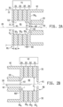
- the ELIT 14 includes a charge detector CD surrounded by a ground chamber or cylinder GC and operatively coupled to opposing ion mirrors M1, M2 respectively positioned at opposite ends thereof.
- the ion mirror M1 is operatively positioned between the ion source 12 and one end of the charge detector CD, and ion mirror M2 is operatively positioned at the opposite end of the charge detector CD.
- Each ion mirror M1, M2 defines a respective ion mirror region R1, R2 therein.
- the regions R1, R2 of the ion mirrors M1, M2, the charge detector CD, and the spaces between the charge detector CD and the ion mirrors M1, M2 together define a longitudinal axis 20 centrally therethrough which illustratively represents an ideal ion travel path through the ELIT 14 and between the ion mirrors M1, M2 as will be described in greater detail below.
- voltage sources V1, V2 are electrically connected to the ion mirrors M1, M2 respectively.
- Each voltage source V1, V2 illustratively includes one or more switchable DC voltage sources which may be controlled or programmed to selectively produce a number, N, programmable or controllable voltages, wherein N may be any positive integer. Illustrative examples of such voltages will be described below with respect to FIGS. 2A and 2B to establish one of two different operating modes of each of the ion mirrors M1, M2 as will be described in detail below.
- ions move within the ELIT 14 close to the longitudinal axis 20 extending centrally through the charge detector CD and the ion mirrors M1, M2 under the influence of electric fields selectively established by the voltage sources V1, V2.
- the voltage sources V1, V2 are illustratively shown electrically connected by a number, P, of signal paths to a conventional processor 16 including a memory 18 having instructions stored therein which, when executed by the processor 16, cause the processor 16 to control the voltage sources V1, V2 to produce desired DC output voltages for selectively establishing ion transmission and ion reflection electric fields, TEF, REF respectively, within the regions R1, R2 of the respective ion mirrors M1, M2.
- P may be any positive integer.
- either or both of the voltage sources V1, V2 may be programmable to selectively produce one or more constant output voltages.
- either or both of the voltage sources V1, V2 may be configured to produce one or more time-varying output voltages of any desired shape. It will be understood that more or fewer voltage sources may be electrically connected to the mirrors M1, M2 in alternate embodiments.
- the charge detector CD is illustratively provided in the form of an electrically conductive cylinder which is electrically connected to a signal input of a charge sensitive preamplifier CP, and the signal output of the charge-sensitive preamplifier CP is electrically connected to the processor 16.
- the voltage sources V1, V2 are illustratively controlled in a manner, as described in detail below, which selectively traps an ion entering the ELIT 14 and causes it to oscillate therein back and forth between the ion mirrors M1, M2 such that the trapped ion repeatedly passes through the charge detector CD.
- the charge sensitive preamplifier CP is illustratively operable in a conventional manner to detect charges (CH) induced on the charge detection cylinder CD as the ion passes through the charge detection cylinder CD between the ion mirrors M1, M2, to produce charge detection signals (CHD) corresponding thereto.
- the charge detection signals CHD are illustratively recorded in the form of oscillation period values and, in this regard, each oscillation period value represents ion measurement information for a single, respective charge detection event.
- a plurality of such oscillation period values are measured and recorded for the trapped ion during a respective ion measurement event (i.e., during an ion trapping event), and the resulting plurality of recorded oscillation period values i.e., the collection of recorded ion measurement information, for the ion measurement event, is processed to determine ion charge, mass-to-charge ratio and/or mass values as will be described below. Multiple ion measurement events can be processed in this manner, and a mass-to-charge ratio and/or mass spectrum of the sample may illustratively be constructed therefrom.
- ion mirrors M1, M2 are identical to one another in that each includes a cascaded arrangement of 4 spaced-apart, electrically conductive mirror electrodes.
- a first mirror electrode 30 1 has a thickness W1 and defines a passageway centrally therethrough of diameter P1.
- An endcap 32 is affixed or otherwise coupled to an outer surface of the first mirror electrode 30 1 and defines an aperture A1 centrally therethrough which serves as an ion entrance and/or exit to and/or from the corresponding ion mirror M1, M2 respectively.
- the endcap 32 is coupled to, or is part of, an ion exit of the ion source 12 illustrated in FIG. 1 .
- the aperture A1 for each endcap 32 illustratively has a diameter P2.
- a second mirror electrode 30 2 of each ion mirror M1, M2 is spaced apart from the first mirror electrode 30 1 by a space having width W2.
- the second mirror electrode 30 2 like the mirror electrode 30 1 , has thickness W1 and defines a passageway centrally therethrough of diameter P2.
- a third mirror electrode 30 3 of each ion mirror M1, M2 is likewise spaced apart from the second mirror electrode 30 2 by a space of width W2.
- the third mirror electrode 30 3 has thickness W1 and defines a passageway centrally therethrough of width P1.
- a fourth mirror electrode 30 4 is spaced apart from the third mirror electrode 30s by a space of width W2.
- the fourth mirror electrode 30 4 illustratively has a thickness of W1 and is formed by a respective end of the ground cylinder, GC disposed about the charge detector CD.
- the fourth mirror electrode 30 4 defines an aperture A2 centrally therethrough which is illustratively conical in shape and increases linearly between the internal and external faces of the ground cylinder GC from a diameter P3 defined at the internal face of the ground cylinder GC to the diameter P1 at the external face of the ground cylinder GC (which is also the internal face of the respective ion mirror M1, M2).
- the spaces defined between the mirror electrodes 30 1 - 30 4 may be voids in some embodiments, i.e., vacuum gaps, and in other embodiments such spaces may be filled with one or more electrically non-conductive, e.g., dielectric, materials.
- the mirror electrodes 30 1 - 30 4 and the endcaps 32 are axially aligned, i.e., collinear, such that a longitudinal axis 22 passes centrally through each aligned passageway and also centrally through the apertures A1, A2.
- the spaces between the mirror electrodes 30 1 - 30 4 include one or more electrically non-conductive materials
- such materials will likewise define respective passageways therethrough which are axially aligned, i.e., collinear, with the passageways defined through the mirror electrodes 30 1 - 30 4 and which illustratively have diameters of P2 or greater.
- P1 > P3 > P2 although in other embodiments other relative diameter arrangements are possible.
- a region R1 is defined between the apertures A1, A2 of the ion mirror M1, and another region R2 is likewise defined between the apertures A1, A2 of the ion mirror M2.
- the regions R1, R2 are illustratively identical to one another in shape and in volume.
- the charge detector CD is illustratively provided in the form of an elongated, electrically conductive cylinder positioned and spaced apart between corresponding ones of the ion mirrors M1, M2 by a space of width W3.
- P1 > P3 > P2 although in alternate embodiments other relative width arrangements are possible.
- the longitudinal axis 20 illustratively extends centrally through the passageway defined through the charge detection cylinder CD, such that the longitudinal axis 20 extends centrally through the combination of the ion mirrors M1, M2 and the charge detection cylinder CD.
- the ground cylinder GC is illustratively controlled to ground potential such that the fourth mirror electrode 30 4 of each ion mirror M1, M2 is at ground potential at all times.
- the fourth mirror electrode 30 4 of either or both of the ion mirrors M1, M2 may be set to any desired DC reference potential, or to a switchable DC or other time-varying voltage source.
- the voltage sources V1, V2 are each configured to each produce four DC voltages D1 - D4, and to supply the voltages D1 - D4 to a respective one of the mirror electrodes 30 1 - 30 4 of the respective ion mirror M1, M2.
- the one or more such mirror electrodes 30 1 - 30 4 may alternatively be electrically connected to the ground reference of the respective voltage supply V1, V2 and the corresponding one or more voltage outputs D1 - D4 may be omitted.
- any two or more of the mirror electrodes 30 1 - 30 4 may be electrically connected to a single one of the voltage outputs D1 - D4 and superfluous ones of the output voltages D1 - D4 may be omitted.
- Each ion mirror M1, M2 is illustratively controllable and switchable, by selective application of the voltages D1 - D4, between an ion transmission mode ( FIG. 2A ) in which the voltages D1 - D4 produced by the respective voltage source V1, V2 establishes an ion transmission electric field (TEF) in the respective region R1, R2 thereof, and an ion reflection mode ( FIG. 2B ) in which the voltages D1 - D4 produced by the respect voltage source V1, V2 establishes an ion reflection electric field (REF) in the respective region R1, R2 thereof.
- TEZ ion transmission electric field
- FIG. 2B ion reflection mode
- An identical ion transmission electric field TEF may be selectively established within the region R2 of the ion mirror M2 via like control of the voltages D1 - D4 of the voltage source V2.
- an ion entering the region R2 from the charge detection cylinder CD via the aperture A2 of M2 is focused toward the longitudinal axis 20 by the ion transmission electric field TEF within the region R2 so that the ion exits the aperture A1 of the ion mirror M2.
- an ion reflection electric field REF established in the region R2 of the ion mirror M2 via selective control of the voltages D1 - D4 of V2 acts to decelerate and stop an ion entering the ion region R2 from the charge detection cylinder CD via the ion inlet aperture A2 of M2, to accelerate the stopped ion in the opposite direction back through the aperture A2 of M2 and into the end of the charge detection cylinder CD adjacent to M2 as depicted by the ion trajectory 42, and to focus the ion toward the central, longitudinal axis 20 within the region R2 of the ion mirror M2 so as to maintain a narrow trajectory of the ion back through the charge detector CD toward the ion mirror M1.
- An identical ion reflection electric field REF may be selectively established within the region R1 of the ion mirror M1 via like control of the voltages D1 - D4 of the voltage source V1.
- an ion entering the region R1 from the charge detection cylinder CD via the aperture A2 of M1 is decelerated and stopped by the ion reflection electric field REF established within the region R1, then accelerated in the opposite direction back through the aperture A2 of M1 and into the end of the charge detection cylinder CD adjacent to M1, and focused toward the central, longitudinal axis 20 within the region R1 of the ion mirror M1 so as to maintain a narrow trajectory of the ion back through the charge detector CD toward the ion mirror M1.
- An ion that traverses the length of the ELIT 14 and is reflected by the ion reflection electric field REF in the ion regions R1, R2 in a manner that enables the ion to continue traveling back and forth through the charge detection cylinder CD between the ion mirrors M1, M2 as just described is considered to be trapped within the ELIT 14.
- Example sets of output voltages D1 - D4 produced by the voltage sources V1, V2 respectively to control a respective ion mirrors M1, M2 to the ion transmission and reflection modes described above are shown in TABLE I below. It will be understood that the following values of D1 - D4 are provided only by way of example, and that other values of one or more of D1 - D4 may alternatively be used.
- the ion mirrors M1, M2 and the charge detection cylinder CD are illustrated in FIGS. 1 - 2B as defining cylindrical passageways therethrough, it will be understood that in alternate embodiments either or both of the ion mirrors M1, M2 and/or the charge detection cylinder CD may define non-cylindrical passageways therethrough such that one or more of the passageway(s) through which the longitudinal axis 20 centrally passes represents a cross-sectional area and profile that is not circular. In still other embodiments, regardless of the shape of the cross-sectional profiles, the cross-sectional areas of the passageway defined through the ion mirror M1 may be different from the passageway defined through the ion mirror M2.
- the processor 16 includes a conventional amplifier circuit 40 having an input receiving the charge detection signal CHD produced by the charge sensitive preamplifier CP and an output electrically connected to an input of a conventional Analog-to-Digital (A/D) converter 42. An output of the A/D converter 42 is electrically connected to a processor 50 (P1).
- the amplifier 40 is operable in a conventional manner to amplify the charge detection signal CHD produced by the charge sensitive preamplifier CP, and the A/D converter is, in turn, operable in a conventional manner to convert the amplified charge detection signal to a digital charge detection signal CDS.
- the processor 16 illustrated in FIG. 3 further includes a conventional comparator 44 having a first input receiving the charge detection signal CHD produced by the charge sensitive preamplifier CP, a second input receiving a threshold voltage CTH produced by a threshold voltage generator (TG) 46 and an output electrically connected to the processor 50.
- the comparator 44 is operable in a conventional manner to produce a trigger signal TR at the output thereof which is dependent upon the magnitude of the charge detection signal CDH relative to the magnitude of the threshold voltage CTH.
- the comparator 44 is operable to produce an "inactive" trigger signal TR at or near a reference voltage, e.g., ground potential, as long as CHD is less than CTH, and is operable to produce an "active" TR signal at or near a supply voltage of the circuitry 40, 42, 44, 46, 50 or otherwise distinguishable from the inactive TR signal when CHD is at or exceeds CTH.
- the comparator 44 may be operable to produce an "inactive" trigger signal TR at or near the supply voltage as long as CHD is less than CTH, and is operable to produce an "active" trigger signal TR at or near the reference potential when CHD is at or exceeds CTH.
- the comparator 44 may additionally be designed in a conventional manner to include a desired amount of hysteresis to prevent rapid switching of the output between the reference and supply voltages.
- the processor 50 is illustratively operable to produce a threshold voltage control signal THC and to supply THC to the threshold generator 46 to control operation thereof.
- the processor 50 is programmed or programmable to control production of the threshold voltage control signal THC in a manner which controls the threshold voltage generator 46 to produce CTH with a desired magnitude and/or polarity.
- a user may provide the processor 50 with instructions in real time, e.g., through a downstream processor, e.g., via a virtual control and visualization unit, to control production of the threshold voltage control signal THC in a manner which controls the threshold voltage generator 46 to produce CTH with a desired magnitude and/or polarity.
- the threshold voltage generator 46 is illustratively implemented, in some embodiments, in the form of a conventional controllable DC voltage source configured to be responsive to a digital form of the threshold control signal THC, e.g., in the form of a single serial digital signal or multiple parallel digital signals, to produce an analog threshold voltage CTH having a polarity and a magnitude defined by the digital threshold control signal THC.
- the threshold voltage generator 46 may be provided in the form of a conventional digital-to-analog (D/A) converter responsive to a serial or parallel digital threshold voltage TCH to produce an analog threshold voltage CTH having a magnitude, and in some embodiments a polarity, defined by the digital threshold control signals THC.
- D/A digital-to-analog
- the D/A converter may form part of the processor 50.
- the D/A converter may form part of the processor 50.
- Those skilled in the art will recognize other conventional circuits and techniques for selectively producing the threshold voltage CTH of desired magnitude and/or polarity in response to one or more digital and/or analog forms of the control signal THC, and it will be understood that any such other conventional circuits and/or techniques are intended to fall within the scope of this disclosure.
- the processor 50 is further operable to control the voltage sources V1, V2 as described above with respect to FIGS. 2A, 2B to selectively establish ion transmission and reflection fields within the regions R1, R2 of the ion mirrors M1, M2 respectively.
- the processor 50 is programmed or programmable to control the voltage sources V1, V2.
- the voltage source(s) V1 and/or V2 may be programmed or otherwise controlled in real time by a user, e.g., through a downstream processor 52, e.g., via a virtual control and visualization unit.
- the processor 50 is, in one embodiment, illustratively provided in the form of a field programmable gate array (FPGA) programmed or otherwise instructed by a user to collect and store charge detection signals CDS for charge detection events and for ion measurement events, to produce the threshold control signal(s) TCH from which the magnitude and/or polarity of the threshold voltage CTH is determined or derived, and to control the voltage sources V1, V2.
- FPGA field programmable gate array
- the memory 18 described with respect to FIG. 1 is integrated into, and forms part of, the programming of the FPGA.
- the processor 50 may be provided in the form of one or more conventional microprocessors or controllers and one or more accompanying memory units having instructions stored therein which, when executed by the one or more microprocessors or controllers, cause the one or more microprocessors or controllers to operate as just described.
- the processing circuit 50 may be implemented purely in the form of one or more conventional hardware circuits designed to operate as described above, or as a combination of one or more such hardware circuits and at least one microprocessor or controller operable to execute instructions stored in memory to operate as described above.
- the embodiment of the processor 16 depicted in FIG. 3 further illustratively includes a second processor 52 coupled to the first processor 50 and also to at least one memory unit 54.
- the processor 52 may include one or more peripheral devices, such as a display monitor, one or more input and/or output devices or the like, although in other embodiments the processor 52 may not include any such peripheral devices.
- the processor 52 is illustratively configured, i.e., programmed, to execute at least one process for analyzing ion measurement events.
- Data in the form of charge magnitude and charge timing data (i.e., detection of the timing of charges induced by the ion on the charge detection cylinder relative to one another) received by the processor 50 via the charge detection signals CDS is illustratively transferred from the processor 50 directly to the processor 52 for processing and analysis upon completion of each ion measurement event.
- the processor 52 is illustratively provided in the form of a high-speed server operable to perform both collection/storage and analysis of such data.
- one or more high-speed memory units 54 are coupled to the processor 52, and is/are operable to store data received and analyzed by the processor 52.
- the one or more memory units 54 illustratively include at least one local memory unit for storing data being used or to be used by the processor 52, and at least one permanent storage memory unit for storing data long term.
- the processor 52 is illustratively provided in the form of a Linux ® server (e.g., OpenSuse Leap 42.1) with four Intel ® Xeon TM processors (e.g., E5-465L v2, 12 core, 2.4 GHz).
- a Linux ® server e.g., OpenSuse Leap 42.1
- Intel ® Xeon TM processors e.g., E5-465L v2, 12 core, 2.4 GHz.
- an improvement in the average analysis time of a single ion measurement event file of over 100x is realized as compared with a conventional Windows ® PC (e.g., i5-2500K, 4 cores, 3.3 GHz).
- the processor 52 of this embodiment together with high speed/high performance memory unit(s) 54 illustratively provide for an improvement of over 100x in data storage speed.
- the processor 52 may be provided in the form of one or more conventional microprocessors or controllers and one or more accompanying memory units having instructions stored therein which, when executed by the one or more microprocessors or controllers, cause the one or more microprocessors or controllers to operate as described herein.
- the memory unit 54 illustratively has instructions stored therein which are executable by the processor 52 to analyze ion measurement event data produced by the ELIT 14 to determine ion mass spectral information for a sample under analysis.
- the processor 52 is operable to receive ion measurement event data from the processor 50 in the form of charge magnitude and charge detection timing information measured during each of multiple "charge detection events" (as this term is defined above) making up the "ion measurement event" (as this term is defined above), and to process such charge detection events making up such an ion measurement event to determine ion charge and mass-to-charge data, and to then determine ion mass data therefrom. Multiple ion measurement events may be processed in like manner to create mass spectral information for the sample under analysis.
- the voltage sources V1, V2 are illustratively controlled by the processor 50, e.g., via the processor 52, in a manner which selectively establishes ion transmission and ion reflection electric fields in the region R1 of the ion mirror M1 and in the region R2 of the ion mirror M2 to guide ions introduced into the ELIT 14 from the ion source 12 through the ELIT 14, and to then cause a single ion to be selectively trapped and confined within the ELIT 14 such that the trapped ion repeatedly passes through the charge detector CD as it oscillates back and forth between M1 and M2.
- FIG. 1 simplified diagrams of the ELIT 14 of FIG. 1 are shown depicting an example of such sequential control and operation of the ion mirrors M1, M2 of the ELIT 14.
- the processor 52 will be described as controlling the operation of the voltage sources V1, V2 in accordance with its programming, although it will be understood that the operation of the voltage source V1 and/or the operation of the voltage source V2 may be virtually controlled, at least in part, by the processor 50.
- the ELIT control sequence begins with the processor 52 controlling the voltage source V1 to control the ion mirror M1 to the ion transmission mode of operation (T) by establishing an ion transmission field within the region R1 of the ion mirror M1, and also controlling the voltage source V2 to control the ion mirror M2 to the ion transmission mode of operation (T) by likewise establishing an ion transmission field within the region R2 of the ion mirror M2.
- ions generated by the ion source 12 pass into the ion mirror M1 and are focused by the ion transmission field established in the region R1 toward the longitudinal axis 20 as they pass into the charge detection cylinder CD.
- the ions then pass through the charge detection cylinder CD and into the ion mirror M2 where the ion transmission field established within the region R2 of M2 focusses the ions toward the longitudinal axis 20 such that the ions pass through the exit aperture A1 of M2 as illustrated by the ion trajectory 60 depicted in FIG. 4A .
- the processor 52 is illustratively operable to control the voltage source V2 to control the ion mirror M2 to the ion reflection mode (R) of operation by establishing an ion reflection field within the region R2 of the ion mirror M2, while maintaining the ion mirror M1 in the ion transmission mode (T) of operation as shown.
- At least one ion generated by the ion source 12 enters into the ion mirror M1 and is focused by the ion transmission field established in the region R1 toward the longitudinal axis 20 such that the at least one ion passes through the ion mirror M1 and into the charge detection cylinder CD as just described with respect to FIG. 4A .
- the ion(s) then pass(es) through the charge detection cylinder CD and into the ion mirror M2 where the ion reflection field established within the region R2 of M2 reflects the ion(s) to cause it/them to travel in the opposite direction and back into the charge detection cylinder CD, as illustrated by the ion trajectory 62 in FIG. 4B .
- the processor 52 is operable to control the voltage source V1 to control the ion mirror M1 to the ion reflection mode (R) of operation by establishing an ion reflection field within the region R1 of the ion mirror M1, while maintaining the ion mirror M2 in the ion reflection mode (R) of operation in order to trap the ion(s) within the ELIT 14.
- the processor 52 is illustratively operable, i.e., programmed, to control the ELIT 14 in a "random trapping mode" or “continuous trapping mode” in which the processor 52 is operable to control the ion mirror M1 to the reflection mode (R) of operation after the ELIT 14 has been operating in the state illustrated in FIG. 4B , i.e., with M1 in ion transmission mode and M2 in ion reflection mode, for a selected time period. Until the selected time period has elapsed, the ELIT 14 is controlled to operate in the state illustrated in FIG. 4B .
- the processor 52 is operable, i.e., programmed, to control the ELIT 14 in a "trigger trapping mode" which illustratively carries a substantially greater probability of trapping a single ion therein as compared to the random trapping mode.
- the processor 52 is operable to control the ion mirror M1 to the reflection mode (R) of operation after an ion has been detected as passing through the charge detection cylinder CD.
- the processor 50 is operable to maintain the operating state illustrated in FIG. 4C until the ion passes through the charge detection cylinder CD a selected number of times. In an alternate embodiment, the processor 50 is operable to maintain the operating state illustrated in FIG.
- the number of cycles or time spent in the state illustrated in FIG. 4C may illustratively be programmed, e.g., via instructions stored in the memory 54, or controlled via a user interface, and in any case the ion detection event information resulting from each pass by the ion through the charge detection cylinder CD is temporarily stored in the processor 50, e.g., in the form of an ion measurement file which may illustratively have a predefined data or sample length.
- the total number of charge detection events stored in the processor 50 defines an ion measurement event and, upon completion of the ion measurement event, the stored ion detection events defining the ion measurement event, e.g., the ion measurement event file, is passed to, or retrieved by, the processor 52.
- the sequence illustrated in FIGS. 4A - 4C then returns to that illustrated in FIG.
- ion measurement event files were analyzed in the frequency domain using a Fast Fourier Transform (FFT) algorithm.
- FFT Fast Fourier Transform
- the mass-to-charge ratio (m/z) of the ion was calculated from the fundamental oscillation frequency (f0) of the signal using a calibration constant (C) (Equation 1), and the charge of the ion was determined by the magnitude of the fundamental frequency peak in the FFT.
- m z C f 0 2
- the signal can be thought of as being expressed as only a single sine wave.
- a significant amount of information about the signal is unused by the FFT because higher order harmonics are disregarded. This means the signal must be measured for longer to obtain charge-state resolution. Expressing the waveform more completely would decrease the amplitude uncertainty, therefore improving the charge precision and reducing the trapping time that is necessary to reach charge-state resolution.
- the peak magnitude in FFT analysis depends on factors like the signal duty cycle, the time domain signal amplitude is constant for a given charge and the amplitude measurement in the time domain is independent of the duty cycle.
- time domain analysis advantageous for applications with time-variant signal transients such as those found in CDMS where the ion oscillation frequency and the signal duty cycle change as the ion loses energy by collisions with the background gas and electrostatic interactions with the detection cylinder.
- the ELIT is designed such that the time-domain charge detection signals CHD stored in the ion measurement event files are squarewave signals (i.e., with 50% duty cycle), although it will be understood that in alternate implementations the ELIT may be designed such that the duty cycle of the time-domain charge detection signals CHD is greater or less than 50%.
- the following algorithm improves the charge magnitude determination precision by 15% to 20% compared to the FFT, reaching the statistical lower limit for amplitude uncertainty for a square wave corrupted with Gaussian noise.
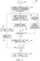
- FIG. 5 a simplified flow diagram is shown of an embodiment of a process 100 for analyzing the signal measurements contained in an ion measurement event file in the time domain to determine the frequency and the charge magnitude (z) of the ion oscillating back and forth through the charge detection cylinder of the ELIT during an ion trapping event. From this frequency determination, the mass-to-charge ratio (m/z) of the ion is determined from equation 1, and the mass of the ion is determined as a product of m/z and z.
- the process 100 is stored in the memory of the processor 16 in the form of instructions executable by the processor 16 to carry out the functionality of the process 100.
- the process 100 begins at step 102 where a time window counter, N, is initialized to 1 (or some other constant value).
- the process 100 is illustratively designed to analyze the signal measurements contained in an ion measurement event file by analyzing signal measurements in each of a plurality of sequential time windows of the measurement event file.
- This file windowing approach advantageously reduces the effect of a time-varying frequency and duty cycle on the measured amplitudes as long as the frequency and duty cycle of the signal measurements do not substantially change in each time window, thereby allowing for an approximation of these parameters to be constant for the duration of each window.
- the time windows are illustratively selected to each be 10 ms in length with each of the 10 time windows contain 100 cycles of signal measurements.
- step 104 the processor 16 is operable to perform an FFT analysis of the 1 st time window of the signal measurements contained in an ion measurement event file (hereinafter ion measurement signal IMS), and to determine the fundamental oscillation frequency (F FFT ) and the charge magnitude (CH FFT ) of the 1 st time window of the IMS signal in a conventional manner as described above.
- F FFT fundamental oscillation frequency
- CH FFT charge magnitude
- CH FFT is multiplied by 2.955 ADC bits/e to obtain the time domain signal amplitude in ADC bits for later use in the process 100.
- step 106 the processor 16 is operable to generate a simulated ion signal (SIS) for the Nth time window using input parameters F, CH, PH and DC, where F is frequency, CH is charge magnitude, PH is phase and DC is duty cycle.
- SIS simulated ion signal
- SIS was generated by simulating in the ELIT a trajectory of one 130 eV/z ion with an m/z of 25,600 TH using a Beeman algorithm (a modified Velocity Verlet algorithm) in Fortran at 10.02306 kHz using electric fields calculated by SIMION 8.1.
- the signal for that ion was generated by superimposing the ion trajectory over a potential array where the charge detection cylinder has +1 and all other electrodes are held at ground. This generates a signal 160 that is normalized to +1 in accordance with Green's Reciprocity Theorem as depicted by example in FIG. 6 .
- the signal 160 is broken up into two sections; 1 negative-going transition 160A and a positive-going transition 160B.
- One period of the signal was fit using two bi-dose sigmoidal curves in OriginPro 2018.
- f scaling is the desired frequency divided by the nominal frequency used in initially creating an analytical function for this waveform (e.g., 10.02306 kHz).
- An example such analytical function is illustrated in FIG. 8 in which the signal 160 is variable between a lower frequency 180A, e.g., 10 kHz, and a higher frequency 180B, e.g., 15 kHz.
- T is the wave period duration
- the time that has elapsed since the last wave period has begun is t-t 0
- A is the amplitude.
- Phase is adjusted by adding a phase time to t 0 which shifts the waveform by a specified time.
- the variables h 1 and h 2 describe the rate at which a wave transitions between LO to HI or HI to LO states.
- the variable h scaling multiplicatively adjusts h to adjust the transition slope.
- the minima and maxima for these curves were constrained to 0 and +1, respectively so they could be concatenated end-to-end to generate a periodic waveform.
- the SIS waveform was then scaled to an amplitude of 1500 ADC bits and centered around zero.
- a decay constant multiplied by the symmetric numerical derivative of the waveform generated the RC-decayed point i of the SIS waveform function in accordance with the following equation.
- SIS i ⁇ ⁇ ⁇ ⁇ t SIS i + 1 ⁇ SIS i ⁇ 1 2
- the ⁇ constant was determined by applying a square wave produced by a function generator to an antenna in proximity to the charge detection cylinder on the spectrometer and fitting a square wave in the time domain with different RC values to find the value that gave the best fit.
- the variable ⁇ t represents the time of a single ADC sample (400 ns).
- a cross-correlation is further illustratively performed at step 106 between the first time windows of IMS and SIS as depicted by example in the process 200 illustrated in FIG. 10 .
- SRS sum of residual squares
- the minimum of the resulting correlation function (where the IMS and SIS phases match to the nearest acquisition point) then illustratively serves as an initial, non-zero estimate for the phase of the PH in the SIS signal.
- the process 100 advances from step 106 to step 108 where the processor 16 is operable to determine a variance between IMS and SIS.
- other conventional variance-determining equations and/or process may be used.
- step 108 the process 100 advances to step 110 where the processor 16 is operable to determine whether the variance process executed at step 108 has converged.
- convergence at step 110 is carried out by comparing the results of equation 5 to the results of the previous execution of equation 5.
- the process 100 follows the NO branch of step 110 to step 112 where the processor 16 is operable to execute an optimization algorithm configured to reduce the variance between IMS and SIS.
- the variance determined at step 108 between IMS and SIS for each combination of input parameters illustratively produces a cost function that can be minimized at step 112 using any of a variety of conventional optimization algorithms.
- a conventional gradient descent method is illustratively used as the optimization algorithm. This particular optimization method is advantageous in the present context because significant throughput improvements can be realized by employing fast first-order approximation algorithms. This makes it possible to accelerate this analysis method to keep up with real-time data acquisition without substantial increases in computational expense.
- one or more other conventional optimization algorithms may be used.
- the IMS and SIS are compared by calculating the SRS between them for a particular set of input parameters.
- the input parameters are then varied by a relatively small amount to determine the numerical partial derivative of SRS with respect to each of the input parameters.
- the input parameters are adjusted at step 114 by their respective partial derivatives multiplied by unique learning rates ( ⁇ ) for each input parameter based on their individual rates of convergence. If X n is the vector of parameters at iteration n and ⁇ is the vector of learning rates, then the gradient descent equation for step n+1 can be written as follows (Equation 6).
- F, DC, PH, CH, and S represent the frequency, duty cycle, phase, amplitude, and transition slope parameters, respectively, used in the synthesis of a noiseless waveform.
- transition slope, S is not applicable with square waves as transitions are instantaneous, and the transition slop omitted in such cases as in the process illustrated in FIG. 5 .
- the process loops back to step 106 where the processor 16 is operable to generate a new simulated ion signal (SIS).
- SIS simulated ion signal
- this convergence limit is set by the ratio of the SRS at a current iteration (SRS n ) and the SRS (SRS n-1 ) at the previous iteration. If SRS n /SRS n-1 is sufficiently close to unity, e.g., between 0.99999999 and 1, for more than a predetermined number, e.g., 50, of iterations, the processor 16 is operable to determine that the fit has converged.
- An example of a portion of a best-fit waveform 240 at convergence is illustrated in FIG. 13 superimposed over an IMS signal 230 that has been corrupted by noise.
- step 116 the processor is operable to determine the frequency F(N), the charge magnitude CH(N) and the duty cycle DC(N) of the Nth time window of IMS fitted to SMS.
- the frequency, F(N), of the Nth time window of the ion measurement signal IMS is illustratively computed directly from the time-based transitions of the signal cycles (e.g., approximately 100 cycles in the example implementation described above).
- the charge magnitude, CH(N), of the Nth time window of the ion measurement signal IMS is illustratively computed as an average of the amplitudes of the cycles making up the Nth time window, and DC(N) is the most recent value of DC at convergence.
- the first 50 iterations of the iterative process of steps 106-114 are illustratively reserved for finding the phase, PH, for the next window and then subsequent iterations optimize all parameters until convergence has been reached.
- This is illustrated graphically in FIG. 12 as a plot of SRS vs. iteration number in which the waveform 220 show the first 50 iterations being relatively flat as the phase, PH, is found, after which the waveform 220 moves toward convergence.
- step 116 the process 100 advances to step 124 where the frequency values F(N) of the plurality of time windows are processed by the processor 16 to determine the fundamental frequency F IMS of the ion measurement signal.
- measurements of the ion oscillations within the ELIT are not recorded immediately in order to allow transients, resulting from switching voltages on the ion mirrors M1, M2, to subside. Thereafter, the ion typically loses energy as it oscillates back and forth between the ion mirrors M1, M2 due to collisions with the background gas and electrostatic interactions with the charge detection cylinder.
- the fundamental frequency F IMS is illustratively determined by fitting a line to the frequencies F(N) of all of the time windows as a function of time and then extrapolating to the beginning of the trapping event to determine F IMS before the ion lost any energy, which is also shown graphically in FIG. 11 with the fundamental frequency F IMS depicted as f 0 .
- the mass-to-charge ratio of the ion is then computed using F IMS with equation 1.
- ions may not lose appreciable energy during a trapping event, and in such embodiments the fundamental frequency F IMS may be computed as an average of F(N) over the N windows.
- the processor 16 is further operable at step 124 to process the charge magnitude values CH(N) of the plurality of time windows to determine the charge magnitude CH IMS of the ion. Since the charge is constant across the IMS file, the charge CH IMS is illustratively determined by averaging the charge magnitude values CH(N) across all N windows.
- An identical analysis was performed for files containing simulated ion signal corrupted with 1000 ADC bits RMSD of Gaussian noise and resulted in an RMSD of 1.65e for the FFT analysis and 1.45e RMSD for time domain analysis, representing a 13% improvement in charge precision.
- the parameters are linearly independent and first-order gradient descent algorithms can quickly solve these problems.
- This is realized in a square wave signal where the transitions between HI and LO states of the signal are instantaneous (at least within the temporal resolution offered by a 2.5 MHz sampling frequency). This means the height of each transition and the time at which they occur is independent of parameters such as the amplitude, frequency, duty cycle, and phase of the signal.
- the Hessian matrix for an ion signal that has gradual transitions between HI and LO states is not diagonally dominated and has significant contributions from the mixed partial derivatives which link the parameters and their respective uncertainties to each other.
- the ion signal best-fit bi-dose sigmoidal equations may be modified to fit to signals generated by mass spectrometers to account for signal shape distortions arising from geometric imperfections and/or other design features of the ELIT.
- faster optimization algorithms or algorithms more suitable for nonlinear optimization problems such as the simplex optimizer can be employed to fit the noiseless waveform to a signal.
Landscapes
- Chemical & Material Sciences (AREA)
- Analytical Chemistry (AREA)
- Other Investigation Or Analysis Of Materials By Electrical Means (AREA)
- Electron Tubes For Measurement (AREA)
Claims (15)
- Verfahren zum Messen einer Ladung eines Ions in einer elektrostatischen linearen Ionenfalle (14), die einen Ladungsdetektionszylinder (CD) beinhaltet, der zwischen zwei Ionenspiegeln (M1, M2) positioniert ist, wobei während eines Ioneneinsperrereignisses das Ion wiederholt zwischen den beiden Ionenspiegeln hin und her oszilliert, dabei jedes Mal durch den Ladungsdetektionszylinder hindurchläuft und eine entsprechende Ladung auf diesen induziert, und wobei ein Ionenmesssignal, das die Größen der induzierten Ladungen und die Zeitpunkte der induzierten Ladungen während des Ioneneinsperrereignisses beinhaltet, in einer Ionenmessdatei aufgezeichnet wird, wobei das Verfahren umfasst:(a) Einrichten eines Zeitfensters des Ionenmesssignals am Anfang der Ionenmessdatei,(b) Erzeugen eines simulierten Ionenmesssignals für das Zeitfenster des Ionenmesssignals unter Verwendung von Eingabeparametern, die Schätzungen der Signalfrequenz, der Ladungsgröße, der Signalphase und des Zyklusverhältnisses beinhalten,(c) Iteratives Verarbeiten einer Varianz zwischen dem Zeitfenster des Ionenmesssignals und dem simulierten Ionenmesssignal durch Anpassen von Werten der Eingabeparameter, bis die Varianz Konvergenz erreicht,(d) Aufzeichnen eines Ladungsgrößenwertes, der sich aus (c) ergibt,(e) Vorrücken des Zeitfensters des Ionenmesssignals um einen inkrementellen Zeitbetrag,(f) Wiederholen von (b) - (d), bis das Zeitfenster das Ende der Ionenmessdatei erreicht, und(g) Bestimmen der Ladung des Ions basierend auf den Ladungsgrößenwerten eines jeden Zeitfensters.
- Verfahren nach Anspruch 1, wobei (b) eine Verarbeitung des Zeitfensters des Ionenmesssignals umfasst, um die Schätzungen der Signalfrequenz und der Ladungsgröße zu bestimmen.
- Verfahren nach Anspruch 2, wobei die Verarbeitung des Zeitfensters des Ionenmesssignals eine Berechnung einer schnellen Fourier-Transformation, FFT, des Zeitfensters des Ionenmesssignals und ein Bestimmen der Schätzungen der Signalfrequenz und der Ladungsgröße basierend auf der FFT umfasst.
- Verfahren nach einem der Ansprüche 1 bis 3, wobei für eine erste Ausführung von (b) für das Zeitfenster des Ionenmesssignals am Anfang der Ionenmessdatei eine anfängliche Schätzung der Signalphase auf Null gesetzt wird,
und wobei (b) ferner ein Kreuzkorrelieren des simulierten Ionenmesssignals mit dem Zeitfenster des Ionenmesssignals, und ein Aktualisieren der Schätzung der Signalphase auf einen Minimalwert umfasst, der sich aus der Kreuzkorrelation ergibt. - Verfahren nach einem der Ansprüche 1 bis 4, wobei (c) umfasst:(1) Bestimmen einer Varianz zwischen dem Zeitfenster des Ionenmesssignals und dem simulierten Ionenmesssignal,(2) Ausführen eines Optimierungsprozesses, um die Varianz zwischen dem Zeitfenster des Ionenmesssignals und dem simulierten Ionenmesssignal zu reduzieren, und(3) Anpassen von Werten der Eingabeparameter basierend auf einem Ergebnis des Optimierungsprozesses.
- Verfahren nach Anspruch 5, wobei (c) ferner ein Aufzeichnen des angepassten Ladungsgrößenwerts bei Konvergenz der Varianz umfasst,
und wobei (g) ein Bestimmen der Ladungsgröße des Ions basierend auf den angepassten Ladungsgrößenwerten eines jeden Zeitfensters umfasst. - Verfahren nach einem der Ansprüche 1 bis 6, wobei (e) ferner ein Einstellen der Eingabeparameter auf die angepassten Eingabeparameterwerte umfasst, die sich aus (c) ergeben.
- Verfahren nach einem der Ansprüche 1 bis 7, wobei (d) ferner ein Aufzeichnen eines Frequenzwerts umfasst, der sich aus Schritt (c) ergibt,
und ferner umfassend ein Bestimmen einer Frequenz der Oszillationen des Ions während des Ioneneinsperrereignisses basierend auf den Frequenzwerten eines jeden Zeitfensters, ein Bestimmen eines Masse-zu-Ladungs-Verhältnisses des Ions basierend auf der bestimmten Frequenz der Oszillationen des Ions während des Einsperrereignisses, und ein Bestimmen einer Masse des Ions basierend auf dem bestimmten Masse-zu-Ladungs-Verhältnis des Ions und der bestimmten Ladung des Ions. - Verfahren nach einem der Ansprüche 1 bis 7, ferner umfassend:Berechnen einer schnellen Fourier-Transformation, FFT, der Ionenmessdatei, undBestimmen einer Frequenz der Oszillationen des Ions während des Ioneneinsperrereignisses basierend auf der FFT,Bestimmen eines Masse-zu-Ladungs-Verhältnisses des Ions basierend auf der bestimmten Frequenz der Oszillationen des Ions während des Einsperrereignisses, undBestimmen einer Masse des Ions basierend auf dem bestimmten Masse-zu-Ladungs-Verhältnis des Ions und der bestimmten Ladung des Ions.
- Ladungsdetektions-Massenspektrometer (10), umfassend:eine elektrostatische lineare Ionenfalle, ELIT, (14)eine Ionenquelle (12), die so konfiguriert ist, dass sie der ELIT Ionen bereitstellt,einen ladungsempfindlichen Vorverstärker (CP) mit einem Eingang, der operativ mit der ELIT gekoppelt ist,mindestens einen Prozessor (16), der operativ mit der ELIT und einem Ausgang des Verstärkers gekoppelt ist, undmindestens einen Speicher (18) mit darin gespeicherten Anweisungen, die, wenn sie durch den mindestens einen Prozessor ausgeführt werden, den mindestens einen Prozessor veranlassen zu einem (a) Steuern der ELIT, um darin ein von der Ionenquelle bereitgestelltes Ion einzusperren, (b) Sammeln von Ionenmessinformationen basierend auf Ausgangssignalen, die von dem ladungsempfindlichen Vorverstärker erzeugt werden, wenn das eingesperrte Ion durch die ELIT hin und her oszilliert, wobei die Ionenmessinformationen eine Ladung, die durch das Ion auf einen Ladungsdetektor (CD) der ELIT während jedes Hindurchlaufens des Ions durch die ELIT induziert wird, und die Zeitpunkte der induzierten Ladungen relativ zueinander, beinhalten, (c) Verarbeiten der Ionenmessinformationen im Zeitbereich eines jeden der einer Vielzahl von aufeinanderfolgenden Zeitfenstern der Ionenmessinformationen, um eine Ladungsgröße des Ions während jedes Zeitfensters zu bestimmen, und (d) Bestimmen der Ladungsgröße des eingesperrten Ions basierend auf den Ladungsgrößen eines jeden Zeitfensters.
- Ladungsdetektionsmassenspektrometer nach Anspruch 10, wobei die ELIT einen Ladungsdetektionszylinder umfasst, der zwischen zwei Ionenspiegeln (M1, M2) positioniert ist, wobei während eines Ioneneinsperrereignisses das Ion wiederholt zwischen den beiden Ionenspiegeln hin und her oszilliert, dabei jedes Mal durch den Ladungsdetektionszylinder hindurchläuft und eine entsprechende Ladung auf diesen induziert, und wobei ein Ionenmesssignal, das die Größen der induzierten Ladungen und die Zeitpunkte der induzierten Ladungen während des Ioneneinsperrereignisses beinhaltet, in einer Ionenmessdatei aufgezeichnet wird.
- Ladungsdetektionsmassenspektrometer nach Anspruch 11, wobei (c) umfasst:(i) Einrichten eines Zeitfensters des Ionenmesssignals am Anfang der Ionenmessdatei,(ii) Erzeugen eines simulierten Ionenmesssignals für das Zeitfenster des Ionenmesssignals unter Verwendung von Eingabeparametern, die Schätzungen der Signalfrequenz, der Ladungsgröße, der Signalphase und des Zyklusverhältnisses beinhalten,(iii) Iteratives Verarbeiten einer Varianz zwischen dem Zeitfenster des Ionenmesssignals und dem simulierten Ionenmesssignal durch Anpassen von Werten der Eingabeparameter, bis die Varianz Konvergenz erreicht,(iv) Aufzeichnen eines Ladungsgrößenwertes, der sich aus (c) ergibt,(v) Vorrücken des Zeitfensters des Ionenmesssignals um einen inkrementellen Zeitbetrag,(vi) Wiederholen von (ii) - (iv), bis das Zeitfenster das Ende der Ionenmessdatei erreicht, und(vi) Bestimmen der Ladung des Ions basierend auf den Ladungsgrößenwerten eines jeden Zeitfensters.
- Ladungsdetektions-Massenspektrometer nach Anspruch 12, wobei (iv) ferner ein Aufzeichnen eines aus (iii) resultierenden Frequenzwertes umfasst,
und wobei die in dem mindestens einen Speicher gespeicherten Anweisungen ferner Anweisungen beinhalten, die von dem Prozessor ausführbar sind, um eine Frequenz der Oszillationen des Ions während des Ioneneinsperrereignisses basierend auf den Frequenzwerten eines jeden der Zeitfenster zu bestimmen. - Ladungsdetektions-Massenspektrometer nach einem von Anspruch 11 oder Anspruch 12, wobei die in dem mindestens einen Speicher gespeicherten Anweisungen ferner Anweisungen beinhalten, die von dem Prozessor ausführbar sind, um eine schnelle Fourier-Transformation, FFT, der Ionenmessdatei zu berechnen und eine Frequenz der Oszillationen des Ions während des Ioneneinsperrereignisses basierend auf der FFT zu bestimmen.
- Ladungsdetektions-Massenspektrometer nach Anspruch 13 oder Anspruch 14, wobei die Anweisungen, die in dem mindestens einen Speicher gespeichert sind, Anweisungen beinhalten, die von dem Prozessor ausführbar sind, um ein Masse-zu-Ladungs-Verhältnis des Ions basierend auf der bestimmten Frequenz der Oszillationen des Ions während des Einsperrvorgangs zu bestimmen, und eine Masse des Ions basierend auf dem bestimmten Masse-zu-Ladungs-Verhältnis des Ions und der bestimmten Ladung des Ions zu bestimmen.
Applications Claiming Priority (2)
| Application Number | Priority Date | Filing Date | Title |
|---|---|---|---|
| US202062969325P | 2020-02-03 | 2020-02-03 | |
| PCT/US2021/016435 WO2021158676A1 (en) | 2020-02-03 | 2021-02-03 | Time-domain analysis of signals for charge detection mass spectrometry |
Publications (3)
| Publication Number | Publication Date |
|---|---|
| EP4100991A1 EP4100991A1 (de) | 2022-12-14 |
| EP4100991A4 EP4100991A4 (de) | 2024-02-28 |
| EP4100991B1 true EP4100991B1 (de) | 2025-01-29 |
Family
ID=77200788
Family Applications (1)
| Application Number | Title | Priority Date | Filing Date |
|---|---|---|---|
| EP21750498.4A Active EP4100991B1 (de) | 2020-02-03 | 2021-02-03 | Ein massenspektrometer zur ladungsdetektion und entsprechende methode |
Country Status (8)
| Country | Link |
|---|---|
| US (1) | US12183566B2 (de) |
| EP (1) | EP4100991B1 (de) |
| JP (1) | JP7607355B2 (de) |
| KR (1) | KR102923996B1 (de) |
| CN (1) | CN114981921A (de) |
| AU (1) | AU2021216003B2 (de) |
| CA (1) | CA3166860A1 (de) |
| WO (1) | WO2021158676A1 (de) |
Families Citing this family (10)
| Publication number | Priority date | Publication date | Assignee | Title |
|---|---|---|---|---|
| US11232941B2 (en) | 2018-01-12 | 2022-01-25 | The Trustees Of Indiana University | Electrostatic linear ion trap design for charge detection mass spectrometry |
| GB201802917D0 (en) | 2018-02-22 | 2018-04-11 | Micromass Ltd | Charge detection mass spectrometry |
| WO2019236143A1 (en) | 2018-06-04 | 2019-12-12 | The Trustees Of Indiana University | Apparatus and method for calibrating or resetting a charge detector |
| CA3118567A1 (en) | 2018-12-03 | 2020-06-11 | The Trustees Of Indiana University | Apparatus and method for simultaneously analyzing multiple ions with an electrostatic linear ion trap |
| CA3156003A1 (en) | 2019-09-25 | 2021-04-01 | The Trustees Of Indiana University | Apparatus and method for pulsed mode charge detection mass spectrometry |
| KR102849777B1 (ko) | 2019-10-10 | 2025-08-22 | 더 트러스티즈 오브 인디애나 유니버시티 | 입자들을 식별, 선택 및 정제하기 위한 시스템 및 방법 |
| WO2021207494A1 (en) | 2020-04-09 | 2021-10-14 | Waters Technologies Corporation | Ion detector |
| WO2023288179A1 (en) * | 2021-07-13 | 2023-01-19 | The Trustees Of Indiana University | Method of optimizing geometric and electrostatic parameters of an electrostatic linear ion trap (elit) |
| WO2023111707A1 (en) | 2021-12-15 | 2023-06-22 | Waters Technologies Corporation | An inductive detector with integrated amplifier |
| CN121620813A (zh) | 2023-05-26 | 2026-03-06 | 塞莫费雪科学(不来梅)有限公司 | 离子阱质谱仪操作方法 |
Family Cites Families (95)
| Publication number | Priority date | Publication date | Assignee | Title |
|---|---|---|---|---|
| US3019168A (en) | 1956-02-20 | 1962-01-30 | Parke Davis & Co | Heat and ultra-violet light attenuation of polio virus |
| AU7966987A (en) | 1986-09-08 | 1988-04-07 | Applied Biotechnology, Inc. | Empty viral capsid vaccines |
| US5916563A (en) | 1988-11-14 | 1999-06-29 | United States Of America | Parvovirus protein presenting capsids |
| ES2026826A6 (es) | 1991-03-26 | 1992-05-01 | Ercros Sa | Procedimiento para la produccion de una vacuna subunidad contra el parvovirus canino y otros virus relacionados. |
| GB2267385B (en) | 1992-05-29 | 1995-12-13 | Finnigan Corp | Method of detecting the ions in an ion trap mass spectrometer |
| US5478745A (en) | 1992-12-04 | 1995-12-26 | University Of Pittsburgh | Recombinant viral vector system |
| US5869248A (en) | 1994-03-07 | 1999-02-09 | Yale University | Targeted cleavage of RNA using ribonuclease P targeting and cleavage sequences |
| US6204059B1 (en) | 1994-06-30 | 2001-03-20 | University Of Pittsburgh | AAV capsid vehicles for molecular transfer |
| US5599706A (en) | 1994-09-23 | 1997-02-04 | Stinchcomb; Dan T. | Ribozymes targeted to apo(a) mRNA |
| GB9506695D0 (en) | 1995-03-31 | 1995-05-24 | Hd Technologies Limited | Improvements in or relating to a mass spectrometer |
| US5572025A (en) | 1995-05-25 | 1996-11-05 | The Johns Hopkins University, School Of Medicine | Method and apparatus for scanning an ion trap mass spectrometer in the resonance ejection mode |
| US5770857A (en) | 1995-11-17 | 1998-06-23 | The Regents, University Of California | Apparatus and method of determining molecular weight of large molecules |
| US6083702A (en) | 1995-12-15 | 2000-07-04 | Intronn Holdings Llc | Methods and compositions for use in spliceosome mediated RNA trans-splicing |
| DE69636937T3 (de) | 1995-12-15 | 2011-01-05 | Virxsys Corp. | Durch trans-spaltung erhaltene therapeutische molekule |
| CA2265460A1 (en) | 1996-09-11 | 1998-03-19 | The Government Of The United States Of America, Represented By The Secre Tary, Department Of Health And Human Services | Aav4 vector and uses thereof |
| US5880466A (en) | 1997-06-02 | 1999-03-09 | The Regents Of The University Of California | Gated charged-particle trap |
| US6156303A (en) | 1997-06-11 | 2000-12-05 | University Of Washington | Adeno-associated virus (AAV) isolates and AAV vectors derived therefrom |
| JPH11144675A (ja) | 1997-11-10 | 1999-05-28 | Hitachi Ltd | 分析装置 |
| US6753523B1 (en) | 1998-01-23 | 2004-06-22 | Analytica Of Branford, Inc. | Mass spectrometry with multipole ion guides |
| EP1082413B1 (de) | 1998-05-28 | 2008-07-23 | THE GOVERNMENT OF THE UNITED STATES OF AMERICA, as represented by THE SECRETARY, DEPARTMENT OF HEALTH AND HUMAN SERVICES | Aav5 vektoren und deren verwendung |
| US6183950B1 (en) | 1998-07-31 | 2001-02-06 | Colorado School Of Mines | Method and apparatus for detecting viruses using primary and secondary biomarkers |
| US5965358A (en) | 1998-08-26 | 1999-10-12 | Genvec, Inc. | Method for assessing the relative purity of viral gene transfer vector stocks |
| CA2349838C (en) | 1998-11-05 | 2011-06-07 | The Trustees Of The University Of Pennsylvania | Adeno-associated virus serotype 1 nucleic acid sequences, vectors and host cells containing same |
| ES2340230T3 (es) | 1998-11-10 | 2010-05-31 | University Of North Carolina At Chapel Hill | Vectores viricos y sus procedimientos de preparacion y administracion. |
| US7314912B1 (en) | 1999-06-21 | 2008-01-01 | Medigene Aktiengesellschaft | AAv scleroprotein, production and use thereof |
| NZ522840A (en) | 2000-06-01 | 2004-12-24 | Univ North Carolina | A parvovirus vector that carries a duplexed genome resulting in co-packaging of strands of plus and minus polarity tethered together |
| US6583408B2 (en) | 2001-05-18 | 2003-06-24 | Battelle Memorial Institute | Ionization source utilizing a jet disturber in combination with an ion funnel and method of operation |
| US6744042B2 (en) | 2001-06-18 | 2004-06-01 | Yeda Research And Development Co., Ltd. | Ion trapping |
| US7217510B2 (en) | 2001-06-26 | 2007-05-15 | Isis Pharmaceuticals, Inc. | Methods for providing bacterial bioagent characterizing information |
| CA2467420A1 (en) | 2001-11-13 | 2003-05-22 | The Regents Of The University Of California | Ion mobility analysis of biological particles |
| US6674067B2 (en) | 2002-02-21 | 2004-01-06 | Hitachi High Technologies America, Inc. | Methods and apparatus to control charge neutralization reactions in ion traps |
| US6888130B1 (en) | 2002-05-30 | 2005-05-03 | Marc Gonin | Electrostatic ion trap mass spectrometers |
| US7078679B2 (en) | 2002-11-27 | 2006-07-18 | Wisconsin Alumni Research Foundation | Inductive detection for mass spectrometry |
| US7057130B2 (en) | 2004-04-08 | 2006-06-06 | Ion Systems, Inc. | Ion generation method and apparatus |
| GB0408751D0 (en) | 2004-04-20 | 2004-05-26 | Micromass Ltd | Mass spectrometer |
| EP1894224A4 (de) | 2005-05-27 | 2011-08-03 | Ionwerks Inc | Mehrstrahl-ionenmobilitäts-time-of-flight-massenspektrometer mit bipolarionenextraktion und zwitterionen-detektion |
| GB0513047D0 (en) | 2005-06-27 | 2005-08-03 | Thermo Finnigan Llc | Electronic ion trap |
| US7514676B1 (en) | 2005-09-30 | 2009-04-07 | Battelle Memorial Insitute | Method and apparatus for selective filtering of ions |
| US7518108B2 (en) | 2005-11-10 | 2009-04-14 | Wisconsin Alumni Research Foundation | Electrospray ionization ion source with tunable charge reduction |
| GB0607542D0 (en) | 2006-04-13 | 2006-05-24 | Thermo Finnigan Llc | Mass spectrometer |
| CN101063672A (zh) | 2006-04-29 | 2007-10-31 | 复旦大学 | 离子阱阵列 |
| US7851196B2 (en) | 2006-05-01 | 2010-12-14 | The Regents Of The University Of California | Methods for purifying adeno-associated virus particles |
| US8722419B2 (en) | 2006-06-22 | 2014-05-13 | Massachusetts Institute Of Technology | Flow cytometry methods and immunodiagnostics with mass sensitive readout |
| US8395112B1 (en) | 2006-09-20 | 2013-03-12 | Mark E. Bier | Mass spectrometer and method for using same |
| TWI484529B (zh) | 2006-11-13 | 2015-05-11 | Mks Instr Inc | 離子阱質譜儀、利用其得到質譜之方法、離子阱、捕捉離子阱內之離子之方法和設備 |
| GB2445169B (en) | 2006-12-29 | 2012-03-14 | Thermo Fisher Scient Bremen | Parallel mass analysis |
| JP5258198B2 (ja) | 2007-01-30 | 2013-08-07 | Msi.Tokyo株式会社 | リニアイオントラップ質量分析装置 |
| US7608817B2 (en) | 2007-07-20 | 2009-10-27 | Agilent Technologies, Inc. | Adiabatically-tuned linear ion trap with fourier transform mass spectrometry with reduced packet coalescence |
| US7755040B2 (en) | 2007-09-24 | 2010-07-13 | Agilent Technologies, Inc. | Mass spectrometer and electric field source for mass spectrometer |
| US20100320377A1 (en) | 2007-11-09 | 2010-12-23 | The Johns Hopkins University | Low voltage, high mass range ion trap spectrometer and analyzing methods using such a device |
| EP2060919A1 (de) | 2007-11-13 | 2009-05-20 | Nederlandse Organisatie voor toegepast- natuurwetenschappelijk onderzoek TNO | MALDI Matrix und MALDI Verfahren |
| US7675031B2 (en) | 2008-05-29 | 2010-03-09 | Thermo Finnigan Llc | Auxiliary drag field electrodes |
| WO2009149546A1 (en) | 2008-06-09 | 2009-12-17 | Mds Analytical Technologies | Method of operating tandem ion traps |
| DE102008051695B4 (de) | 2008-09-04 | 2019-06-06 | Bruker Daltonik Gmbh | Ionenmobilitätsmessung an Potentialbarriere |
| JP5083160B2 (ja) | 2008-10-06 | 2012-11-28 | 株式会社島津製作所 | 四重極型質量分析装置 |
| CN101752179A (zh) | 2008-12-22 | 2010-06-23 | 岛津分析技术研发(上海)有限公司 | 质谱分析器 |
| US9414887B2 (en) | 2009-03-13 | 2016-08-16 | Robert R. Alfano | Method and apparatus for producing supercontinuum light for medical and biological applications |
| JP5688494B2 (ja) | 2009-05-06 | 2015-03-25 | エム ケー エス インストルメンツインコーポレーテッドMks Instruments,Incorporated | 静電型イオントラップ |
| WO2010135830A1 (en) | 2009-05-27 | 2010-12-02 | Dh Technologies Development Pte. Ltd. | Mass selector |
| US10107820B2 (en) | 2009-12-31 | 2018-10-23 | The Trustees Of Indiana University | Method of identifying peptides |
| GB2476964A (en) | 2010-01-15 | 2011-07-20 | Anatoly Verenchikov | Electrostatic trap mass spectrometer |
| JP5556890B2 (ja) | 2010-08-06 | 2014-07-23 | 株式会社島津製作所 | 四重極型質量分析装置 |
| GB2488745B (en) | 2010-12-14 | 2016-12-07 | Thermo Fisher Scient (Bremen) Gmbh | Ion Detection |
| WO2012083031A1 (en) | 2010-12-16 | 2012-06-21 | Indiana University Research And Technology Corporation | Charge detection mass spectrometer with multiple detection stages |
| WO2012145037A1 (en) | 2011-04-19 | 2012-10-26 | Scott & White Healthcare | Novel apoc-i isoforms and their use as biomarkers and risk factors of atherosclerotic disease |
| GB2497948A (en) | 2011-12-22 | 2013-07-03 | Thermo Fisher Scient Bremen | Collision cell for tandem mass spectrometry |
| WO2013098607A1 (en) | 2011-12-28 | 2013-07-04 | Dh Technologies Development Pte. Ltd. | Dynamic multipole kingdon ion trap |
| US8859961B2 (en) | 2012-01-06 | 2014-10-14 | Agilent Technologies, Inc. | Radio frequency (RF) ion guide for improved performance in mass spectrometers |
| GB201201405D0 (en) | 2012-01-27 | 2012-03-14 | Thermo Fisher Scient Bremen | Multi-reflection mass spectrometer |
| WO2013123436A1 (en) | 2012-02-17 | 2013-08-22 | California Institute Of Technology | Radial opposed migration aerosol classifier with grounded aerosol entrance and exit |
| US8766179B2 (en) | 2012-03-09 | 2014-07-01 | The University Of Massachusetts | Temperature-controlled electrospray ionization source and methods of use thereof |
| US9916969B2 (en) | 2013-01-14 | 2018-03-13 | Perkinelmer Health Sciences Canada, Inc. | Mass analyser interface |
| US8835839B1 (en) | 2013-04-08 | 2014-09-16 | Battelle Memorial Institute | Ion manipulation device |
| US9006650B2 (en) | 2013-05-10 | 2015-04-14 | Academia Sinica | Direct measurements of nanoparticles and virus by virus mass spectrometry |
| US10234423B2 (en) | 2013-09-26 | 2019-03-19 | Indiana University Research And Technology Corporation | Hybrid ion mobility spectrometer |
| WO2015104573A1 (en) | 2014-01-07 | 2015-07-16 | Dh Technologies Development Pte. Ltd. | Multiplexed electrostatic linear ion trap |
| US9490115B2 (en) | 2014-12-18 | 2016-11-08 | Thermo Finnigan Llc | Varying frequency during a quadrupole scan for improved resolution and mass range |
| AU2015258962B2 (en) | 2014-05-15 | 2020-07-02 | Cleveland Heartlab, Inc. | Compositions and methods for purification and detection of HDL and ApoA1 |
| US9564305B2 (en) | 2014-07-29 | 2017-02-07 | Smiths Detection Inc. | Ion funnel for efficient transmission of low mass-to-charge ratio ions with reduced gas flow at the exit |
| WO2016073850A1 (en) | 2014-11-07 | 2016-05-12 | Indiana University Research And Technology Corporation | A frequency and amplitude scanned quadrupole mass filter and methods |
| EP3433874B1 (de) | 2016-03-24 | 2020-02-12 | Shimadzu Corporation | Verfahren zur verarbeitung von bildlade-/stromsignalen |
| US10056244B1 (en) | 2017-07-28 | 2018-08-21 | Thermo Finnigan Llc | Tuning multipole RF amplitude for ions not present in calibrant |
| EP3474311A1 (de) | 2017-10-20 | 2019-04-24 | Tofwerk AG | Ionenmolekülreaktor |
| EP3724663A1 (de) | 2017-12-15 | 2020-10-21 | Indiana University Research and Technology Corporation | Instrument und verfahren zur erregung von molekülen in geladenen tröpfchen |
| US11232941B2 (en) | 2018-01-12 | 2022-01-25 | The Trustees Of Indiana University | Electrostatic linear ion trap design for charge detection mass spectrometry |
| GB201802917D0 (en) | 2018-02-22 | 2018-04-11 | Micromass Ltd | Charge detection mass spectrometry |
| EP3803945B1 (de) * | 2018-06-01 | 2025-07-09 | Thermo Finnigan LLC | Vorrichtung und verfahren zur durchführung einer ladungsdetektionsmassenspektrometrie |
| JP7398810B2 (ja) * | 2018-06-04 | 2023-12-15 | ザ・トラスティーズ・オブ・インディアナ・ユニバーシティー | 静電線形イオン・トラップにイオンを捕獲する装置および方法 |
| JP7398811B2 (ja) * | 2018-06-04 | 2023-12-15 | ザ・トラスティーズ・オブ・インディアナ・ユニバーシティー | 高スループット電荷検出質量分光分析のためのイオン・トラップ・アレイ |
| WO2019236143A1 (en) * | 2018-06-04 | 2019-12-12 | The Trustees Of Indiana University | Apparatus and method for calibrating or resetting a charge detector |
| WO2019236139A1 (en) | 2018-06-04 | 2019-12-12 | The Trustees Of Indiana University | Interface for transporting ions from an atmospheric pressure environment to a low pressure environment |
| CA3118567A1 (en) | 2018-12-03 | 2020-06-11 | The Trustees Of Indiana University | Apparatus and method for simultaneously analyzing multiple ions with an electrostatic linear ion trap |
| WO2020219527A1 (en) | 2019-04-23 | 2020-10-29 | The Trustees Of Indiana University | Identification of sample subspecies based on particle charge behavior under structural change-inducing sample conditions |
| CA3156003A1 (en) * | 2019-09-25 | 2021-04-01 | The Trustees Of Indiana University | Apparatus and method for pulsed mode charge detection mass spectrometry |
| WO2021207494A1 (en) | 2020-04-09 | 2021-10-14 | Waters Technologies Corporation | Ion detector |
-
2021
- 2021-02-03 EP EP21750498.4A patent/EP4100991B1/de active Active
- 2021-02-03 KR KR1020227028559A patent/KR102923996B1/ko active Active
- 2021-02-03 AU AU2021216003A patent/AU2021216003B2/en active Active
- 2021-02-03 US US17/791,979 patent/US12183566B2/en active Active
- 2021-02-03 CA CA3166860A patent/CA3166860A1/en active Pending
- 2021-02-03 CN CN202180012294.8A patent/CN114981921A/zh active Pending
- 2021-02-03 WO PCT/US2021/016435 patent/WO2021158676A1/en not_active Ceased
- 2021-02-03 JP JP2022547047A patent/JP7607355B2/ja active Active
Also Published As
| Publication number | Publication date |
|---|---|
| EP4100991A1 (de) | 2022-12-14 |
| AU2021216003B2 (en) | 2025-12-11 |
| KR20220134679A (ko) | 2022-10-05 |
| EP4100991A4 (de) | 2024-02-28 |
| JP7607355B2 (ja) | 2024-12-27 |
| KR102923996B1 (ko) | 2026-02-05 |
| CA3166860A1 (en) | 2021-08-12 |
| CN114981921A (zh) | 2022-08-30 |
| AU2021216003A1 (en) | 2022-07-14 |
| WO2021158676A1 (en) | 2021-08-12 |
| US12183566B2 (en) | 2024-12-31 |
| US20230046906A1 (en) | 2023-02-16 |
| JP2023512291A (ja) | 2023-03-24 |
Similar Documents
| Publication | Publication Date | Title |
|---|---|---|
| EP4100991B1 (de) | Ein massenspektrometer zur ladungsdetektion und entsprechende methode | |
| US11594405B2 (en) | Charge detection mass spectrometer including gain drift compensation | |
| KR102740725B1 (ko) | 정전기 선형 이온 트랩에서 이온을 포획하기 위한 장치 및 방법 | |
| AU2019281714B2 (en) | Charge detection mass spectrometry with real time analysis and signal optimization | |
| US20250006483A1 (en) | Method of optimizing geometric and electrostatic parameters of an electrostatic linear ion trap (elit) |
Legal Events
| Date | Code | Title | Description |
|---|---|---|---|
| STAA | Information on the status of an ep patent application or granted ep patent |
Free format text: STATUS: THE INTERNATIONAL PUBLICATION HAS BEEN MADE |
|
| PUAI | Public reference made under article 153(3) epc to a published international application that has entered the european phase |
Free format text: ORIGINAL CODE: 0009012 |
|
| STAA | Information on the status of an ep patent application or granted ep patent |
Free format text: STATUS: REQUEST FOR EXAMINATION WAS MADE |
|
| 17P | Request for examination filed |
Effective date: 20220713 |
|
| AK | Designated contracting states |
Kind code of ref document: A1 Designated state(s): AL AT BE BG CH CY CZ DE DK EE ES FI FR GB GR HR HU IE IS IT LI LT LU LV MC MK MT NL NO PL PT RO RS SE SI SK SM TR |
|
| DAV | Request for validation of the european patent (deleted) | ||
| DAX | Request for extension of the european patent (deleted) | ||
| A4 | Supplementary search report drawn up and despatched |
Effective date: 20240131 |
|
| RIC1 | Information provided on ipc code assigned before grant |
Ipc: H01J 49/02 20060101ALI20240125BHEP Ipc: H01J 49/42 20060101AFI20240125BHEP |
|
| GRAP | Despatch of communication of intention to grant a patent |
Free format text: ORIGINAL CODE: EPIDOSNIGR1 |
|
| STAA | Information on the status of an ep patent application or granted ep patent |
Free format text: STATUS: GRANT OF PATENT IS INTENDED |
|
| INTG | Intention to grant announced |
Effective date: 20240910 |
|
| GRAS | Grant fee paid |
Free format text: ORIGINAL CODE: EPIDOSNIGR3 |
|
| GRAA | (expected) grant |
Free format text: ORIGINAL CODE: 0009210 |
|
| STAA | Information on the status of an ep patent application or granted ep patent |
Free format text: STATUS: THE PATENT HAS BEEN GRANTED |
|
| P01 | Opt-out of the competence of the unified patent court (upc) registered |
Free format text: CASE NUMBER: APP_65688/2024 Effective date: 20241212 |
|
| AK | Designated contracting states |
Kind code of ref document: B1 Designated state(s): AL AT BE BG CH CY CZ DE DK EE ES FI FR GB GR HR HU IE IS IT LI LT LU LV MC MK MT NL NO PL PT RO RS SE SI SK SM TR |
|
| REG | Reference to a national code |
Ref country code: GB Ref legal event code: FG4D |
|
| REG | Reference to a national code |
Ref country code: CH Ref legal event code: EP |
|
| REG | Reference to a national code |
Ref country code: DE Ref legal event code: R096 Ref document number: 602021025451 Country of ref document: DE |
|
| REG | Reference to a national code |
Ref country code: IE Ref legal event code: FG4D |
|
| PGFP | Annual fee paid to national office [announced via postgrant information from national office to epo] |
Ref country code: AT Payment date: 20250417 Year of fee payment: 5 |
|
| REG | Reference to a national code |
Ref country code: NL Ref legal event code: MP Effective date: 20250129 |
|
| PG25 | Lapsed in a contracting state [announced via postgrant information from national office to epo] |
Ref country code: NL Free format text: LAPSE BECAUSE OF FAILURE TO SUBMIT A TRANSLATION OF THE DESCRIPTION OR TO PAY THE FEE WITHIN THE PRESCRIBED TIME-LIMIT Effective date: 20250129 |
|
| PG25 | Lapsed in a contracting state [announced via postgrant information from national office to epo] |
Ref country code: RS Free format text: LAPSE BECAUSE OF FAILURE TO SUBMIT A TRANSLATION OF THE DESCRIPTION OR TO PAY THE FEE WITHIN THE PRESCRIBED TIME-LIMIT Effective date: 20250429 |
|
| PG25 | Lapsed in a contracting state [announced via postgrant information from national office to epo] |
Ref country code: FI Free format text: LAPSE BECAUSE OF FAILURE TO SUBMIT A TRANSLATION OF THE DESCRIPTION OR TO PAY THE FEE WITHIN THE PRESCRIBED TIME-LIMIT Effective date: 20250129 |
|
| PG25 | Lapsed in a contracting state [announced via postgrant information from national office to epo] |
Ref country code: PL Free format text: LAPSE BECAUSE OF FAILURE TO SUBMIT A TRANSLATION OF THE DESCRIPTION OR TO PAY THE FEE WITHIN THE PRESCRIBED TIME-LIMIT Effective date: 20250129 |
|
| PG25 | Lapsed in a contracting state [announced via postgrant information from national office to epo] |
Ref country code: ES Free format text: LAPSE BECAUSE OF FAILURE TO SUBMIT A TRANSLATION OF THE DESCRIPTION OR TO PAY THE FEE WITHIN THE PRESCRIBED TIME-LIMIT Effective date: 20250129 |
|
| REG | Reference to a national code |
Ref country code: LT Ref legal event code: MG9D |
|
| PG25 | Lapsed in a contracting state [announced via postgrant information from national office to epo] |
Ref country code: NO Free format text: LAPSE BECAUSE OF FAILURE TO SUBMIT A TRANSLATION OF THE DESCRIPTION OR TO PAY THE FEE WITHIN THE PRESCRIBED TIME-LIMIT Effective date: 20250429 Ref country code: IS Free format text: LAPSE BECAUSE OF FAILURE TO SUBMIT A TRANSLATION OF THE DESCRIPTION OR TO PAY THE FEE WITHIN THE PRESCRIBED TIME-LIMIT Effective date: 20250529 |
|
| REG | Reference to a national code |
Ref country code: AT Ref legal event code: MK05 Ref document number: 1764335 Country of ref document: AT Kind code of ref document: T Effective date: 20250129 |
|
| PG25 | Lapsed in a contracting state [announced via postgrant information from national office to epo] |
Ref country code: HR Free format text: LAPSE BECAUSE OF FAILURE TO SUBMIT A TRANSLATION OF THE DESCRIPTION OR TO PAY THE FEE WITHIN THE PRESCRIBED TIME-LIMIT Effective date: 20250129 |
|
| PG25 | Lapsed in a contracting state [announced via postgrant information from national office to epo] |
Ref country code: LV Free format text: LAPSE BECAUSE OF FAILURE TO SUBMIT A TRANSLATION OF THE DESCRIPTION OR TO PAY THE FEE WITHIN THE PRESCRIBED TIME-LIMIT Effective date: 20250129 Ref country code: PT Free format text: LAPSE BECAUSE OF FAILURE TO SUBMIT A TRANSLATION OF THE DESCRIPTION OR TO PAY THE FEE WITHIN THE PRESCRIBED TIME-LIMIT Effective date: 20250529 |
|
| PG25 | Lapsed in a contracting state [announced via postgrant information from national office to epo] |
Ref country code: GR Free format text: LAPSE BECAUSE OF FAILURE TO SUBMIT A TRANSLATION OF THE DESCRIPTION OR TO PAY THE FEE WITHIN THE PRESCRIBED TIME-LIMIT Effective date: 20250430 Ref country code: BG Free format text: LAPSE BECAUSE OF FAILURE TO SUBMIT A TRANSLATION OF THE DESCRIPTION OR TO PAY THE FEE WITHIN THE PRESCRIBED TIME-LIMIT Effective date: 20250129 |
|
| PG25 | Lapsed in a contracting state [announced via postgrant information from national office to epo] |
Ref country code: AT Free format text: LAPSE BECAUSE OF FAILURE TO SUBMIT A TRANSLATION OF THE DESCRIPTION OR TO PAY THE FEE WITHIN THE PRESCRIBED TIME-LIMIT Effective date: 20250129 |
|
| PG25 | Lapsed in a contracting state [announced via postgrant information from national office to epo] |
Ref country code: SE Free format text: LAPSE BECAUSE OF FAILURE TO SUBMIT A TRANSLATION OF THE DESCRIPTION OR TO PAY THE FEE WITHIN THE PRESCRIBED TIME-LIMIT Effective date: 20250129 |
|
| REG | Reference to a national code |
Ref country code: CH Ref legal event code: PL |
|
| PG25 | Lapsed in a contracting state [announced via postgrant information from national office to epo] |
Ref country code: SM Free format text: LAPSE BECAUSE OF FAILURE TO SUBMIT A TRANSLATION OF THE DESCRIPTION OR TO PAY THE FEE WITHIN THE PRESCRIBED TIME-LIMIT Effective date: 20250129 |
|
| PG25 | Lapsed in a contracting state [announced via postgrant information from national office to epo] |
Ref country code: DK Free format text: LAPSE BECAUSE OF FAILURE TO SUBMIT A TRANSLATION OF THE DESCRIPTION OR TO PAY THE FEE WITHIN THE PRESCRIBED TIME-LIMIT Effective date: 20250129 |
|
| PG25 | Lapsed in a contracting state [announced via postgrant information from national office to epo] |
Ref country code: MC Free format text: LAPSE BECAUSE OF FAILURE TO SUBMIT A TRANSLATION OF THE DESCRIPTION OR TO PAY THE FEE WITHIN THE PRESCRIBED TIME-LIMIT Effective date: 20250129 |
|
| PG25 | Lapsed in a contracting state [announced via postgrant information from national office to epo] |
Ref country code: IT Free format text: LAPSE BECAUSE OF FAILURE TO SUBMIT A TRANSLATION OF THE DESCRIPTION OR TO PAY THE FEE WITHIN THE PRESCRIBED TIME-LIMIT Effective date: 20250129 Ref country code: LU Free format text: LAPSE BECAUSE OF NON-PAYMENT OF DUE FEES Effective date: 20250203 |
|
| PG25 | Lapsed in a contracting state [announced via postgrant information from national office to epo] |
Ref country code: CH Free format text: LAPSE BECAUSE OF NON-PAYMENT OF DUE FEES Effective date: 20250228 |
|
| PG25 | Lapsed in a contracting state [announced via postgrant information from national office to epo] |
Ref country code: CZ Free format text: LAPSE BECAUSE OF FAILURE TO SUBMIT A TRANSLATION OF THE DESCRIPTION OR TO PAY THE FEE WITHIN THE PRESCRIBED TIME-LIMIT Effective date: 20250129 Ref country code: EE Free format text: LAPSE BECAUSE OF FAILURE TO SUBMIT A TRANSLATION OF THE DESCRIPTION OR TO PAY THE FEE WITHIN THE PRESCRIBED TIME-LIMIT Effective date: 20250129 |
|
| PG25 | Lapsed in a contracting state [announced via postgrant information from national office to epo] |
Ref country code: RO Free format text: LAPSE BECAUSE OF FAILURE TO SUBMIT A TRANSLATION OF THE DESCRIPTION OR TO PAY THE FEE WITHIN THE PRESCRIBED TIME-LIMIT Effective date: 20250129 |
|
| PG25 | Lapsed in a contracting state [announced via postgrant information from national office to epo] |
Ref country code: SK Free format text: LAPSE BECAUSE OF FAILURE TO SUBMIT A TRANSLATION OF THE DESCRIPTION OR TO PAY THE FEE WITHIN THE PRESCRIBED TIME-LIMIT Effective date: 20250129 |
|
| REG | Reference to a national code |
Ref country code: DE Ref legal event code: R097 Ref document number: 602021025451 Country of ref document: DE |
|
| PLBE | No opposition filed within time limit |
Free format text: ORIGINAL CODE: 0009261 |
|
| STAA | Information on the status of an ep patent application or granted ep patent |
Free format text: STATUS: NO OPPOSITION FILED WITHIN TIME LIMIT |
|
| REG | Reference to a national code |
Ref country code: BE Ref legal event code: MM Effective date: 20250228 |
|
| 26N | No opposition filed |
Effective date: 20251030 |
|
| PG25 | Lapsed in a contracting state [announced via postgrant information from national office to epo] |
Ref country code: FR Free format text: LAPSE BECAUSE OF NON-PAYMENT OF DUE FEES Effective date: 20250329 |
|
| PG25 | Lapsed in a contracting state [announced via postgrant information from national office to epo] |
Ref country code: BE Free format text: LAPSE BECAUSE OF NON-PAYMENT OF DUE FEES Effective date: 20250228 |
|
| PG25 | Lapsed in a contracting state [announced via postgrant information from national office to epo] |
Ref country code: IE Free format text: LAPSE BECAUSE OF NON-PAYMENT OF DUE FEES Effective date: 20250203 |
|
| PGFP | Annual fee paid to national office [announced via postgrant information from national office to epo] |
Ref country code: GB Payment date: 20260227 Year of fee payment: 6 |
|
| PGFP | Annual fee paid to national office [announced via postgrant information from national office to epo] |
Ref country code: DE Payment date: 20260227 Year of fee payment: 6 |