EP4100979B1 - Verfahren und schaltung zur ermöglichung einer gleichstromquelle zur speisung eines lastkreises mit wechselstromeingang - Google Patents
Verfahren und schaltung zur ermöglichung einer gleichstromquelle zur speisung eines lastkreises mit wechselstromeingang Download PDFInfo
- Publication number
- EP4100979B1 EP4100979B1 EP21702718.4A EP21702718A EP4100979B1 EP 4100979 B1 EP4100979 B1 EP 4100979B1 EP 21702718 A EP21702718 A EP 21702718A EP 4100979 B1 EP4100979 B1 EP 4100979B1
- Authority
- EP
- European Patent Office
- Prior art keywords
- circuit
- voltage
- power source
- damping
- flip
- Prior art date
- Legal status (The legal status is an assumption and is not a legal conclusion. Google has not performed a legal analysis and makes no representation as to the accuracy of the status listed.)
- Active
Links
Images



Classifications
-
- H—ELECTRICITY
- H01—ELECTRIC ELEMENTS
- H01H—ELECTRIC SWITCHES; RELAYS; SELECTORS; EMERGENCY PROTECTIVE DEVICES
- H01H9/00—Details of switching devices, not covered by groups H01H1/00 - H01H7/00
- H01H9/54—Circuit arrangements not adapted to a particular application of the switching device and for which no provision exists elsewhere
- H01H9/541—Contacts shunted by semiconductor devices
-
- H—ELECTRICITY
- H02—GENERATION; CONVERSION OR DISTRIBUTION OF ELECTRIC POWER
- H02J—ELECTRIC POWER NETWORKS; CIRCUIT ARRANGEMENTS OR SYSTEMS FOR SUPPLYING OR DISTRIBUTING ELECTRIC POWER; SYSTEMS FOR STORING ELECTRIC ENERGY
- H02J1/00—Circuit arrangements for DC mains or DC distribution networks
- H02J1/06—Two-wire DC power distribution systems
-
- H—ELECTRICITY
- H01—ELECTRIC ELEMENTS
- H01H—ELECTRIC SWITCHES; RELAYS; SELECTORS; EMERGENCY PROTECTIVE DEVICES
- H01H9/00—Details of switching devices, not covered by groups H01H1/00 - H01H7/00
- H01H9/16—Indicators for switching condition, e.g. "on" or "off"
- H01H9/167—Circuits for remote indication
-
- H—ELECTRICITY
- H01—ELECTRIC ELEMENTS
- H01H—ELECTRIC SWITCHES; RELAYS; SELECTORS; EMERGENCY PROTECTIVE DEVICES
- H01H9/00—Details of switching devices, not covered by groups H01H1/00 - H01H7/00
- H01H9/16—Indicators for switching condition, e.g. "on" or "off"
-
- H—ELECTRICITY
- H01—ELECTRIC ELEMENTS
- H01H—ELECTRIC SWITCHES; RELAYS; SELECTORS; EMERGENCY PROTECTIVE DEVICES
- H01H9/00—Details of switching devices, not covered by groups H01H1/00 - H01H7/00
- H01H9/30—Means for extinguishing or preventing arc between current-carrying parts
-
- H—ELECTRICITY
- H01—ELECTRIC ELEMENTS
- H01H—ELECTRIC SWITCHES; RELAYS; SELECTORS; EMERGENCY PROTECTIVE DEVICES
- H01H9/00—Details of switching devices, not covered by groups H01H1/00 - H01H7/00
- H01H9/54—Circuit arrangements not adapted to a particular application of the switching device and for which no provision exists elsewhere
-
- H—ELECTRICITY
- H02—GENERATION; CONVERSION OR DISTRIBUTION OF ELECTRIC POWER
- H02H—EMERGENCY PROTECTIVE CIRCUIT ARRANGEMENTS
- H02H1/00—Details of emergency protective circuit arrangements
-
- H—ELECTRICITY
- H02—GENERATION; CONVERSION OR DISTRIBUTION OF ELECTRIC POWER
- H02H—EMERGENCY PROTECTIVE CIRCUIT ARRANGEMENTS
- H02H1/00—Details of emergency protective circuit arrangements
- H02H1/0007—Details of emergency protective circuit arrangements concerning the detecting means
- H02H1/0015—Using arc detectors
-
- H—ELECTRICITY
- H01—ELECTRIC ELEMENTS
- H01H—ELECTRIC SWITCHES; RELAYS; SELECTORS; EMERGENCY PROTECTIVE DEVICES
- H01H9/00—Details of switching devices, not covered by groups H01H1/00 - H01H7/00
- H01H9/30—Means for extinguishing or preventing arc between current-carrying parts
- H01H2009/307—Means for extinguishing or preventing arc between current-carrying parts with slow break, e.g. for AC current waiting for a zero crossing
-
- H—ELECTRICITY
- H01—ELECTRIC ELEMENTS
- H01H—ELECTRIC SWITCHES; RELAYS; SELECTORS; EMERGENCY PROTECTIVE DEVICES
- H01H33/00—High-tension or heavy-current switches with arc-extinguishing or arc-preventing means
- H01H33/02—Details
- H01H33/59—Circuit arrangements not adapted to a particular application of the switch and not otherwise provided for, e.g. for ensuring operation of the switch at a predetermined point in the AC cycle
- H01H33/596—Circuit arrangements not adapted to a particular application of the switch and not otherwise provided for, e.g. for ensuring operation of the switch at a predetermined point in the AC cycle for interrupting DC
-
- H—ELECTRICITY
- H02—GENERATION; CONVERSION OR DISTRIBUTION OF ELECTRIC POWER
- H02H—EMERGENCY PROTECTIVE CIRCUIT ARRANGEMENTS
- H02H1/00—Details of emergency protective circuit arrangements
- H02H1/0007—Details of emergency protective circuit arrangements concerning the detecting means
- H02H1/0015—Using arc detectors
- H02H1/0023—Using arc detectors sensing non electrical parameters, e.g. by optical, pneumatic, thermal or sonic sensors
Definitions
- the invention disclosed herein relates to circuitry enabling the use of a direct current (DC) power source to power devices having switching components designed for use with alternating current (AC). It finds particular application in its use with photovoltaic (PV) modules as a DC power source to directly power a hot water cylinder.
- DC direct current
- AC alternating current
- PV photovoltaic
- Solar power is an attractive alternative and sustainable power source, particularly in parts of the world that enjoy a generous amount of sunlight throughout the year. Solar power has gained tremendous popularity of late as an alternative power source for residential use for households that want to become self-sufficient in terms of their electricity needs, or at least less reliant on a power supply from utility companies.
- the residential hot water cylinder is generally among the highest power consumers in a household. Some sources estimate that the hot water cylinder is responsible for as high as 40% to 50% of a household's electricity consumption. This makes the residential hot water cylinder a prime candidate for PV power.
- a circuit arranged to be connected between a direct current (DC) power source and a load circuit in which the load circuit includes an electric load and a switch with a mechanical contact in series with the load, the circuit comprising a contact opening detector arranged to detect an opening event of the switch contact; and a damping component arranged to be triggered in response to the contact opening detector detecting a contact opening event, the triggered damping component causing a momentary lowering of a load circuit input voltage, such that the momentary lowering of the load circuit input voltage prevents the sustaining of an electric arc across the opened switch contact.
- DC direct current
- a DC power source may power a load with a series switch contact (such as a hot water cylinder and its thermostat, for example) with the circuit quenching an arc or preventing the arc from being sustained for a substantial period of time, that may form when the switch contact opens while a DC current flows through the contact.
- a series switch contact such as a hot water cylinder and its thermostat, for example
- the DC power source may have an internal resistance.
- the internal resistance of such power supplies causes an output voltage of the power supply to lower when a load is connected thereto, such as would be the case when the switch contact is closed. Conversely, the subsequent opening of the switch contact (and disconnecting of the load) may cause the output voltage of the power source to rise again.
- the contact opening detector may include a rising edge detector that produces a trigger signal when a rising edge is detected in the output voltage of the power source.
- These features may enable the circuit to detect the opening of the switch by monitoring the associated rising edge of the power supply output voltage.
- the rising edge detector may include a differentiator circuit. This feature may provide the circuit with a pulse voltage signal in the event of the switch contact opening, the pulse voltage signal being a time derivative voltage signal (dV/dt) of the rising edge of the power supply output voltage.
- the rising edge detector may include a comparator component arranged to produce the trigger signal if a differentiator output voltage exceeds a reference voltage.
- This feature may enable the circuit to produce a pulse signal (to function as the trigger signal) if the differentiator produces a pulse output of sufficient amplitude, with the produced pulse signal having a known (and substantially constant) amplitude, as opposed to the variable amplitude of the differentiator circuit output voltage, i.e. the time derivative voltage signal.
- the functionality of the rising edge detector may be performed by a digital processor that samples the power source output voltage to monitor and detect a rising edge in the power supply output voltage and produce a trigger signal when a rising edge is detected in the output voltage of the power source.
- the damping component may be arranged to be triggered for a configured damping period and to reset the damping component after the lapsing of the damping period, thereby undoing the lowering of the load circuit input voltage.
- This feature may enable the circuit to be configured such that the damping period has a predictable duration, which duration may be the requisite time to quench an arc across the opened switch contact.
- the circuit may include a lockout component arranged to disable the damping component from again being triggered for a lockout period following the triggering of the damping component, the lockout period being longer than the damping period, so as to prevent the damping component from being triggered due to a rising edge in the output voltage of the power supply caused by the resetting of the damping component.
- the lockout component may comprise a first monostable multivibrator arranged to be triggered by the trigger signal and to produce an output pulse corresponding to the lockout period; and the damping component may include a second monostable multivibrator arranged to be triggered by the output pulse of the first monostable multivibrator and to produce an output pulse corresponding to the damping period, and a damping switch activated by the output pulse of the second monostable multivibrator, the damping switch arranged to lower the load circuit input voltage by connecting a low impedance damping load in parallel with the load circuit when activated.
- the switch may be a semiconductor switch, and the impedance of the damping load may be provided by the on-state resistance of the semiconductor switch.
- the semiconductor switch may be a field effect transistor (FET).
- These features may enable the semiconductor switch to cause a near short-circuit, since the internal resistance is generally sub 1 Ohm, thereby enabling the momentary lowering of the input voltage to the load circuit.
- the first and second monostable multivibrators may be formed by a first and a second D-type flip-flop respectively, each of the first and second flip-flop having its data input connected to a constant high input so as to produce a high output value on its output pin upon a rising edge occurring on its clock input, and an RC circuit connected to the output pin of the flip-flop configured to produce a timed rising voltage upon the output pin outputting a high value, wherein the rising voltage of the RC circuit is connected to the reset pin of the flip-flop so as to cause the flip-flop to be reset after a period determined by the time constant of the RC circuit.
- the trigger signal of the comparator may be connected to the clock input of the first flip-flop, the output of the first flip-flop connected to the clock input of the second flip flop and the output of the second flip flop connected to the damping switch; and the lockout period and the damping period may be determined by the time constant of the RC circuit of the first and second flip-flop respectively.
- the circuit may further include a full-bridge rectifier to enable reverse-polarity connection of the circuit to the power source.
- the circuit may further include an indicator arranged to indicate when a terminal of the power source conducts electric current to an earth connection.
- the indicator may include a first light emitting diode (LED) connected between a positive power source connection and the earth connection; and a second light emitting diode connected to the earth connection and a negative power source connection, such that both LED's illuminate when neither power source connection conducts electric current to the earth connection and such that only one of the first or second LED illuminates if the negative or positive power source connections conducts electric current to the earth connection.
- LED light emitting diode
- These features may enable an operator to rapidly detect a faulty power supply connection, which may cause an earth fault.
- the DC power source may have an internal resistance such that the contact being closed causes an output voltage of the power source to lower, the subsequent opening of the switch contact causing the output voltage of the power source to rise again.
- Monitoring the contact to detect an opening event may include detecting a rising edge in the output voltage of the power source, and producing a trigger signal in response to detecting the rising edge.
- Detecting the rising edge in the output voltage of the power source may include producing a time derivative voltage signal of the output voltage of the power source.
- Detecting the rising edge in the output voltage of the power source may include comparing the time derivative voltage signal to a reference voltage.
- the trigger signal may be produced if the time derivative voltage signal exceeds the reference voltage.
- the trigger signal may be produced for a configured damping period.
- the undoing of the lowering of the load circuit input voltage may occur after the lapsing of the damping period.
- Detecting of a rising edge in the output voltage of the power supply may be disabled for a lockout period following the producing of the trigger signal, which may prevent a trigger signal being caused by undoing the lowering of the load circuit input voltage.
- Momentarily lowering the input voltage of the load circuit may include connecting a low impedance damping load in parallel with the load circuit for the duration of the damping period.
- a circuit and method is described below that enables a direct current (DC) power source to power a load circuit designed for alternating current (AC) input.
- the circuit is arranged to be connected between a DC power source, such as a photovoltaic power (PV) source, and a load circuit, such as a residential hot water cylinder.
- a DC power source such as a photovoltaic power (PV) source
- PV photovoltaic power
- load circuit such as a residential hot water cylinder.
- the circuit will be illustrated and described using a single PV panel as an exemplary DC power source, i.e. a PV module.
- a PV array in any combination of series and/or parallel connected PV modules may also be used as DC power source, for example.
- PV modules are characterised in that they have an internal resistance that may vary due to environmental circumstances, for example.
- the internal resistance of the PV module has the effect that when a load is connected thereto, the output voltage of the PV module (and thus the input voltage to the load) will drop from the open-loop voltage of the PV module to a voltage somewhat lower.
- the precise lowering in the PV module output voltage depends on the particular PV module (or PV array) arrangement, its internal resistance (coupled to environmental circumstances such as incident sunlight), and the magnitude of the load.
- PV modules are inherently current-limited, PV modules may be momentarily short-circuited (or near short-circuited) without causing damage thereto.
- the relevance of this characteristic will become more apparent in the description that follows.
- the circuit is further arranged to be connected to a load circuit that has an electric load in series with a switch having a mechanical switch contact or contacts.
- a load circuit that has an electric load in series with a switch having a mechanical switch contact or contacts.
- a typical example of such a load circuit is a hot water cylinder in which the load is the electric element and the switch is a thermostat having a contact actuated by a bi-metallic stem.
- the circuit includes a contact opening detector that is arranged to detect an opening event of the switch contact, and thus an event at which there is a likelihood of an arc forming across the opening (or opened) switch contacts.
- the circuit further includes a damping component that is arranged to be triggered in response to the contact opening detector detecting a contact opening event.
- the triggered damping component causes a momentary lowering of a load circuit input voltage, such that the momentary lowering of the load circuit input voltage prevents the sustaining of an electric arc across the opened switch contact. In some embodiments, this may be effected by switching a low impedance, preferably a near short-circuit, across the load circuit for the duration of a configured damping period.
- Figure 1 is a diagram showing high level functional blocks of a circuit (100) in accordance with the invention to facilitate a high-level description of its functioning.
- the functioning of the circuit (100) will be explained with reference to Figure 2 also, which is a graph showing the input voltage to the load circuit (V LC ) against time.
- An input side (102) of the circuit (100) is connected to a DC power source which, in this exemplary embodiment, is a PV module (150) producing a DC output voltage (V PS ). It follows that the output voltage (V PS ) of the PV module (150) is also the input voltage to the circuit (100) and this terminology may be used interchangeably.
- the output voltage of the PV module (V PS ) is directly connected to the load circuit (160), in which case the load circuit input voltage (V LC ) is the same as the power supply output voltage (V PS ).
- An output side (104) of the circuit (100) is connected to an electric load circuit (160) including an electric load (162) connected in series to a switch with a mechanical contact (164).
- the load circuit input voltage (V LC ) is thus also the output voltage of the circuit (100) and this terminology may be used interchangeably.
- the mechanical contact (164) may be originally designed for switching an alternating current (AC) power supply. This may have bearing on factors such as the travel of the contact (164). In this example, the contact (164) has a travel that is sufficiently short to cause an arc to form when the contact opens while conducting the DC current through the load (162).
- the circuit (100) includes a contact opening detector (120) arranged to detect an event where the contact (164) opens, particularly while conducting electric current. Upon detecting the contact opening event, the contact opening detector (120) triggers a damping component (130) which lowers the input voltage to the load circuit (V LC ) for a configured damping period (DP).
- the damping period (DP) is selected to be sufficiently long, and the load circuit input voltage (V LC ) sufficiently lowered to ensure that any arc that may have formed across the contact (164) while opening would have been quenched.
- the contact opening detector (120) is configured to detect a contact opening event by monitoring the power supply voltage (V PS ). Due to the internal resistance of the PV module (150), the power supply voltage (V PS ) will drop from its open-loop voltage (V OL ) when the contact (164) closes and the load (162) drawing current from the PV module (150). When the contact (164) subsequently opens, the power supply voltage (V PS ) will rise to return to its open-loop voltage (V OL ).
- the contact opening detector (120) is configured to monitor the power supply voltage (V PS ) for a rising edge, which it then infers coincides with a contact opening event.
- the circuit (100) further includes a lockout component (140) which disables the opening contact opening detector (120) from reacting or triggering the damping component (130) for a lockout period (LP) following the detecting of a contact opening event.
- a dotted line in Figure 2 illustrates the curve that V LC would be expected to follow if no arc was to form across the contact (164). However, if an arc was to form, the curve that V LC would follow, in the absence of intervention, would be more accurately illustrated by the dot-dash line in Figure 2 . This voltage difference is attributed to the voltage drop across the arcing contact (164).
- the contact opening detector (120) monitors V LC for a rising edge and at t 4 it triggers the damping component (130) which, in turn, lowers V LC for the damping period (DP) between t 5 and t 6 .
- the damping component (130) is reset, thereby undoing the lowering of V LC and causing V LC to return to V OL , reaching steady state at t 7 .
- the lockout component (140) has disabled the contact opening detector (120) from reacting to a rising edge for the lockout period LP, which expires at t 7 or shortly thereafter when V LC is no longer rising.
- the circuit (100) detects a contact opening event and proceeds to quench the arc while preventing the circuit from triggering itself due to the rising edge in the voltage caused by its defensive measures.
- FIG 3 shows an embodiment of a circuit (300) in accordance with the invention in greater detail.
- the power supply or PV module (150) and the load circuit (160) has been omitted in Figure 3 in the interest of simplicity, but the functionality of the circuit (300) will be explained as if the circuit is connected between a PV module (150) and a load circuit (160), similarly as in Figure 1 .
- the power supply input terminals on which the power supply input voltage (V PS ) is connected, runs straight through the circuit (300) and is connected to the load circuit (160), indicated by (V LC ).
- V PS power supply input voltage
- V LC load circuit
- the contact opening detector (120) in this embodiment of the circuit (300) is formed by an RC differentiator circuit (310) consisting of the capacitor C1 and resistor R1.
- the power supply input voltage (V PS ) will have a rising edge as it returns to its open-loop voltage as described above. This rising edge will cause the differentiator (310) to output a voltage pulse at the junction of R1 and C1.
- the contact opening detector (120) further includes a comparator (320), formed by the operational amplifier (opamp) (U1), of which the non-inverting input is connected to the output of the differentiator (310), and the inverting input connected to a preconfigured reference voltage (V ref ).
- the opamp (U1) will output a pulse at a known, regulated supply voltage (VCC), regulated at 12V in this embodiment.
- VCC regulated supply voltage
- the contact opening detector (120) to produce a trigger signal, i.e. the output of the opamp (U1), if the differentiator output pulse exceeds a certain threshold voltage, thereby minimising false triggers.
- the trigger voltage is at a known supply voltage (VCC), it protects downstream digital electronics which may only be able to handle a certain maximum input voltage.
- the lockout component (140) in this circuit (300) is implemented using a D-type flip-flop (U2) of which the clock input, or trigger input (T), is connected to the output of the comparator (320), i.e. the trigger signal.
- the trigger input (T) of a D-type flip-flop is edge triggered on a rising edge.
- the data input (D) of the flip-flop (U2) is connected to the internal supply voltage (VCC), thus representing a logic 1. If a rising edge occurs on the trigger input (T) (i.e. when the trigger signal is produced by the comparator (320)) the flip-flop (U2) will output this logic 1 on its data output (Q) represented by the 12V internal supply voltage (VCC).
- the data output (Q) will remain at 12V (logic 1) until such time as a logic 1 is input on its reset input (R).
- the flip-flop (U2) At such time as the capacitor (R2) is sufficiently charged for the voltage on the reset input pin (R) to reach this minimum high input voltage, the flip-flop (U2) will be reset and the data output (Q) return to a logic 0 (0V) value.
- the data output (Q) once clocked through by a trigger signal, will remain constant despite further trigger inputs being received until such time as the flip-flop is reset. In this particular configuration, the data output (Q) will therefore remain a logic 1 (12V) once triggered, until it is reset, despite further rising edges that may in the intervening time appear on its trigger input (T).
- the flip-flop (U2) is therefore configured as a monostable multivibrator, also called a one-shot, which provides an output pulse of a preconfigured pulse width upon receiving a trigger input while in its reset state.
- the damping component (130) in this circuit (300) is implemented using a D-type flip-flop (U3) of which the clock input, or trigger input (T), is connected to the output (Q) of the aforementioned flip-flop (U2) of the lockout component (140).
- the flip-flop (U2) of the lockout component (140) will hereafter be referred to as the "first flip-flop” and that of the damping component (130) referred to as the "second flip-flop".
- the trigger input (T) of a D-type flip-flop is edge triggered on a rising edge.
- the second flip-flop (U3) will therefore trigger as soon as the data output (Q) of the first flip-flop (U2) becomes a logic 1 (12V).
- the second flip-flop (U3) can only be triggered again once the data output (Q) of the first flip-flop (U2) (and thus the trigger input (T) of the second flip-flop (U3)) becomes a logic 0 (0V) and again becomes a logic 1, thereby providing a rising edge trigger.
- the data input (D) of the second flip-flop (U3) is also connected to the internal supply voltage (VCC), thus representing a logic 1. If a rising edge occurs on the trigger input (T) of the second flip-flop (U3) (i.e. when the output (Q) of the first flip-flop (U2) becomes a logic 1) the second flip-flop (U3) will output this logic 1 on its data output (Q) represented by the 12V internal supply voltage (VCC).
- the data output (Q) of the second flip-flop (U3) is furthermore connected to the gate of an N-channel field effect transistor (FET) (Q1).
- the drain and the source of the FET (Q1) are connected to the positive and negative rails of the power supply voltage input (V PS ) respectively.
- the FET (Q1) will switch on, thereby creating a near short-circuit between the rails of the power supply output voltage (V PS ).
- the FET (Q1) has a small internal on-state resistance which is typically smaller than 1 Ohm. The FET (Q1) can therefore be said to connect a low impedance across the power supply voltage output (V PS ) which is the same voltage as the load circuit input voltage (V LC ).
- the second flip-flop (U3) has a similar RC circuit (R3, C3) connected to its data output (Q) and reset pin (R) as that of the first flip-flop (U2).
- this RC circuit (R3, C3) differs from that of the first flip-flop (R2, C2) in that the time constant of the second flip-flop's RC circuit (R3, C3) is chosen to be an order smaller than that of the first flip-flop (R2, C2).
- the values of the resistors and capacitors of the two RC circuits (R2C2, R3C3) are chosen so that the time constant of the second flip-flop's RC circuit (R3, C3) is approximately 10 times smaller.
- the data output (Q) of the second flip-flop (U3) will therefore remain at a logic 1 for about one tenth the time that the data output (Q) of the first flip-flop (U2) remains a logic 1.
- These time periods correspond to the lockout period (LP) and the damping period (DP), with the damping period being the shorter of the two. Since the second flip-flop (U3) cannot be triggered again before the data output (Q) of the first flip-flop (U2) has gone low (0V), it is effectively disabled by the lockout component (140) from reacting to a rising edge in the power supply voltage output (V PS ) (which is the same voltage as the load circuit input voltage (V LC )) for the duration of the lockout period following it being triggered.
- V PS power supply voltage output
- V LC load circuit input voltage
- Each of the flip-flops (U2, U3) is therefore configured as a monostable multivibrator, also called a one-shot, which provides an output pulse of a preconfigured pulse width upon receiving a trigger input.
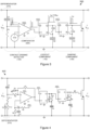
- FIG. 4 is a schematic of a further implementation of a circuit (400) in accordance with the invention.
- Like reference numerals of the circuit (300) of Figure 3 represent like parts in the circuit (400) of Figure 4 .
- a SPICE simulation of the circuit (400) shown in Figure 4 was performed, using the following values for the circuit elements: Table 1: Circuit elements of circuit (400) in Figure 4 Circuit element Value VCC 12V C1 10nF R1.1 2.2k ⁇ R1.2 22k ⁇ D1 6.8V Zener R2 180k ⁇ C2 1 ⁇ P R3 220k ⁇ C3 100nF R5 120k ⁇ R6 1.5k ⁇ C4 100nF R7 10M ⁇ R8 56k ⁇ D2 3.9V Zener D3 1N4007 Silicon diode D4 1N4007 Silicon diode R9 1.5k ⁇ Q1 IRF530 N-channel FET U1 TLC271H opamp U2, U3 CD4013B CMOS Dual
- a PV array of seven PV modules connected in series was used as DC power source. Additional components have been added to the circuit (400) in Figure 4 (as compared to that of Figure 3 ), which doesn't substantially influence the general operation of the circuit, but which may provide better stability and robustness to enable the circuit (400) to perform reliably in the field.
- the overarching requirement is, rather, that the time constants of the two RC circuits are chosen such that the lockout period is sufficiently long to prevent an inadvertent trigger signal being caused by the rising edge of the power supply voltage (V PS ) when the FET (Q1) is removed (i.e. when the near short-circuit is removed).
- D2 which protects the non-inverting input from over-voltage since pulse values exceeding 3.9V will be clamped by the 3.9V Zener diode.
- R7 and R8 provide some hysteresis to the comparator (320) to prevent a false trigger caused by noise.
- D1 has the effect that a negative pulse output from the differentiator (310) will be substantially smaller than a positive. On a positive pulse, the total value of R1 will be the sum of R1.1 and R1.2. On a negative pulse, diode D1 will effectively short-circuit R1.2; and the total value of R1 will only be that of R1.1.
- Voltage divider R5 and R6 provide a reference voltage (V ref ) for the comparator (320), and capacitor C4 provides stability for the reference voltage.
- Diodes D3 and D4 ensure a fast discharge for capacitors C2 and C3.
- the rising edge detector in the embodiments of Figures 3 and 4 are provided by a differentiator and comparator (in an analogue component implementation), it will be appreciated that the functionality of the rising edge detector may also be provided by, for example, a digital implementation with a processor (microprocessor, FPGA, CPLD, and the like), possibly in conjunction with a built-in or external analogue to digital converter.
- the functionality of the rising edge detector may be performed by the processor by sampling the power source output voltage to monitor and detect a rising edge in the power supply output voltage. Upon detection of a rising edge in the power supply output voltage, the processor may then produce a trigger signal to trigger the damping component.
- FIG 5 shows various plots of voltages from the circuit (400) of Figure 4 that has been simulated using SPICE.
- the top-most trace is that of the power supply voltage output (V PS ), which it will be recalled is the same voltage as the load circuit input voltage (V LC ).
- V PS power supply voltage output
- V LC load circuit input voltage
- U1 non-inverting input of the opamp
- V PS The trace of V PS at 90ms corresponds to the scenario at t 0 in Figure 2 , that is when the contact (164) is open and the PV module (150) output voltage (V PS ) is at its open-loop voltage.
- the contact (164) closes, connecting the load (162) into the circuit to draw power from the PV module (150), causing the power supply output voltage V PS to drop from about 250V to about 45V due to the internal resistance of the PV module.
- This causes a negative pulse on the differentiator output which does not cause the comparator (320) to produce a trigger signal, since it does not exceed the reference voltage on the inverting input of the opamp (U1).
- the contact (164) opens, causing a brief rising edge in the power supply voltage (V PS ) and, consequently, a positive pulse is produced by the differentiator (310). This is more clearly shown in Figure 6 , which zooms in on the events at 120ms.
- the output of the opamp (U1) produces a 12V pulse, i.e. the trigger signal.
- the trigger signal causes the output (Q) of the first flip-flop (U2) to produce a 12V pulse for the duration of the lockout period (discussed in more detail below) which, in turn, causes the output (Q) of the second flip-flop (U3) to produce a 12V pulse for the duration of the damping period (DP).
- Figure 7 shows the output (Q) of the second flip-flop (U3) on its bottom trace, and the voltage caused by the RC circuit on the reset input (R) of the second flip-flop on its top trace.
- the capacitor C3 begins to charge and reaches a voltage at about 135ms at which the reset input (R) of the flip-flop (U3) considers the input to be a logic 1.
- This causes the second flip-flop (U3) to be reset and its output (Q) to become a logic 0, i.e. 0V. That, in turn, switches off the FET (Q1) and disconnects the low impedance (or near short-circuit) that had been connected across the power supply input voltage (V PS ) so that this voltage returns to its normal, open-loop voltage.
- FIG. 8 its top trace shows the output voltage (Q) of the first flip-flop (U2) (which forms the lockout component (140)) together with the voltage on its reset pin (R).
- the bottom trace of Figure 8 shows the same for the second flip-flop (U3).
- the time constant of the RC circuit on the reset input (Q) of the first flip-flop (U2) clearly causes its capacitor (C2) to charge much slower, which in turn causes the first flip-flop to be reset much later than the second flip-flop (U3) allowing the lockout period to be considerably longer than the damping period (DP).
- Figure 9 is a schematic of a further circuit (900) in accordance with the invention.
- the component annotations in Figure 9 do not correspond with those in Figures 3 and 4 .
- the topology of the circuit (900) of Figure 9 corresponds largely to that of Figure 4 .
- the differentiator (310) shown in Figure 9 has the same configuration as in Figure 4 , with the resistive part of the RC differentiator comprising two resistors with a Zener diode across the 22k ⁇ resistor.
- the circuit (900) further includes a full bridge diode rectifier (910), which both protects the circuit (900) from reverse polarity connection to the power supply, i.e. the PV module (150), and furthermore enables its proper operation despite a reverse polarity connection. It is worth noting that the load current does not flow through the rectifier (910), but only the current flowing through the FET during the damping period when the FET momentarily causes a near short-circuit across the load circuit.
- the circuit (900) also shows a practical implementation of an internal linear power supply (920) to provide the 12V internal voltage (VCC).
- the circuit (900) also includes an earth fault indicator (930) with two light emitting diodes (LED's) D8 and D9.
- the first LED (D8) is connected between a positive power source connection (940) and an earth connection (942).
- the second LED is connected between the earth connection (942) and a negative power source connection (944). If there is no fault from either the positive connection (940) or the negative connection (944) to the earth connection (942), both LED's illuminate. If the positive connection (940) has an earth fault, the first LED ((D8) will not illuminate; and similarly the second LED (D9) will not illuminate if the negative connection (944) has an earth fault.
- the circuit (900) also includes an FNR-20K681 varistor (MOV1) across the positive power source connection (940) and the negative connection (944) to suppress voltage spikes.
- Figure 10 shows a screenshot of an oscilloscope measurement of the circuit (900) of Figure 9 being powered from a PV array with 7 PV panels (or PV modules) connected in series, and producing an open-loop output voltage of about 226V.
- the power supply voltage is shown by trace (1000) on Figure 10 and is measured with a 10x oscilloscope probe, hence the open-loop voltage appearing to be 22.6V as the measurement is 10 times smaller than the actual measured voltage.
- the second trace (1010) is that of the output (Q) of the second flip-flop (U3), which drives the FET (Q1) to short-circuit the power supply voltage.
- the Applicant has performed experiments with a small relay with a contact rated for switching AC current, to switch DC current from the 7-panel PV array mentioned above to an electric element with an approximate power rating of 1.2kW.
- the relay contact fails catastrophically by burning out as soon as the contacts open while conducting current.
- the same model relay switches without incident and the Applicant has run an endurance test with hundreds of switching cycles with the small relay showing no distress whatsoever.
- Figure 12 is a flow diagram of a method (1200) of enabling a direct current (DC) power source to power a load circuit designed for alternating current (AC) input.
- DC direct current
- AC alternating current
- a DC input voltage is connected (1202) to a load circuit.
- the DC input voltage derived from a DC power source such as the PV module (150) of Figure 1 .
- a switch contact is monitored (1204) to detect an opening event of the contact.
- the contact is connected in series with a load in the load circuit, similarly as shown in Figure 1 .
- the input voltage to the load circuit is momentarily lowered (1208). The momentary lowering of the load circuit input voltage prevents (1210) the sustaining of an electric arc across the opened switch contact.
- the invention therefore provides a circuit and a method enabling a direct current source to power a load circuit designed for alternating current input and, particularly, having a switch contact designed for alternating current, including bi-metallic thermostats, contactors, relays, circuit breakers and toggle switches with contacts rated for AC, to name but a few examples.
Landscapes
- Engineering & Computer Science (AREA)
- Power Engineering (AREA)
- Control Of Voltage And Current In General (AREA)
Claims (15)
- Schaltung (100, 300, 400, 900) mit einem Eingang (102), der zum Verbinden mit einer Gleichstrom-(DC)-Quelle (150) ausgelegt ist, und einem Ausgang (104), der zum Verbinden mit einer Lastschaltung ausgelegt ist, wobei die Lastschaltung (160) eine elektrische Last (162) und einen Schalter mit einem mechanischen Kontakt (164) in Reihe mit der Last enthält, wobei die Schaltung einen Kontaktöffnungsdetektor (120) umfasst, dadurch gekennzeichnet, dass der Öffnungsdetektor (120) zum Erkennen einer ansteigenden Flanke in einer Spannung der Gleichstromquelle am Eingang ausgelegt ist, die ein Öffnungsereignis des Schaltkontakts anzeigt; und eine Dämpfungskomponente (130), die zum Auslösen durch den Kontaktöffnungsdetektor ausgelegt ist, wenn sie ein Kontaktöffnungsereignis erkennt, wobei die ausgelöste Dämpfungskomponente einen momentanen Abfall einer Spannung des Schaltungsausgangs und damit des Lastschaltungseingangs bewirkt, so dass der momentane Abfall der Lastschaltungseingangsspannung die Aufrechterhaltung eines Lichtbogens über den geöffneten Schaltkontakt verhindert.
- Schaltung (100, 300, 400, 900) nach Anspruch 1, wobei die Gleichstromquelle (150) einen solchen Innenwiderstand hat, dass das Schließen von Kontakten des Schaltkontakts einen Abfall der Spannung der Gleichstromquelle bewirkt, wobei das anschließende Öffnen des Schaltkontakts ein erneutes Ansteigen der Spannung der Gleichstromquelle bewirkt, wobei der Kontaktöffnungsdetektor ein Triggersignal erzeugt, wenn die ansteigende Flanke erkannt wird.
- Schaltung (300, 400, 900) nach Anspruch 2, wobei der Kontaktöffnungsdetektor eine Differenziererschaltung (310) enthält; und wobei der Kontaktöffnungsdetektor (120) ferner eine Komparatorkomponente (320) enthält, die zum Produzieren des Triggersignals ausgelegt ist, wenn eine Differenziererausgangsspannung eine Referenzspannung übersteigt.
- Schaltung (100, 300, 400, 900) nach einem der Ansprüche 1 bis 3, wobei die Dämpfungskomponente (130) so ausgelegt ist, dass sie für eine konfigurierte Dämpfungsperiode ausgelöst wird und nach Ablauf der Dämpfungsperiode die Dämpfungskomponente zurücksetzt, wodurch der Abfall der Lastschaltungseingangsspannung rückgängig gemacht wird.
- Schaltung (100, 300, 400, 900) nach Anspruch 4, die ferner eine Sperrkomponente (140) aufweist, ausgelegt zum Verhindern, dass die Dämpfungskomponente (130) für eine Sperrperiode nach dem Auslösen der Dämpfungskomponente erneut ausgelöst wird, wobei die Sperrperiode länger als die Dämpfungsperiode ist, um zu verhindern, dass die Dämpfungskomponente aufgrund einer durch das Zurücksetzen der Dämpfungskomponente verursachten ansteigenden Flanke in der Spannung der Gleichstromquelle (150) ausgelöst wird.
- Schaltung (300, 400, 900) nach Anspruch 5, wobei die Sperrkomponente (140) einen ersten monostabilen Multivibrator umfasst, der zum Auslösen durch das Triggersignal und zum Erzeugen eines der Sperrperiode entsprechenden Ausgangsimpulses ausgelegt ist; undwobei die Dämpfungskomponente einen zweiten monostabilen Multivibrator enthält, der zum Auslösen durch den Ausgangsimpuls des ersten monostabilen Multivibrators und zum Erzeugen eines Ausgangsimpulses entsprechend der Dämpfungsperiode ausgelegt ist, undeinen Dämpfungsschalter, der durch den Ausgangsimpuls des zweiten monostabilen Multivibrators aktiviert wird, wobei der Dämpfungsschalter zum Senken der Lastschaltungseingangsspannung durch Schalten einer niederimpedanten Dämpfungslast parallel zur Lastschaltung wenn aktiviert ausgelegt ist.
- Schaltung (300, 400) nach Anspruch 6, wobei der Dämpfungsschalter ein Halbleiterschalter (Q1) ist, und wobei die Impedanz der Dämpfungslast durch einen Einschaltwiderstand des Halbleiterschalters bereitgestellt wird.
- Schaltung (300, 400) nach Anspruch 6 oder 7, wobei der erste und zweite monostabile Multivibrator jeweils durch ein erstes bzw. ein zweites D-Flipflop (U2, U3) gebildet werden, wobei der Dateneingang des ersten und zweiten Flipflops jeweils mit einem konstanten hohen Eingang verbunden ist, um bei einer ansteigenden Flanke an seinem Takteingang einen hohen Ausgangswert an seinem Ausgangspin zu erzeugen, und eine RC-Schaltung (R2, C2; R3, C3), die mit dem Ausgangspin des Flipflops verbunden und zum Produzieren einer zeitgesteuerten ansteigenden Spannung konfiguriert ist, wenn der Ausgangsstift einen hohen Wert ausgibt, wobei die ansteigende Spannung der RC-Schaltung mit einem Rücksetzpin des Flipflops verbunden ist, um zu bewirken, dass das Flipflop nach einer durch die Zeitkonstante der RC-Schaltung bestimmten Periode zurückgesetzt wird.
- Schaltung (300, 400) nach Anspruch 8, wobei das Triggersignal des Komparators (U1) mit dem Takteingang des ersten Flipflops (U2) verbunden ist, der Ausgang des ersten Flipflops mit dem Takteingang des zweiten Flipflops (U3) verbunden ist und der Ausgang des zweiten Flipflops mit dem Dämpfungsschalter (Q1) verbunden ist; und
wobei die Sperrperiode und die Dämpfungsperiode durch die Zeitkonstante der RC-Schaltung (R2, C2; R3, C3) des ersten bzw. zweiten Flipflops bestimmt wird. - Schaltung (900) nach einem der vorherigen Ansprüche, die ferner einen Vollbrückengleichrichter (910) beinhaltet, um eine Umkehrpolaritätsverbindung der Schaltung mit der Gleichstromquelle zu ermöglichen.
- Schaltung (900) nach einem der vorherigen Ansprüche, die ferner einen Indikator (930) beinhaltet, ausgelegt zum Anzeigen, wenn eine Klemme der Gleichstromquelle elektrischen Strom zu einem Erdanschluss leitet.
- Schaltung (900) nach Anspruch 11, wobei der Indikator (930) eine erste Leuchtdiode (LED) enthält, die zwischen einen positiven Gleichstromquellenanschluss (940) und den Erdanschluss (942) geschaltet ist; und eine zweite Leuchtdiode, die mit dem Erdanschluss (942) und einem negativen Gleichstromquellenanschluss (944) verbunden ist, so dass beide LEDs leuchten, wenn keiner der beiden Gleichstromquellenanschlüsse elektrischen Strom zum Erdanschluss leitet, und so dass nur entweder die erste oder die zweite LED leuchtet, wenn der negative oder positive Gleichstromquellenanschluss elektrischen Strom zum Erdanschluss leiten.
- Verfahren (1200) zum Befähigen einer Gleichstrom-(DC)-Quelle zum Versorgen einer für Wechselstrom-(AC)-Eingang ausgelegten Lastschaltung, das die folgenden Schritte beinhaltet:Verbinden (1202) einer Gleichstromeingangsspannung mit einer Lastschaltung, wobei die Gleichstromeingangsspannung von einer Gleichstromenergiequelle abgeleitet wird;Überwachen (1204) einer Spannung der Gleichstromquelle auf eine ansteigende Flanke, die ein Öffnungsereignis eines Schaltkontakts anzeigt, wobei der Schaltkontakt in Reihe mit einer Last in der Lastschaltung geschaltet ist; undmomentanes Senken (1208), als Reaktion auf das Erkennen (1206) eines Öffnungsereignisses des Kontakts, der Ausgangsspannung der Schaltung und dadurch der Eingangsspannung der Lastschaltung,so dass das momentane Senken derLastschaltungseingangsspannung das Aufrechterhalten eines Lichtbogens über den geöffneten Schaltkontakt verhindert (1210).
- Verfahren nach Anspruch 13, wobei die Gleichstromquelle einen Innenwiderstand hat, so dass das Schließen des Schaltkontakts einen Abfall der Spannung der Gleichstromquelle bewirkt, wobei das anschließende Öffnen des Schaltkontakts ein erneutes Ansteigen der Spannung der Gleichstromquelle bewirkt, wobei ein Triggersignal als Reaktion auf die Erkennung der ansteigenden Flanke produziert wird.
- Verfahren nach Anspruch 13 oder 14, wobei das Erkennen der ansteigenden Flanke in der Spannung der Gleichstromquelle das Produzieren eines zeitabgeleiteten Spannungssignals der Spannung der Gleichstromquelle beinhaltet, und wobei das Erkennen der ansteigenden Flanke in der Spannung der Gleichstromquelle das Vergleichen des zeitabgeleiteten Spannungssignals mit einer Referenzspannung beinhaltet, und wobei das Triggersignal produziert wird, wenn das zeitabgeleitete Spannungssignal die Referenzspannung überschreitet.
Applications Claiming Priority (2)
| Application Number | Priority Date | Filing Date | Title |
|---|---|---|---|
| GB2001707.5A GB2583814B (en) | 2020-02-07 | 2020-02-07 | Method and circuit for enabling a direct current source to power a load circuit designed for alternating current input |
| PCT/IB2021/050542 WO2021156697A1 (en) | 2020-02-07 | 2021-01-25 | Method and circuit for enabling a direct current source to power a load circuit designed for alternating current input |
Publications (3)
| Publication Number | Publication Date |
|---|---|
| EP4100979A1 EP4100979A1 (de) | 2022-12-14 |
| EP4100979B1 true EP4100979B1 (de) | 2023-11-01 |
| EP4100979C0 EP4100979C0 (de) | 2023-11-01 |
Family
ID=69897174
Family Applications (1)
| Application Number | Title | Priority Date | Filing Date |
|---|---|---|---|
| EP21702718.4A Active EP4100979B1 (de) | 2020-02-07 | 2021-01-25 | Verfahren und schaltung zur ermöglichung einer gleichstromquelle zur speisung eines lastkreises mit wechselstromeingang |
Country Status (5)
| Country | Link |
|---|---|
| US (1) | US12112914B2 (de) |
| EP (1) | EP4100979B1 (de) |
| GB (1) | GB2583814B (de) |
| WO (1) | WO2021156697A1 (de) |
| ZA (1) | ZA202208516B (de) |
Families Citing this family (1)
| Publication number | Priority date | Publication date | Assignee | Title |
|---|---|---|---|---|
| GB2583814B (en) | 2020-02-07 | 2021-05-12 | Poweroptimal Pty Ltd | Method and circuit for enabling a direct current source to power a load circuit designed for alternating current input |
Family Cites Families (7)
| Publication number | Priority date | Publication date | Assignee | Title |
|---|---|---|---|---|
| JP5582007B2 (ja) * | 2009-12-18 | 2014-09-03 | 東芝ライテック株式会社 | 直流電力スイッチ装置 |
| DE202012100023U1 (de) * | 2012-01-04 | 2012-04-12 | Abb Technology Ag | HVDC-Hybrid-Leistungsschalter mit Schutzbeschaltung |
| JP5943484B2 (ja) * | 2013-05-07 | 2016-07-05 | シオン電機株式会社 | 直流電源使用時に生ずるアーク放電防止システム |
| US9726725B2 (en) * | 2013-08-02 | 2017-08-08 | Jtekt Corporation | Power circuit abnormality detection method |
| US9991075B2 (en) * | 2013-10-04 | 2018-06-05 | Lutron Electronics Co., Inc. | Controlling a controllably conductive device based on zero-crossing detection |
| PT3210226T (pt) * | 2014-10-24 | 2019-07-25 | Ellenberger & Poensgen | Disjuntor para interrupção de corrente contínua galvânica |
| GB2583814B (en) | 2020-02-07 | 2021-05-12 | Poweroptimal Pty Ltd | Method and circuit for enabling a direct current source to power a load circuit designed for alternating current input |
-
2020
- 2020-02-07 GB GB2001707.5A patent/GB2583814B/en active Active
-
2021
- 2021-01-25 WO PCT/IB2021/050542 patent/WO2021156697A1/en not_active Ceased
- 2021-01-25 US US17/797,977 patent/US12112914B2/en active Active
- 2021-01-25 EP EP21702718.4A patent/EP4100979B1/de active Active
-
2022
- 2022-07-29 ZA ZA2022/08516A patent/ZA202208516B/en unknown
Also Published As
| Publication number | Publication date |
|---|---|
| US20230068037A1 (en) | 2023-03-02 |
| EP4100979C0 (de) | 2023-11-01 |
| GB2583814B (en) | 2021-05-12 |
| US12112914B2 (en) | 2024-10-08 |
| GB202001707D0 (en) | 2020-03-25 |
| WO2021156697A1 (en) | 2021-08-12 |
| ZA202208516B (en) | 2023-01-25 |
| GB2583814A (en) | 2020-11-11 |
| EP4100979A1 (de) | 2022-12-14 |
Similar Documents
| Publication | Publication Date | Title |
|---|---|---|
| CN101868898B (zh) | 在调光器电路中的过电流状态检测方法、检测电路及调光器电路 | |
| CN106169925B (zh) | 具有输出均流的单片集成电路开关器件 | |
| CN115461629A (zh) | 智能电路中断 | |
| CA2639864C (en) | Circuit interrupter | |
| CN109245053A (zh) | 一种过载保护电路 | |
| CN103208782A (zh) | 一种工频和变频电源的综合检测和用电保护装置 | |
| US20180019584A1 (en) | Leakage current detection and protection device | |
| CN104836196A (zh) | 一种延时启动的过流保护电路 | |
| EP4100979B1 (de) | Verfahren und schaltung zur ermöglichung einer gleichstromquelle zur speisung eines lastkreises mit wechselstromeingang | |
| CN210468780U (zh) | 继电器式漏电保护装置、电连接设备以及用电器 | |
| CN203645292U (zh) | 过压过流保护电路 | |
| CN207440181U (zh) | 一种高压断路器动态电阻测量系统 | |
| CN110416009B (zh) | 无电弧长寿命的继电器开关电路及控制器 | |
| CN101562092B (zh) | 过零动作磁保持继电器 | |
| CN211127104U (zh) | 断路器 | |
| Kumar et al. | Surge immunity protection in AC LED Street Lights | |
| CN208753971U (zh) | 一种过载保护电路 | |
| Vasavada et al. | Development of Intelligent Automatic Electronic MCB and ELCB Using Fault Diagnosis Technique | |
| CN111756016A (zh) | 一种继电器 | |
| CN214703795U (zh) | 一种三相电压相序记忆及报警装置 | |
| CN2785226Y (zh) | 远距离相间短路保护器 | |
| CN110265966A (zh) | 过载和短路保护电路 | |
| WO1995023455A1 (en) | Switching device for telecommunications channel | |
| CN2842833Y (zh) | 单相电子式漏电保护开关 | |
| Zhang et al. | Research on Overvoltage Detection Method of Flyback Switching Power Module Based on Time Relay |
Legal Events
| Date | Code | Title | Description |
|---|---|---|---|
| STAA | Information on the status of an ep patent application or granted ep patent |
Free format text: STATUS: UNKNOWN |
|
| STAA | Information on the status of an ep patent application or granted ep patent |
Free format text: STATUS: THE INTERNATIONAL PUBLICATION HAS BEEN MADE |
|
| PUAI | Public reference made under article 153(3) epc to a published international application that has entered the european phase |
Free format text: ORIGINAL CODE: 0009012 |
|
| STAA | Information on the status of an ep patent application or granted ep patent |
Free format text: STATUS: REQUEST FOR EXAMINATION WAS MADE |
|
| 17P | Request for examination filed |
Effective date: 20220803 |
|
| AK | Designated contracting states |
Kind code of ref document: A1 Designated state(s): AL AT BE BG CH CY CZ DE DK EE ES FI FR GB GR HR HU IE IS IT LI LT LU LV MC MK MT NL NO PL PT RO RS SE SI SK SM TR |
|
| DAV | Request for validation of the european patent (deleted) | ||
| DAX | Request for extension of the european patent (deleted) | ||
| GRAP | Despatch of communication of intention to grant a patent |
Free format text: ORIGINAL CODE: EPIDOSNIGR1 |
|
| STAA | Information on the status of an ep patent application or granted ep patent |
Free format text: STATUS: GRANT OF PATENT IS INTENDED |
|
| INTG | Intention to grant announced |
Effective date: 20230531 |
|
| GRAS | Grant fee paid |
Free format text: ORIGINAL CODE: EPIDOSNIGR3 |
|
| GRAA | (expected) grant |
Free format text: ORIGINAL CODE: 0009210 |
|
| STAA | Information on the status of an ep patent application or granted ep patent |
Free format text: STATUS: THE PATENT HAS BEEN GRANTED |
|
| AK | Designated contracting states |
Kind code of ref document: B1 Designated state(s): AL AT BE BG CH CY CZ DE DK EE ES FI FR GR HR HU IE IS IT LI LT LU LV MC MK MT NL NO PL PT RO RS SE SI SK SM TR |
|
| RBV | Designated contracting states (corrected) |
Designated state(s): AL AT BE BG CH CY CZ DE DK EE ES FI FR GR HR HU IE IS IT LI LT LU LV MC MK MT NL NO PL PT RO RS SE SI SK SM TR |
|
| REG | Reference to a national code |
Ref country code: CH Ref legal event code: EP |
|
| REG | Reference to a national code |
Ref country code: IE Ref legal event code: FG4D |
|
| REG | Reference to a national code |
Ref country code: DE Ref legal event code: R096 Ref document number: 602021006444 Country of ref document: DE |
|
| U01 | Request for unitary effect filed |
Effective date: 20231128 |
|
| U07 | Unitary effect registered |
Designated state(s): AT BE BG DE DK EE FI FR IT LT LU LV MT NL PT SE SI Effective date: 20231205 |
|
| U20 | Renewal fee for the european patent with unitary effect paid |
Year of fee payment: 4 Effective date: 20231228 |
|
| PG25 | Lapsed in a contracting state [announced via postgrant information from national office to epo] |
Ref country code: GR Free format text: LAPSE BECAUSE OF FAILURE TO SUBMIT A TRANSLATION OF THE DESCRIPTION OR TO PAY THE FEE WITHIN THE PRESCRIBED TIME-LIMIT Effective date: 20240202 |
|
| PG25 | Lapsed in a contracting state [announced via postgrant information from national office to epo] |
Ref country code: IS Free format text: LAPSE BECAUSE OF FAILURE TO SUBMIT A TRANSLATION OF THE DESCRIPTION OR TO PAY THE FEE WITHIN THE PRESCRIBED TIME-LIMIT Effective date: 20240301 |
|
| PG25 | Lapsed in a contracting state [announced via postgrant information from national office to epo] |
Ref country code: ES Free format text: LAPSE BECAUSE OF FAILURE TO SUBMIT A TRANSLATION OF THE DESCRIPTION OR TO PAY THE FEE WITHIN THE PRESCRIBED TIME-LIMIT Effective date: 20231101 |
|
| PG25 | Lapsed in a contracting state [announced via postgrant information from national office to epo] |
Ref country code: IS Free format text: LAPSE BECAUSE OF FAILURE TO SUBMIT A TRANSLATION OF THE DESCRIPTION OR TO PAY THE FEE WITHIN THE PRESCRIBED TIME-LIMIT Effective date: 20240301 Ref country code: GR Free format text: LAPSE BECAUSE OF FAILURE TO SUBMIT A TRANSLATION OF THE DESCRIPTION OR TO PAY THE FEE WITHIN THE PRESCRIBED TIME-LIMIT Effective date: 20240202 Ref country code: ES Free format text: LAPSE BECAUSE OF FAILURE TO SUBMIT A TRANSLATION OF THE DESCRIPTION OR TO PAY THE FEE WITHIN THE PRESCRIBED TIME-LIMIT Effective date: 20231101 |
|
| PG25 | Lapsed in a contracting state [announced via postgrant information from national office to epo] |
Ref country code: RS Free format text: LAPSE BECAUSE OF FAILURE TO SUBMIT A TRANSLATION OF THE DESCRIPTION OR TO PAY THE FEE WITHIN THE PRESCRIBED TIME-LIMIT Effective date: 20231101 Ref country code: PL Free format text: LAPSE BECAUSE OF FAILURE TO SUBMIT A TRANSLATION OF THE DESCRIPTION OR TO PAY THE FEE WITHIN THE PRESCRIBED TIME-LIMIT Effective date: 20231101 Ref country code: NO Free format text: LAPSE BECAUSE OF FAILURE TO SUBMIT A TRANSLATION OF THE DESCRIPTION OR TO PAY THE FEE WITHIN THE PRESCRIBED TIME-LIMIT Effective date: 20240201 Ref country code: HR Free format text: LAPSE BECAUSE OF FAILURE TO SUBMIT A TRANSLATION OF THE DESCRIPTION OR TO PAY THE FEE WITHIN THE PRESCRIBED TIME-LIMIT Effective date: 20231101 |
|
| PG25 | Lapsed in a contracting state [announced via postgrant information from national office to epo] |
Ref country code: CZ Free format text: LAPSE BECAUSE OF FAILURE TO SUBMIT A TRANSLATION OF THE DESCRIPTION OR TO PAY THE FEE WITHIN THE PRESCRIBED TIME-LIMIT Effective date: 20231101 |
|
| PG25 | Lapsed in a contracting state [announced via postgrant information from national office to epo] |
Ref country code: SK Free format text: LAPSE BECAUSE OF FAILURE TO SUBMIT A TRANSLATION OF THE DESCRIPTION OR TO PAY THE FEE WITHIN THE PRESCRIBED TIME-LIMIT Effective date: 20231101 |
|
| PG25 | Lapsed in a contracting state [announced via postgrant information from national office to epo] |
Ref country code: SM Free format text: LAPSE BECAUSE OF FAILURE TO SUBMIT A TRANSLATION OF THE DESCRIPTION OR TO PAY THE FEE WITHIN THE PRESCRIBED TIME-LIMIT Effective date: 20231101 Ref country code: SK Free format text: LAPSE BECAUSE OF FAILURE TO SUBMIT A TRANSLATION OF THE DESCRIPTION OR TO PAY THE FEE WITHIN THE PRESCRIBED TIME-LIMIT Effective date: 20231101 Ref country code: CZ Free format text: LAPSE BECAUSE OF FAILURE TO SUBMIT A TRANSLATION OF THE DESCRIPTION OR TO PAY THE FEE WITHIN THE PRESCRIBED TIME-LIMIT Effective date: 20231101 |
|
| REG | Reference to a national code |
Ref country code: DE Ref legal event code: R097 Ref document number: 602021006444 Country of ref document: DE |
|
| PG25 | Lapsed in a contracting state [announced via postgrant information from national office to epo] |
Ref country code: MC Free format text: LAPSE BECAUSE OF FAILURE TO SUBMIT A TRANSLATION OF THE DESCRIPTION OR TO PAY THE FEE WITHIN THE PRESCRIBED TIME-LIMIT Effective date: 20231101 |
|
| U1N | Appointed representative for the unitary patent procedure changed after the registration of the unitary effect |
Representative=s name: REDDIE & GROSE LLP; GB |
|
| PG25 | Lapsed in a contracting state [announced via postgrant information from national office to epo] |
Ref country code: MC Free format text: LAPSE BECAUSE OF FAILURE TO SUBMIT A TRANSLATION OF THE DESCRIPTION OR TO PAY THE FEE WITHIN THE PRESCRIBED TIME-LIMIT Effective date: 20231101 |
|
| REG | Reference to a national code |
Ref country code: CH Ref legal event code: PL |
|
| PLBE | No opposition filed within time limit |
Free format text: ORIGINAL CODE: 0009261 |
|
| STAA | Information on the status of an ep patent application or granted ep patent |
Free format text: STATUS: NO OPPOSITION FILED WITHIN TIME LIMIT |
|
| 26N | No opposition filed |
Effective date: 20240802 |
|
| PG25 | Lapsed in a contracting state [announced via postgrant information from national office to epo] |
Ref country code: CH Free format text: LAPSE BECAUSE OF NON-PAYMENT OF DUE FEES Effective date: 20240131 |
|
| PG25 | Lapsed in a contracting state [announced via postgrant information from national office to epo] |
Ref country code: CH Free format text: LAPSE BECAUSE OF NON-PAYMENT OF DUE FEES Effective date: 20240131 |
|
| U20 | Renewal fee for the european patent with unitary effect paid |
Year of fee payment: 5 Effective date: 20241118 |
|
| PG25 | Lapsed in a contracting state [announced via postgrant information from national office to epo] |
Ref country code: IE Free format text: LAPSE BECAUSE OF NON-PAYMENT OF DUE FEES Effective date: 20240125 |
|
| PG25 | Lapsed in a contracting state [announced via postgrant information from national office to epo] |
Ref country code: IE Free format text: LAPSE BECAUSE OF NON-PAYMENT OF DUE FEES Effective date: 20240125 |
|
| PG25 | Lapsed in a contracting state [announced via postgrant information from national office to epo] |
Ref country code: RO Free format text: LAPSE BECAUSE OF FAILURE TO SUBMIT A TRANSLATION OF THE DESCRIPTION OR TO PAY THE FEE WITHIN THE PRESCRIBED TIME-LIMIT Effective date: 20231101 |
|
| PG25 | Lapsed in a contracting state [announced via postgrant information from national office to epo] |
Ref country code: CY Free format text: LAPSE BECAUSE OF FAILURE TO SUBMIT A TRANSLATION OF THE DESCRIPTION OR TO PAY THE FEE WITHIN THE PRESCRIBED TIME-LIMIT; INVALID AB INITIO Effective date: 20210125 |
|
| PG25 | Lapsed in a contracting state [announced via postgrant information from national office to epo] |
Ref country code: HU Free format text: LAPSE BECAUSE OF FAILURE TO SUBMIT A TRANSLATION OF THE DESCRIPTION OR TO PAY THE FEE WITHIN THE PRESCRIBED TIME-LIMIT; INVALID AB INITIO Effective date: 20210125 |
|
| PG25 | Lapsed in a contracting state [announced via postgrant information from national office to epo] |
Ref country code: TR Free format text: LAPSE BECAUSE OF FAILURE TO SUBMIT A TRANSLATION OF THE DESCRIPTION OR TO PAY THE FEE WITHIN THE PRESCRIBED TIME-LIMIT Effective date: 20231101 |
|
| U20 | Renewal fee for the european patent with unitary effect paid |
Year of fee payment: 6 Effective date: 20260126 |