EP4094331B1 - Agencement de commutation électrique - Google Patents
Agencement de commutation électrique Download PDFInfo
- Publication number
- EP4094331B1 EP4094331B1 EP21702079.1A EP21702079A EP4094331B1 EP 4094331 B1 EP4094331 B1 EP 4094331B1 EP 21702079 A EP21702079 A EP 21702079A EP 4094331 B1 EP4094331 B1 EP 4094331B1
- Authority
- EP
- European Patent Office
- Prior art keywords
- insulation
- switching arrangement
- electrical switching
- electrodes
- insulation block
- Prior art date
- Legal status (The legal status is an assumption and is not a legal conclusion. Google has not performed a legal analysis and makes no representation as to the accuracy of the status listed.)
- Active
Links
Images

Classifications
-
- H—ELECTRICITY
- H01—ELECTRIC ELEMENTS
- H01T—SPARK GAPS; OVERVOLTAGE ARRESTERS USING SPARK GAPS; SPARKING PLUGS; CORONA DEVICES; GENERATING IONS TO BE INTRODUCED INTO NON-ENCLOSED GASES
- H01T2/00—Spark gaps comprising auxiliary triggering means
- H01T2/02—Spark gaps comprising auxiliary triggering means comprising a trigger electrode or an auxiliary spark gap
-
- H—ELECTRICITY
- H01—ELECTRIC ELEMENTS
- H01T—SPARK GAPS; OVERVOLTAGE ARRESTERS USING SPARK GAPS; SPARKING PLUGS; CORONA DEVICES; GENERATING IONS TO BE INTRODUCED INTO NON-ENCLOSED GASES
- H01T4/00—Overvoltage arresters using spark gaps
- H01T4/10—Overvoltage arresters using spark gaps having a single gap or a plurality of gaps in parallel
-
- H—ELECTRICITY
- H01—ELECTRIC ELEMENTS
- H01T—SPARK GAPS; OVERVOLTAGE ARRESTERS USING SPARK GAPS; SPARKING PLUGS; CORONA DEVICES; GENERATING IONS TO BE INTRODUCED INTO NON-ENCLOSED GASES
- H01T4/00—Overvoltage arresters using spark gaps
- H01T4/16—Overvoltage arresters using spark gaps having a plurality of gaps arranged in series
Definitions
- This invention relates to an electrical switching arrangement, in particular to an electrical switching arrangement for discharging a high voltage from a capacitor.
- a switching device such as a spark gap may be used.
- An example of a spark gap is shown in GB 2 438 530 A .
- an insulating spacer may be provided between the electrodes of the switch and between the different terminals (e.g. live and ground) of the high voltage system.
- the voltages used are particularly high (e.g. > 80 kV)
- the amount of dielectric material (e.g. of the insulating spacer) provided is therefore a trade-off between the ability of the switching device to switch a high voltage rapidly and its ability to prevent dielectric breakdown at a high voltage.
- US 4 092 559 A discloses an electrical switching arrangement according to the preamble of claim 1 and describes a low inductance controlled discharger for commutating megampere currents, having a maximum controllability range with respect to voltage, and a small operation lag.
- CA 654 914 A describes high current, low inductance arc discharge switches of the magnetohydrodynamic type.
- An aim of the present invention is provide an improved electrical switching arrangement.
- the invention provides an electrical switching arrangement for an electrical power supply, the electrical switching arrangement comprising:
- the present invention provides an electrical switching arrangement for an electrical power supply, e.g. for switching between (connecting) a voltage source and a load.
- the switching arrangement includes a live conductor and a ground conductor.
- the live conductor includes a set of electrodes for switching between first and second sides of the live conductor, e.g. for switching between (connecting) the voltage source and the load.
- the set of electrodes are provided between the first and second sides of the live conductor.
- An insulation block (e.g. a backing plate) is positioned between the live conductor and the ground conductor, at the location of the set of electrodes.
- the insulation block includes two grooves in which two insulation members are located respectively. The insulation members extend from the insulation block on either side of the live conductor.
- the arrangement of the present invention also helps to reduce the inductance of the electrical switching arrangement, owing to the insulation members fitting into the respective grooves of the insulation block. This is because the grooves, with part of the insulation members located therein, help to reduce the risk of surface tracking across the face of the insulation block adjacent to the ground conductor, by acting as a trap for any surface tracking (it should be noted that in at least preferred embodiments the risk of dielectric breakdown directly across the set of electrodes is relatively low owing to the spacing of the electrodes and/or resistance in the switching arrangement). This may therefore allow the live conductor and the ground conductor to be brought closer together owing to not having to provide a (e.g. single) large insulation block for the purposes of reducing the risk of surface tracking, thus reducing the inductance.
- the insulation members extending outwards from the insulation block on both sides of the live conductor (and thus also for the opposing ground conductor), also help to reduce the risk of dielectric breakdown between the live conductor and the ground conductor, e.g. on the first side of the live conductor when a voltage source is being used to charge the live conductor over a period of time to a high voltage.
- the electrical switching arrangement may be used with any suitable and desired power supply.
- the electrical switching arrangement is arranged to connect (and thus switch between) a voltage source and a load.
- the voltage source preferably comprises (e.g. an array of) one or more capacitors, arranged to be charged to store a charge at a voltage.
- the one or more capacitors are connected to the electrical switching arrangement and arranged to discharge a voltage through the electrical switching arrangement.
- the live conductor of the electrical switching arrangement is connected to the live terminal of the voltage source (e.g. of the capacitor).
- the live conductor of the electrical switching arrangement is connected to a live output terminal (e.g. plate) of (e.g. a capacitor header) of a capacitor.
- the first side of the live conductor may, for example, comprise (or be an extension of) a live output terminal (e.g. a live output plate) of a capacitor.
- the live conductor, live terminal and the live output terminal (as well as any other live components connected thereto) may be at either a positive or a negative voltage relative to the respective ground components of the switching arrangement.
- the ground conductor of the electrical switching arrangement is connected to a ground output terminal of the voltage source, e.g. to a ground output terminal (e.g. plate) of (e.g. a capacitor header) of a (e.g. same or different) capacitor.
- the first side of the ground conductor may, for example, comprise (or be an extension of) a ground output terminal (e.g. a ground output plate) of a capacitor.
- the invention extends to the electrical power supply per se and thus when viewed from a further aspect the invention provides an electrical power supply for supplying an output voltage to a load, the electrical power supply comprising:
- this aspect of the invention may (and preferably does) include one or more (e.g. all) of the preferred and optional features outlined herein.
- the (e.g. voltage source of the) electrical power supply may be arranged to generate, and the electrical switching arrangement may be arranged to switch, any suitable and desired voltage and/or current, e.g. to a load.
- the electrical power supply is arranged to generate, and the electrical switching arrangement is arranged to switch, a voltage of at least 30 kV, e.g. at least 50 kV, e.g. approximately 60 kV.
- the electrical switching arrangement and the electrical power supply may be used to switch and supply an output voltage for any suitable and desired use, e.g. to a load.
- the electrical switching arrangement is used to connect (i.e. conduct) the two sides of the live conductor, e.g. to discharge a voltage from (e.g. a voltage source on) the first side of the live conductor to the second side of the live conductor, e.g. to deliver the voltage to a load.
- the electrical switching arrangement and the electrical power supply is used to deliver a high voltage and current pulse to a load in a vacuum chamber, e.g. as part of a pulsed power system.
- electrical switching arrangement and the electrical power supply may be used in any (e.g. high) voltage power system in which the terminals (conductors) are spatially close and likely to have a large voltage difference across them. This may include, for example, electricity mains switches for power applications that desire lower inductance and a compact high voltage switch design.
- the live conductor and the ground conductor may have any suitable and desired geometry.
- the live conductor comprises a live conducting plate and the ground conductor comprises a ground conducting plate.
- the live conducting plate and the ground conducting plate are (e.g. extended) substantially parallel to each other, e.g. with the insulation block and the first and second insulation members lying between the conducting plates.
- the live conductor and the ground conductor may be formed from any suitable and desired (e.g. conductive) material.
- the live conductor and/or the ground conductor are formed from metal, e.g. aluminium.
- the live conductor has a first side and a second side.
- the live conductor extends on each side of the set of electrodes (and thus of the electrical switching arrangement).
- one or each side of the live conductor comprises a live conducting plate.
- the ground conductor extends (e.g. continuously) through (and, e.g., on both sides of) the set of electrodes (and thus of the electrical switching arrangement).
- the set of electrodes for switching between (i.e. providing a conducting connection) the first and second sides of the live conductor, may be provided in any suitable and desired way.
- the set of electrodes comprises a spark (e.g. ball) gap.
- the set of electrodes comprises an array of spark ball gaps (e.g. a multi-channel ball gap switch), e.g. extending between the first and second sides of the live conductor and/or extending along the first and second sides of the live conductor.
- the electrical switching arrangement comprises a trigger arranged to initiate the switching of (e.g. conducting across) the set of electrodes.
- the trigger is arranged to perturb the electric field within the electrical switching arrangement, which causes an electrical breakdown to cascade, thus completing an electric circuit through the set of electrodes.
- the insulation block between the set of electrodes and the ground conductor may be provided in any suitable and desired way.
- the insulation block extends across (and, e.g., beyond) the set of electrodes between the first and second sides of the live conductor.
- the insulation block has a thickness (in the direction between the set of electrodes and the ground conductor) that is less than a length (in the direction across the set of electrodes) and/or a width (in the direction perpendicular to the thickness and the length) of the insulation block.
- the insulation block is substantially planar.
- the insulation block preferably has a length of between 30 cm and 50 cm, e.g. between 35 cm and 45 cm, e.g. approximately 40 cm.
- the insulation block preferably has a width of between 20 cm and 40 cm, e.g. between 25 cm and 35 cm, e.g. approximately 30 cm.
- the insulation block has a length and/or a width greater than or equal to the corresponding dimension(s) of the set of electrodes.
- the insulation block may be substantially cuboid; however, in a set of embodiments the edges of the insulation block (e.g. on the first and second sides of the live conductor) are tapered in a direction towards the respective edges, e.g. between the grooves and the respective edges of the insulation block where the insulation members overlap with the insulation block.
- the tapering of the insulation block may help to reduce the inductance of the electrical switching arrangement.
- the insulation block has a thickness at an edge of the insulation block proximal to the first side of the set of electrodes (which, e.g., is connected to a voltage source and thus in use is charged to a high voltage) that is greater than a thickness at an edge of the insulation block proximal to the second side of the set of electrodes.
- the thickness of the insulation block increases across the insulation block in a direction parallel to the direction from the second side of the set of electrodes to the first set of electrodes.
- the insulation block is substantially wedge-shaped, e.g. having a substantially triangular cross-section (e.g. in a plane perpendicular to the width of the insulation block).
- the insulation block may be formed from any suitable and desired dielectric material.
- the insulation block comprises a solid (e.g. substantially incompressible, e.g. rigid) block.
- the insulation block is formed from plastic, e.g. a thermoplastic.
- the insulation block member is formed from polyethylene (PE). PE has a relatively high stiffness and dielectric strength, and a good dimensional stability. This helps to provide good insulation and structural integrity in the electrical switching arrangement, particularly when a high voltage is switched through the electrical switching arrangement.
- the first and second insulation members may be formed in any suitable and desired way to extend from, and to fit in the respective grooves of, the insulation block.
- the first and second insulation members may each be formed from a solid (e.g. substantially rigid) block of material (e.g. made from the same material as the insulation block) that is shaped (e.g. with an angle at the edge of the block of material) to fit into the respective groove in the insulation block.
- the first and second insulation members e.g. in a similar manner to the insulation block, may be substantially planar (e.g. apart from the edge that fits into the groove), e.g. having a thickness between 1 mm and 2 mm.
- the first and second insulation members comprise a first set of one or more insulation sheets and a second set of one or more insulation sheets.
- Providing (e.g. flexible) sheets of insulation both helps to fit the sheets into the respective grooves of the insulation block and to reduce the thickness of the combined insulation block and insulation sheets, thus reducing the inductance of the electrical switching arrangement.
- the first and second sets of one or more insulation sheets may be inserted into and secured in the respective grooves of the insulation member in any suitable and desired way.
- the insulation sheet(s) are folded and tucked into the respective grooves. Having the insulation sheet(s) folding back on itself, against the electric field gradient, helps to prevent charge from migrating to and around the insulation block, thus helping to reduce the risk of surface tracking.
- the insulation sheet(s) are secured in the respective grooves by adhesive tape.
- the first and second grooves in the insulation block may be shaped and sized in any suitable and desired way for receiving the respective insulation members.
- the grooves are formed in the side of the insulation block facing the ground conductor (i.e. opposite the set of electrodes and the live conductor).
- the grooves are formed towards the respective edges (e.g. closer to the edge than the centre) of the insulation block (e.g. the edges in the directions in which the first and second sides of the live conductor extend respectively).
- the grooves extend (e.g. substantially all the way across the insulation block) in a direction perpendicular to the directions in which the first and second sides of the live conductor extend from the set of electrodes. This helps to reduce the risk of any surface tracking occurring as the grooves extend perpendicularly to the direction in which surface tracking may occur.
- the grooves are aligned with the respective edges of the sides of the live conductor, proximal to the set of electrodes.
- the set of electrodes comprises an array of spark ball gaps
- the grooves are aligned with the row of balls closest to the respective side of the live conductor.
- the grooves may extend into the insulation block at any suitable and desired angle.
- the first groove extends into the insulation block at an angle of less than 90 degrees to the face of the insulation block in the direction in which the first insulation member extends from the (e.g. opening of the) first groove.
- the second groove extends into the insulation block at an angle of less than 90 degrees to the face of the insulation block in the direction in which the second insulation member extends from the (e.g. opening of the) second groove. Having the grooves extend at an acute angle means that the insulation members turn back on themselves into the respective grooves, against the electric field gradient, thus helping to prevent charge from migrating along the insulation block. This helps to reduce the risk of surface tracking owing to the increased electric field gradient.
- the grooves may extend into the insulation block to any suitable and desired depth.
- the grooves extend at least 10 mm, e.g. at least 12 mm, into the insulation block.
- the grooves may have any suitable and desired width (in a direction perpendicular to the directions in which the grooves extend across and into the insulation block), e.g. depending on the nature (e.g. solid or sheets) of the insulation members.
- the grooves across the full width of the insulation block. This allows the insulation members to extend across (and, e.g., beyond) the width of the insulation block.
- the insulation members extend (e.g. in a direction parallel to the direction in which the grooves extend) beyond the insulation block.
- the first and second insulation members may extend by any suitable and desired distance from the insulation block.
- the first insulation member preferably extends for a distance from the insulation block that is greater than or equal to the distance that the first side of live conductor extends from the set of electrodes.
- the first insulation member preferably extends for a distance from the insulation block that is greater than or equal to the distance that the ground conductor extends from the (e.g. first groove in the) insulation block in a direction parallel to the direction in which the first side of live conductor extends from the set of electrodes.
- the second insulation member preferably extends for a distance from the insulation block that is greater than or equal to the distance that the second side of live conductor extends from the set of electrodes.
- the second insulation member preferably extends for a distance from the insulation block that is greater than or equal to the distance that the ground conductor extends from the (e.g. second groove in the) insulation block in a direction parallel to the direction in which the second side of live conductor extends from the set of electrodes.
- the insulation members extending at least as far as the sides of the live conductor and/or at least as far as the ground conductor helps to increase the path length between the two sides of the live conductor around the insulation members, and between the live conductor and the ground conductor around the insulation members, to reduce the risk of surface tracking between the two sides of the live conductor and between the live conductor and the ground conductor.
- the first and second sets of insulating sheet(s) may each comprise only a single insulating sheet.
- the first and/or second sets of insulating sheets (e.g. each) comprises a plurality of insulating sheets (i.e. the first set of insulating sheets may have multiple sheets therein and/or the second set of insulating sheets may have multiple sheets therein).
- the plurality of insulation sheets in (e.g. each) of the first and/or second sets of insulation sheets preferably comprises at least four insulation sheets, e.g. at least six insulation sheets, e.g. approximately eight insulation sheets.
- the number of sheets in each set may depend on the working voltage, the thickness of the insulating members and/or the dielectric strength of the insulating members.
- Providing multiple sheets in each set of insulation sheets helps to increase the amount of insulation, which helps to reduce the risk of electrical punch-through between the live conductor and the ground conductor, e.g. for an electric field gradient of greater than 150 MV/m, and to help to reduce the risk surface tracking across the insulation member.
- the first and second sets of insulating sheet(s) may have any suitable and desired geometry.
- each of the one or more insulating sheets in the first and second sets of insulating sheet(s) have a thickness (e.g. in a direction between the live conductor and the ground output conductor) less than 200 microns, e.g. less than 100 microns, e.g. approximately 75 microns.
- the Applicant has appreciated that a larger number of thinner insulation sheets helps to offer greater protection against electrical breakdown, while having little effect on the separation of the live conductor and the ground conductor.
- the first and second sets of insulating sheet(s) may be made from any suitable and desired (dielectric) material, e.g. a thin film.
- the first and second sets of insulating sheet(s) are made from a polyester, e.g. biaxially-oriented polyethylene terephthalate (boPET) such as Mylar (RTM).
- BoPET biaxially-oriented polyethylene terephthalate
- RTM Mylar
- Such a stretched thin film has a relatively high dielectric strength (thus providing a greater resistance to dielectric breakdown when subject to a high electric field) and is relatively durable and pliable (making it suitable for being manipulated when assembling the electrical switching arrangement, particularly for fitting into the grooves of the insulation block).
- Switching arrangements are important components in high voltage systems, e.g. when discharging a high voltage from a capacitor to deliver a high voltage pulse to a load.
- Embodiments of an electrical power supply and an electrical switching arrangement in accordance with the present invention will now be described.
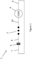
- FIG. 1 shows schematically an electrical power supply system 1 for supplying a high voltage pulse generated by a capacitor 4 to a load 6 through an electrical switching arrangement 2 in accordance with an embodiment of the present invention.
- the capacitor 4 (or array of capacitors) is connected to the electrical switching arrangement 2 (which comprises an array of spark ball gaps) by a first live conductor 8 and ground conductor 7.
- the load 6 is connected to the electrical switching arrangement 2 by a second live conductor 10 and ground conductor 9.
- FIG. 2 shows schematically a cross-section of an electrical switching arrangement 11 in accordance with an embodiment of the present invention.
- the electrical switching arrangement 11 comprises an array of spark ball gaps 12 that connect a first side 14 and a second side 16 of a live conductor plate.
- the electrical switching arrangement 11 comprises a trigger 13 for triggering switching of the electrical switching arrangement 11.
- the first side of the live conductor plate 14 connects the spark ball gaps 12 to the live output of a capacitor.
- the second side of the live conductor plate 16 connects the spark ball gaps 12 to a load.
- the electrical switching arrangement 11 also comprises a ground conductor plate 18 that extends across the electrical switching arrangement 11 between the capacitor and the load.
- the ground conductor plate 18 lies parallel to the first and second sides of the live conductor plate 14, 16.
- the solid insulation block 20 is generally planar with tapered edges and two grooves 22, 24 formed in the side of the solid insulation block 20 that faces the ground conductor plate 18.
- the grooves 22, 24 extend into the thickness of the solid insulation block 20 at an acute angle and extend across the width of the solid insulation block 20, aligned with the sets of spark balls at the edges of the array of spark ball gaps 12.
- a first set of eight 75 micron Mylar (RTM) insulation sheets 26 is folded into the first groove 22 of the insulation block 20.
- the first set of insulation sheets 26 extends from the first groove 22 along the surface of the insulation block 20 to and beyond the tapered edge of the insulation block 20.
- the first set of insulation sheets 26 extends from the edge of the ground conductor plate 18.
- a second set of eight 75 micron Mylar (RTM) insulation sheets 28 is folded into the second groove 24 of the insulation block 20.
- the second set of insulation sheets 28 extends from the second groove 24 along the surface of the insulation block 20 to and beyond the tapered edge of the insulation block 20.
- the second set of insulation sheets 28 extends from the edge of the ground conductor plate 18.
- the first and second insulation sheets 26, 28 coupled with the solid insulation block 20 provides a relatively low volume of insulation between the two sides of the live conductor plate 14, 16 and the ground conductor plate 18, thus helping to reduce the inductance of the electrical switching arrangement 11.
- the capacitor 4 is first charged at a high voltage to store a large charge.
- the design of the electrical switching arrangement 11 shown in Figure 2 helps to reduce the risk of dielectric breakdown of the charge on the capacitor, e.g. through the electrical switching arrangement 11.
- the main route for dielectric breakdown (by surface tracking) between the first and second sides of the live conductor plate 14, 16 is via the side of the solid insulation block 20 that faces the ground conductor plate 18.
- first and second insulation sheets 26, 28 extending and folding into the first and second grooves 22, 24 of the solid insulation block 20.
- the first and second grooves 22, 24 and the first and second insulation sheets 26, 28 thus together form a trap for any surface tracking, thus reducing the risk of surface tracking via this route.
- the first and second insulation sheets 26, 28 together with the solid insulation block 20 also provides a barrier between the first and second sides of the live conductor plate 14, 16 and the ground conductor plate 18. This reduces the risk of dielectric breakdown between these conductor plates 14, 16, 18.
- the trigger 13 When the capacitor 4 has been charged, the trigger 13 is energised to initiate corona discharge in the air between the spark balls of the spark ball gaps 12. This forms a conducting path across the spark ball gaps 12 between the first and second sides of the live conductor plate 14, 16 between the capacitor 4 and the load 6, thus allowing the capacitor 4 to discharge a high voltage and high current pulse through the electrical switching arrangement 11 to deliver to the load 6.
- the high voltage and high current pulse can be delivered quickly from the capacitor 4 to the load 6, through the electrical switching arrangement 11.
- the invention provides an electrical switching arrangement and electrical power supply that has a relatively low inductance while being able to be used to switch a high voltage and high current with a relatively low risk of dielectric breakdown and surface tracking.
Landscapes
- Generation Of Surge Voltage And Current (AREA)
Claims (15)
- Agencement de commutation électrique (11) pour une alimentation en énergie électrique, l'agencement de commutation électrique comprenant :un conducteur sous tension, dans lequel le conducteur sous tension comprend un ensemble d'électrodes (12) ;dans lequel l'ensemble d'électrodes comprend un premier côté de l'ensemble d'électrodes et un second côté de l'ensemble d'électrodes ;dans lequel l'ensemble d'électrodes est destiné à une commutation entre un premier côté (14) du conducteur sous tension et un second côté (16) du conducteur sous tension ;un conducteur de terre (18) ;un bloc isolant (20) entre l'ensemble d'électrodes (12) et le conducteur de terre ;un premier élément isolant (26) s'étendant à partir du bloc isolant (20) sur le premier côté de l'ensemble d'électrodes (12) ; etun second élément isolant (28) s'étendant à partir du bloc isolant sur le second côté de l'ensemble d'électrodes (12) ;dans lequel le bloc isolant est caractérisé par une première rainure (22) dans laquelle un bord du premier élément isolant (26) est situé et une seconde rainure (24) dans laquelle un bord du second élément isolant (28) est situé.
- Agencement de commutation électrique selon la revendication 1, dans lequel le conducteur sous tension comprend une plaque conductrice sous tension (14, 16) et le conducteur de terre comprend une plaque conductrice de terre (18).
- Agencement de commutation électrique selon la revendication 2, dans lequel la plaque conductrice sous tension (14, 16) et la plaque conductrice de terre (18) sont sensiblement parallèles l'une à l'autre.
- Agencement de commutation électrique selon la revendication 1, 2 ou 3, dans lequel l'ensemble d'électrodes (12) comprend un éclateur.
- Agencement de commutation électrique selon l'une quelconque des revendications précédentes, dans lequel l'ensemble d'électrodes comprend un réseau d'éclateurs à billes (12).
- Agencement de commutation électrique selon l'une quelconque des revendications précédentes, dans lequel le bloc isolant (20) est constitué de polyéthylène.
- Agencement de commutation électrique selon l'une quelconque des revendications précédentes, dans lequel les bords du bloc isolant (20) sont effilés dans une direction vers les bords respectifs.
- Agencement de commutation électrique selon l'une quelconque des revendications précédentes, dans lequel les premier et second éléments isolants comprennent un premier ensemble d'une ou plusieurs feuilles isolantes (26) et un second ensemble d'une ou plusieurs feuilles isolantes (28).
- Agencement de commutation électrique selon la revendication 8, dans lequel le premier ensemble d'une ou plusieurs feuilles isolantes (26) est plié et glissé dans la première rainure (22) et le second ensemble d'une ou plusieurs feuilles isolantes (28) est plié et glissé dans la seconde rainure (24).
- Agencement de commutation électrique selon la revendication 8 ou 9, dans lequel les premier et second ensembles d'une ou plusieurs feuilles isolantes (26, 28) sont faits de polyester, par exemple de polyéthylène téréphtalate biorienté (boPET).
- Agencement de commutation électrique selon l'une quelconque des revendications précédentes, dans lequel les première et seconde rainures (22, 24) sont formées dans un côté du bloc isolant (20) faisant face au conducteur de terre, et optionnellement dans lequel les première et seconde rainures (22, 24) s'étendent dans une direction perpendiculaire aux directions dans lesquelles les premier et second côtés (14, 16) du conducteur sous tension s'étendent à partir de l'ensemble d'électrodes (12).
- Agencement de commutation électrique selon l'une quelconque des revendications précédentes, dans lequel la première rainure (22) s'étend dans le bloc isolant à un angle de moins de 90 degrés par rapport à la face du bloc isolant (20) dans la direction dans laquelle le premier élément isolant (26) s'étend à partir de la première rainure et la seconde rainure (24) s'étend dans le bloc isolant à un angle de moins de 90 degrés par rapport à la face du bloc isolant (20) dans la direction dans laquelle le second élément isolant (28) s'étend à partir de la seconde rainure.
- Agencement de commutation électrique selon l'une quelconque des revendications précédentes, dans lequel le dispositif de commutation électrique est agencé pour se connecter à une source de tension (4) et à une charge (6), et la source de tension comprend un ou plusieurs condensateurs.
- Agencement de commutation électrique selon l'une quelconque des revendications précédentes, dans lequel l'agencement de commutation électrique est agencé pour la commutation d'une tension d'au moins 30 kV, par exemple d'au moins 50 kV, par exemple d'approximativement 60 kV.
- Alimentation en énergie électrique (1) pour alimenter une charge en tension de sortie, l'alimentation en énergie électrique comprenant :un ou plusieurs condensateurs (4) pour générer une tension, dans laquelle les un ou plusieurs condensateurs comprennent :
une borne sous tension et une borne de terre ; etun agencement de commutation électrique (11) selon la revendication 1 pour connecter la tension générée par les un ou plusieurs condensateurs à la charge (6),dans laquellele conducteur sous tension est connecté à la borne sous tension du condensateur ; etle conducteur de terre est connecté à la borne de terre du condensateur.
Applications Claiming Priority (2)
| Application Number | Priority Date | Filing Date | Title |
|---|---|---|---|
| GB2001055.9A GB2579467B (en) | 2020-01-24 | 2020-01-24 | Electrical switching arrangement |
| PCT/GB2021/050145 WO2021148801A1 (fr) | 2020-01-24 | 2021-01-22 | Agencement de commutation électrique |
Publications (2)
| Publication Number | Publication Date |
|---|---|
| EP4094331A1 EP4094331A1 (fr) | 2022-11-30 |
| EP4094331B1 true EP4094331B1 (fr) | 2024-03-13 |
Family
ID=69726000
Family Applications (1)
| Application Number | Title | Priority Date | Filing Date |
|---|---|---|---|
| EP21702079.1A Active EP4094331B1 (fr) | 2020-01-24 | 2021-01-22 | Agencement de commutation électrique |
Country Status (5)
| Country | Link |
|---|---|
| US (1) | US11894661B2 (fr) |
| EP (1) | EP4094331B1 (fr) |
| CN (1) | CN114982080B (fr) |
| GB (1) | GB2579467B (fr) |
| WO (1) | WO2021148801A1 (fr) |
Families Citing this family (1)
| Publication number | Priority date | Publication date | Assignee | Title |
|---|---|---|---|---|
| GB2579466B (en) * | 2020-01-24 | 2021-09-01 | First Light Fusion Ltd | Vacuum chamber seal |
Family Cites Families (9)
| Publication number | Priority date | Publication date | Assignee | Title |
|---|---|---|---|---|
| CA654914A (en) | 1963-01-01 | J. Melhart Leonard | Magnetic blowout switch | |
| FR2149599A5 (en) * | 1971-08-13 | 1973-03-30 | Comp Generale Electricite | Dielectric sheet - for spark gap |
| US4092559A (en) * | 1975-06-20 | 1978-05-30 | Pavel Nikanorovich Dashuk | Controlled discharger |
| FR2879842B1 (fr) | 2004-12-22 | 2007-02-23 | I T H P P Soc Par Actions Simp | Eclateur multicanal a intervalles multiples et generateur de haute puissance pulsee |
| DE102013104949B3 (de) * | 2013-05-14 | 2014-04-24 | Semikron Elektronik Gmbh & Co. Kg | Leistungselektronische Schalteinrichtung und Anordnung hiermit |
| CN103490283B (zh) * | 2013-08-27 | 2015-06-03 | 西北核技术研究所 | 多间隙并联的方形气体开关及包含该开关的放电回路 |
| KR20170135146A (ko) * | 2016-05-30 | 2017-12-08 | 주식회사 모다이노칩 | 감전 방지 컨택터 |
| EP3321950B1 (fr) * | 2016-11-15 | 2019-08-28 | ABB Schweiz AG | Borne électrique pour unités de pôle électrique |
| FR3060193B1 (fr) * | 2016-12-08 | 2019-05-17 | Schneider Electric Industries Sas | Element amovible de coupure pour un appareil de coupure electrique et appareil de coupure d'un courant electrique comprenant un tel element amovible |
-
2020
- 2020-01-24 GB GB2001055.9A patent/GB2579467B/en not_active Expired - Fee Related
-
2021
- 2021-01-22 WO PCT/GB2021/050145 patent/WO2021148801A1/fr not_active Ceased
- 2021-01-22 EP EP21702079.1A patent/EP4094331B1/fr active Active
- 2021-01-22 US US17/794,505 patent/US11894661B2/en active Active
- 2021-01-22 CN CN202180010803.3A patent/CN114982080B/zh active Active
Also Published As
| Publication number | Publication date |
|---|---|
| GB2579467B (en) | 2021-01-13 |
| WO2021148801A1 (fr) | 2021-07-29 |
| US11894661B2 (en) | 2024-02-06 |
| CN114982080B (zh) | 2023-09-05 |
| US20230057422A1 (en) | 2023-02-23 |
| CN114982080A (zh) | 2022-08-30 |
| GB202001055D0 (en) | 2020-03-11 |
| EP4094331A1 (fr) | 2022-11-30 |
| GB2579467A (en) | 2020-06-24 |
Similar Documents
| Publication | Publication Date | Title |
|---|---|---|
| EP1734597B1 (fr) | Arrangement des languettes d'accumulateurs | |
| KR102020757B1 (ko) | 전기 에너지 저장 모듈 및 전기 에너지 저장 모듈의 제조 방법 | |
| CN109661768B (zh) | 用于对电能存储器放电的方法 | |
| US11894661B2 (en) | Electrical switching arrangement | |
| KR102113323B1 (ko) | 리튬 이온 이차전지 | |
| EP2816629A1 (fr) | Cellule de stockage d'énergie | |
| JPH02109300A (ja) | パルスパワー線形加速器 | |
| EP3951970B1 (fr) | Ensemble d'électrodes pour une batterie secondaire comprenant des électrodes de formes différentes | |
| EP3149427B1 (fr) | Blindage réactif électrique | |
| KR102764926B1 (ko) | 가속기 컴포넌트들에 대한 과전압 보호 | |
| KR101612342B1 (ko) | 전자기펄스파워 생성을 위한 고전압 대전류 방출장치 | |
| US12401095B2 (en) | Busbar for a battery | |
| EP4094279B1 (fr) | Bouchon d'obturation pour condensateur | |
| KR102596075B1 (ko) | 커패시터의 직병렬 적층 구조를 갖는 고전압 출력 장치 | |
| KR940010436A (ko) | 가스절연 개폐장치용 피뢰기 | |
| KR101741704B1 (ko) | 배터리 팩의 단자 연결 유닛 및 그에 의한 배터리 팩의 연결 방법 | |
| Adler et al. | Advances in the development of the nested high voltage generator | |
| TWI916365B (zh) | 用於加速器的過電壓保護系統以及用於保護加速器的組件的方法 | |
| EP4094274B1 (fr) | Joint d'étanchéité de chambre à vide | |
| KR20250013054A (ko) | 커넥터, 및 이를 포함하는 배터리 모듈 | |
| EP3333940A1 (fr) | Batterie rechargeable | |
| GB2206401A (en) | Explosive switch for electromagnetic projectile launcher | |
| CN1004664B (zh) | 多束金属和气体粒子束发生装置 |
Legal Events
| Date | Code | Title | Description |
|---|---|---|---|
| STAA | Information on the status of an ep patent application or granted ep patent |
Free format text: STATUS: UNKNOWN |
|
| STAA | Information on the status of an ep patent application or granted ep patent |
Free format text: STATUS: THE INTERNATIONAL PUBLICATION HAS BEEN MADE |
|
| PUAI | Public reference made under article 153(3) epc to a published international application that has entered the european phase |
Free format text: ORIGINAL CODE: 0009012 |
|
| STAA | Information on the status of an ep patent application or granted ep patent |
Free format text: STATUS: REQUEST FOR EXAMINATION WAS MADE |
|
| 17P | Request for examination filed |
Effective date: 20220823 |
|
| AK | Designated contracting states |
Kind code of ref document: A1 Designated state(s): AL AT BE BG CH CY CZ DE DK EE ES FI FR GB GR HR HU IE IS IT LI LT LU LV MC MK MT NL NO PL PT RO RS SE SI SK SM TR |
|
| DAV | Request for validation of the european patent (deleted) | ||
| DAX | Request for extension of the european patent (deleted) | ||
| GRAP | Despatch of communication of intention to grant a patent |
Free format text: ORIGINAL CODE: EPIDOSNIGR1 |
|
| STAA | Information on the status of an ep patent application or granted ep patent |
Free format text: STATUS: GRANT OF PATENT IS INTENDED |
|
| INTG | Intention to grant announced |
Effective date: 20230816 |
|
| GRAJ | Information related to disapproval of communication of intention to grant by the applicant or resumption of examination proceedings by the epo deleted |
Free format text: ORIGINAL CODE: EPIDOSDIGR1 |
|
| STAA | Information on the status of an ep patent application or granted ep patent |
Free format text: STATUS: REQUEST FOR EXAMINATION WAS MADE |
|
| GRAP | Despatch of communication of intention to grant a patent |
Free format text: ORIGINAL CODE: EPIDOSNIGR1 |
|
| INTC | Intention to grant announced (deleted) | ||
| STAA | Information on the status of an ep patent application or granted ep patent |
Free format text: STATUS: GRANT OF PATENT IS INTENDED |
|
| INTG | Intention to grant announced |
Effective date: 20231207 |
|
| GRAS | Grant fee paid |
Free format text: ORIGINAL CODE: EPIDOSNIGR3 |
|
| GRAA | (expected) grant |
Free format text: ORIGINAL CODE: 0009210 |
|
| STAA | Information on the status of an ep patent application or granted ep patent |
Free format text: STATUS: THE PATENT HAS BEEN GRANTED |
|
| AK | Designated contracting states |
Kind code of ref document: B1 Designated state(s): AL AT BE BG CH CY CZ DE DK EE ES FI FR GB GR HR HU IE IS IT LI LT LU LV MC MK MT NL NO PL PT RO RS SE SI SK SM TR |
|
| REG | Reference to a national code |
Ref country code: GB Ref legal event code: FG4D |
|
| REG | Reference to a national code |
Ref country code: CH Ref legal event code: EP |
|
| REG | Reference to a national code |
Ref country code: DE Ref legal event code: R096 Ref document number: 602021010391 Country of ref document: DE |
|
| REG | Reference to a national code |
Ref country code: IE Ref legal event code: FG4D |
|
| PG25 | Lapsed in a contracting state [announced via postgrant information from national office to epo] |
Ref country code: LT Free format text: LAPSE BECAUSE OF FAILURE TO SUBMIT A TRANSLATION OF THE DESCRIPTION OR TO PAY THE FEE WITHIN THE PRESCRIBED TIME-LIMIT Effective date: 20240313 |
|
| REG | Reference to a national code |
Ref country code: LT Ref legal event code: MG9D |
|
| PG25 | Lapsed in a contracting state [announced via postgrant information from national office to epo] |
Ref country code: GR Free format text: LAPSE BECAUSE OF FAILURE TO SUBMIT A TRANSLATION OF THE DESCRIPTION OR TO PAY THE FEE WITHIN THE PRESCRIBED TIME-LIMIT Effective date: 20240614 |
|
| REG | Reference to a national code |
Ref country code: NL Ref legal event code: MP Effective date: 20240313 |
|
| PG25 | Lapsed in a contracting state [announced via postgrant information from national office to epo] |
Ref country code: HR Free format text: LAPSE BECAUSE OF FAILURE TO SUBMIT A TRANSLATION OF THE DESCRIPTION OR TO PAY THE FEE WITHIN THE PRESCRIBED TIME-LIMIT Effective date: 20240313 Ref country code: RS Free format text: LAPSE BECAUSE OF FAILURE TO SUBMIT A TRANSLATION OF THE DESCRIPTION OR TO PAY THE FEE WITHIN THE PRESCRIBED TIME-LIMIT Effective date: 20240613 |
|
| PG25 | Lapsed in a contracting state [announced via postgrant information from national office to epo] |
Ref country code: ES Free format text: LAPSE BECAUSE OF FAILURE TO SUBMIT A TRANSLATION OF THE DESCRIPTION OR TO PAY THE FEE WITHIN THE PRESCRIBED TIME-LIMIT Effective date: 20240313 |
|
| PG25 | Lapsed in a contracting state [announced via postgrant information from national office to epo] |
Ref country code: RS Free format text: LAPSE BECAUSE OF FAILURE TO SUBMIT A TRANSLATION OF THE DESCRIPTION OR TO PAY THE FEE WITHIN THE PRESCRIBED TIME-LIMIT Effective date: 20240613 Ref country code: NO Free format text: LAPSE BECAUSE OF FAILURE TO SUBMIT A TRANSLATION OF THE DESCRIPTION OR TO PAY THE FEE WITHIN THE PRESCRIBED TIME-LIMIT Effective date: 20240613 Ref country code: LT Free format text: LAPSE BECAUSE OF FAILURE TO SUBMIT A TRANSLATION OF THE DESCRIPTION OR TO PAY THE FEE WITHIN THE PRESCRIBED TIME-LIMIT Effective date: 20240313 Ref country code: HR Free format text: LAPSE BECAUSE OF FAILURE TO SUBMIT A TRANSLATION OF THE DESCRIPTION OR TO PAY THE FEE WITHIN THE PRESCRIBED TIME-LIMIT Effective date: 20240313 Ref country code: GR Free format text: LAPSE BECAUSE OF FAILURE TO SUBMIT A TRANSLATION OF THE DESCRIPTION OR TO PAY THE FEE WITHIN THE PRESCRIBED TIME-LIMIT Effective date: 20240614 Ref country code: FI Free format text: LAPSE BECAUSE OF FAILURE TO SUBMIT A TRANSLATION OF THE DESCRIPTION OR TO PAY THE FEE WITHIN THE PRESCRIBED TIME-LIMIT Effective date: 20240313 Ref country code: ES Free format text: LAPSE BECAUSE OF FAILURE TO SUBMIT A TRANSLATION OF THE DESCRIPTION OR TO PAY THE FEE WITHIN THE PRESCRIBED TIME-LIMIT Effective date: 20240313 Ref country code: BG Free format text: LAPSE BECAUSE OF FAILURE TO SUBMIT A TRANSLATION OF THE DESCRIPTION OR TO PAY THE FEE WITHIN THE PRESCRIBED TIME-LIMIT Effective date: 20240313 |
|
| REG | Reference to a national code |
Ref country code: AT Ref legal event code: MK05 Ref document number: 1666664 Country of ref document: AT Kind code of ref document: T Effective date: 20240313 |
|
| PG25 | Lapsed in a contracting state [announced via postgrant information from national office to epo] |
Ref country code: SE Free format text: LAPSE BECAUSE OF FAILURE TO SUBMIT A TRANSLATION OF THE DESCRIPTION OR TO PAY THE FEE WITHIN THE PRESCRIBED TIME-LIMIT Effective date: 20240313 Ref country code: LV Free format text: LAPSE BECAUSE OF FAILURE TO SUBMIT A TRANSLATION OF THE DESCRIPTION OR TO PAY THE FEE WITHIN THE PRESCRIBED TIME-LIMIT Effective date: 20240313 |
|
| PG25 | Lapsed in a contracting state [announced via postgrant information from national office to epo] |
Ref country code: NL Free format text: LAPSE BECAUSE OF FAILURE TO SUBMIT A TRANSLATION OF THE DESCRIPTION OR TO PAY THE FEE WITHIN THE PRESCRIBED TIME-LIMIT Effective date: 20240313 |
|
| PG25 | Lapsed in a contracting state [announced via postgrant information from national office to epo] |
Ref country code: NL Free format text: LAPSE BECAUSE OF FAILURE TO SUBMIT A TRANSLATION OF THE DESCRIPTION OR TO PAY THE FEE WITHIN THE PRESCRIBED TIME-LIMIT Effective date: 20240313 |
|
| PG25 | Lapsed in a contracting state [announced via postgrant information from national office to epo] |
Ref country code: IS Free format text: LAPSE BECAUSE OF FAILURE TO SUBMIT A TRANSLATION OF THE DESCRIPTION OR TO PAY THE FEE WITHIN THE PRESCRIBED TIME-LIMIT Effective date: 20240713 |
|
| PG25 | Lapsed in a contracting state [announced via postgrant information from national office to epo] |
Ref country code: SM Free format text: LAPSE BECAUSE OF FAILURE TO SUBMIT A TRANSLATION OF THE DESCRIPTION OR TO PAY THE FEE WITHIN THE PRESCRIBED TIME-LIMIT Effective date: 20240313 Ref country code: PT Free format text: LAPSE BECAUSE OF FAILURE TO SUBMIT A TRANSLATION OF THE DESCRIPTION OR TO PAY THE FEE WITHIN THE PRESCRIBED TIME-LIMIT Effective date: 20240715 |
|
| PG25 | Lapsed in a contracting state [announced via postgrant information from national office to epo] |
Ref country code: EE Free format text: LAPSE BECAUSE OF FAILURE TO SUBMIT A TRANSLATION OF THE DESCRIPTION OR TO PAY THE FEE WITHIN THE PRESCRIBED TIME-LIMIT Effective date: 20240313 Ref country code: CZ Free format text: LAPSE BECAUSE OF FAILURE TO SUBMIT A TRANSLATION OF THE DESCRIPTION OR TO PAY THE FEE WITHIN THE PRESCRIBED TIME-LIMIT Effective date: 20240313 |
|
| PG25 | Lapsed in a contracting state [announced via postgrant information from national office to epo] |
Ref country code: AT Free format text: LAPSE BECAUSE OF FAILURE TO SUBMIT A TRANSLATION OF THE DESCRIPTION OR TO PAY THE FEE WITHIN THE PRESCRIBED TIME-LIMIT Effective date: 20240313 |
|
| PG25 | Lapsed in a contracting state [announced via postgrant information from national office to epo] |
Ref country code: PL Free format text: LAPSE BECAUSE OF FAILURE TO SUBMIT A TRANSLATION OF THE DESCRIPTION OR TO PAY THE FEE WITHIN THE PRESCRIBED TIME-LIMIT Effective date: 20240313 |
|
| PG25 | Lapsed in a contracting state [announced via postgrant information from national office to epo] |
Ref country code: SK Free format text: LAPSE BECAUSE OF FAILURE TO SUBMIT A TRANSLATION OF THE DESCRIPTION OR TO PAY THE FEE WITHIN THE PRESCRIBED TIME-LIMIT Effective date: 20240313 |
|
| PG25 | Lapsed in a contracting state [announced via postgrant information from national office to epo] |
Ref country code: SM Free format text: LAPSE BECAUSE OF FAILURE TO SUBMIT A TRANSLATION OF THE DESCRIPTION OR TO PAY THE FEE WITHIN THE PRESCRIBED TIME-LIMIT Effective date: 20240313 Ref country code: SK Free format text: LAPSE BECAUSE OF FAILURE TO SUBMIT A TRANSLATION OF THE DESCRIPTION OR TO PAY THE FEE WITHIN THE PRESCRIBED TIME-LIMIT Effective date: 20240313 Ref country code: RO Free format text: LAPSE BECAUSE OF FAILURE TO SUBMIT A TRANSLATION OF THE DESCRIPTION OR TO PAY THE FEE WITHIN THE PRESCRIBED TIME-LIMIT Effective date: 20240313 Ref country code: PT Free format text: LAPSE BECAUSE OF FAILURE TO SUBMIT A TRANSLATION OF THE DESCRIPTION OR TO PAY THE FEE WITHIN THE PRESCRIBED TIME-LIMIT Effective date: 20240715 Ref country code: PL Free format text: LAPSE BECAUSE OF FAILURE TO SUBMIT A TRANSLATION OF THE DESCRIPTION OR TO PAY THE FEE WITHIN THE PRESCRIBED TIME-LIMIT Effective date: 20240313 Ref country code: IS Free format text: LAPSE BECAUSE OF FAILURE TO SUBMIT A TRANSLATION OF THE DESCRIPTION OR TO PAY THE FEE WITHIN THE PRESCRIBED TIME-LIMIT Effective date: 20240713 Ref country code: EE Free format text: LAPSE BECAUSE OF FAILURE TO SUBMIT A TRANSLATION OF THE DESCRIPTION OR TO PAY THE FEE WITHIN THE PRESCRIBED TIME-LIMIT Effective date: 20240313 Ref country code: CZ Free format text: LAPSE BECAUSE OF FAILURE TO SUBMIT A TRANSLATION OF THE DESCRIPTION OR TO PAY THE FEE WITHIN THE PRESCRIBED TIME-LIMIT Effective date: 20240313 Ref country code: AT Free format text: LAPSE BECAUSE OF FAILURE TO SUBMIT A TRANSLATION OF THE DESCRIPTION OR TO PAY THE FEE WITHIN THE PRESCRIBED TIME-LIMIT Effective date: 20240313 |
|
| PG25 | Lapsed in a contracting state [announced via postgrant information from national office to epo] |
Ref country code: IT Free format text: LAPSE BECAUSE OF FAILURE TO SUBMIT A TRANSLATION OF THE DESCRIPTION OR TO PAY THE FEE WITHIN THE PRESCRIBED TIME-LIMIT Effective date: 20240313 |
|
| REG | Reference to a national code |
Ref country code: DE Ref legal event code: R097 Ref document number: 602021010391 Country of ref document: DE |
|
| PG25 | Lapsed in a contracting state [announced via postgrant information from national office to epo] |
Ref country code: IT Free format text: LAPSE BECAUSE OF FAILURE TO SUBMIT A TRANSLATION OF THE DESCRIPTION OR TO PAY THE FEE WITHIN THE PRESCRIBED TIME-LIMIT Effective date: 20240313 |
|
| PG25 | Lapsed in a contracting state [announced via postgrant information from national office to epo] |
Ref country code: DK Free format text: LAPSE BECAUSE OF FAILURE TO SUBMIT A TRANSLATION OF THE DESCRIPTION OR TO PAY THE FEE WITHIN THE PRESCRIBED TIME-LIMIT Effective date: 20240313 |
|
| PLBE | No opposition filed within time limit |
Free format text: ORIGINAL CODE: 0009261 |
|
| STAA | Information on the status of an ep patent application or granted ep patent |
Free format text: STATUS: NO OPPOSITION FILED WITHIN TIME LIMIT |
|
| PG25 | Lapsed in a contracting state [announced via postgrant information from national office to epo] |
Ref country code: DK Free format text: LAPSE BECAUSE OF FAILURE TO SUBMIT A TRANSLATION OF THE DESCRIPTION OR TO PAY THE FEE WITHIN THE PRESCRIBED TIME-LIMIT Effective date: 20240313 |
|
| 26N | No opposition filed |
Effective date: 20241216 |
|
| PG25 | Lapsed in a contracting state [announced via postgrant information from national office to epo] |
Ref country code: SI Free format text: LAPSE BECAUSE OF FAILURE TO SUBMIT A TRANSLATION OF THE DESCRIPTION OR TO PAY THE FEE WITHIN THE PRESCRIBED TIME-LIMIT Effective date: 20240313 |
|
| REG | Reference to a national code |
Ref country code: CH Ref legal event code: PL |
|
| PG25 | Lapsed in a contracting state [announced via postgrant information from national office to epo] |
Ref country code: MC Free format text: LAPSE BECAUSE OF FAILURE TO SUBMIT A TRANSLATION OF THE DESCRIPTION OR TO PAY THE FEE WITHIN THE PRESCRIBED TIME-LIMIT Effective date: 20240313 Ref country code: LU Free format text: LAPSE BECAUSE OF NON-PAYMENT OF DUE FEES Effective date: 20250122 |
|
| PG25 | Lapsed in a contracting state [announced via postgrant information from national office to epo] |
Ref country code: BE Free format text: LAPSE BECAUSE OF NON-PAYMENT OF DUE FEES Effective date: 20250131 |
|
| PG25 | Lapsed in a contracting state [announced via postgrant information from national office to epo] |
Ref country code: CH Free format text: LAPSE BECAUSE OF NON-PAYMENT OF DUE FEES Effective date: 20250131 |
|
| REG | Reference to a national code |
Ref country code: BE Ref legal event code: MM Effective date: 20250131 |
|
| PG25 | Lapsed in a contracting state [announced via postgrant information from national office to epo] |
Ref country code: IE Free format text: LAPSE BECAUSE OF NON-PAYMENT OF DUE FEES Effective date: 20250122 |
|
| PGFP | Annual fee paid to national office [announced via postgrant information from national office to epo] |
Ref country code: GB Payment date: 20260120 Year of fee payment: 6 |
|
| PGFP | Annual fee paid to national office [announced via postgrant information from national office to epo] |
Ref country code: DE Payment date: 20260122 Year of fee payment: 6 |
|
| PGFP | Annual fee paid to national office [announced via postgrant information from national office to epo] |
Ref country code: FR Payment date: 20260121 Year of fee payment: 6 |