EP4092479B1 - Color filter substrate, display panel, and display device - Google Patents
Color filter substrate, display panel, and display device Download PDFInfo
- Publication number
- EP4092479B1 EP4092479B1 EP21726545.3A EP21726545A EP4092479B1 EP 4092479 B1 EP4092479 B1 EP 4092479B1 EP 21726545 A EP21726545 A EP 21726545A EP 4092479 B1 EP4092479 B1 EP 4092479B1
- Authority
- EP
- European Patent Office
- Prior art keywords
- layer
- sub
- base substrate
- quantum dot
- filter
- Prior art date
- Legal status (The legal status is an assumption and is not a legal conclusion. Google has not performed a legal analysis and makes no representation as to the accuracy of the status listed.)
- Active
Links
Images


Classifications
-
- G—PHYSICS
- G02—OPTICS
- G02F—OPTICAL DEVICES OR ARRANGEMENTS FOR THE CONTROL OF LIGHT BY MODIFICATION OF THE OPTICAL PROPERTIES OF THE MEDIA OF THE ELEMENTS INVOLVED THEREIN; NON-LINEAR OPTICS; FREQUENCY-CHANGING OF LIGHT; OPTICAL LOGIC ELEMENTS; OPTICAL ANALOGUE/DIGITAL CONVERTERS
- G02F1/00—Devices or arrangements for the control of the intensity, colour, phase, polarisation or direction of light arriving from an independent light source, e.g. switching, gating or modulating; Non-linear optics
- G02F1/01—Devices or arrangements for the control of the intensity, colour, phase, polarisation or direction of light arriving from an independent light source, e.g. switching, gating or modulating; Non-linear optics for the control of the intensity, phase, polarisation or colour
- G02F1/13—Devices or arrangements for the control of the intensity, colour, phase, polarisation or direction of light arriving from an independent light source, e.g. switching, gating or modulating; Non-linear optics for the control of the intensity, phase, polarisation or colour based on liquid crystals, e.g. single liquid crystal display cells
- G02F1/133—Constructional arrangements; Operation of liquid crystal cells; Circuit arrangements
- G02F1/1333—Constructional arrangements; Manufacturing methods
- G02F1/1335—Structural association of cells with optical devices, e.g. polarisers or reflectors
- G02F1/133509—Filters, e.g. light shielding masks
-
- G—PHYSICS
- G02—OPTICS
- G02F—OPTICAL DEVICES OR ARRANGEMENTS FOR THE CONTROL OF LIGHT BY MODIFICATION OF THE OPTICAL PROPERTIES OF THE MEDIA OF THE ELEMENTS INVOLVED THEREIN; NON-LINEAR OPTICS; FREQUENCY-CHANGING OF LIGHT; OPTICAL LOGIC ELEMENTS; OPTICAL ANALOGUE/DIGITAL CONVERTERS
- G02F1/00—Devices or arrangements for the control of the intensity, colour, phase, polarisation or direction of light arriving from an independent light source, e.g. switching, gating or modulating; Non-linear optics
- G02F1/01—Devices or arrangements for the control of the intensity, colour, phase, polarisation or direction of light arriving from an independent light source, e.g. switching, gating or modulating; Non-linear optics for the control of the intensity, phase, polarisation or colour
- G02F1/13—Devices or arrangements for the control of the intensity, colour, phase, polarisation or direction of light arriving from an independent light source, e.g. switching, gating or modulating; Non-linear optics for the control of the intensity, phase, polarisation or colour based on liquid crystals, e.g. single liquid crystal display cells
- G02F1/133—Constructional arrangements; Operation of liquid crystal cells; Circuit arrangements
- G02F1/1333—Constructional arrangements; Manufacturing methods
- G02F1/1335—Structural association of cells with optical devices, e.g. polarisers or reflectors
- G02F1/133509—Filters, e.g. light shielding masks
- G02F1/133512—Light shielding layers, e.g. black matrix
-
- G—PHYSICS
- G02—OPTICS
- G02F—OPTICAL DEVICES OR ARRANGEMENTS FOR THE CONTROL OF LIGHT BY MODIFICATION OF THE OPTICAL PROPERTIES OF THE MEDIA OF THE ELEMENTS INVOLVED THEREIN; NON-LINEAR OPTICS; FREQUENCY-CHANGING OF LIGHT; OPTICAL LOGIC ELEMENTS; OPTICAL ANALOGUE/DIGITAL CONVERTERS
- G02F1/00—Devices or arrangements for the control of the intensity, colour, phase, polarisation or direction of light arriving from an independent light source, e.g. switching, gating or modulating; Non-linear optics
- G02F1/01—Devices or arrangements for the control of the intensity, colour, phase, polarisation or direction of light arriving from an independent light source, e.g. switching, gating or modulating; Non-linear optics for the control of the intensity, phase, polarisation or colour
- G02F1/13—Devices or arrangements for the control of the intensity, colour, phase, polarisation or direction of light arriving from an independent light source, e.g. switching, gating or modulating; Non-linear optics for the control of the intensity, phase, polarisation or colour based on liquid crystals, e.g. single liquid crystal display cells
- G02F1/133—Constructional arrangements; Operation of liquid crystal cells; Circuit arrangements
- G02F1/1333—Constructional arrangements; Manufacturing methods
- G02F1/1335—Structural association of cells with optical devices, e.g. polarisers or reflectors
- G02F1/133509—Filters, e.g. light shielding masks
- G02F1/133514—Colour filters
-
- G—PHYSICS
- G02—OPTICS
- G02F—OPTICAL DEVICES OR ARRANGEMENTS FOR THE CONTROL OF LIGHT BY MODIFICATION OF THE OPTICAL PROPERTIES OF THE MEDIA OF THE ELEMENTS INVOLVED THEREIN; NON-LINEAR OPTICS; FREQUENCY-CHANGING OF LIGHT; OPTICAL LOGIC ELEMENTS; OPTICAL ANALOGUE/DIGITAL CONVERTERS
- G02F1/00—Devices or arrangements for the control of the intensity, colour, phase, polarisation or direction of light arriving from an independent light source, e.g. switching, gating or modulating; Non-linear optics
- G02F1/01—Devices or arrangements for the control of the intensity, colour, phase, polarisation or direction of light arriving from an independent light source, e.g. switching, gating or modulating; Non-linear optics for the control of the intensity, phase, polarisation or colour
- G02F1/13—Devices or arrangements for the control of the intensity, colour, phase, polarisation or direction of light arriving from an independent light source, e.g. switching, gating or modulating; Non-linear optics for the control of the intensity, phase, polarisation or colour based on liquid crystals, e.g. single liquid crystal display cells
- G02F1/133—Constructional arrangements; Operation of liquid crystal cells; Circuit arrangements
- G02F1/1333—Constructional arrangements; Manufacturing methods
- G02F1/1335—Structural association of cells with optical devices, e.g. polarisers or reflectors
- G02F1/133528—Polarisers
- G02F1/133548—Wire-grid polarisers
-
- G—PHYSICS
- G02—OPTICS
- G02F—OPTICAL DEVICES OR ARRANGEMENTS FOR THE CONTROL OF LIGHT BY MODIFICATION OF THE OPTICAL PROPERTIES OF THE MEDIA OF THE ELEMENTS INVOLVED THEREIN; NON-LINEAR OPTICS; FREQUENCY-CHANGING OF LIGHT; OPTICAL LOGIC ELEMENTS; OPTICAL ANALOGUE/DIGITAL CONVERTERS
- G02F1/00—Devices or arrangements for the control of the intensity, colour, phase, polarisation or direction of light arriving from an independent light source, e.g. switching, gating or modulating; Non-linear optics
- G02F1/01—Devices or arrangements for the control of the intensity, colour, phase, polarisation or direction of light arriving from an independent light source, e.g. switching, gating or modulating; Non-linear optics for the control of the intensity, phase, polarisation or colour
- G02F1/13—Devices or arrangements for the control of the intensity, colour, phase, polarisation or direction of light arriving from an independent light source, e.g. switching, gating or modulating; Non-linear optics for the control of the intensity, phase, polarisation or colour based on liquid crystals, e.g. single liquid crystal display cells
- G02F1/133—Constructional arrangements; Operation of liquid crystal cells; Circuit arrangements
- G02F1/1333—Constructional arrangements; Manufacturing methods
- G02F1/1335—Structural association of cells with optical devices, e.g. polarisers or reflectors
- G02F1/1336—Illuminating devices
- G02F1/133617—Illumination with ultraviolet light; Luminescent elements or materials associated to the cell
-
- G—PHYSICS
- G02—OPTICS
- G02F—OPTICAL DEVICES OR ARRANGEMENTS FOR THE CONTROL OF LIGHT BY MODIFICATION OF THE OPTICAL PROPERTIES OF THE MEDIA OF THE ELEMENTS INVOLVED THEREIN; NON-LINEAR OPTICS; FREQUENCY-CHANGING OF LIGHT; OPTICAL LOGIC ELEMENTS; OPTICAL ANALOGUE/DIGITAL CONVERTERS
- G02F1/00—Devices or arrangements for the control of the intensity, colour, phase, polarisation or direction of light arriving from an independent light source, e.g. switching, gating or modulating; Non-linear optics
- G02F1/01—Devices or arrangements for the control of the intensity, colour, phase, polarisation or direction of light arriving from an independent light source, e.g. switching, gating or modulating; Non-linear optics for the control of the intensity, phase, polarisation or colour
- G02F1/13—Devices or arrangements for the control of the intensity, colour, phase, polarisation or direction of light arriving from an independent light source, e.g. switching, gating or modulating; Non-linear optics for the control of the intensity, phase, polarisation or colour based on liquid crystals, e.g. single liquid crystal display cells
- G02F1/133—Constructional arrangements; Operation of liquid crystal cells; Circuit arrangements
- G02F1/1333—Constructional arrangements; Manufacturing methods
- G02F1/1339—Gaskets; Spacers; Sealing of cells
- G02F1/13394—Gaskets; Spacers; Sealing of cells spacers regularly patterned on the cell subtrate, e.g. walls, pillars
-
- G—PHYSICS
- G02—OPTICS
- G02F—OPTICAL DEVICES OR ARRANGEMENTS FOR THE CONTROL OF LIGHT BY MODIFICATION OF THE OPTICAL PROPERTIES OF THE MEDIA OF THE ELEMENTS INVOLVED THEREIN; NON-LINEAR OPTICS; FREQUENCY-CHANGING OF LIGHT; OPTICAL LOGIC ELEMENTS; OPTICAL ANALOGUE/DIGITAL CONVERTERS
- G02F1/00—Devices or arrangements for the control of the intensity, colour, phase, polarisation or direction of light arriving from an independent light source, e.g. switching, gating or modulating; Non-linear optics
- G02F1/01—Devices or arrangements for the control of the intensity, colour, phase, polarisation or direction of light arriving from an independent light source, e.g. switching, gating or modulating; Non-linear optics for the control of the intensity, phase, polarisation or colour
- G02F1/13—Devices or arrangements for the control of the intensity, colour, phase, polarisation or direction of light arriving from an independent light source, e.g. switching, gating or modulating; Non-linear optics for the control of the intensity, phase, polarisation or colour based on liquid crystals, e.g. single liquid crystal display cells
- G02F1/133—Constructional arrangements; Operation of liquid crystal cells; Circuit arrangements
- G02F1/1333—Constructional arrangements; Manufacturing methods
- G02F1/1335—Structural association of cells with optical devices, e.g. polarisers or reflectors
- G02F1/133509—Filters, e.g. light shielding masks
- G02F1/133514—Colour filters
- G02F1/133519—Overcoatings
-
- G—PHYSICS
- G02—OPTICS
- G02F—OPTICAL DEVICES OR ARRANGEMENTS FOR THE CONTROL OF LIGHT BY MODIFICATION OF THE OPTICAL PROPERTIES OF THE MEDIA OF THE ELEMENTS INVOLVED THEREIN; NON-LINEAR OPTICS; FREQUENCY-CHANGING OF LIGHT; OPTICAL LOGIC ELEMENTS; OPTICAL ANALOGUE/DIGITAL CONVERTERS
- G02F2201/00—Constructional arrangements not provided for in groups G02F1/00 - G02F7/00
- G02F2201/50—Protective arrangements
Definitions
- the present disclosure relates to a field of display technology, and in particular to a color filter substrate, a display panel and a display device.
- Existing liquid crystal display panels usually include a color film (abbreviated as CF) substrate, an array substrate, a liquid crystal layer, and a backlight module, and the liquid crystal layer is arranged between the color film substrate and the array substrate.
- a color film layer (such as a color filter) is provided on the color film substrate, and the color film layer is a key component for realizing a colorful display device.
- the color film layer includes a plurality of color film sub-layers such as red film layer, green film layer, and blue film layer.
- a white light emitted by the backlight module passes through the color film layer, and the color film layer may act as a color resist to generate light of three primary colors including red, green, and blue.
- the display panel including the white backlight module and a conventional color film layer has defects such as low light efficiency, narrow color gamut, and small viewing angle.
- US2018341147A1 discloses a display device, including a first pixel region (FPR), a second pixel region (SPR), a color conversion pattern (CCP), a first overcoat layer (FOL), a barrier layer (BL), a second overcoat layer (SOL), a liquid crystal layer (LCL), and a switching element (SE).
- the FPR is configured to display a first color (FC).
- the SPR is adjacent the FPR, and is configured to display a second color (SC) of a shorter peak wavelength than the FC.
- the CCP is disposed in the FPR, and is configured to: convert a color of incident light into the FC; and output converted light of the FC.
- the FOL is disposed on the CCP
- the BL is of an inorganic material, and is disposed on the FOL.
- the SOL is of an organic material, and is disposed on the BL.
- the LCL is disposed on the SOL.
- the SE is disposed on the LCL.
- CN110262114A discloses a color film substrate, including a first substrate, a filter layer, a quantum dot layer and a scattering layer.
- the filter layer is located at the light incident side of the first substrate and comprises a plurality of filter units, and each filter unit at least comprises a red light filter mechanism, a green light filter mechanism and a blue light filter mechanism;
- the quantum dot layer is positioned on the light incident side of the filter layer and comprises quantum dot units which are in one-to-one correspondence with the filter units, each quantum dot unit comprises a red light quantum dot structure corresponding to the red light filter structure, a green light quantum dot structure corresponding to the green light filter structure and a transparent structure corresponding to the blue light filter structure, quantum dots capable of absorbing blue light to excite red light are added in the red light quantum dot structure, and quantum dots capable of absorbing blue light to excite green light are added in the green light quantum dot structure;
- the scattering layer is located between the filter layer and the quantum dot layer and provided
- US2019212610A1 discloses a display device, including a first substrate, a first color conversion unit, a second color conversion unit, a light diffusion unit, and a first wall.
- the first color conversion unit is located on the first substrate.
- the second color conversion unit is disposed on the first substrate and is spaced from the first color conversion unit.
- the light diffusion unit is disposed between the first color conversion unit and the second color conversion unit.
- the first wall is disposed between the first color conversion unit and the light diffusion unit.
- the first color conversion unit includes a first-color conversion layer. The first-color conversion layer overlaps two pixel regions.
- US2018143364A1 discloses a wire grid polarizer (WGP), including wires sandwiched between a first pair of thin-film layers (with a first transparent layer and a second transparent layer) and a second pair of thin-film layers (with a third transparent layer and a fourth transparent layer).
- An index of refraction of each outer transparent layer can be greater than an index of refraction of the adjacent inner transparent layer, respectively.
- Material composition of the outer transparent layers can be the same and material composition of the adjacent inner transparent layers can be the same.
- CN108181678A discloses a metal polaroid.
- the metal polaroid comprises a substrate, a metal wire grating and a transparent encapsulation layer, where the metal wire grating is formed on the substrate and includes a plurality of metal components which are separated from each other; and the transparent encapsulation layer is used to encapsulate and seal the metal wire grating.
- the refractive index of the transparent encapsulation layer is in a range from 1.0 to 1.2.
- the present invention provides a color filter substrate as defined in appended independent claim 1 and a display panel as defined in the appended dependent claim 12.
- the present invention provides a color filter substrate and a display device, which is beneficial to improve at least one of color gamut, light efficiency, and viewing angle of the display panel.
- on may mean that one layer is directly formed or arrangd on another layer, or it may mean that a layer is indirectly formed or arranged on another layer, that is, a middle layer may exist.
- first the terms “first”, “second”, etc. may be used herein to describe various components, members, elements, regions, layers and/or parts, but the components, members, elements, regions, layers and/or parts should not be limited by the terms. The terms are used to distinguish one component, member, element, region, layer, and/or part from another.
- first component, the first member, the first element, the first region, the first layer and/or the first part discussed below may be referred to as the second component, the second member, the second element, the second region, the second layer and/or the second part without departing from teachings of the present disclosure.
- an expression “thickness” means a size in a light emitting direction (a direction perpendicular to a surface of a base substrate of a color filter substrate on which a color conversion layer is provided, that is, Y direction shown in drawings) of the color filter substrate or a display panel;
- an expression “width” means a size in a direction (that is, X direction shown in drawings) that is perpendicular to the light emitting direction (a direction parallel to the surface of the base substrate of the color filter substrate on which the color conversion layer is provided) of the color filter substrate or the display panel and is parallel to a row direction of a pixel array on the color filter substrate or the display panel.
- FIG. 1 is a schematic plan view of a color filter substrate according to examples helpful for understanding but not covered by the claimed invention
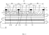
- FIG. 2 is a schematic cross-sectional view, taken along line AA' in FIG. 1
- the color filter substrate 10 may include a base substrate 1, a color conversion layer 2, a covering layer 3, a buffer layer 4, a polarizing layer 5 and a protective layer 6.
- the color conversion layer 2, the covering layer 3, the buffer layer 4, the polarizing layer 5 and the protective layer 6 are sequentially arranged on the base substrate 1 in a direction away from the base substrate 1.
- the color conversion layer 2 is arranged on the base substrate 1
- the covering layer 3 is arranged on a side of the color conversion layer 2 away from the base substrate 1
- the buffer layer 4 is arranged on a side of the covering layer 3 away from the base substrate 1
- the polarizing layer 5 is arranged on a side of the buffer layer 4 away from the base substrate 1
- the protective layer 6 is arrangd on a side of the polarizing layer 5 away from the base substrate 1.
- FIG. 3 is a schematic structural view of a display panel according to examples helpful for understanding but not covered by the claimed invention.
- the display panel 100 may include a color filter substrate 10, an array substrate 20, a backlight module 30, and a liquid crystal layer 40 sandwiched between the color filter substrate 10 and the array substrate 20.
- the base substrate 1 may be a rigid base substrate or a flexible base substrate, including but not limited to a glass base substrate or a polyimide (PI) base substrate.
- PI polyimide
- the color filter substrate 10 may include a plurality of pixels PX, for example, an area surrounded by a dashed frame. It should be understood that the plurality of pixels PX may be arranged in an array, that is, there are multiple rows and multiple columns. In FIG. 1 , only a part of the pixels of the color filter substrate 10 are schematically shown, but not all the pixels. In FIG. 1 , a horizontal direction may be referred to as a row direction, and a vertical direction may be referred to as a column direction. Each pixel PX may include a plurality of sub-pixels SPX for emitting different colors.
- the plurality of sub-pixels SPX may emit different colors such as red, green, blue, yellow, etc., to achieve colorful display.
- the color filter may include at least three sub-pixels SPX, for example, the three sub-pixels SPX may include a first sub-pixel 2R, a second sub-pixel 2G and a third sub-pixel 2B.
- the first sub-pixel 2R is configured to emit light within a first wavelength range
- the second sub-pixel 2G is configured to emit light within a second wavelength range
- the third sub-pixel 2B is configured to emit light within a third wavelength range.
- FIG. 1 in order to clearly show patterns such as a dashed frame and a hatched line, a black matrix is shown with a gray line.
- the first wavelength range, the second wavelength range and the third wavelength range are different from one another.
- the first wavelength range, the second wavelength range and the third wavelength range may correspond to a first color, a second color, and a third color, respectively.
- the first color, the second color and the third color may refer to red, green, and blue, respectively.
- the color filter substrate may also include pixels for emitting other colors, such as pixels for emitting yellow light.
- the color conversion layer 2 may include at least a quantum dot structure.
- the color conversion layer 2 may include a plurality of quantum dot structures for emitting different colors.
- the first sub-pixel 2R may include a first quantum dot structure 221 for emitting light within the first wavelength range
- the second sub-pixel 2G may include a second quantum dot structure 222 for emitting light within the second wavelength range.
- the color conversion layer 2 may also include a quantum dot structure for emitting light within other wavelength ranges, for example, a quantum dot structure for emitting yellow light.
- quantum dot is a semiconductor nanostructure that binds excitons in three spatial directions.
- the quantum dot has the following characteristics: when the quantum dot is excited by light of a predetermined wavelength, the quantum dot may convert the light of the predetermined wavelength into light of another predetermined wavelength, and a wavelength of the light of another predetermined wavelength may be determined by factors such as a constituent material of the quantum dot, a shape of the quantum dot, and a size of the quantum dot.
- the first quantum dot structure 221 may be configured to convert the light within the third wavelength range (for example, blue light) into the light within the first wavelength range (for example, red light), and the second quantum dot structure 222 may be configured to convert the light within the third wavelength range (for example, blue light) into the light within the second wavelength range (for example, green light).
- the third wavelength range for example, blue light
- the second wavelength range for example, green light
- the quantum dot structure may include a plurality of quantum dots
- the first quantum dot structure 221 may include a plurality of first quantum dots 2211, and each of the first quantum dots 2211 may be configured to convert light of the third color into light of the first color.
- the second quantum dot structure 222 may include a plurality of second quantum dots 2221, and each of the second quantum dots 2221 may be configured to convert the light of the third color into light of the second color.
- the material of the quantum dot may be the quantum dot material commonly used in the art, including but not limited to one or more selected from following materials: CdS, CdSe, CdTe, ZnO, ZnS, ZnSe, ZnTe, GaAs, GaP, GaSb, HgS, HgSe, HgTe, InAs, InP, InSb, AlAs, AlP, CuInS, CuInSe and AlSb.
- the material of the quantum dot includes but is not limited to those listed above, and other materials that are the same as or similar to the above substances may also be applied.
- an emission spectrum of the quantum dot may be controlled by changing the size of the quantum dot, that is, the quantum dot is formed into different sizes and may emit light of different colors.
- the size of the quantum dot for emitting red light is mainly about 9-10 nm
- the size of the quantum dot for emitting yellow light is about 8 nm
- the size of the quantum dot for emitting green light is about 7 nm.
- the third sub-pixel 2B may include a transparent structure 223.
- the transparent structure 223 is configured to allow the light that is incident thereon to pass therethrough.
- the transparent structure 223 of the third sub-pixel 2B may be configured to allow the light that is incident thereon and is within the third wavelength range (for example, blue light) to pass therethrough.
- the quantum dot structure may be formed by a photolithography process.
- a thickness of the quantum dot structure may be in a range of 5 ⁇ 15 ⁇ m.
- thicknesses of the first quantum dot structure 221, the second quantum dot structure 222 and the transparent structure 223 may be equal to one another, and all fall within a range of 5 ⁇ 15 ⁇ m.
- the backlight module 30 may include a backlight source that emits the light within the third wavelength range (for example, blue light), such as a blue LED.
- the backlight source of the backlight module 30 may emit blue light with a center wavelength of 450 nm and a full width at half maximum of 30 ⁇ 40 nm.
- the color filter substrate 10 is arranged on a light emitting side of the backlight module 30.
- the first quantum dot structure 221 may emit red light under the excitation of blue light, that is, convert blue light into red light
- the second quantum dot structure 222 may emit green light under the excitation of blue light, that is, convert blue light into green light
- the blue light directly passes through the transparent structure 223.
- the first sub-pixel 2R emits red light
- the second sub-pixel 2G emits green light
- the third sub-pixel 2B emits blue light, so that the display panel may implement colorful display.
- the color conversion layer of the color film substrate includes the quantum dot structure, and advantages of quantum dots may implement the display panel and the display device with a high color gamut and a large viewing angle.
- the first quantum dot structure 221, the second quantum dot structure 222, and/or the transparent structure 223 may also be provided with scattering particles 224 (refer to FIG. 2 ) to improve conversion efficiency for blue light, thereby improving light efficiency of the display panel.
- scattering particles 224 may scatter blue light, which may effectively increase an optical path of blue light in the quantum dot structures and the transparent structure, and increase a probability of blue light incident onto each quantum dot, thereby increasing conversion ratio of blue light into red light and green light. Meanwhile, more blue light may pass through the transparent structure 223. In this way, an overall light efficiency and viewing angle of the display panel may be improved.
- a particle size of the scattering particles 224 may be in a range of 60-500 nm, and a distribution concentration of the scattering particles 224 may be in a range of 1% ⁇ 15%.
- the distribution concentration of the scattering particles 224 may be represented by a volume percentage of the scattering particles in the quantum dot structure or the transparent structure.
- the color filter substrate 10 may further include a filter layer 21, and the filter layer 21 is arranged between the base substrate 1 and a layer where the quantum dot structures and the transparent structure are located.
- the filter layer 21 may include a plurality of filter structures for allow light of different colors to pass through.
- the plurality of filter structures may be arranged in one-to-one correspondence with the plurality of sub-pixels.
- the filter layer 21 may include a first filter structure 211, a second filter structure 212 and a third filter structure 213.
- the first sub-pixel 2R includes the first filter structure 211
- the second sub-pixel 2G includes the second filter structure 212
- the third sub-pixel 2B includes the third filter structure 213.
- the first filter structure 211 is configured to allow the light of the first color to pass through
- the second filter structure 212 is configured to allow the light of the second color to pass through
- the third filter structure 213 is cofigured to allow the light of the third color to pass through.
- the first filter structure 211 is arranged corresponding to the first quantum dot structure 221, that is, the first sub-pixel 2R includes the first filter structure 211 and the first quantum dot structure 221.
- An orthographic projection of the first quantum dot structure 221 on the base substrate 1 falls within an orthographic projection of the first filter structure 211 on the base substrate 1, for example, an area of the orthographic projection of the first quantum dot structure 221 on the base substrate 1 is smaller than an area of the orthographic projection of the first filter structure 211 on the base substrate 1.
- a thickness of the first filter structure 211 may be smaller than a thickness of the first quantum dot structure 221.
- the thickness of the first filter structure 211 may be in a range of 1.5 ⁇ 3.0 ⁇ m
- the thickness of the first quantum dot structure 221 may be in a range of 5-15 ⁇ m.
- the second filter structure 212 is arranged corresponding to the second quantum dot structure 222, that is, the second sub-pixel 2G includes the second filter structure 212 and the second quantum dot structure 222.
- An orthographic projection of the second quantum dot structure 222 on the base substrate 1 falls within an orthographic projection of the second filter structure 212 on the base substrate 1, for example, an area of the orthographic projection of the second quantum dot structure 222 on the base substrate 1 is smaller than an area of the orthographic projection of the second filter structure 212 on the base substrate 1.
- a thickness of the second filter structure 212 may be less than a thickness of the second quantum dot structure 222.
- the thickness of the second filter structure 212 may be in a range of 1.5 ⁇ 3.0 ⁇ m, and the thickness of the second quantum dot structure 222 may be in a range of 5-15 ⁇ m.
- the third filter structure 213 is arranged corresponding to the transparent structure 223, that is, the third sub-pixel 2B includes the third filter structure 213 and the transparent structure 223.
- An orthographic projection of the transparent structure 223 on the base substrate 1 falls within an orthographic projection of the third filter structure 213 on the base substrate 1, for example, an area of the orthographic projection of the transparent structure 223 on the base substrate 1 is smaller than an area of the orthographic projection of the third filter structure 213 on the base substrate 1.
- a thickness of the third filter structure 213 may be less than a thickness of the transparent structure 223.
- the thickness of the third filter structure 213 may be in a range of 1.5 ⁇ 3.0 ⁇ m, and the thickness of the transparent structure 223 may be in a range of 5 ⁇ 15 ⁇ m.
- the filter layer 21 may be arranged between the base substrate 1 and the layer where the quantum dot structures and the transparent structure are located, that is, the filter layer 21 may be arranged on a light emitting side of the quantum dot structures and the transparent structure.
- the first quantum dot structure 221 and the second quantum dot structure 223 may convert blue light into red light and green light, respectively. In addition, there is some blue light that has not been converted by the first quantum dot structure 221 and the second quantum dot structure 223.
- the unconverted blue light may be absorbed, which prevents red light emitted from the first sub-pixel and green light emitted from the second sub-pixel from being mixed with blue light, thereby further improving color gamut of the display panel.
- the filter layer 21 may also absorb external light to avoid poor display caused by external light exciting the quantum dot structure.
- the thicknesses of the first filter structure 211, the second filter structure 212 and the third filter structure 213 are equal to one another, and the thicknesses may be set in a range of 1.5 ⁇ 3.0 ⁇ m. With such an arrangement, the filter layer may meet requirements of sRGB 100% color gamut.
- the thicknesses of the first quantum dot structure 221, the second quantum dot structure 222, and the transparent structure 223 may be equal to one another.
- the thickness of the first filter structure 211 is smaller than the thickness of the first quantum dot structure 221
- the thickness of the second filter structure 212 is smaller than the thickness of the second quantum dot structure 222
- the thickness of the third filter structure 213 is smaller than the thickness of the transparent structure 223.
- the same mask may be configured to manufacture the corresponding filter structure and quantum dot structure. Since the filter structure and the quantum dot structure are made of different materials, and the thickness of the quantum dot structure is relatively large, incomplete curing may occur when the quantum dot structure is manufactured. In this way, part of the material on a side of the quantum dot structure close to the base substrate 1 is easily peeled off. Therefore, the actually manufactured filter structure and quantum dot structure have different cross-sectional shapes.
- the first filter structure 211 may be a trapezoidal structure, Specifically, the first filter structure 211 has a cross-section perpendicular to light-emitting direction (Y direction in figure), a cross-sectional area of the first filter structure 211 gradually decreases in the direction away from the base substrate 1.
- the first quantum dot structure 221 includes a first bottom surface 221A close to the base substrate 1 and a first top surface 221B away from the base substrate 1.
- An orthographic projection of the first bottom surface 221A of the first quantum dot structure 221 on the base substrate 1 falls within an orthographic projection of the first top surface 221B of the first quantum dot structure 221 on the base substrate 1, and an area of the first bottom surface 221A of the first quantum dot structure 221 is smaller than an area of the first top surface 221B of the first quantum dot structure 221.
- an orthographic projection of the first quantum dot structure 221 on the base substrate 1 falls within an orthographic projection of the first filter structure 211 on the base substrate 1, and an area of the orthographic projection of the first quantum dot structure 221 on the base substrate 1 is smaller than an area of the orthographic projection of the first filter structure 211 on the base substrate 1.
- the second quantum dot structure 222 includes a second bottom surface 222A close to the base substrate 1 and a second top surface 222B away from the base substrate 1.
- An orthographic projection of the second bottom surface 222A of the second quantum dot structure 222 on the base substrate 1 falls within an orthographic projection of the second top surface 222B of the second quantum dot structure 222 on the base substrate 1, and an area of the second bottom surface 222A of the second quantum dot structure 222 is smaller than an area of the second top surface 222B of the second quantum dot structure 222.
- an orthographic projection of the second quantum dot structure 222 on the base substrate 1 falls within an orthographic projection of the second filter structure 212 on the base substrate 1, and an area of the orthographic projection of the second quantum dot structure 222 on the base substrate 1 is smaller than an area of the orthographic projection of the second filter structure 212 on the base substrate 1.
- the color filter substrate 10 may further include a black matrix 8. It should be understood that the black matrix 8 is configured to separate pixels and prevent light leakage and cross-color.
- an arrangement of the black matrix 8 may refer to an arrangement of the black matrix in conventional color filter substrate, which will not be repeated here.
- FIG. 4 is a schematic structural view of a color filter substrate according to examples helpful for understanding but not covered by the claimed invention.
- FIG. 4 differs between the examples shown in FIG. 4 and the above examples will be mainly described, and other structures in examples shown in FIG.4 may refer to the above examples helpful for understanding but not covered by the claimed invention.
- a first sub-pixel 2R includes a first filter structure 211 and a first quantum dot structure 221
- a second sub-pixel 2G includes a second filter structure 212 and a second quantum dot structure 222
- a third sub-pixel 2B includes a third filter structure 213'.
- a thickness of the first filter structure 211 may be equal to a thickness of the second filter structure 212, for example, in a range of 1.5 ⁇ 3.0 ⁇ m.
- a thickness of the first quantum dot structure 221 may be equal to a thickness of the second quantum dot structure 222, for example, in a range of 5-15 ⁇ m.
- a thickness of the third filter structure 213' may be equal to a sum of the thickness of the first filter structure 211 and the thickness of the first quantum dot structure 221.
- an integral third filter structure 213' is provided, instead of the filter structure combined with the transparent structure.
- the third filter structure 213' may allow the light of third color (for example, blue light) to pass therethrough.
- the third filter structure 213' may also be doped with scattering particles 224.
- the particle size of the scattering particles 224 may be in a range of 60-500 nm, and the distribution concentration of the scattering particles 224 may be in a range of 1% ⁇ 15%.
- the distribution concentration of the scattering particles 224 may be represented by a volume percentage of the scattering particles in the quantum dot structure or the transparent structure.
- the first filter structure 211 and the first quantum dot structure 221 of the first sub-pixel 2R are respectively arranged at intervals relative to the second filter structure 212 and the second quantum dot structure 222 of the second sub-pixel 2G.
- the second filter structure 212 and the second quantum dot structure 222 of the second sub-pixel 2G are respectively arranged at intervals relative to the third filter structure 213 and the transparent structure 223 of the third sub-pixel 2B. Due to the gap 8G, there is a difference in height between adjacent sub-pixels. For example, the difference in height may be in a range of 5 ⁇ 15 ⁇ m.
- the covering layer 3 may include a first covering sub-layer 31 and a second covering sub-layer 32.
- the first covering sub-layer 31 is arranged on a surface of a layer where the quantum dot structure and the transparent structure are located away from the base substrate 1, and the first covering sub-layer 31 is filled in the gap 8G.
- the second covering sub-layer 32 is arranged on a surface of the first covering sub-layer 31 away from the base substrate 1.
- a material of the first covering sub-layer 31 may be different from a material of the second covering sub-layer 32.
- the first cover sub-layer 31 may be a thermally cured covering layer. That is, the first covering sub-layer 31 may be cured by heating, for example, a curing temperature may be about 150°C.
- main components of material of the thermally cured covering layer may include silicone resin, acrylic resin, isopropanol, hardener, silicon dioxide, and the like.
- a thickness of the first covering sub-layer 31 may be in a range of 3 ⁇ 7 ⁇ m. The inventor found through research that there is a large difference in height between sub-pixels, and the difference in height may be eliminated by providing the first covering sub-layer 31. Referring to FIG.
- a depth of a recess 31R (corresponding to the gap 8G) in the surface is much smaller than the difference in height, that is, the large difference in height at the gap 8G is eliminated to a certain extent.
- the second covering sub-layer 32 may be a light-curing covering layer, for example, an ultraviolet light-curing covering layer.
- main components of material of the light-curing covering layer may include acrylic resin, isopropanol, hardener, silicon dioxide, photoinitiator, and the like.
- a thickness of the second covering sub-layer 32 may be in a range of 2 ⁇ 3 ⁇ m.
- a leveling property of a material of the second covering sub-layer 32 is greater than a leveling property of a material of the first covering sub-layer 31.
- the second cover sub-layer 32 may be formed through a nanoimprint process. The second covering sub-layer 32 may further eliminate the difference in height.
- the second covering sub-layer 32 may be flattened by a nanoimprinting device, and then cured by ultraviolet light, so that the difference in height may meet the requirements of the NIL process (i.e., nanoimprinting process).
- the difference in height may be reduced to several tens of nanometers, that is, the difference in height is less than or equal to 100 nanometers.
- leveling property refers to an ability of covering material to flow evenly without pores on a surface of covered material.
- the leveling property may be expressed by time required for covering material to reach an even surface.
- the large difference in height may be substantially eliminated.
- the difference in height may be reduced to several tens of nanometers, thereby facilitating formation of subsequent film layers.
- the thickness of the first covering sub-layer 31 is greater than or equal to the thickness of the second covering sub-layer 32.
- the thickness of the first covering sub-layer 31 may be 1 ⁇ 4 times the thickness of the second covering sub-layer 32.
- the thickness of the first covering sub-layer 31 may be twice the thickness of the second covering sub-layer 32.
- the polarizing layer 5 is arranged on a side of the quantum dot structures 221 and 222 away from the base substrate 1, that is, the polarizing layer 5 is located on a light incident side of the quantum dot structures 221 and 222. Since the quantum dot structures 221 and 222 have a depolarization function, if an upper polarizer is arranged on a light emitting side of the quantum dot structures 221 and 222, a gray scale maynot be adjusted. By arranging the polarizing layer 5 on the light incident side of the quantum dot structures 221 and 222, the gray scale display of the display panel may be implemented.
- the polarizing layer 5 may be a wire grid polarizer. Compared with a conventional polarizer, the wire grid polarizer 5 may increase a transmittance of a backlight such as blue light, thereby further improving light efficiency.
- the buffer layer 4 and the protective layer 6 are respectively located on upper and lower sides of the wire grid polarizer 5. That is, the buffer layer 4 is provided on a side of the wire grid polarizer 5 close to the base substrate 1, and the protective layer 6 is provided on a side of the wire grid polarizer 5 away from the base substrate 1.
- FIG. 5 is a schematic structural view of a wire grid polarizer.
- the wire grid polarizer 5 may include a plurality of light shielding elements 51 arranged at intervals and gaps 52 which are respectively located between any two adjacent light shielding elements 51.
- the light shielding element 51 may be made of a metal material such as aluminum or silver.
- the wire grid polarizer 5 has a pitch P
- the light shielding element 51 has a width W1 in a direction perpendicular to a light-emitting direction (X direction in the drawings) and a thickness H1 in the light-emitting direction (Y direction in the drawings)
- the gap 52 has a width W2 in the direction perpendicular to the light-emitting direction and a thickness H2 in the light-emitting direction.
- One light shielding element 51 and one gap 52 constitute a unit, and a plurality of units are periodically arranged in the direction perpendicular to the light emitting direction.
- a size of the unit formed by one light shielding element 51 and one gap 52 in the X direction is the pitch P.
- the pitch P is equal to a sum of the width W1 of the light shielding element 51 and the width W2 of the gap 52.
- a ratio of the width W1 of the light shielding element 51 to the pitch P is called as a duty ratio.
- the thickness H1 of the light shielding element 51 is equal to the thickness H2 of the gap 52, and a thickness of the wire grid polarizer 5 in the light emitting direction may be represented by the thickness H1 of the light shielding element 51.
- the light shielding element 51 is relatively long and thin.
- the light shielding elements 5 are arranged in a substantially parallel manner, and the pitch P is smaller than a wavelength of light that is incident on the wire grid polarizer.
- the pitch P, the duty ratio and the thickness of the wire grid polarizer 5 have a greater impact on performance of the wire grid polarizer.
- the performance includes polarization degree and transmittance of the wire grid polarizer, and a wavelength of light applied with the wire grid polarizer.
- Table 1 Influence of the pitch P on polarization degree and transmittance of blue light pitch P/nm polarization degree transmittance 40 99.9999% 43.7720% 50 99.9999% 43.4653% 80 99.9990% 42.0039% 100 99.9943% 40.6417% 120 99.9957% 40.2171% 140 99.9742% 40.2013% 150 99.9772% 39.0102% 200 99.3520% 36.1003% 250 92.0875% 30.5608% 300 88.5012% 27.3971%
- Table 2 Influence of duty ratio on polarization degree and transmittance of blue light duty ratio polarization degree transmittance 0.3 99.9324% 47.2553% 0.4 99.9949% 43.8460% 0.5 99.9943% 40.6417% 0.6 99.9997% 36.9792%
- the pitch P may be set in a range of 100 ⁇ 140nm.
- the pitch P is less than 100nm, although a large polarization degree and a large transmittance may be obtained, processing of the wire grid polarizer is too difficult; when the pitch P is greater than 140 nm, the polarization degree and the transmittance of the wire grid polarizer are small.
- the duty ratio may be about 0.5 to obtain a large polarization and a large transmittance.
- the thickness may be in a range of 150-200 nm to obtain a large polarization degree and a a large transmittance.
- the buffer layer 4 may include a first buffer sub-layer 41 and a second buffer sub-layer 42.
- the first buffer sub-layer 41 is closer to the wire grid polarizer 5 than the second buffer sub-layer 42.
- a metal layer such as aluminum is usually etched by a dry etching process.
- the buffer layer 4 is arranged between the covering layer 3 and the wire grid polarizer 5, so that the buffer layer 4 may prevent the covering layer 3 from being damaged by the dry etching process, that is, the buffer layer 4 may also function as an etching stop layer.
- the first buffer sub-layer 41 may be composed of a low refractive index material, for example, the first buffer sub-layer 41 may be a silicon oxide layer.
- the second buffer sub-layer 42 may be composed of a high refractive index material, for example, the second buffer sub-layer 42 may be a silicon nitride layer. It should be understood that the low refractive index and the high refractive index here are relative concepts, which are intended to mean that the refractive index of the material of the first buffer sub-layer 41 is smaller than the refractive index of the material of the second buffer sub-layer 42.
- the refractive index of the material of the first buffer sub-layer 41 may be in a range of 1.48-1.52, and the refractive index of the material of the second buffer sub-layer 42 may be about 1.8.
- a gradually-changed gradient in refractive index is formed on a light-emitting side of the wire grid polarizer 5, which may further improve light efficiency of the display panel.
- the second buffer sub-layer 42 is composed of silicon nitride, and the silicon nitride may function to stopping etching, so that the buffer layer may function as an etching stop layer.
- the protection layer 6 may include a first protection sub-layer 61 and a second protection sub-layer 62.
- the first protective sub-layer 61 is closer to the wire grid polarizer 5 than the second protective sub-layer 62.
- the protective layer 6 may also play a role of planarization.
- the first protective sub-layer 61 may be composed of a low refractive index material, for example, the first protective sub-layer 61 may be a silicon oxide layer.
- the second protective sub-layer 62 may be composed of a high refractive index material, for example, the second protective sub-layer 62 may be a silicon nitride layer. It should be understood that the low refractive index and the high refractive index here are relative concepts, which are intended to mean that the refractive index of the material of the first protective sub-layer 61 is smaller than the refractive index of the material of the second protective sub-layer 62.
- the refractive index of the material of the first protective sub-layer 61 may be in a range of 1.48-1.52, and the refractive index of the material of the second protective sub-layer 62 may be about 1.8.
- a gradually-changed gradient in refractive index is formed on a light incident side of the wire grid polarizer 5, which may further improve light efficiency of the display panel.
- the buffer layer 4, the wire grid polarizer 5 and the protective layer 6 together constitute a wire grid polarizer assembly.
- the transmittance of the wire grid polarizer assembly to blue light may be improved.
- a central value of the thickness of the first buffer sub-layer 41 may be 290 nm.
- an actual thickness value may fluctuate in a range of 290nm ⁇ 5%, that is, the thickness of the first buffer sub-layer 41 may be in a range of 275.5 ⁇ 304.5nm.
- a central value of the thickness of the second buffer sub-layer 42 may be 100nm.
- an actual thickness value may also fluctuate in a range of 100nm ⁇ 5%, that is, the thickness of the second buffer sub-layer 42 may be in a range of 95 ⁇ 105nm.
- a central value of the thickness of the first protection sub-layer 61 may be 450nm.
- an actual thickness value may fluctuate in a range of 450nm ⁇ 5%, that is, the thickness of the first protective sub-layer 61 may be in a range of 427.5 ⁇ 472.5nm.
- a central value of the thickness of the second protective sub-layer 62 may be 50nm.
- an actual thickness value may fluctuate in a range of 50nm ⁇ 5%, that is, the thickness of the second protective sub-layer 62 may be in a range of 47.5 ⁇ 52.5 nm.
- both the first buffer sub-layer 41 and the first protection sub-layer 61 may be silicon oxide layers, and the refractive index thereof may be in a range of 1.35-1.65, such as 1.44; and both the second buffer sub-layer 42 and the second protection sub-layer 62 may be silicon nitride layers, and the refractive index thereof may be in a range of 1.6-2.0, such as 1.8.
- FIG. 6 is a graph showing the transmittance of the wire grid polarizer assembly to be used in embodiments of the present invention and the comparative examples. By comparing the examples listed in Table 4 and referring to FIG. 6 , it may be obtained: by designing the thickness and the refractive index of each film layer in the wire grid polarizer assembly to the above-mentioned value or value range, the transmittance of the wire grid polarizer assembly to blue light (within a wavelength range of about 435 ⁇ 480nm) may be increased from 61% to 80%, which may further improve light efficiency of the display panel.
- the color filter substrate 10 may further include an alignment layer 7 on a side of the protective layer 6 away from the base substrate 1.
- the alignment layer 7 may be composed of polyimide (PI).
- the second protective sub-layer 62 composed of silicon nitride is provided. Since an adhesive force between silicon nitride and PI is relatively large, an adhesion between the alignment layer 7 and the protective layer 6 may be increased, which is beneficial to coating the alignment layer.
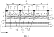
- FIG. 7 is a partial plan view of a color filter substrate according to examples helpful for understanding but not covered by the claimed invention.
- FIG. 8 is a cross-sectional view of the color filter substrate, taken along line BB' in FIG. 7 .
- FIG. 9 is a schematic structural view of a display panel according to examples helpful for understanding but not covered by the claimed invention.
- FIGS. 7-9 differences between the embodiments shown in FIGS. 7-9 and the above examples will be mainly described, and other structures in the examples shown in FIGS. 7-9 may refer to the above examples helpful for understanding but not covered by the claimed invention.
- the isolation bank 9 is schematically made to expose a part of the black matrix 8, but this does not mean that the isolation bank 9 must expose the part of black matrix 8; in addition, the black matrix 8 is shown with a gray color, but this does not mean that the black matrix 8 must be gray.
- the color filter substrate 10 may include a base substrate 1, a color conversion layer 2, a covering layer 3, a buffer layer 4, a polarizing layer 5, a protective layer 6, an alignment layer 7, the isolation bank 9 and a barrier layer 11.
- the color conversion layer 2, the barrier layer 11, the covering layer 3, the buffer layer 4, the polarizing layer 5, the protective layer 6 and the alignment layer 7 are sequentially arranged on the base substrate 1 in a direction away from the base substrate 1.
- the color conversion layer 2 is arranged on the base substrate 1
- the barrier layer 11 is arranged on a side of the color conversion layer 2 away from the base substrate 1
- the covering layer 3 is arranged on a side of the barrier layer 11 away from the base substrate 1
- the buffer layer 4 is arranged on a side of the covering layer 3 away from the base substrate 1
- the polarizing layer 5 is arranged on a side of the buffer layer 4 away from the base substrate 1
- the protective layer 6 is arranged on a side of the polarizing layer 5 away from the base substrate 1
- the alignment layer 7 is arranged on a side of the protective layer 6 away from the base substrate 1.
- a plurality of the isolation banks 9 are arranged on the base substrate 1 to form a plurality of grooves 91 on the base substrate 1.
- the color filter substrate 10 may also include the black matrix 8.
- the black matrix 8 may be configured to separate pixels and prevent light leakage and cross-color.
- the isolation bank 9 may be arranged on a side of the black matrix 8 away from the base substrate 1. An orthographic projection of the isolation bank 9 on the base substrate 1 overlaps with an orthographic projection of the black matrix 8 on the base substrate 1.
- the orthographic projection of the isolation bank 9 on the base substrate 1 may substantially overlap with the orthographic projection of the black matrix 8 on the base substrate 1.
- a material of the isolation bank 9 may be a transparent material.
- the material of the isolation bank 9 may be a black material, the black material has good absorption of light and may effectively reduce color mixing between multiple pixels.
- the material of the isolation bank 9 may be a gray reflective material.
- high refractive index scattering particles such as titanium oxide may be added to the material of the isolation bank 9.
- a size of the scattering particles may be in a range of 60-500 nm, and a distribution concentration of the scattering particles may be in a range of 1% ⁇ 15%.
- the distribution concentration of the scattering particles may be represented by a volume percentage of the scattering particles in the isolation bank. In this way, light reflection may be formed on an interface of the isolation bank 9, so that light efficiency may be improved, and color mixing between a plurality of sub-pixels may be effectively reduced.
- the color filter substrate 10 may include a first sub-pixel 2R, a second sub-pixel 2G, and a third sub-pixel 2B.
- the color filter substrate 10 may further include a filter layer 21, the filter layer 21 is arranged between the base substrate 1 and a layer where the quantum dot structure and the transparent structure are located.
- the filter layer 21 may include a plurality of filter structures for allowing light of different colors to pass therethrough.
- the plurality of filter structures may be arranged in one-to-one correspondence with the plurality of sub-pixels.
- the filter layer 21 may include a first filter structure 211, a second filter structure 212 and a third filter structure 213.
- the isolation bank 9 encloses the plurality of grooves 91 on a side of the filter layer 21 away from the base substrate 1.
- the plurality of grooves 91 may include a first groove 91R, a second groove 91G, and a third groove 91B.
- a first quantum dot structure 221 is located in the first groove 91R
- a second quantum dot structure 222 is located in the second groove 91G
- a transparent structure 223 is located in the third groove 91B.
- the first sub-pixel 2R may include the first quantum dot structure 221 in the first groove 91R
- the second sub-pixel 2G may include the second quantum dot structure 222 in the second groove 91G
- the third sub-pixel 2B may include the transparent structure 223 in the third groove 91B.
- the color conversion layer (in particular, the quantum dot structure) may be formed by a printing process (i.e., an Ink process).
- FIG. 11 is a partial enlarged view of an isolation bank and a black matrix of a color filter substrate according to examples helpful for understanding but not covered by the claimed invention.
- the isolation bank 9 may have a "mushroom" shape.
- the isolation bank 9 may include a neck portion 91A and a body portion 91B.
- a cross section of the body portion 91B in XY plane may be trapezoidal, that is, the body portion 91B has a maximum width Dmax, as shown in FIG. 11 .
- a width of the neck portion 91A is smaller than the maximum width Dmax of the body portion 91B.
- a part of the black matrix 8 between two sub-pixels may have a width Dbm.
- the maximum width Dmax of the body portion 91B is substantially equal to the width Dbm of the black matrix 8.
- an isolation bank 9 may have a columnar shape, for example, the isolation bank 9 extends in Y direction with equal width. And a width of the isolation bank 9 may be equal to a width of a part of a black matrix 8 between two sub-pixels.
- a thickness of the isolation bank 9 may be greater than a sum of thickness of the color conversion layer 2 and thickness of the filter layer 21. In this way, a depth of the formed groove 91 may be greater than the thickness of the color conversion layer 2, thereby facilitating forming the color conversion layer through a printing process.
- the thickness of the filter layer 21 may be in a range of 2.1 ⁇ 3.0 ⁇ m, and the thickness of the color conversion layer 2 may be in a range of 5 ⁇ 10 ⁇ m, so the thickness of the isolation bank 9 may be in a range of 7.1-13 ⁇ m.
- the isolation bank 9 includes a first isolation bank top surface 9T away from the base substrate 1, the first quantum dot structure 221 has a first top surface 221A away from the base substrate 1, the second quantum dot structure 222 has a second top surface 222A away from the base substrate 1, and the first isolation bank top surface 9T is farther away from the base substrate 1 than each of the first top surface 221A and the second top surface 222A.
- the barrier layer 11 is arranged between the color conversion layer 2 and the covering layer 3, specifically, the barrier layer 11 is arranged between the first covering sub-layer 31 and a layer where the quantum dot structures 221, 222 and the transparent structure 223 are located.
- the barrier layer 11 may protect the quantum dot structures (including QD Ink) formed by the printing process from corrosion by water and oxygen, that is, the barrier layer 11 may be configured to resist water and oxygen.
- the barrier layer 11 may be a silicon oxide layer, a thickness of the silicon oxide layer may be in a range of 300-400 nm, and its water and oxygen barrier capacity may be lower than 10 -5 .
- the barrier layer 11 since the barrier layer 11 is made of a low refractive index material such as silicon oxide, it may further improve light efficiency of the display panel.
- a quantum dot layer is formed by a photolithography process, and the quantum dot layer may protect the quantum dots without the barrier layer.
- the barrier layer it is also possible to arrange the barrier layer in the embodiments shown in FIGS. 1 to 4 according to actual needs.
- FIG. 12 is a schematic structural view of a color filter substrate according to examples helpful for understanding but not covered by the claimed invention.
- FIG. 12 differs between the examples shown in FIG. 12 and the above examples will be mainly described, and other structures in the examples shown in FIG.12 may refer to the above examples helpful for understanding but not covered by the claimed invention.
- a first sub-pixel 2R includes a first filter structure 211 and a first quantum dot structure 221
- a second sub-pixel 2G includes a second filter structure 212 and a second quantum dot structure 222
- a third sub-pixel 2B includes a third filter structure 213'.
- a thickness of the first filter structure 211 may be equal to a thickness of the second filter structure 212.
- a thickness of the first quantum dot structure 221 may be equal to a thickness of the second quantum dot structure 222.
- a thickness of the third filter structure 213' may be equal to a sum of the thickness of the first filter structure 211 and the thickness of the first quantum dot structure 221.
- an integral third filter structure 213' is provided, instead of filter structure combined with transparent structure.
- the third filter structure 213' may allow the light of the third color (for example, blue light) to pass therethrough.
- the difference in thickness may be in a range of 5 ⁇ 15 ⁇ m.
- the difference in height causes a surface of the barrier layer 11 away from the base substrate 1 to form an uneven surface.
- the covering layer 3 may include a first cover sub-layer 31 and a second cover sub-layer 32.
- the first covering sub-layer 31 is arranged on a surface of the barrier layer 11 away from the base substrate 1
- the second covering sub-layer 32 is arranged on a surface of the first covering sub-layer 31 away from the base substrate 1.
- the difference in height may be eliminated to form a flattened surface.
- a thickness of the first covering sub-layer 31 is greater than or equal to a thickness of the second covering sub-layer 32.
- the thickness of the first covering sub-layer 31 may be 1 ⁇ 4 times the thickness of the second covering sub-layer 32, for example, the thickness of the first covering sub-layer 31 may be twice the thickness of the second covering sub-layer 32.
- the difference in height may be well eliminated, so that a surface of the covering layer away from the base substrate is flat.
- first covering sub-layer 31 and the second covering sub-layer 32 may refer to the above description, which will not be repeated here.
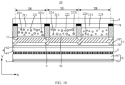
- FIG. 13 is a schematic structural view of a color filter substrate according to embodiments of the present invention.
- FIG. 13 differs between the embodiments shown in FIG. 13 and the above examples helpful for understanding the claimed invention will be mainly described, and other structures in the embodiments shown in FIG. 13 may refer to the above examples helpful for understanding but not covered by the claimed invention.
- the color filter substrate 10 includes a base substrate 1, a filter layer 21, a planarization layer 12, a color conversion layer 2, a covering layer 3, a buffer layer 4, a polarizing layer 5, a protective layer 6, an alignment layer 7, an isolation bank 9 and a barrier layer 11.
- the filter layer 21, the planarization layer 12, the color conversion layer 2, the barrier layer 11, the covering layer 3, the buffer layer 4, the polarizing layer 5, the protective layer 6, and the alignment layer 7 are sequentially arranged on the the base substrate 1 in a direction away from the base substrate 1.
- the filter layer 21 is arranged on the base substrate 1
- the planarization layer 12 is arranged on a side of the filter layer 21 away from the base substrate 1
- the color conversion layer 2 is arranged on a side of the planarization layer 12 away from the base substrate 1
- the barrier layer 11 is arranged on a side of the color conversion layer 2 away from the base substrate 1
- the covering layer 3 is arranged on a side of the barrier layer 11 away from the base substrate 1
- the buffer layer 4 is arranged on a side of the covering layer 3 away from the base substrate 1
- the polarizing layer 5 is arranged on a side of the buffer layer 4 away from the base substrate 1
- the protective layer 6 is arranged on a side of the polarizing layer 5 away from the base substrate 1
- the alignment layer 7 is arranged on a side of the protective layer 6 away from the base substrate 1.
- the filter layer 21 includes a first filter structure 211, a second filter structure 212 and a third filter structure 213.
- a first sub-pixel 2R includes the first filter structure 211
- a second sub-pixel 2G includes the second filter structure 212
- a third sub-pixel 2B includes the third filter structure 213.
- the first filter structure 211 is configured to allow the light of the first color to pass therethrough
- the second filter structure 212 is configured to allow the light of the second color to pass therethrough
- the third filter structure 213 is configured to allow the light of the third color to pass therethrough.
- the color filter substrate 10 also includes a black matrix 8. It should be understood that the black matrix 8 may be configured to separate pixels and prevent light leakage and cross-color.
- the first filter structure 211 of the first sub-pixel 2R and the second filter structure 212 of the second sub-pixel 2G are arranged at intervals
- the second filter structure 212 of the second sub-pixel 2G and the third filter structure 213 of the third sub-pixel 2B are arranged at intervals. Due to the gap, there is a difference in height between adjacent sub-pixels. Since a thickness of the filter layer 21 is small, the difference in height is also small.
- the planarization layer 12 is arranged on the side of the filter layer 21 away from the base substrate 1 to substantially eliminate the difference in height between the sub-pixels.
- a plurality of the isolation banks 9 are arranged on the surface of the planarization layer 12 away from the base substrate 1, so as to form a plurality of grooves 91 on the side of the planarization layer 12 away from the base substrate 1.
- the quantum dot structures are filled in the plurality of grooves 91, respectively.
- the plurality of grooves 91 include a first groove 91R, a second groove 91G, and a third groove 91B.
- the color conversion layer 2 includes a first quantum dot structure 221 and a second quantum dot structure 222.
- the first sub-pixel 2R includes the first quantum dot structure 221 in the first groove 91R
- the second sub-pixel 2G includes the second quantum dot structure 222 in the second groove 91G.
- the third sub-pixel 2B may include a transparent structure 223 in the third groove 91B.
- thicknesses of the first quantum dot structure 221, the second quantum dot structure 222 and the transparent structure 223 may be equal to one another.
- a thickness of the isolation bank 9 may be greater than the thickness of any one of the first quantum dot structure 221, the second quantum dot structure 222 and the transparent structure 223.
- the thickness of any one of the first quantum dot structure 221, the second quantum dot structure 222 and the transparent structure 223 may be in a range of 5 ⁇ 15 ⁇ m.
- the color conversion layer in particular, the quantum dot structure
- the isolation bank by providing the isolation bank, the color conversion layer (in particular, the quantum dot structure) may be formed by a printing process (i.e., an Ink process).
- the display panel 100 may include a color filter substrate 10, an array substrate 20, a backlight module 30, and a liquid crystal layer 40 between the color filter substrate 10 and the array substrate 20.
- the display panel 100 includes the color filter substrate 10 as described above, the display panel 100 should have all structures and advantages of the color filter substrate 10 as described above, which will not be repeated here.
- the array substrate 20 may include: a base substrate 201; and a polarization member 202 on the base substrate 201.
- the polarization member 202 may be located on a surface of the base substrate 201 facing away from the color filter substrate.
- the polarization member 202 is configured to convert light emitted by the backlight module 30 into linearly polarized light.
- the polarization member 202 may be a polarizing film.
- the array substrate 20, the backlight module 30, and the liquid crystal layer 40 may adopt structures of array substrate, backlight module, and liquid crystal layer known in the art, which will not be repeated here.
- the present disclosure also provide a display device, including the display panel as described above.
- the display device 700 may include the display panel as described above.
- the display device may be any product with a display function, such as a smart phone, a wearable smart watch, smart glasses, a tablet computer, a television, a monitor, a notebook computer, a digital photo frame, a navigator, a car monitor, an e-book, etc.
- FIG. 15 is a flowchart of a method for manufacturing a color filter substrate according to the present disclosure. With reference to FIGS. 2 , 4 and 15 in combination, the manufacturing method may include at least following steps.
- step S151 a black matrix 8 is formed on a base substrate 1.
- a filter layer 21 is formed on the base substrate 1.
- the filter layer 21 may include a first filter structure 211, a second filter structure 212, and a third filter structure 213 or 213'.
- the first filter structure 211 is configured to allow light of a first color to pass therethrough, for example, the first filter structure 211 may be a red color film.
- the second filter structure 212 is configured to allow light of a second color to pass therethrough, for example, the second filter structure 212 may be a green color film.
- the third filter structure 213 or 213' is configured to allow light of a third color to pass therethrough, for example, the third filter structure 213 or 213' may be a blue color film.
- the first filter structure 211, the second filter structure 212 and the third filter structure 213 or 213' may be formed by a photolithography process.
- step S 153 a quantum dot structure is formed on a side of the filter layer 21 away from the base substrate 1.
- a first quantum dot structure 221 and a second quantum dot structure 222 may be formed by the photolithography process.
- the first quantum dot structure 221 corresponds to the first filter structure 211, and the first quantum dot structure 221 and the first filter structure 211 may be formed by the same mask.
- the second quantum dot structure 222 corresponds to the second filter structure 212, and the second quantum dot structure 222 and the second filter structure 212 may be formed by the same mask.
- a transparent structure 223 corresponding to the third filter structure 213 may also be formed on a side of the filter layer 21 away from the base substrate 1.
- step S154 a first covering sub-layer 31 is formed on a side of the quantum dot structure away from the base substrate 1.
- a first covering material may be coated by spin coating or knife coating.
- the first covering material includes components such as silicone resin, acrylic resin, isopropanol, hardener, and silicon dioxide. Then, the first covering material is cured by thermal curing to form the first covering sub-layer 31.
- a curing temperature may be about 150°C.
- step S155 a second covering sub-layer 32 is formed on a side of the first covering sub-layer 31 away from the base substrate 1.
- a second covering material may be coated by spin coating.
- the second covering material includes components such as acrylic resin, isopropanol, hardener, silicon dioxide, and photoinitiator. Then, the second covering material is flattened by a nano-imprint process. The second covering material is cured by light curing to form the second covering sub-layer 32. For example, ultraviolet light may be configured to cure the second covering material.
- step S156 a buffer layer 4, a polarizing layer 5 and a protective layer 6 are sequentially formed on a side of the second covering sub-layer 32 away from the base substrate 1.
- FIG. 16 is a flowchart of a method for manufacturing a color filter substrate according to the present disclosure. With reference to FIGS. 8 and 16 in combination, the manufacturing method may include at least following steps.
- step S161 a black matrix 8 is formed on a base substrate 1.
- a filter layer 21 is formed on the base substrate 1.
- the filter layer 21 may include a first filter structure 211, a second filter structure 212, and a third filter structure 213 or 213'.
- an isolation bank 9 is formed on a side of the black matrix 8 away from the base substrate 1.
- the isolation bank 9 is located between two adjacent filter structures to form a plurality of grooves 91 on a side of the filter structure away from the base substrate 1.
- step S164 quantum dot structures are formed in the plurality of grooves 91, respectively.
- a first quantum dot structure 221 and a second quantum dot structure 222 may be formed by an inkjet printing process.
- the first quantum dot structure 221 corresponds to the first filter structure 211
- the second quantum dot structure 222 corresponds to the second filter structure 212.
- a transparent structure 223 corresponding to the third filter structure 213 may also be formed on a side of the filter layer 21 away from the base substrate 1.
- step S165 a barrier layer 11 is formed on a side of the quantum dot structure away from the base substrate 1.
- step S166 a first covering sub-layer 31 is formed on a side of the barrier layer 11 away from the base substrate 1.
- a first covering material may be coated by spin coating or knife coating.
- the first covering material includes components such as silicone resin, acrylic resin, isopropanol, hardener, and silicon dioxide. Then, the first covering material is cured by thermal curing to form the first covering sub-layer 31.
- a curing temperature may be about 150°C.
- step S167 a second covering sub-layer 32 is formed on a side of the first covering sub-layer 31 away from the base substrate 1.
- a second covering material may be coated by spin coating.
- the second covering material includes components such as acrylic resin, isopropanol, hardener, silicon dioxide, and photoinitiator. Then, the second covering material is flattened by a nano-imprint process. The second covering material is cured by light curing to form the second covering sub-layer 32. For example, ultraviolet light may be configured to cure the second covering material.
- step S168 a buffer layer 4, a polarizing layer 5 and a protective layer 6 are sequentially formed on a side of the second covering sub-layer 32 away from the base substrate 1.
Landscapes
- Physics & Mathematics (AREA)
- Nonlinear Science (AREA)
- Mathematical Physics (AREA)
- Chemical & Material Sciences (AREA)
- Crystallography & Structural Chemistry (AREA)
- General Physics & Mathematics (AREA)
- Optics & Photonics (AREA)
- Optical Filters (AREA)
- Liquid Crystal (AREA)
- Devices For Indicating Variable Information By Combining Individual Elements (AREA)
- Polarising Elements (AREA)
Applications Claiming Priority (2)
| Application Number | Priority Date | Filing Date | Title |
|---|---|---|---|
| CN202010057184.0A CN113138484B (zh) | 2020-01-17 | 2020-01-17 | 彩膜基板、显示面板和显示装置 |
| PCT/CN2021/071049 WO2021143641A1 (zh) | 2020-01-17 | 2021-01-11 | 彩膜基板、显示面板和显示装置 |
Publications (3)
| Publication Number | Publication Date |
|---|---|
| EP4092479A1 EP4092479A1 (en) | 2022-11-23 |
| EP4092479A4 EP4092479A4 (en) | 2022-12-07 |
| EP4092479B1 true EP4092479B1 (en) | 2024-07-24 |
Family
ID=76809537
Family Applications (1)
| Application Number | Title | Priority Date | Filing Date |
|---|---|---|---|
| EP21726545.3A Active EP4092479B1 (en) | 2020-01-17 | 2021-01-11 | Color filter substrate, display panel, and display device |
Country Status (5)
| Country | Link |
|---|---|
| US (3) | US11809035B2 (https=) |
| EP (1) | EP4092479B1 (https=) |
| JP (1) | JP7592635B2 (https=) |
| CN (1) | CN113138484B (https=) |
| WO (1) | WO2021143641A1 (https=) |
Families Citing this family (5)
| Publication number | Priority date | Publication date | Assignee | Title |
|---|---|---|---|---|
| KR20210155443A (ko) * | 2020-06-15 | 2021-12-23 | 삼성디스플레이 주식회사 | 디스플레이 장치 |
| KR102883203B1 (ko) * | 2021-04-19 | 2025-11-07 | 삼성디스플레이 주식회사 | 디스플레이 장치의 제조방법 |
| KR20230037099A (ko) * | 2021-09-08 | 2023-03-16 | 삼성디스플레이 주식회사 | 색 변환 기판 및 이를 포함하는 표시 장치 |
| CN114170922A (zh) * | 2021-12-08 | 2022-03-11 | Tcl华星光电技术有限公司 | 显示面板及其制造方法 |
| CN119562699A (zh) * | 2023-09-04 | 2025-03-04 | 京东方科技集团股份有限公司 | 显示面板及其制备方法、显示装置 |
Family Cites Families (26)
| Publication number | Priority date | Publication date | Assignee | Title |
|---|---|---|---|---|
| KR101086476B1 (ko) * | 2004-04-14 | 2011-11-25 | 엘지디스플레이 주식회사 | 액정표시패널 및 그 제조방법 |
| JP5312909B2 (ja) | 2008-11-11 | 2013-10-09 | シャープ株式会社 | カラー有機elディスプレイ用色変換フィルタパネルおよびカラー有機elディスプレイ |
| JP2014199267A (ja) | 2011-08-05 | 2014-10-23 | シャープ株式会社 | 蛍光体基板、表示装置および電子機器 |
| JP2014224835A (ja) | 2011-09-14 | 2014-12-04 | シャープ株式会社 | 表示装置、電子機器および照明装置 |
| CN103278876A (zh) * | 2013-05-28 | 2013-09-04 | 京东方科技集团股份有限公司 | 量子点彩色滤光片及其制作方法、显示装置 |
| JP2016070949A (ja) | 2014-09-26 | 2016-05-09 | 株式会社ジャパンディスプレイ | 表示装置 |
| JP2016142894A (ja) * | 2015-02-02 | 2016-08-08 | 株式会社ジャパンディスプレイ | 表示装置 |
| CN104536198A (zh) * | 2015-02-03 | 2015-04-22 | 京东方科技集团股份有限公司 | 一种显示基板、显示面板和显示装置 |
| US10521053B2 (en) * | 2015-09-16 | 2019-12-31 | 3M Innovative Properties Company | Overcoated patterned conductive layer and methods |
| KR102648400B1 (ko) * | 2016-02-22 | 2024-03-18 | 삼성디스플레이 주식회사 | 양자점 컬러 필터 및 이를 구비하는 표시 장치 |
| KR102661846B1 (ko) * | 2016-06-29 | 2024-04-29 | 삼성디스플레이 주식회사 | 색변환 패널, 이의 제조 방법 및 이를 포함하는 표시 장치 |
| KR102658367B1 (ko) * | 2016-09-28 | 2024-04-18 | 삼성디스플레이 주식회사 | 컬러 필터 및 이를 포함하는 표시 장치 |
| KR101991999B1 (ko) * | 2016-10-31 | 2019-06-21 | 삼성에스디아이 주식회사 | 액정표시장치용 광원측 편광판 및 이를 포함하는 액정표시장치 |
| KR102770511B1 (ko) * | 2016-11-01 | 2025-02-19 | 삼성디스플레이 주식회사 | 색변환 패널, 이의 제조 방법 및 이를 포함하는 표시 장치 |
| KR102661442B1 (ko) * | 2016-11-02 | 2024-04-26 | 삼성디스플레이 주식회사 | 표시 장치 |
| US10139537B2 (en) | 2016-11-22 | 2018-11-27 | Moxtek, Inc. | Multiple-stack wire grid polarizer |
| KR102062587B1 (ko) * | 2017-02-08 | 2020-01-13 | 삼성디스플레이 주식회사 | 표시 장치 |
| KR102601056B1 (ko) * | 2017-02-14 | 2023-11-10 | 삼성디스플레이 주식회사 | 양자점, 색변환 패널 및 이를 포함하는 표시 장치 |
| KR102282060B1 (ko) * | 2017-05-23 | 2021-07-27 | 삼성디스플레이 주식회사 | 표시 장치 및 그 제조 방법 |
| KR102376594B1 (ko) * | 2017-09-04 | 2022-03-21 | 삼성디스플레이 주식회사 | 표시 장치 및 그 제조방법 |
| JP6610702B2 (ja) | 2017-12-25 | 2019-11-27 | セイコーエプソン株式会社 | ワイヤーグリッド偏光素子の製造方法 |
| CN108181678A (zh) * | 2017-12-29 | 2018-06-19 | 深圳市华星光电技术有限公司 | 金属偏光片和包括该金属偏光片的显示装置 |
| KR102548864B1 (ko) * | 2018-01-02 | 2023-06-29 | 삼성디스플레이 주식회사 | 표시 장치 및 이의 구동 방법 |
| CN109300395B (zh) | 2018-10-12 | 2020-11-20 | 京东方科技集团股份有限公司 | 彩膜基板及其制备方法和包含它的量子点显示装置 |
| CN110262114A (zh) * | 2019-06-24 | 2019-09-20 | 京东方科技集团股份有限公司 | 一种彩膜基板、显示面板及显示装置 |
| CN211741778U (zh) | 2020-01-17 | 2020-10-23 | 京东方科技集团股份有限公司 | 彩膜基板、显示面板和显示装置 |
-
2020
- 2020-01-17 CN CN202010057184.0A patent/CN113138484B/zh active Active
-
2021
- 2021-01-11 JP JP2021568953A patent/JP7592635B2/ja active Active
- 2021-01-11 WO PCT/CN2021/071049 patent/WO2021143641A1/zh not_active Ceased
- 2021-01-11 EP EP21726545.3A patent/EP4092479B1/en active Active
- 2021-01-11 US US17/298,267 patent/US11809035B2/en active Active
-
2023
- 2023-09-28 US US18/374,109 patent/US12105372B2/en active Active
-
2024
- 2024-08-22 US US18/812,053 patent/US20240419031A1/en active Pending
Also Published As
| Publication number | Publication date |
|---|---|
| US20220317511A1 (en) | 2022-10-06 |
| US12105372B2 (en) | 2024-10-01 |
| US20240027820A1 (en) | 2024-01-25 |
| US11809035B2 (en) | 2023-11-07 |
| JP7592635B2 (ja) | 2024-12-02 |
| EP4092479A1 (en) | 2022-11-23 |
| US20240419031A1 (en) | 2024-12-19 |
| WO2021143641A1 (zh) | 2021-07-22 |
| CN113138484A (zh) | 2021-07-20 |
| CN113138484B (zh) | 2025-04-29 |
| JP2023510059A (ja) | 2023-03-13 |
| EP4092479A4 (en) | 2022-12-07 |
Similar Documents
| Publication | Publication Date | Title |
|---|---|---|
| EP4092479B1 (en) | Color filter substrate, display panel, and display device | |
| US10367171B2 (en) | Low reflective display device | |
| US11480822B2 (en) | Display substrate comprising a light-reflecting wall having a light-transmissive wall and a light-reflecting layer covering a top surface and side surfaces of the light-transmissive wall, method for manufacturing the same, and display device | |
| US11895893B2 (en) | Display panel including stack of light-converging structure and band-pass filtering structure, manufacturing method thereof, and display apparatus | |
| CN114582246B (zh) | 显示面板及其制造方法和显示装置 | |
| CN114388560B (zh) | 显示面板及其制备方法、显示装置 | |
| US12477919B2 (en) | Display panel, electronic device, and method of manufacturing display panel | |
| US11500239B2 (en) | Display device | |
| KR20220012995A (ko) | 색상 변환 어셈블리, 표시 패널 및 표시 장치 | |
| CN112750862B (zh) | 色彩转换结构、显示装置及色彩转换结构的制备方法 | |
| CN114846615B (zh) | 显示面板及显示装置 | |
| US10746914B2 (en) | Optical member and display device including the same | |
| CN211741778U (zh) | 彩膜基板、显示面板和显示装置 | |
| CN115458566B (zh) | 显示面板、显示装置及显示面板的制作方法 | |
| TWI835778B (zh) | 光學構件及包含其之顯示器 | |
| US11022844B2 (en) | Display device and manufacturing method thereof | |
| US20240099103A1 (en) | Display device and method of manufacturing the same | |
| WO2022236841A1 (zh) | 滤色器结构及其制备方法、显示面板 | |
| CN109445174B (zh) | 一种显示面板及其制备方法、显示装置 |
Legal Events
| Date | Code | Title | Description |
|---|---|---|---|
| STAA | Information on the status of an ep patent application or granted ep patent |
Free format text: STATUS: UNKNOWN |
|
| STAA | Information on the status of an ep patent application or granted ep patent |
Free format text: STATUS: THE INTERNATIONAL PUBLICATION HAS BEEN MADE |
|
| PUAI | Public reference made under article 153(3) epc to a published international application that has entered the european phase |
Free format text: ORIGINAL CODE: 0009012 |
|
| STAA | Information on the status of an ep patent application or granted ep patent |
Free format text: STATUS: REQUEST FOR EXAMINATION WAS MADE |
|
| 17P | Request for examination filed |
Effective date: 20210528 |
|
| AK | Designated contracting states |
Kind code of ref document: A1 Designated state(s): AL AT BE BG CH CY CZ DE DK EE ES FI FR GB GR HR HU IE IS IT LI LT LU LV MC MK MT NL NO PL PT RO RS SE SI SK SM TR |
|
| A4 | Supplementary search report drawn up and despatched |
Effective date: 20221108 |
|
| RIC1 | Information provided on ipc code assigned before grant |
Ipc: G02F 1/13357 20060101ALI20221102BHEP Ipc: G02F 1/1335 20060101AFI20221102BHEP |
|
| DAV | Request for validation of the european patent (deleted) | ||
| DAX | Request for extension of the european patent (deleted) | ||
| GRAP | Despatch of communication of intention to grant a patent |
Free format text: ORIGINAL CODE: EPIDOSNIGR1 |
|
| STAA | Information on the status of an ep patent application or granted ep patent |
Free format text: STATUS: GRANT OF PATENT IS INTENDED |
|
| RIC1 | Information provided on ipc code assigned before grant |
Ipc: G02F 1/13357 20060101ALI20240205BHEP Ipc: G02F 1/1335 20060101AFI20240205BHEP |
|
| INTG | Intention to grant announced |
Effective date: 20240220 |
|
| GRAS | Grant fee paid |
Free format text: ORIGINAL CODE: EPIDOSNIGR3 |
|
| GRAA | (expected) grant |
Free format text: ORIGINAL CODE: 0009210 |
|
| STAA | Information on the status of an ep patent application or granted ep patent |
Free format text: STATUS: THE PATENT HAS BEEN GRANTED |
|
| AK | Designated contracting states |
Kind code of ref document: B1 Designated state(s): AL AT BE BG CH CY CZ DE DK EE ES FI FR GB GR HR HU IE IS IT LI LT LU LV MC MK MT NL NO PL PT RO RS SE SI SK SM TR |
|
| REG | Reference to a national code |
Ref country code: GB Ref legal event code: FG4D |
|
| REG | Reference to a national code |
Ref country code: CH Ref legal event code: EP |
|
| REG | Reference to a national code |
Ref country code: IE Ref legal event code: FG4D Ref country code: DE Ref legal event code: R096 Ref document number: 602021016156 Country of ref document: DE |
|
| REG | Reference to a national code |
Ref country code: LT Ref legal event code: MG9D |
|
| REG | Reference to a national code |
Ref country code: NL Ref legal event code: MP Effective date: 20240724 |
|
| PG25 | Lapsed in a contracting state [announced via postgrant information from national office to epo] |
Ref country code: PT Free format text: LAPSE BECAUSE OF FAILURE TO SUBMIT A TRANSLATION OF THE DESCRIPTION OR TO PAY THE FEE WITHIN THE PRESCRIBED TIME-LIMIT Effective date: 20241125 |
|
| REG | Reference to a national code |
Ref country code: AT Ref legal event code: MK05 Ref document number: 1706847 Country of ref document: AT Kind code of ref document: T Effective date: 20240724 |
|
| PG25 | Lapsed in a contracting state [announced via postgrant information from national office to epo] |
Ref country code: NL Free format text: LAPSE BECAUSE OF FAILURE TO SUBMIT A TRANSLATION OF THE DESCRIPTION OR TO PAY THE FEE WITHIN THE PRESCRIBED TIME-LIMIT Effective date: 20240724 |
|
| PG25 | Lapsed in a contracting state [announced via postgrant information from national office to epo] |
Ref country code: PT Free format text: LAPSE BECAUSE OF FAILURE TO SUBMIT A TRANSLATION OF THE DESCRIPTION OR TO PAY THE FEE WITHIN THE PRESCRIBED TIME-LIMIT Effective date: 20241125 Ref country code: NL Free format text: LAPSE BECAUSE OF FAILURE TO SUBMIT A TRANSLATION OF THE DESCRIPTION OR TO PAY THE FEE WITHIN THE PRESCRIBED TIME-LIMIT Effective date: 20240724 |
|
| PG25 | Lapsed in a contracting state [announced via postgrant information from national office to epo] |
Ref country code: NO Free format text: LAPSE BECAUSE OF FAILURE TO SUBMIT A TRANSLATION OF THE DESCRIPTION OR TO PAY THE FEE WITHIN THE PRESCRIBED TIME-LIMIT Effective date: 20241024 |
|
| PG25 | Lapsed in a contracting state [announced via postgrant information from national office to epo] |
Ref country code: PL Free format text: LAPSE BECAUSE OF FAILURE TO SUBMIT A TRANSLATION OF THE DESCRIPTION OR TO PAY THE FEE WITHIN THE PRESCRIBED TIME-LIMIT Effective date: 20240724 Ref country code: GR Free format text: LAPSE BECAUSE OF FAILURE TO SUBMIT A TRANSLATION OF THE DESCRIPTION OR TO PAY THE FEE WITHIN THE PRESCRIBED TIME-LIMIT Effective date: 20241025 Ref country code: FI Free format text: LAPSE BECAUSE OF FAILURE TO SUBMIT A TRANSLATION OF THE DESCRIPTION OR TO PAY THE FEE WITHIN THE PRESCRIBED TIME-LIMIT Effective date: 20240724 |
|
| PG25 | Lapsed in a contracting state [announced via postgrant information from national office to epo] |
Ref country code: BG Free format text: LAPSE BECAUSE OF FAILURE TO SUBMIT A TRANSLATION OF THE DESCRIPTION OR TO PAY THE FEE WITHIN THE PRESCRIBED TIME-LIMIT Effective date: 20240724 |
|
| PG25 | Lapsed in a contracting state [announced via postgrant information from national office to epo] |
Ref country code: LV Free format text: LAPSE BECAUSE OF FAILURE TO SUBMIT A TRANSLATION OF THE DESCRIPTION OR TO PAY THE FEE WITHIN THE PRESCRIBED TIME-LIMIT Effective date: 20240724 |
|
| PG25 | Lapsed in a contracting state [announced via postgrant information from national office to epo] |
Ref country code: IS Free format text: LAPSE BECAUSE OF FAILURE TO SUBMIT A TRANSLATION OF THE DESCRIPTION OR TO PAY THE FEE WITHIN THE PRESCRIBED TIME-LIMIT Effective date: 20241124 Ref country code: AT Free format text: LAPSE BECAUSE OF FAILURE TO SUBMIT A TRANSLATION OF THE DESCRIPTION OR TO PAY THE FEE WITHIN THE PRESCRIBED TIME-LIMIT Effective date: 20240724 |
|
| PG25 | Lapsed in a contracting state [announced via postgrant information from national office to epo] |
Ref country code: HR Free format text: LAPSE BECAUSE OF FAILURE TO SUBMIT A TRANSLATION OF THE DESCRIPTION OR TO PAY THE FEE WITHIN THE PRESCRIBED TIME-LIMIT Effective date: 20240724 |
|
| PG25 | Lapsed in a contracting state [announced via postgrant information from national office to epo] |
Ref country code: ES Free format text: LAPSE BECAUSE OF FAILURE TO SUBMIT A TRANSLATION OF THE DESCRIPTION OR TO PAY THE FEE WITHIN THE PRESCRIBED TIME-LIMIT Effective date: 20240724 Ref country code: RS Free format text: LAPSE BECAUSE OF FAILURE TO SUBMIT A TRANSLATION OF THE DESCRIPTION OR TO PAY THE FEE WITHIN THE PRESCRIBED TIME-LIMIT Effective date: 20241024 |
|
| PG25 | Lapsed in a contracting state [announced via postgrant information from national office to epo] |
Ref country code: RS Free format text: LAPSE BECAUSE OF FAILURE TO SUBMIT A TRANSLATION OF THE DESCRIPTION OR TO PAY THE FEE WITHIN THE PRESCRIBED TIME-LIMIT Effective date: 20241024 Ref country code: PL Free format text: LAPSE BECAUSE OF FAILURE TO SUBMIT A TRANSLATION OF THE DESCRIPTION OR TO PAY THE FEE WITHIN THE PRESCRIBED TIME-LIMIT Effective date: 20240724 Ref country code: NO Free format text: LAPSE BECAUSE OF FAILURE TO SUBMIT A TRANSLATION OF THE DESCRIPTION OR TO PAY THE FEE WITHIN THE PRESCRIBED TIME-LIMIT Effective date: 20241024 Ref country code: LV Free format text: LAPSE BECAUSE OF FAILURE TO SUBMIT A TRANSLATION OF THE DESCRIPTION OR TO PAY THE FEE WITHIN THE PRESCRIBED TIME-LIMIT Effective date: 20240724 Ref country code: IS Free format text: LAPSE BECAUSE OF FAILURE TO SUBMIT A TRANSLATION OF THE DESCRIPTION OR TO PAY THE FEE WITHIN THE PRESCRIBED TIME-LIMIT Effective date: 20241124 Ref country code: HR Free format text: LAPSE BECAUSE OF FAILURE TO SUBMIT A TRANSLATION OF THE DESCRIPTION OR TO PAY THE FEE WITHIN THE PRESCRIBED TIME-LIMIT Effective date: 20240724 Ref country code: GR Free format text: LAPSE BECAUSE OF FAILURE TO SUBMIT A TRANSLATION OF THE DESCRIPTION OR TO PAY THE FEE WITHIN THE PRESCRIBED TIME-LIMIT Effective date: 20241025 Ref country code: FI Free format text: LAPSE BECAUSE OF FAILURE TO SUBMIT A TRANSLATION OF THE DESCRIPTION OR TO PAY THE FEE WITHIN THE PRESCRIBED TIME-LIMIT Effective date: 20240724 Ref country code: ES Free format text: LAPSE BECAUSE OF FAILURE TO SUBMIT A TRANSLATION OF THE DESCRIPTION OR TO PAY THE FEE WITHIN THE PRESCRIBED TIME-LIMIT Effective date: 20240724 Ref country code: BG Free format text: LAPSE BECAUSE OF FAILURE TO SUBMIT A TRANSLATION OF THE DESCRIPTION OR TO PAY THE FEE WITHIN THE PRESCRIBED TIME-LIMIT Effective date: 20240724 Ref country code: AT Free format text: LAPSE BECAUSE OF FAILURE TO SUBMIT A TRANSLATION OF THE DESCRIPTION OR TO PAY THE FEE WITHIN THE PRESCRIBED TIME-LIMIT Effective date: 20240724 |
|
| PG25 | Lapsed in a contracting state [announced via postgrant information from national office to epo] |
Ref country code: RO Free format text: LAPSE BECAUSE OF FAILURE TO SUBMIT A TRANSLATION OF THE DESCRIPTION OR TO PAY THE FEE WITHIN THE PRESCRIBED TIME-LIMIT Effective date: 20240724 Ref country code: SM Free format text: LAPSE BECAUSE OF FAILURE TO SUBMIT A TRANSLATION OF THE DESCRIPTION OR TO PAY THE FEE WITHIN THE PRESCRIBED TIME-LIMIT Effective date: 20240724 Ref country code: DK Free format text: LAPSE BECAUSE OF FAILURE TO SUBMIT A TRANSLATION OF THE DESCRIPTION OR TO PAY THE FEE WITHIN THE PRESCRIBED TIME-LIMIT Effective date: 20240724 |
|
| PG25 | Lapsed in a contracting state [announced via postgrant information from national office to epo] |
Ref country code: EE Free format text: LAPSE BECAUSE OF FAILURE TO SUBMIT A TRANSLATION OF THE DESCRIPTION OR TO PAY THE FEE WITHIN THE PRESCRIBED TIME-LIMIT Effective date: 20240724 |
|
| PG25 | Lapsed in a contracting state [announced via postgrant information from national office to epo] |
Ref country code: CZ Free format text: LAPSE BECAUSE OF FAILURE TO SUBMIT A TRANSLATION OF THE DESCRIPTION OR TO PAY THE FEE WITHIN THE PRESCRIBED TIME-LIMIT Effective date: 20240724 |
|
| REG | Reference to a national code |
Ref country code: DE Ref legal event code: R097 Ref document number: 602021016156 Country of ref document: DE |
|
| PG25 | Lapsed in a contracting state [announced via postgrant information from national office to epo] |
Ref country code: SK Free format text: LAPSE BECAUSE OF FAILURE TO SUBMIT A TRANSLATION OF THE DESCRIPTION OR TO PAY THE FEE WITHIN THE PRESCRIBED TIME-LIMIT Effective date: 20240724 Ref country code: IT Free format text: LAPSE BECAUSE OF FAILURE TO SUBMIT A TRANSLATION OF THE DESCRIPTION OR TO PAY THE FEE WITHIN THE PRESCRIBED TIME-LIMIT Effective date: 20240724 |
|
| PLBE | No opposition filed within time limit |
Free format text: ORIGINAL CODE: 0009261 |
|
| STAA | Information on the status of an ep patent application or granted ep patent |
Free format text: STATUS: NO OPPOSITION FILED WITHIN TIME LIMIT |
|
| 26N | No opposition filed |
Effective date: 20250425 |
|
| REG | Reference to a national code |
Ref country code: CH Ref legal event code: PL |
|
| PG25 | Lapsed in a contracting state [announced via postgrant information from national office to epo] |
Ref country code: SE Free format text: LAPSE BECAUSE OF FAILURE TO SUBMIT A TRANSLATION OF THE DESCRIPTION OR TO PAY THE FEE WITHIN THE PRESCRIBED TIME-LIMIT Effective date: 20240724 |
|
| PG25 | Lapsed in a contracting state [announced via postgrant information from national office to epo] |
Ref country code: LU Free format text: LAPSE BECAUSE OF NON-PAYMENT OF DUE FEES Effective date: 20250111 Ref country code: MC Free format text: LAPSE BECAUSE OF FAILURE TO SUBMIT A TRANSLATION OF THE DESCRIPTION OR TO PAY THE FEE WITHIN THE PRESCRIBED TIME-LIMIT Effective date: 20240724 |
|
| PG25 | Lapsed in a contracting state [announced via postgrant information from national office to epo] |
Ref country code: BE Free format text: LAPSE BECAUSE OF NON-PAYMENT OF DUE FEES Effective date: 20250131 |
|
| PG25 | Lapsed in a contracting state [announced via postgrant information from national office to epo] |
Ref country code: FR Free format text: LAPSE BECAUSE OF NON-PAYMENT OF DUE FEES Effective date: 20250131 |
|
| PG25 | Lapsed in a contracting state [announced via postgrant information from national office to epo] |
Ref country code: CH Free format text: LAPSE BECAUSE OF NON-PAYMENT OF DUE FEES Effective date: 20250131 |
|
| REG | Reference to a national code |
Ref country code: BE Ref legal event code: MM Effective date: 20250131 |
|
| PG25 | Lapsed in a contracting state [announced via postgrant information from national office to epo] |
Ref country code: IE Free format text: LAPSE BECAUSE OF NON-PAYMENT OF DUE FEES Effective date: 20250111 |
|
| PGFP | Annual fee paid to national office [announced via postgrant information from national office to epo] |
Ref country code: GB Payment date: 20260123 Year of fee payment: 6 |
|
| PGFP | Annual fee paid to national office [announced via postgrant information from national office to epo] |
Ref country code: DE Payment date: 20260121 Year of fee payment: 6 |