EP4089917A1 - Chip packaging module and packaging method thereof, and electronic device with chip packaging module - Google Patents
Chip packaging module and packaging method thereof, and electronic device with chip packaging module Download PDFInfo
- Publication number
- EP4089917A1 EP4089917A1 EP20896027.8A EP20896027A EP4089917A1 EP 4089917 A1 EP4089917 A1 EP 4089917A1 EP 20896027 A EP20896027 A EP 20896027A EP 4089917 A1 EP4089917 A1 EP 4089917A1
- Authority
- EP
- European Patent Office
- Prior art keywords
- chip
- packaging
- substrate
- layer
- module according
- Prior art date
- Legal status (The legal status is an assumption and is not a legal conclusion. Google has not performed a legal analysis and makes no representation as to the accuracy of the status listed.)
- Pending
Links
Images




Classifications
-
- H—ELECTRICITY
- H03—ELECTRONIC CIRCUITRY
- H03H—IMPEDANCE NETWORKS, e.g. RESONANT CIRCUITS; RESONATORS
- H03H3/00—Apparatus or processes specially adapted for the manufacture of impedance networks, resonating circuits, resonators
- H03H3/007—Apparatus or processes specially adapted for the manufacture of impedance networks, resonating circuits, resonators for the manufacture of electromechanical resonators or networks
-
- H—ELECTRICITY
- H03—ELECTRONIC CIRCUITRY
- H03H—IMPEDANCE NETWORKS, e.g. RESONANT CIRCUITS; RESONATORS
- H03H9/00—Networks comprising electromechanical or electro-acoustic elements; Electromechanical resonators
- H03H9/02—Details
- H03H9/05—Holders or supports
- H03H9/10—Mounting in enclosures
- H03H9/1007—Mounting in enclosures for bulk acoustic wave [BAW] devices
- H03H9/1014—Mounting in enclosures for bulk acoustic wave [BAW] devices the enclosure being defined by a frame built on a substrate and a cap, the frame having no mechanical contact with the BAW device
-
- H—ELECTRICITY
- H03—ELECTRONIC CIRCUITRY
- H03H—IMPEDANCE NETWORKS, e.g. RESONANT CIRCUITS; RESONATORS
- H03H3/00—Apparatus or processes specially adapted for the manufacture of impedance networks, resonating circuits, resonators
- H03H3/007—Apparatus or processes specially adapted for the manufacture of impedance networks, resonating circuits, resonators for the manufacture of electromechanical resonators or networks
- H03H3/02—Apparatus or processes specially adapted for the manufacture of impedance networks, resonating circuits, resonators for the manufacture of electromechanical resonators or networks for the manufacture of piezoelectric or electrostrictive resonators or networks
-
- H—ELECTRICITY
- H03—ELECTRONIC CIRCUITRY
- H03H—IMPEDANCE NETWORKS, e.g. RESONANT CIRCUITS; RESONATORS
- H03H9/00—Networks comprising electromechanical or electro-acoustic elements; Electromechanical resonators
- H03H9/02—Details
-
- H—ELECTRICITY
- H03—ELECTRONIC CIRCUITRY
- H03H—IMPEDANCE NETWORKS, e.g. RESONANT CIRCUITS; RESONATORS
- H03H9/00—Networks comprising electromechanical or electro-acoustic elements; Electromechanical resonators
- H03H9/02—Details
- H03H9/05—Holders or supports
- H03H9/0504—Holders or supports for bulk acoustic wave devices
- H03H9/0514—Holders or supports for bulk acoustic wave devices consisting of mounting pads or bumps
- H03H9/0523—Holders or supports for bulk acoustic wave devices consisting of mounting pads or bumps for flip-chip mounting
-
- H—ELECTRICITY
- H10—SEMICONDUCTOR DEVICES; ELECTRIC SOLID-STATE DEVICES NOT OTHERWISE PROVIDED FOR
- H10W—GENERIC PACKAGES, INTERCONNECTIONS, CONNECTORS OR OTHER CONSTRUCTIONAL DETAILS OF DEVICES COVERED BY CLASS H10
- H10W74/00—Encapsulations, e.g. protective coatings
- H10W74/10—Encapsulations, e.g. protective coatings characterised by their shape or disposition
- H10W74/111—Encapsulations, e.g. protective coatings characterised by their shape or disposition the semiconductor body being completely enclosed
- H10W74/129—Encapsulations, e.g. protective coatings characterised by their shape or disposition the semiconductor body being completely enclosed forming a chip-scale package [CSP]
-
- H—ELECTRICITY
- H03—ELECTRONIC CIRCUITRY
- H03H—IMPEDANCE NETWORKS, e.g. RESONANT CIRCUITS; RESONATORS
- H03H3/00—Apparatus or processes specially adapted for the manufacture of impedance networks, resonating circuits, resonators
- H03H3/007—Apparatus or processes specially adapted for the manufacture of impedance networks, resonating circuits, resonators for the manufacture of electromechanical resonators or networks
- H03H2003/0071—Apparatus or processes specially adapted for the manufacture of impedance networks, resonating circuits, resonators for the manufacture of electromechanical resonators or networks of bulk acoustic wave and surface acoustic wave elements in the same process
-
- H—ELECTRICITY
- H10—SEMICONDUCTOR DEVICES; ELECTRIC SOLID-STATE DEVICES NOT OTHERWISE PROVIDED FOR
- H10W—GENERIC PACKAGES, INTERCONNECTIONS, CONNECTORS OR OTHER CONSTRUCTIONAL DETAILS OF DEVICES COVERED BY CLASS H10
- H10W72/00—Interconnections or connectors in packages
- H10W72/851—Dispositions of multiple connectors or interconnections
- H10W72/874—On different surfaces
- H10W72/877—Bump connectors and die-attach connectors
-
- H—ELECTRICITY
- H10—SEMICONDUCTOR DEVICES; ELECTRIC SOLID-STATE DEVICES NOT OTHERWISE PROVIDED FOR
- H10W—GENERIC PACKAGES, INTERCONNECTIONS, CONNECTORS OR OTHER CONSTRUCTIONAL DETAILS OF DEVICES COVERED BY CLASS H10
- H10W90/00—Package configurations
- H10W90/701—Package configurations characterised by the relative positions of pads or connectors relative to package parts
- H10W90/721—Package configurations characterised by the relative positions of pads or connectors relative to package parts of bump connectors
- H10W90/724—Package configurations characterised by the relative positions of pads or connectors relative to package parts of bump connectors between a chip and a stacked insulating package substrate, interposer or RDL
Definitions
- the disclosure relates to the field of semiconductors, and in particular, to a chip packaging structure, a chip packaging method and an electronic device with a chip packaging module.
- FBAR Film Bulk Acoustic Resonator
- BAW bulk acoustic wave resonator
- SAW surface acoustic wave
- Such the FBAR filters are used widely in the field of wireless communication radio frequency, and can be also applicable to the sensing filed such as biology, physics, and medicine due to their high sensitivity.
- the wafer-level packaging is commonly used by far, which not only increases a size of a device, but also has a large number of packaging steps, thereby increasing the packaging cost.
- the wireless communication apparatus gradually develops to be portable, multi-functional, have high performance and low cost, which prompts electronic elements to develop towards miniaturization, high integration, high reliability, and high yield, so do radio frequency filters.
- FIG. 9 is a schematic diagram of a chip packaging structure in the related art.
- FIG. 9 is a schematic diagram of a chip packaging structure in the related art.
- FIG. 9 is a schematic diagram of a chip packaging structure in the related art.
- the peripheral protective layer 17 and the substrate 10 are vacuum pressed such that poor tightness and adhesion are achieved at a contact portion thereof.
- moisture easily penetrates through the oil filter layer 105 to destroy a cavity structure required by the filter chip 15 and affect the performance of the apparatus.
- a chip packaging module which includes a chip, a packaging substrate arranged opposite to the chip, a cavity formed between the packaging substrate and the chip, a first packaging layer, and a second packaging layer.
- the first packaging layer is configured to package the chip on the packaging substrate.
- the second packaging layer is arranged to cover an outer side of the first packaging layer.
- the first packaging layer includes an extension portion extending laterally and outwardly along the packaging substrate, and a lower side of the extension portion covers an upper side of the packaging substrate. An end of the second packaging layer is arranged in surface contact with an upper side of the extension portion.
- An embodiment of the disclosure further provides a chip packaging method.
- the chip packaging method includes: providing a packaging substrate; providing an unpackaged chip; bonding the chip to an upper side of the packaging substrate by flip-chip bonding; providing a first packaging layer in such a manner that the first packaging layer is configured to package the chip on the packaging substrate, the first packaging layer including an extension portion extending laterally and outwardly along the packaging substrate, and a lower side of the extension portion covering the upper side of the packaging substrate; and providing a second packaging layer that covers the first packaging layer, an end of the second packaging layer being arranged in surface contact with an upper side of the extension portion.
- An embodiment of the disclosure also relates to an electronic device including the chip packaging module as described above or a chip packaging module manufactured according to the packaging method as described above.
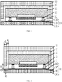
- FIG. 1 is a schematic sectional view of a chip packaging module according to an exemplary embodiment of the present disclosure.
- 10 indicates a substrate, which may be made of ceramic, an organic material or the like.
- the substrate 10 includes three parts, i.e. a bottom substrate 101, a conductive layer 103, and an oil filter layer 105.
- chip bonding structure which may be MBM, a solder ball, a copper pillar and the like.
- an unpackaged filter chip which may be an FBAR chip, SAW chip, or BAW chip.
- 17 indicates a first packaging layer that includes a peripheral protective layer and an adhesive layer between chips.
- 19 indicates a second packaging layer that may also include a peripheral protective layer and an adhesive layer between chips.
- the first packaging layer 17 includes an extension portion extending laterally and outwardly along the packaging substrate.
- the extension portion is a lateral portion in contact with the substrate, and a lower side of the extension portion covers an upper side of the packaging substrate.
- an end of the second packaging layer 19 is arranged in surface contact with an upper side of the extension portion.
- lateral direction is a direction parallel to a surface of the chip or substrate, and more specifically, the lateral direction can correspond to a left-right direction in the drawings.
- the extension portion increases a contact area between the first packaging layer and the substrate, the adhesion between the first packaging layer and the substrate is increased and sealing performance can be improved.
- FIG. 2 is a schematic sectional view of a chip packaging module according to an exemplary embodiment of the present disclosure
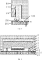
- FIG. 2A is a partially enlarged schematic diagram of a contact portion between a first packaging layer and a substrate in FIG. 2 .
- the substrate has recesses 107 at a position where the extension portion contacts, which facilitates to increase the adhesion of the first packaging layer to the substrate and improves the sealing effect.
- a height of a cavity is HI, which satisfy 10 ⁇ m ⁇ H1 ⁇ 150 ⁇ m.
- a depth of the recess is H2, which satisfy 0.05 ⁇ m ⁇ H2 ⁇ 10 ⁇ m.
- a width W3 of the recess satisfies W3 ⁇ H2.
- the first packaging layer 17 includes an upright portion covering a side surface of the semiconductor chip, and the upright portion is connected to the extension portion.
- An angle ⁇ is formed between a surface of the upright portion facing toward the cavity and the upper side of the substrate, and satisfies 60 ⁇ 90.
- roughness of a side wall that is, roughness of an upright surface AA' in FIG. 2A , is in a range of 10 ⁇ to 10000 ⁇ .
- a first width W1 of the first packaging layer is less than a second width W2 of the second packaging layer, and the first width W1 depends on a thickness of the first packaging layer.
- the first width W1 may satisfy 0 ⁇ W1 ⁇ 50 ⁇ m, and the second width W2 may satisfy W2 ⁇ 15 ⁇ m.
- An upper limit of the second width depends on a difference between a package dimension and a chip dimension.
- a specific value of the width W2 is determined based on the process capability and the difference between the package dimension and the chip dimension.
- FIG. 3 is a schematic sectional view of a chip packaging module according to an exemplary embodiment of the present disclosure.
- a portion of the substrate contacting with the extension portion is formed with bulges.
- FIG. 3A is a partially enlarged schematic diagram of a contact portion between a first packaging layer and a substrate.
- a size of the bulge may be similar to that of the recess shown in FIG. 2 .
- the height of the cavity is HI, which satisfies 10 ⁇ m ⁇ H1 ⁇ 150 ⁇ m
- a height of the bulge is H2, which satisfies 0.05 ⁇ m ⁇ H2 ⁇ 10 ⁇ m.
- a width W3 of the bulge satisfies W3 ⁇ H2.
- the height of the bump may be the same as a thickness of a metal layer on the surface layer of the substrate.
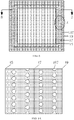
- FIG. 4 is a schematic top view of a packaging structure of a chip packaging module according to an exemplary embodiment of the present disclosure
- FIG. 4A is an enlarged schematic diagram of a part A in FIG. 4
- the substrate is provided with an annular structure to improve the sealing property.
- a recess 107 is a strip recess, and there may be provided with a plurality of strip recesses.
- FIG. 5 is a schematic top view of a packaging structure of a chip packaging module according to an exemplary embodiment of the present disclosure
- FIG. 5A is an enlarged schematic diagram of a part A in FIG. 5
- FIG. 5B is an enlarged schematic diagram of a part A in FIG. 5
- the substrate is provided with an annular structure to improve the sealing property, and the annular structure is formed by an intermittent structure.
- the recess 107 has a rectangular strip shape.
- the rectangular recesses 107 distributed discretely are arranged in a staggered way. In this way, it is beneficial to enhance resistance of a gas passing therethrough in the lateral direction.
- FIG. 6 is a schematic top view of a packaging structure of a chip packaging module according to an exemplary embodiment of the present disclosure
- FIG. 6A is an enlarged schematic diagram of a part A in FIG. 6
- a recess 107 is a circular recess.
- FIGS. 2 to 6A show a sealing reinforcement portion formed by bulges and/or recesses.
- the sealing reinforcement portion is not limited to this.
- the sealing reinforcement portion may include a rough surface structure provided on the upper side of the packaging substrate 10.
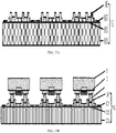
- FIGS. 7A to 7D are flowcharts illustrating a chip packaging method according to an embodiment of the present disclosure.
- the chip packaging method is exemplarily described below with reference to FIGS. 7A to 7D .
- an oil filter layer 105 of a substrate 10 is etched to expose a desired conductive portion 103, bulges 107, and a portion of the substrate 101 to be pressed and contacted.
- a plurality of unpacked filter chips 15 are flip-chip bonded to the substrate 10.
- sealing is performed by vacuum pressing to form a first sealing layer 17 and a second sealing layer 19. Thereafter an air cavity is provided for each of the filter chips 15, and laser cutting is then performed along an upright dotted line.
- a width of the extension portion between two adjacent chips is greater than or equal to 30 ⁇ m, and is twice or more times the first width.
- an expression “twice” is an approximate number, which, for example, may fall in a range of 1.5 times to 2.5 times.
- a packaged chip is obtained after cutting.
- packaging method described above can be used to integrate a plurality of filter chips, or to integrate a plurality of active chips with filter chips.
- FIG. 8 is a schematic sectional view of a chip packaging module according to an exemplary embodiment of the present disclosure, in which two chips are shown.
- the filter chips includes at least one of a bulk acoustic wave filter or a surface acoustic wave filter.
Landscapes
- Physics & Mathematics (AREA)
- Acoustics & Sound (AREA)
- Engineering & Computer Science (AREA)
- Manufacturing & Machinery (AREA)
- Surface Acoustic Wave Elements And Circuit Networks Thereof (AREA)
- Piezo-Electric Or Mechanical Vibrators, Or Delay Or Filter Circuits (AREA)
- Structures Or Materials For Encapsulating Or Coating Semiconductor Devices Or Solid State Devices (AREA)
Abstract
Description
- The disclosure relates to the field of semiconductors, and in particular, to a chip packaging structure, a chip packaging method and an electronic device with a chip packaging module.
- As basic elements of an electronic apparatus, electronic devices have been widely applied, and their applications cover mobile phones, automobiles, home appliances and the like. In addition, technologies such as artificial intelligence, Internet of Things and 5G communication that will change the world in the future still need and rely on the electronic devices.
- As an important member of the piezoelectric devices, a Film Bulk Acoustic Resonator (FBAR, also referred to as a bulk acoustic wave resonator (BAW)) is very important in the field of communication, and especially, an FBAR filter has gained a growing market share in the field of radio frequency filters. The traditional surface acoustic wave (SAW) filters and ceramic filters are gradually replaced by the FBAR filters due to their small size, high resonant frequency, high quality factor, large power capacity, good roll-off effect, and other excellent characteristics. Such the FBAR filters are used widely in the field of wireless communication radio frequency, and can be also applicable to the sensing filed such as biology, physics, and medicine due to their high sensitivity.
- In general, there are specific packaging requirements for the film bulk acoustic resonators in different application environments. The wafer-level packaging is commonly used by far, which not only increases a size of a device, but also has a large number of packaging steps, thereby increasing the packaging cost. In recent years, with rapid development of wireless mobile communication technologies, the wireless communication apparatus gradually develops to be portable, multi-functional, have high performance and low cost, which prompts electronic elements to develop towards miniaturization, high integration, high reliability, and high yield, so do radio frequency filters.
- In recent years, the packaging technology with a simple process and low cost has developed rapidly while satisfying the packaging requirements. However, the airtightness and reliability of the packaging structure still need to be improved.
-
FIG. 9 is a schematic diagram of a chip packaging structure in the related art. InFIG. 9 : - 10 indicates a substrate, which may be made of ceramic, an organic material or the like, and includes three parts, i.e. a
bottom substrate 101, aconductive layer 103, and anoil filter layer 105; - 11 indicates a chip bonding structure, which may be MBM, a solder ball, a copper pillar and the like;
- 13 indicates a pad;
- 15 indicates an unpackaged filter chip, which may be an FBAR chip, SAW chip, or BAW chip;
- 17 indicates an adhesive layer between chips and a peripheral protective layer;
- 19 indicates an adhesive layer between chips and a peripheral protective layer.
- In a structure shown in
FIG. 9 , the peripheralprotective layer 17 and thesubstrate 10 are vacuum pressed such that poor tightness and adhesion are achieved at a contact portion thereof. In addition, moisture easily penetrates through theoil filter layer 105 to destroy a cavity structure required by thefilter chip 15 and affect the performance of the apparatus. - To solve or alleviate at least one aspect of technical problems existing in the related art, the present disclosure is provided.
- According to an aspect of embodiments of the present disclosure, there is provided a chip packaging module, which includes a chip, a packaging substrate arranged opposite to the chip, a cavity formed between the packaging substrate and the chip, a first packaging layer, and a second packaging layer. The first packaging layer is configured to package the chip on the packaging substrate. The second packaging layer is arranged to cover an outer side of the first packaging layer. The first packaging layer includes an extension portion extending laterally and outwardly along the packaging substrate, and a lower side of the extension portion covers an upper side of the packaging substrate. An end of the second packaging layer is arranged in surface contact with an upper side of the extension portion.
- An embodiment of the disclosure further provides a chip packaging method. The chip packaging method includes: providing a packaging substrate; providing an unpackaged chip; bonding the chip to an upper side of the packaging substrate by flip-chip bonding; providing a first packaging layer in such a manner that the first packaging layer is configured to package the chip on the packaging substrate, the first packaging layer including an extension portion extending laterally and outwardly along the packaging substrate, and a lower side of the extension portion covering the upper side of the packaging substrate; and providing a second packaging layer that covers the first packaging layer, an end of the second packaging layer being arranged in surface contact with an upper side of the extension portion.
- An embodiment of the disclosure also relates to an electronic device including the chip packaging module as described above or a chip packaging module manufactured according to the packaging method as described above.
- The following description and drawings can facilitate to understand these and other features and advantages in various embodiments disclosed in the present disclosure. The same reference signs in the drawings always indicate the same components.
-
FIG. 1 is a schematic sectional view of a chip packaging module according to an exemplary embodiment of the present disclosure. -
FIG. 2 is a schematic sectional view of a chip packaging module according to an exemplary embodiment of the present disclosure. -
FIG. 2A is a partially enlarged schematic diagram of a contact portion between a first packaging layer and a substrate inFIG. 2 . -
FIG. 3 is a schematic sectional view of a chip packaging module according to an exemplary embodiment of the present disclosure. -
FIG. 3A is a partially enlarged schematic diagram of a contact portion between a first packaging layer and a substrate inFIG. 3 . -
FIG. 4 is a schematic top view of a packaging structure of a chip packaging module according to an exemplary embodiment of the present disclosure. -
FIG. 4A is an enlarged schematic diagram of a part A inFIG. 4 . -
FIG. 5 is a schematic top view of a packaging structure of a chip packaging module according to an exemplary embodiment of the present disclosure. -
FIG. 5A is an enlarged schematic diagram of a part A inFIG. 5 . -
FIG. 5B is an enlarged schematic diagram of a part A inFIG. 5 . -
FIG. 6 is a schematic top view of a packaging structure of a chip packaging module according to an exemplary embodiment of the present disclosure. -
FIG. 6A is an enlarged schematic diagram of a part A inFIG. 6 . -
FIGS. 7A to 7D are flowcharts illustrating a chip packaging method according to an embodiment of the present disclosure. -
FIG. 8 is a schematic -sectional view of a chip packaging module according to an exemplary embodiment of the present disclosure, in which two chips are shown. - The technical solutions of the present disclosure will be further described below in detail through embodiments and in conjunction with the drawings. The same or similar reference signs indicate the same or similar components throughout the description. The following description of embodiments of the present disclosure with reference to the drawings is intended to explain the general inventive concept of the present disclosure, and should not be construed as limitation to the present disclosure.
-
FIG. 1 is a schematic sectional view of a chip packaging module according to an exemplary embodiment of the present disclosure. InFIG. 1 :
10 indicates a substrate, which may be made of ceramic, an organic material or the like. In an exemplary embodiment, thesubstrate 10 includes three parts, i.e. abottom substrate 101, aconductive layer 103, and anoil filter layer 105. - 11 indicates a chip bonding structure, which may be MBM, a solder ball, a copper pillar and the like.
- 13 indicates a pad.
- 15 indicates an unpackaged filter chip, which may be an FBAR chip, SAW chip, or BAW chip.
- 17 indicates a first packaging layer that includes a peripheral protective layer and an adhesive layer between chips.
- 19 indicates a second packaging layer that may also include a peripheral protective layer and an adhesive layer between chips.
- As shown in
FIG. 1 , thefirst packaging layer 17 includes an extension portion extending laterally and outwardly along the packaging substrate. InFIG. 1 , the extension portion is a lateral portion in contact with the substrate, and a lower side of the extension portion covers an upper side of the packaging substrate. As shown inFIG. 1 , an end of thesecond packaging layer 19 is arranged in surface contact with an upper side of the extension portion. - In the present disclosure, "upper" and "lower" are determined in such a way that the substrate is at top and the chip is at bottom. In the present disclosure, an expression "lateral direction" is a direction parallel to a surface of the chip or substrate, and more specifically, the lateral direction can correspond to a left-right direction in the drawings.
- In a structure of
FIG. 1 , since the extension portion increases a contact area between the first packaging layer and the substrate, the adhesion between the first packaging layer and the substrate is increased and sealing performance can be improved. -
FIG. 2 is a schematic sectional view of a chip packaging module according to an exemplary embodiment of the present disclosure, andFIG. 2A is a partially enlarged schematic diagram of a contact portion between a first packaging layer and a substrate inFIG. 2 . As shown inFIG. 2 , the substrate hasrecesses 107 at a position where the extension portion contacts, which facilitates to increase the adhesion of the first packaging layer to the substrate and improves the sealing effect. - As shown in
FIG. 2 , a height of a cavity is HI, which satisfy 10 µm≤H1≤150 µm. A depth of the recess is H2, which satisfy 0.05 µm≤H2≤10 µm. A width W3 of the recess satisfies W3≥H2. - In a further embodiment, as shown in
FIGS. 2 and2A , thefirst packaging layer 17 includes an upright portion covering a side surface of the semiconductor chip, and the upright portion is connected to the extension portion. An angle θ is formed between a surface of the upright portion facing toward the cavity and the upper side of the substrate, and satisfies 60<θ<90. As shown inFIG. 2A , in an embodiment, roughness of a side wall, that is, roughness of an upright surface AA' inFIG. 2A , is in a range of 10 Å to 10000 Å. - In a further embodiment of the present disclosure, as shown in
FIG. 2 , a first width W1 of the first packaging layer is less than a second width W2 of the second packaging layer, and the first width W1 depends on a thickness of the first packaging layer. The first width W1 may satisfy 0<W1≤50 µm, and the second width W2 may satisfy W2≥15 µm. An upper limit of the second width depends on a difference between a package dimension and a chip dimension. A specific value of the width W2 is determined based on the process capability and the difference between the package dimension and the chip dimension. -
FIG. 3 is a schematic sectional view of a chip packaging module according to an exemplary embodiment of the present disclosure. A portion of the substrate contacting with the extension portion is formed with bulges.FIG. 3A is a partially enlarged schematic diagram of a contact portion between a first packaging layer and a substrate. A size of the bulge may be similar to that of the recess shown inFIG. 2 . For example, the height of the cavity is HI, which satisfies 10 µm≤H1≤150 µm, and a height of the bulge is H2, which satisfies 0.05 µm≤H2≤ 10 µm. A width W3 of the bulge satisfies W3≥H2. In addition, when the bulge is provided, the height of the bump may be the same as a thickness of a metal layer on the surface layer of the substrate. -
FIG. 4 is a schematic top view of a packaging structure of a chip packaging module according to an exemplary embodiment of the present disclosure, andFIG. 4A is an enlarged schematic diagram of a part A inFIG. 4 . As shown inFIG. 4 , the substrate is provided with an annular structure to improve the sealing property. As shown inFIG. 4A , arecess 107 is a strip recess, and there may be provided with a plurality of strip recesses. -
FIG. 5 is a schematic top view of a packaging structure of a chip packaging module according to an exemplary embodiment of the present disclosure,FIG. 5A is an enlarged schematic diagram of a part A inFIG. 5 , andFIG. 5B is an enlarged schematic diagram of a part A inFIG. 5 . As shown inFIG. 5 , the substrate is provided with an annular structure to improve the sealing property, and the annular structure is formed by an intermittent structure. As shown inFIG. 5A , therecess 107 has a rectangular strip shape. InFIG. 5B , therectangular recesses 107 distributed discretely are arranged in a staggered way. In this way, it is beneficial to enhance resistance of a gas passing therethrough in the lateral direction. -
FIG. 6 is a schematic top view of a packaging structure of a chip packaging module according to an exemplary embodiment of the present disclosure, andFIG. 6A is an enlarged schematic diagram of a part A inFIG. 6 . InFIGS. 6 and 6A , arecess 107 is a circular recess. -
FIGS. 2 to 6A show a sealing reinforcement portion formed by bulges and/or recesses. However, the sealing reinforcement portion is not limited to this. For example, the sealing reinforcement portion may include a rough surface structure provided on the upper side of thepackaging substrate 10. -
FIGS. 7A to 7D are flowcharts illustrating a chip packaging method according to an embodiment of the present disclosure. The chip packaging method is exemplarily described below with reference toFIGS. 7A to 7D . - As shown in
FIG. 7A , anoil filter layer 105 of asubstrate 10 is etched to expose a desiredconductive portion 103, bulges 107, and a portion of thesubstrate 101 to be pressed and contacted. - As shown in
FIG. 7B , a plurality of unpackedfilter chips 15 are flip-chip bonded to thesubstrate 10. - As shown in
FIG. 7C , sealing is performed by vacuum pressing to form afirst sealing layer 17 and asecond sealing layer 19. Thereafter an air cavity is provided for each of the filter chips 15, and laser cutting is then performed along an upright dotted line. - It should be noted that, when a plurality of chips are bonded to the substrate by flip-chip bonding, the chips are spaced apart from each other in the lateral direction. A width of the extension portion between two adjacent chips is greater than or equal to 30 µm, and is twice or more times the first width. As can be understood, an expression "twice" is an approximate number, which, for example, may fall in a range of 1.5 times to 2.5 times.
- As shown in
FIG. 7D , a packaged chip is obtained after cutting. - It should be noted that the packaging method described above can be used to integrate a plurality of filter chips, or to integrate a plurality of active chips with filter chips.
-
FIG. 8 is a schematic sectional view of a chip packaging module according to an exemplary embodiment of the present disclosure, in which two chips are shown. In the present disclosure, the filter chips includes at least one of a bulk acoustic wave filter or a surface acoustic wave filter. - In view of the above, the present disclosure provides following technical solutions.
- 1. A chip packaging module includes:
- a chip;
- a packaging substrate arranged opposite to the chip;
- a cavity formed between the packaging substrate and the chip;
- a first packaging layer configured to package the chip on the packaging substrate; and
- a second packaging layer arranged to cover an outer side of the first packaging layer,
- wherein the first packaging layer includes an extension portion extending laterally and outwardly along the packaging substrate, a lower side of the extension portion covers an upper side of the packaging substrate, and an end of the second packaging layer is arranged in surface contact with an upper side of the extension portion.
- 2. The chip packaging module according to 1, wherein
a part of the packaging substrate at least covered by the extension portion is provided with a sealing reinforcement portion. - 3. The chip packaging module according to 2, wherein
the sealing reinforcement portion includes a recess structure or a bulge structure provided on the upper side of the packaging substrate. - 4. The chip packaging module according to 3, wherein
the recess structure or bulge structure includes a strip-shaped annular array structure, a rectangular array structure, or a circular array structure that is formed by recesses or bulges. - 5. The chip packaging module according to 3, wherein
- a height of the cavity is HI, which satisfies 10 µm≤H1≤150 µm;
- a depth of the recess structure or a height of the bulge structure is H2, which satisfies 0.05 µm ≤H2 ≤10 µm; and
- a width W3 of the recess structure or the bulge structure satisfies W3≥H2.
- 6. The chip packaging module according to 2, wherein
the sealing reinforcement portion includes a rough surface structure provided on the upper side of the packaging substrate. - 7. The chip packaging module according to any one of 1 to 6, wherein
the sealing reinforcement portion is disposed in an annular arrangement. - 8. The chip packaging module according to 7, wherein
the sealing reinforcement portion includes an intermittent structure disposed in an annular arrangement. - 9. The chip packaging module according to 1, wherein
in a cross-sectional view extending through the chip and parallel to an upper surface of the chip, a first width W1 of the first packaging layer is less than a second width W2 of the second packaging layer. - 10. The chip packaging module according to 9, wherein
a range of the first width W1 satisfies 0<W1≤50 µm, and the second width W2 satisfies W2≥15 µm. - 11. The chip packaging module according to any one of 1 to 10, wherein
- the first packaging layer includes an upright portion covering a side surface of the semiconductor chip, and the upright portion is connected with the extension portion; and
- an angle θ is formed between a surface of the upright portion facing toward the cavity and the upper side of the substrate, and satisfies 60<θ<90.
- 12. The chip packaging module according to any one of 1 to 10, wherein
the chip includes at least a filter chip, and the filter chip includes at least one of a bulk acoustic wave filter or a surface acoustic wave filter. - 13. The chip packaging module according to 12, wherein
- the chip is a chip assembly including a plurality of chips, which is arranged on a same layer and spaced apart from each other in a lateral direction;
- in the lateral direction, the plurality of chips is separated from each other by the first packaging layer; and
- the extension portion of the first packaging layer is arranged at an outer side of the chip assembly.
- 14. The chip packaging module according to 13, wherein
the chip assembly includes a plurality of filter chips, or the chip assembly includes filter chips and active chips. - 15. A chip packaging method includes:
- providing a packaging substrate;
- providing an unpackaged chip;
- bonding the chip to an upper side of the packaging substrate by flip-chip bonding;
- providing a first packaging layer in such a manner that the first packaging layer packages the chip on the packaging substrate, the first packaging layer including an extension portion extending laterally and outwardly along the packaging substrate, and a lower side of the extension portion covering the upper side of the packaging substrate; and
- providing a second packaging layer that covers the first packaging layer, an end of the second packaging layer being arranged in surface contact with an upper side of the extension portion.
- 16. The method according to 15, wherein
the providing the packaging substrate further includes providing a sealing reinforcement portion at a predetermined position on the packaging substrate, the predetermined position is covered by the extension portion. - 17. The method according to 15 or 16, wherein
- the bonding the chip to the upper side of the packaging substrate by flip-chip bonding includes bonding a plurality of chips to the upper side of the packaging substrate by flip-chip bonding, wherein the plurality of chips is spaced apart from each other in the lateral direction; and
- the first packaging layer has a first width W1, and in the providing the first packaging layer, a width of the extension portion between two adjacent ones of the plurality of chips is not less than 30 µm, and is twice or more times than the first width W1.
- 18. The method according to 17, wherein
the bonding the chip to the upper side of the packaging substrate by flip-chip bonding includes bonding a plurality of filter chips to the upper side of the packaging substrate by flip-chip bonding or bonding filter chips and active chips to the upper side of the packaging substrate by flip-chip bonding. - 19. The method according to 17 or 18 further includes:
performing cutting between predetermined adjacent chips to form a plurality of independent chip packaging modules. - 20. An electronic device includes the chip packaging module according to any one of 1 to 14 or a chip packaging module manufactured by the chip packaging method according to any one of 15 to 19.
- Although the embodiments of the present disclosure have been shown and described, it should be understood for those skilled in the art that modifications may be made to these embodiments without departing from the principle and spirit of the present disclosure, and the scope thereof is defined by the appended claims and their equivalents.
Claims (20)
- A chip packaging module, comprising:a chip;a packaging substrate arranged opposite to the chip;a cavity formed between the packaging substrate and the chip;a first packaging layer configured to package the chip on the packaging substrate; anda second packaging layer arranged to cover an outer side of the first packaging layer,wherein the first packaging layer comprises an extension portion extending laterally and outwardly along the packaging substrate, a lower side of the extension portion covers an upper side of the packaging substrate, and an end of the second packaging layer is arranged in surface contact with an upper side of the extension portion.
- The chip packaging module according to claim 1, wherein a part of the packaging substrate at least covered by the extension portion is provided with a sealing reinforcement portion.
- The chip packaging module according to claim 2, wherein the sealing reinforcement portion comprises a recess structure or a bulge structure provided on the upper side of the packaging substrate.
- The chip packaging module according to claim 3, wherein the recess structure or bulge structure comprises a strip-shaped annular array structure, a rectangular array structure, or a circular array structure that is formed by recesses or bulges.
- The chip packaging module according to claim 3, wherein a height of the cavity is HI, which satisfies 10 µm ≤ H1 ≤ 150 µm;a depth of the recess structure or a height of the bulge structure is H2, which satisfies 0.05 µm ≤ H2 ≤ 10 µm; anda width of the recess structure or the bulge structure is W3, which satisfies W3≥H2.
- The chip packaging module according to claim 2, wherein the sealing reinforcement portion comprises a rough surface structure provided on the upper side of the packaging substrate.
- The chip packaging module according to any one of claims 1 to 6, wherein the sealing reinforcement portion is disposed in an annular arrangement.
- The chip packaging module according to claim 7, wherein the sealing reinforcement portion comprises an intermittent structure disposed in an annular arrangement.
- The chip packaging module according to claim 1, wherein in a cross-sectional view extending through the chip and parallel to an upper surface of the chip, a first width W1 of the first packaging layer is less than a second width W2 of the second packaging layer.
- The chip packaging module according to claim 9, wherein a range of the first width W1 satisfies 0<W1≤50 µm, and the second width W2 satisfies W2≥15 µm.
- The chip packaging module according to any one of claims 1 to 10, wherein the first packaging layer comprises an upright portion covering a side surface of the semiconductor chip, and the upright portion is connected with the extension portion; and
an angle formed between a surface of the upright portion facing toward the cavity and the upper side of the substrate is θ, which satisfies 60<θ<90. - The chip packaging module according to any one of claims 1 to 10, wherein the chip comprises at least a filter chip, and the filter chip comprises at least one of a bulk acoustic wave filter or a surface acoustic wave filter.
- The chip packaging module according to claim 12, wherein the chip is a chip assembly comprising a plurality of chips, which is arranged in a same layer and spaced apart from each other in a lateral direction;in the lateral direction, the plurality of chips is separated from each other by the first packaging layer; andthe extension portion of the first packaging layer is arranged at an outer side of the chip assembly.
- The chip packaging module according to claim 13, wherein the chip assembly comprises a plurality of filter chips, or the chip assembly comprises filter chips and active chips.
- A chip packaging method, comprising:providing a packaging substrate;providing an unpackaged chip;bonding the chip to an upper side of the packaging substrate by flip-chip bonding;providing a first packaging layer in such a manner that the first packaging layer is configured to package the chip on the packaging substrate, the first packaging layer comprising an extension portion extending laterally and outwardly along the packaging substrate, and a lower side of the extension portion covering the upper side of the packaging substrate; andproviding a second packaging layer that covers the first packaging layer, an end of the second packaging layer being arranged in surface contact with an upper side of the extension portion.
- The method according to claim 15, wherein the providing the packaging substrate further comprises providing a sealing reinforcement portion at a predetermined position on the packaging substrate, the predetermined position is covered by the extension portion.
- The method according to claim 15 or 16, wherein the bonding the chip to the upper side of the packaging substrate by flip-chip bonding comprises bonding a plurality of chips to the upper side of the packaging substrate by flip-chip bonding, wherein the plurality of chips is spaced apart from each other in the lateral direction; and
the first packaging layer has a first width W1, and in the providing the first packaging layer, a width of the extension portion between two adjacent ones of the plurality of chips is not less than 30 µm, and is twice or more times than the first width W1. - The method according to claim 17, wherein the bonding the chip to the upper side of the packaging substrate by flip-chip bonding comprises bonding a plurality of filter chips to the upper side of the packaging substrate by flip-chip bonding or bonding filter chips and active chips to the upper side of the packaging substrate by flip-chip bonding.
- The method according to claim 17 or 18, further comprising:
performing cutting between predetermined adjacent chips to form a plurality of independent chip packaging modules. - An electronic device, comprising the chip packaging module according to any one of claims 1 to 14 or a chip packaging module manufactured by the chip packaging method according to any one of claims 15 to 19.
Applications Claiming Priority (2)
| Application Number | Priority Date | Filing Date | Title |
|---|---|---|---|
| CN201911227573.7A CN111245385B (en) | 2019-12-04 | 2019-12-04 | Chip packaging module, packaging method and electronic device having the module |
| PCT/CN2020/088704 WO2021109443A1 (en) | 2019-12-04 | 2020-05-06 | Chip packaging module and packaging method thereof, and electronic device with chip packaging module |
Publications (2)
| Publication Number | Publication Date |
|---|---|
| EP4089917A1 true EP4089917A1 (en) | 2022-11-16 |
| EP4089917A4 EP4089917A4 (en) | 2024-04-24 |
Family
ID=70879284
Family Applications (1)
| Application Number | Title | Priority Date | Filing Date |
|---|---|---|---|
| EP20896027.8A Pending EP4089917A4 (en) | 2019-12-04 | 2020-05-06 | CHIP ENCAPSULATION MODULE AND ENCAPSULATION METHOD THEREFOR, AND ELECTRONIC DEVICE WITH CHIP ENCAPSULATION MODULE |
Country Status (3)
| Country | Link |
|---|---|
| EP (1) | EP4089917A4 (en) |
| CN (1) | CN111245385B (en) |
| WO (1) | WO2021109443A1 (en) |
Families Citing this family (3)
| Publication number | Priority date | Publication date | Assignee | Title |
|---|---|---|---|---|
| CN111934649B (en) * | 2020-09-16 | 2021-02-23 | 苏州日月新半导体有限公司 | Integrated circuit device and method of manufacturing the same |
| CN113411067B (en) * | 2021-07-01 | 2023-05-26 | 苏州汉天下电子有限公司 | Filter and method for manufacturing the same |
| CN115020400A (en) * | 2022-06-16 | 2022-09-06 | 江苏长电科技股份有限公司 | Module structure of cavity chip device and packaging method |
Family Cites Families (13)
| Publication number | Priority date | Publication date | Assignee | Title |
|---|---|---|---|---|
| US6537892B2 (en) * | 2001-02-02 | 2003-03-25 | Delphi Technologies, Inc. | Glass frit wafer bonding process and packages formed thereby |
| US6933537B2 (en) * | 2001-09-28 | 2005-08-23 | Osram Opto Semiconductors Gmbh | Sealing for OLED devices |
| US6919222B2 (en) * | 2002-10-22 | 2005-07-19 | Agilent Technologies, Inc. | Method for sealing a semiconductor device and apparatus embodying the method |
| US6992400B2 (en) * | 2004-01-30 | 2006-01-31 | Nokia Corporation | Encapsulated electronics device with improved heat dissipation |
| JP2008218811A (en) * | 2007-03-06 | 2008-09-18 | Hitachi Metals Ltd | Functional device package |
| JP5177516B2 (en) * | 2008-06-02 | 2013-04-03 | 太陽誘電株式会社 | Electronic components |
| KR20110054710A (en) * | 2009-11-18 | 2011-05-25 | 한국전자통신연구원 | Device package and manufacturing method thereof |
| WO2014187505A1 (en) * | 2013-05-24 | 2014-11-27 | Epcos Ag | Microelectromechanical systems device package and method for producing the microelectromechanical systems device package |
| CN105958963B (en) * | 2016-05-12 | 2019-03-26 | 锐迪科微电子(上海)有限公司 | A kind of encapsulating structure and its manufacturing method |
| CN106301279A (en) * | 2016-10-31 | 2017-01-04 | 中国电子科技集团公司第二十六研究所 | A kind of thin-film bulk acoustic wave filter encapsulating structure and method for packing |
| WO2019005171A1 (en) * | 2017-06-30 | 2019-01-03 | Intel Corporation | Enclosure for an electronic component |
| CN108735890A (en) * | 2018-05-25 | 2018-11-02 | 张琴 | Quasi- air-tightness surface acoustic wave device encapsulating structure and production method |
| CN109192706B (en) * | 2018-09-07 | 2024-04-12 | 苏州晶方半导体科技股份有限公司 | Chip packaging structure and chip packaging method |
-
2019
- 2019-12-04 CN CN201911227573.7A patent/CN111245385B/en active Active
-
2020
- 2020-05-06 EP EP20896027.8A patent/EP4089917A4/en active Pending
- 2020-05-06 WO PCT/CN2020/088704 patent/WO2021109443A1/en not_active Ceased
Also Published As
| Publication number | Publication date |
|---|---|
| CN111245385B (en) | 2025-03-14 |
| CN111245385A (en) | 2020-06-05 |
| WO2021109443A1 (en) | 2021-06-10 |
| EP4089917A4 (en) | 2024-04-24 |
Similar Documents
| Publication | Publication Date | Title |
|---|---|---|
| US7459829B2 (en) | Surface acoustic wave device and method of manufacturing the same, IC card, and mobile electronic apparatus | |
| US20050104204A1 (en) | Wafer-level package and its manufacturing method | |
| CN102800660A (en) | Module and method of manufacturing a module | |
| KR20170108383A (en) | Element package and manufacturing method for the same | |
| CN111245385B (en) | Chip packaging module, packaging method and electronic device having the module | |
| US20160126443A1 (en) | Packaged device including cavity package with elastic layer within molding compound | |
| JP6368091B2 (en) | module | |
| JP2013225749A (en) | Piezoelectric device and module component | |
| CN113659954B (en) | Bulk acoustic wave resonator, packaging method thereof and electronic equipment | |
| JP2022507738A (en) | Integrated structure of crystal resonator and control circuit and its integrated method | |
| JP2022507728A (en) | Integrated structure of crystal resonator and control circuit and its integrated method | |
| KR20170108377A (en) | Element package and manufacturing method for the same | |
| KR101142150B1 (en) | Surface mounting type semiconductor package, fabrication system and method thereof | |
| JP7233984B2 (en) | Package and package manufacturing method | |
| JP2005110017A (en) | High frequency filter module and manufacturing method thereof | |
| JP2022507726A (en) | Integrated structure of crystal resonator and control circuit and its integrated method | |
| JP2022507406A (en) | Integrated structure of crystal resonator and control circuit and its integrated method | |
| JP2022510125A (en) | Integrated structure of crystal resonator and control circuit and its integrated method | |
| CN116260419A (en) | Filter packaging structure and manufacturing method thereof | |
| JP2003264442A (en) | Method of manufacturing surface acoustic wave device and multiple base substrate | |
| JP2000332572A (en) | Piezo device | |
| CN100474768C (en) | Surface acoustic wave device and method of manufacturing the same, IC card, and mobile electronic apparatus | |
| US20060153388A1 (en) | Integrated and monolithic package structure of acoustic wave device | |
| US20250323621A1 (en) | Isolation using micro/nanoscale piezoelectric acoustic resonator structures | |
| US20250323622A1 (en) | Isolation using micro/nanoscale piezoelectric acoustic resonator structures |
Legal Events
| Date | Code | Title | Description |
|---|---|---|---|
| STAA | Information on the status of an ep patent application or granted ep patent |
Free format text: STATUS: THE INTERNATIONAL PUBLICATION HAS BEEN MADE |
|
| PUAI | Public reference made under article 153(3) epc to a published international application that has entered the european phase |
Free format text: ORIGINAL CODE: 0009012 |
|
| STAA | Information on the status of an ep patent application or granted ep patent |
Free format text: STATUS: REQUEST FOR EXAMINATION WAS MADE |
|
| 17P | Request for examination filed |
Effective date: 20220704 |
|
| AK | Designated contracting states |
Kind code of ref document: A1 Designated state(s): AL AT BE BG CH CY CZ DE DK EE ES FI FR GB GR HR HU IE IS IT LI LT LU LV MC MK MT NL NO PL PT RO RS SE SI SK SM TR |
|
| DAV | Request for validation of the european patent (deleted) | ||
| DAX | Request for extension of the european patent (deleted) | ||
| A4 | Supplementary search report drawn up and despatched |
Effective date: 20240325 |
|
| RIC1 | Information provided on ipc code assigned before grant |
Ipc: H03H 9/10 20060101ALI20240319BHEP Ipc: H03H 9/05 20060101ALI20240319BHEP Ipc: H03H 3/02 20060101ALI20240319BHEP Ipc: H03H 9/02 20060101ALI20240319BHEP Ipc: H01L 23/31 20060101ALI20240319BHEP Ipc: H03H 3/007 20060101AFI20240319BHEP |