EP4089896A1 - Output voltage protection controller using voltage signal dynamically adjusted by offset voltage for controlling output voltage protection of voltage regulator and associated method - Google Patents
Output voltage protection controller using voltage signal dynamically adjusted by offset voltage for controlling output voltage protection of voltage regulator and associated method Download PDFInfo
- Publication number
- EP4089896A1 EP4089896A1 EP22169469.8A EP22169469A EP4089896A1 EP 4089896 A1 EP4089896 A1 EP 4089896A1 EP 22169469 A EP22169469 A EP 22169469A EP 4089896 A1 EP4089896 A1 EP 4089896A1
- Authority
- EP
- European Patent Office
- Prior art keywords
- voltage
- signal
- output voltage
- protection
- output
- Prior art date
- Legal status (The legal status is an assumption and is not a legal conclusion. Google has not performed a legal analysis and makes no representation as to the accuracy of the status listed.)
- Pending
Links
- 238000000034 method Methods 0.000 title claims description 12
- 238000001514 detection method Methods 0.000 claims abstract description 104
- 230000001105 regulatory effect Effects 0.000 claims abstract description 32
- 238000010586 diagram Methods 0.000 description 22
- 230000001276 controlling effect Effects 0.000 description 20
- 239000003990 capacitor Substances 0.000 description 2
- 238000013016 damping Methods 0.000 description 2
- 230000000694 effects Effects 0.000 description 2
- 230000004075 alteration Effects 0.000 description 1
- 238000012986 modification Methods 0.000 description 1
- 230000004048 modification Effects 0.000 description 1
Images



Classifications
-
- H—ELECTRICITY
- H02—GENERATION; CONVERSION OR DISTRIBUTION OF ELECTRIC POWER
- H02H—EMERGENCY PROTECTIVE CIRCUIT ARRANGEMENTS
- H02H9/00—Emergency protective circuit arrangements for limiting excess current or voltage without disconnection
- H02H9/04—Emergency protective circuit arrangements for limiting excess current or voltage without disconnection responsive to excess voltage
-
- G—PHYSICS
- G01—MEASURING; TESTING
- G01R—MEASURING ELECTRIC VARIABLES; MEASURING MAGNETIC VARIABLES
- G01R19/00—Arrangements for measuring currents or voltages or for indicating presence or sign thereof
- G01R19/165—Indicating that current or voltage is either above or below a predetermined value or within or outside a predetermined range of values
- G01R19/16566—Circuits and arrangements for comparing voltage or current with one or several thresholds and for indicating the result not covered by subgroups G01R19/16504, G01R19/16528, G01R19/16533
-
- H—ELECTRICITY
- H02—GENERATION; CONVERSION OR DISTRIBUTION OF ELECTRIC POWER
- H02M—APPARATUS FOR CONVERSION BETWEEN AC AND AC, BETWEEN AC AND DC, OR BETWEEN DC AND DC, AND FOR USE WITH MAINS OR SIMILAR POWER SUPPLY SYSTEMS; CONVERSION OF DC OR AC INPUT POWER INTO SURGE OUTPUT POWER; CONTROL OR REGULATION THEREOF
- H02M1/00—Details of apparatus for conversion
- H02M1/32—Means for protecting converters other than automatic disconnection
-
- G—PHYSICS
- G01—MEASURING; TESTING
- G01R—MEASURING ELECTRIC VARIABLES; MEASURING MAGNETIC VARIABLES
- G01R19/00—Arrangements for measuring currents or voltages or for indicating presence or sign thereof
- G01R19/0038—Circuits for comparing several input signals and for indicating the result of this comparison, e.g. equal, different, greater, smaller (comparing pulses or pulse trains according to amplitude)
-
- G—PHYSICS
- G05—CONTROLLING; REGULATING
- G05F—SYSTEMS FOR REGULATING ELECTRIC OR MAGNETIC VARIABLES
- G05F1/00—Automatic systems in which deviations of an electric quantity from one or more predetermined values are detected at the output of the system and fed back to a device within the system to restore the detected quantity to its predetermined value or values, i.e. retroactive systems
- G05F1/10—Regulating voltage or current
-
- H—ELECTRICITY
- H02—GENERATION; CONVERSION OR DISTRIBUTION OF ELECTRIC POWER
- H02M—APPARATUS FOR CONVERSION BETWEEN AC AND AC, BETWEEN AC AND DC, OR BETWEEN DC AND DC, AND FOR USE WITH MAINS OR SIMILAR POWER SUPPLY SYSTEMS; CONVERSION OF DC OR AC INPUT POWER INTO SURGE OUTPUT POWER; CONTROL OR REGULATION THEREOF
- H02M1/00—Details of apparatus for conversion
- H02M1/0003—Details of control, feedback or regulation circuits
- H02M1/0025—Arrangements for modifying reference values, feedback values or error values in the control loop of a converter
-
- H—ELECTRICITY
- H02—GENERATION; CONVERSION OR DISTRIBUTION OF ELECTRIC POWER
- H02M—APPARATUS FOR CONVERSION BETWEEN AC AND AC, BETWEEN AC AND DC, OR BETWEEN DC AND DC, AND FOR USE WITH MAINS OR SIMILAR POWER SUPPLY SYSTEMS; CONVERSION OF DC OR AC INPUT POWER INTO SURGE OUTPUT POWER; CONTROL OR REGULATION THEREOF
- H02M3/00—Conversion of DC power input into DC power output
- H02M3/02—Conversion of DC power input into DC power output without intermediate conversion into AC
- H02M3/04—Conversion of DC power input into DC power output without intermediate conversion into AC by static converters
- H02M3/10—Conversion of DC power input into DC power output without intermediate conversion into AC by static converters using discharge tubes with control electrode or semiconductor devices with control electrode
- H02M3/145—Conversion of DC power input into DC power output without intermediate conversion into AC by static converters using discharge tubes with control electrode or semiconductor devices with control electrode using devices of a triode or transistor type requiring continuous application of a control signal
- H02M3/155—Conversion of DC power input into DC power output without intermediate conversion into AC by static converters using discharge tubes with control electrode or semiconductor devices with control electrode using devices of a triode or transistor type requiring continuous application of a control signal using semiconductor devices only
- H02M3/156—Conversion of DC power input into DC power output without intermediate conversion into AC by static converters using discharge tubes with control electrode or semiconductor devices with control electrode using devices of a triode or transistor type requiring continuous application of a control signal using semiconductor devices only with automatic control of output voltage or current, e.g. switching regulators
Definitions
- the present invention relates to a voltage regulator design, and more particularly, to an output voltage protection controller using a voltage signal dynamically adjusted by an offset voltage for controlling output voltage protection of a voltage regulator and an associated method.
- a voltage regulator In an electronic device, a voltage regulator is used to supply stable power to electronic loads.
- the voltage regulator is typically designed to maintain an output voltage within specified limits even as an electrical load supported by the voltage regulator changes or as the supply power fluctuates.
- the voltage regulator may fail to maintain a stable output voltage. For example, the output voltage of the voltage regulator may exceed a maximum rated voltage of the electrical load due to faults inside the voltage regulator or faults from external causes such as those in the power distribution lines.
- One of the objectives of the claimed invention is to provide an output voltage protection controller using a voltage signal dynamically adjusted by an offset voltage for controlling output voltage protection of a voltage regulator and an associated method.
- an exemplary output voltage protection controller includes a comparator circuit and a voltage adjustment circuit.
- the comparator circuit is arranged to compare a first voltage signal with a second voltage signal to generate a control signal that controls output voltage protection of a voltage regulator, wherein one of the first voltage signal and the second voltage signal is a feedback voltage derived from an output voltage of the voltage regulator, and another of the first voltage signal and the second voltage signal is a voltage detection threshold.
- the voltage adjustment circuit is arranged to inject an offset voltage to the second voltage signal for dynamically adjusting the second voltage signal during a period in which a target regulated voltage level of the output voltage is a constant.
- an exemplary output voltage protection controller includes a comparator circuit and a voltage adjustment circuit.
- the comparator circuit is arranged to compare a first voltage signal with a second voltage signal to generate a control signal that controls output voltage protection of a voltage regulator, wherein one of the first voltage signal and the second voltage signal is a feedback voltage derived from an output voltage of the voltage regulator, and another of the first voltage signal and the second voltage signal is a voltage detection threshold.
- the voltage adjustment circuit is arranged to receive a sensing signal of an inductor current of the voltage regulator, set an offset voltage according to at least the sensing signal, and inject the offset voltage to the second voltage signal.
- an exemplary output voltage protection control method includes: comparing a first voltage signal with a second voltage signal to generate a control signal that controls output voltage protection of a voltage regulator, wherein one of the first voltage signal and the second voltage signal is a feedback voltage derived from an output voltage of the voltage regulator, and another of the first voltage signal and the second voltage signal is a voltage detection threshold; and during a period in which a target regulated voltage level of the output voltage is a constant, injecting an offset voltage to the second voltage signal for dynamically adjusting the second voltage signal.
- an exemplary output voltage protection control method includes: comparing a first voltage signal with a second voltage signal to generate a control signal that controls output voltage protection of a voltage regulator, wherein one of the first voltage signal and the second voltage signal is a feedback voltage derived from an output voltage of the voltage regulator, and another of the first voltage signal and the second voltage signal is a voltage detection threshold; receiving a sensing signal of an inductor current of the voltage regulator; setting an offset voltage according to at least the sensing signal; and injecting the offset voltage to the second voltage signal.
- a voltage detection threshold e.g. overvoltage detection threshold or undervoltage detection threshold
- the output voltage of a voltage regulator may suffer from unwanted overshoot or undershoot as the load of the voltage regulator suffers from load attacks and load releases.
- a typical voltage regulator using a constant voltage detection threshold e.g. a voltage detection threshold with fixed 840mV that is determined by adding a fixed offset to a constant target regulated voltage level of the output voltage
- may generate the output voltage with larger dynamic damping e.g. a range from -59mv to +200mV
- the present invention proposes an output voltage protection controller which employs a dynamic voltage detection threshold (e.g. dynamic overvoltage detection threshold or dynamic undervoltage detection threshold) .
- a dynamic voltage detection threshold e.g. dynamic overvoltage detection threshold or dynamic undervoltage detection threshold
- a proposed voltage regulator using a dynamic voltage detection threshold may generate the output voltage with smaller dynamic damping (e.g. a range from -43mv to +101mV).
- the use of the proposed dynamic voltage detection threshold e.g. dynamic overvoltage detection threshold or dynamic undervoltage detection threshold
- has no impact on the stability of the voltage regulator. Further details of the proposed output voltage protection controller in a voltage regulator will be described as below, with reference to the accompanying drawings.
- FIG. 1 is a diagram illustrating a voltage regulator according to an embodiment of the present invention.
- the voltage regulator 100 may be a switching voltage regulator.
- the voltage regulator 100 may include a pulse-width modulation controller (labeled as "PWM") 102, a power stage circuit (labeled as "PS") 104, an inductor L, and an output capacitor C.
- PWM pulse-width modulation controller
- PS power stage circuit
- the pulse-width modulation controller 102 can regulate the output voltage VOUT delivered to the load 106 by controlling the power stage circuit 104.
- the power stage circuit 104 may include a high-side switch and a low-side switch controlled by outputs of the pulse-width modulation controller 102.
- the pulse-width modulation controller 102 controls the power stage circuit 104 in response to a difference between the output voltage VOUT and the target regulated voltage level VREFTAR. Hence, with the proper feedback control applied to the power stage circuit 104, a voltage level of the output voltage VOUT will approach the target regulated voltage level VREFTAR. Since a person skilled in the art can readily understand details of pulse-width modulation controller 102, power stage circuit 104, inductor L and output capacitor C, further description is omitted here for brevity.
- the voltage regulator 100 further includes an output voltage protection circuit 110.
- the output voltage protection circuit 110 includes an output voltage protection controller 112 and a protection circuit 114, where the output voltage protection controller 112 includes a voltage adjustment circuit 116 and a comparator circuit 118.
- the switching voltage regulator architecture shown in FIG. 1 is for illustrative purposes only, and is not meant to be a limitation of the present invention. In practice, any voltage regulator using output voltage protection circuit 110 (particularly, output voltage protection controller 112 of output voltage protection circuit 110) falls within the scope of the present invention.
- the comparator circuit 118 is arranged to compare two voltage signals FB and VREF to generate a control signal S EN that controls (enables or disables) output voltage protection of the voltage regulator 100.
- the protection circuit 114 is arranged to selectively enable the output voltage protection of the voltage regulator 100 according to the control signal S EN .
- the output voltage protection of the voltage regulator 100 may be overvoltage protection for preventing the output voltage VOUT from being higher than an acceptable level.
- the output voltage protection of the voltage regulator 100 may be undervoltage protection for preventing the output voltage VOUT from being lower than an acceptable level.
- the voltage signal FB is a feedback voltage derived from the output voltage VOUT of the voltage regulator 100.
- the voltage signal FB may be equal to the output voltage VOUT of the voltage regulator 100.
- the voltage signal VREF is a voltage detection threshold.
- the voltage signal VREF may be an overvoltage detection threshold or an undervoltage detection threshold.
- the voltage adjustment circuit 116 is arranged to set an offset voltage V OS and inject the offset voltage V OS to one of the voltage signals FB and VREF during a period in which the target regulated voltage level VREFTAR of the output voltage VOUT is a constant.
- a voltage detection threshold e.g. overvoltage detection threshold or undervoltage detection threshold
- the voltage adjustment circuit 116 is arranged to inject the offset voltage V OS to the voltage signal VREF.
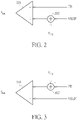
- FIG. 2 is a diagram illustrating one circuit design for achieving the objective of dynamically adjusting the voltage detection threshold according to an embodiment of the present invention.
- the voltage difference viewed from the comparator circuit 118 shown in FIG. 2 is equal to FB - (VREF + Vos) .
- FIG. 3 is a diagram illustrating another circuit design for achieving the objective of dynamically adjusting the voltage detection threshold according to an embodiment of the present invention.
- the voltage difference viewed from the comparator circuit 118 shown in FIG. 3 is equal to (FB -V OS ) - VREF that is the same as the voltage difference FB - (VREF + Vos) viewed from the comparator circuit 118 shown in FIG. 2 .
- the voltage adjustment circuit 116 is responsible for setting the offset voltage V OS used to achieve dynamic adjustment of the voltage signal FB/VREF.
- the adjustment applied to one of the voltage signals FB and VREF may be based on a direct current (DC) level (e.g. constant voltage V DC ), or a time varying signal (e.g., sensing signal IL sen of an inductor current IL of the inductor L), or both of a DC level and a time varying signal, depending upon actual design considerations.
- the adjustment applied to the voltage signal FB/VREF by the offset voltage V OS may increase a voltage level of the voltage signal FB/VREF or decrease a voltage level of the voltage signal FB/VREF, depending upon actual design considerations.
- the voltage adjustment circuit 116 may be implemented by an event-aware voltage adjustment circuit. Hence, the voltage adjustment circuit 116 is further arranged to detect occurrence of an event to generate a detection result, and refer to the detection result to inject the offset voltage V OS to one of the voltage signals FB and VREF. For example, the voltage adjustment circuit 116 may compare the output voltage VOUT (or the voltage signal FB that is indicative of the output voltage VOUT) and an event detection threshold VTH to determine if the event occurs.
- the event detection threshold VTH may be set by the target regulated voltage level VREFTAR minus a specific non-zero level, and the event to be detected is the output voltage VOUT (or the voltage signal FB that is indicative of the output voltage VOUT) being lower than the event detection threshold VTH.
- the event detection threshold VTH may be set by the target regulated voltage level VREFTAR minus a specific non-zero level, and the event to be detected is the output voltage VOUT (or the voltage signal FB that is indicative of the output voltage VOUT) being higher than the event detection threshold VTH. It should be noted that the event to be detected by the voltage adjustment circuit 116 may vary, depending upon actual design considerations.
- FIG. 4 is a diagram illustrating a first example of dynamically adjusting an overvoltage detection threshold used by the output voltage protection controller 112 for controlling overvoltage protection of the voltage regulator 100.
- the voltage signal VREF is used as the overvoltage detection threshold.
- the event detection threshold VTH is set by an existing threshold VREFDIP used by the voltage regulator 100, where the existing threshold VREFDIP is equal to the target regulated voltage VRETAR minus a specific non-zero level DV1.
- An event to be detected by the voltage adjustment circuit 116 is the output voltage VOUT being lower than the event detection threshold VTH.
- the offset voltage V OS is set by the constant voltage V DC , that is, adjustment applied to the overvoltage detection threshold is a DC offset. As shown in FIG.
- the voltage signal VREF has a constant voltage VREFOV during a period in which the event does not occur, and the voltage adjustment circuit 116 injects the offset voltage V OS to the voltage signal VREF during a period in which the event occurs.
- the overvoltage protection threshold is adjusted to a lower level, which can prevent extra energy provided by the inductor from forcing the output voltage VOUT to jump too high.
- the overvoltage protection threshold is recovered from the lower level to a normal level VREFOV for overvoltage protection.
- FIG. 5 is a diagram illustrating a second example of dynamically adjusting an overvoltage detection threshold used by the output voltage protection controller 112 for controlling overvoltage protection of the voltage regulator 100.
- the voltage signal VREF is used as the overvoltage detection threshold.
- the event detection threshold VTH is an additional threshold not belonging to existing thresholds used by the voltage regulator 100.
- the event detection threshold VTH is equal to the target regulated voltage VRETAR minus a specific non-zero level DV2 (DV2 ⁇ DV1) .
- An event to be detected by the voltage adjustment circuit 116 is the output voltage VOUT being lower than the event detection threshold VTH.
- the offset voltage V OS is set by the constant voltage V DC , that is, adjustment applied to the overvoltage detection threshold is a DC offset. As shown in FIG.
- the voltage signal VREF has the constant voltage VREFOV during a period in which the event does not occur, and the voltage adjustment circuit 116 injects the offset voltage V OS to the voltage signal VREF during a period in which the event occurs.
- the overvoltage protection threshold is adjusted to a lower level, which can prevent extra energy provided by the inductor L from forcing the output voltage VOUT to jump too high.
- the overvoltage protection threshold is recovered from the lower level to a normal level VREFOV for overvoltage protection.
- FIG. 6 is a diagram illustrating a third example of dynamically adjusting an overvoltage detection threshold used by the output voltage protection controller 112 for controlling overvoltage protection of the voltage regulator 100.
- the voltage signal VREF is used as the overvoltage detection threshold.
- the event detection threshold VTH is set by an existing threshold VREFDIP used by the voltage regulator 100, where the existing threshold VREFDIP is equal to the target regulated voltage VRETAR minus a specific non-zero level DV1.
- An event to be detected by the voltage adjustment circuit 116 is the output voltage VOUT being lower than the event detection threshold VTH.
- the offset voltage V OS is set according to the sensing signal IL sen of the inductor current IL, that is, adjustment applied to the overvoltage detection threshold is related to the time varying inductor current IL.
- the voltage signal VREF has a constant voltage VREFOV during a period in which the event does not occur
- the voltage adjustment circuit 116 injects the offset voltage V OS (which is a time varying voltage) to the voltage signal VREF during a period in which the event occurs.
- the offset voltage V OS may be set by A* (IL sen -IL avg ), where A is a non-zero ratio, and IL avg is an average value of the inductor current IL.
- the offset voltage V OS may be set by V1-A* (IL sen -IL avg ), where V1 is a DC level, A is a non-zero ratio, and IL avg is an average value of the inductor current IL.
- FIG. 7 is a diagram illustrating a fourth example of dynamically adjusting an overvoltage detection threshold used by the output voltage protection controller 112 for controlling overvoltage protection of the voltage regulator 100.
- the voltage signal VREF is used as the overvoltage detection threshold.
- the event detection threshold VTH is an additional threshold not belonging to existing thresholds used by the voltage regulator 100.
- the event detection threshold VTH is equal to the target regulated voltage VRETAR minus a specific non-zero level DV2 (DV2 ⁇ DV1).
- An event to be detected by the voltage adjustment circuit 116 is the output voltage VOUT being lower than the event detection threshold VTH.
- the offset voltage V OS is set according to the sensing signal IL sen of the inductor current IL, that is, adjustment applied to the overvoltage detection threshold is related to the time varying inductor current IL.
- the voltage signal VREF has a constant voltage VREFOV during a period in which the event does not occur
- the voltage adjustment circuit 116 injects the offset voltage V OS (which is a time varying voltage) to the voltage signal VREF during a period in which the event occurs.
- the offset voltage V OS may be set by A*(IL sen -IL avg ), where A is a non-zero ratio, and IL avg is an average value of the inductor current IL.
- the offset voltage V OS may be set by V1-A* (IL sen -IL avg ), where V1 is a DC level, A is a non-zero ratio, and IL avg is an average value of the inductor current IL.
- FIG. 8 is a diagram illustrating a first example of dynamically adjusting an undervoltage detection threshold used by the output voltage protection controller 112 for controlling undervoltage protection of the voltage regulator 100.
- the voltage signal VREF is used as the undervoltage detection threshold.
- the event detection threshold VTH is set by an existing threshold VREFDIP used by the voltage regulator 100, where the existing threshold VREFDIP is equal to the target regulated voltage VRETAR minus a specific non-zero level DV1.
- An event to be detected by the voltage adjustment circuit 116 is the output voltage VOUT being higher than the event detection threshold VTH.
- the offset voltage V OS is set by the constant voltage V DC , that is, adjustment applied to the overvoltage detection threshold is a DC offset.
- the voltage signal VREF has a constant voltage VREFUV during a period in which the event does not occur, and the voltage adjustment circuit 116 injects the offset voltage V OS to the voltage signal VREF during a period in which the event occurs.
- FIG. 9 is a diagram illustrating a second example of dynamically adjusting an undervoltage detection threshold used by the output voltage protection controller 112 for controlling undervoltage protection of the voltage regulator 100.
- the voltage signal VREF is used as the undervoltage detection threshold.
- the event detection threshold VTH is an additional threshold not belonging to existing thresholds used by the voltage regulator 100.
- the event detection threshold VTH is equal to the target regulated voltage VRETAR minus a specific non-zero level DV3 (DV3 ⁇ DV1) .
- An event to be detected by the voltage adjustment circuit 116 is the output voltage VOUT being higher than the event detection threshold VTH.
- the offset voltage V OS is set by the constant voltage V DC , that is, adjustment applied to the overvoltage detection threshold is a DC offset.
- the voltage signal VREF has the constant voltage VREFUV during a period in which the event does not occur, and the voltage adjustment circuit 116 injects the offset voltage V OS to the voltage signal VREF during a period in which the event occurs.
- FIG. 10 is a diagram illustrating a third example of dynamically adjusting an undervoltage detection threshold used by the output voltage protection controller 112 for controlling undervoltage protection of the voltage regulator 100.
- the voltage signal VREF is used as the undervoltage detection threshold.
- the event detection threshold VTH is set by an existing threshold VREFDIP used by the voltage regulator 100, where the existing threshold VREFDIP is equal to the target regulated voltage VRETAR minus a specific non-zero level DV1.
- An event to be detected by the voltage adjustment circuit 116 is the output voltage VOUT being higher than the event detection threshold VTH.
- the offset voltage V OS is set according to the sensing signal IL sen of the inductor current IL, that is, adjustment applied to the overvoltage detection threshold is related to the time varying inductor current IL.
- the voltage signal VREF has a constant voltage VREFUV during a period in which the event does not occur
- the voltage adjustment circuit 116 injects the offset voltage V OS (which is a time varying voltage) to the voltage signal VREF during a period in which the event occurs.
- the offset voltage V OS may be set by A*(IL sen -IL avg ), where A is a non-zero ratio, and IL avg is an average value of the inductor current IL.
- the offset voltage V OS may be set by V1-A*(IL sen -IL avg ), where V1 is a DC level, A is a non-zero ratio, and IL avg is an average value of the inductor current IL.
- FIG. 11 is a diagram illustrating a fourth example of dynamically adjusting an undervoltage detection threshold used by the output voltage protection controller 112 for controlling undervoltage protection of the voltage regulator 100.
- the voltage signal VREF is used as the undervoltage detection threshold.
- the event detection threshold VTH is an additional threshold not belonging to existing thresholds used by the voltage regulator 100.
- the event detection threshold VTH is equal to the target regulated voltage VRETAR minus a specific non-zero level DV3 ( DV3 ⁇ DV1 ).
- An event to be detected by the voltage adjustment circuit 116 is the output voltage VOUT being higher than the event detection threshold VTH.
- the offset voltage V OS is set according to the sensing signal IL sen of the inductor current IL, that is, adjustment applied to the overvoltage detection threshold is related to the time varying inductor current IL.
- the voltage signal VREF has a constant voltage VREFUV during a period in which the event does not occur
- the voltage adjustment circuit 116 injects the offset voltage V OS (which is a time varying voltage) to the voltage signal VREF during a period in which the event occurs.
- the offset voltage V OS may be set by A*(IL Sen -IL avg ), where A is a non-zero ratio, and IL avg is an average value of the inductor current IL.
- the offset voltage V OS may be set by V1-A*(IL sen -IL avg ), where V1 is a DC level, A is a non-zero ratio, and IL avg is an average value of the inductor current IL.
- the offset voltages V OS shown in FIGs. 4-11 are for illustrative purposes only, and are not meant to be limitations of the present invention.
- the offset voltage V OS may be set by an upward DC shift.
- the offset voltage V OS may be set by a downward DC shift.
- the offset voltage V OS may be a time varying voltage with a ramp-up waveform related to the inductor current.
- the offset voltage V OS may be a time varying voltage with a ramp-down waveform related to the inductor current.
- the present invention may also be defined by the following numbered clauses.
Landscapes
- Engineering & Computer Science (AREA)
- Power Engineering (AREA)
- Physics & Mathematics (AREA)
- General Physics & Mathematics (AREA)
- Electromagnetism (AREA)
- Radar, Positioning & Navigation (AREA)
- Automation & Control Theory (AREA)
- Dc-Dc Converters (AREA)
- Emergency Protection Circuit Devices (AREA)
- Control Of Eletrric Generators (AREA)
- Protection Of Static Devices (AREA)
- Continuous-Control Power Sources That Use Transistors (AREA)
Abstract
Description
- This application claims the benefit of
U.S. Provisional Application No. 63/186,194, filed on May 10th, 2021 U.S. Provisional Application No. 63/222,488, filed on July 16th, 2021 - The present invention relates to a voltage regulator design, and more particularly, to an output voltage protection controller using a voltage signal dynamically adjusted by an offset voltage for controlling output voltage protection of a voltage regulator and an associated method.
- In an electronic device, a voltage regulator is used to supply stable power to electronic loads. The voltage regulator is typically designed to maintain an output voltage within specified limits even as an electrical load supported by the voltage regulator changes or as the supply power fluctuates. However, due to certain factors, the voltage regulator may fail to maintain a stable output voltage. For example, the output voltage of the voltage regulator may exceed a maximum rated voltage of the electrical load due to faults inside the voltage regulator or faults from external causes such as those in the power distribution lines. Thus, there is a need for an innovative output voltage protection design of a voltage regulator.
- One of the objectives of the claimed invention is to provide an output voltage protection controller using a voltage signal dynamically adjusted by an offset voltage for controlling output voltage protection of a voltage regulator and an associated method.
- According to a first aspect of the present invention, an exemplary output voltage protection controller is disclosed. The exemplary output voltage protection controller includes a comparator circuit and a voltage adjustment circuit. The comparator circuit is arranged to compare a first voltage signal with a second voltage signal to generate a control signal that controls output voltage protection of a voltage regulator, wherein one of the first voltage signal and the second voltage signal is a feedback voltage derived from an output voltage of the voltage regulator, and another of the first voltage signal and the second voltage signal is a voltage detection threshold. The voltage adjustment circuit is arranged to inject an offset voltage to the second voltage signal for dynamically adjusting the second voltage signal during a period in which a target regulated voltage level of the output voltage is a constant.
- According to a second aspect of the present invention, an exemplary output voltage protection controller is disclosed. The exemplary output voltage protection controller includes a comparator circuit and a voltage adjustment circuit. The comparator circuit is arranged to compare a first voltage signal with a second voltage signal to generate a control signal that controls output voltage protection of a voltage regulator, wherein one of the first voltage signal and the second voltage signal is a feedback voltage derived from an output voltage of the voltage regulator, and another of the first voltage signal and the second voltage signal is a voltage detection threshold. The voltage adjustment circuit is arranged to receive a sensing signal of an inductor current of the voltage regulator, set an offset voltage according to at least the sensing signal, and inject the offset voltage to the second voltage signal.
- According to a third aspect of the present invention, an exemplary output voltage protection control method is disclosed. The exemplary output voltage protection control method includes: comparing a first voltage signal with a second voltage signal to generate a control signal that controls output voltage protection of a voltage regulator, wherein one of the first voltage signal and the second voltage signal is a feedback voltage derived from an output voltage of the voltage regulator, and another of the first voltage signal and the second voltage signal is a voltage detection threshold; and during a period in which a target regulated voltage level of the output voltage is a constant, injecting an offset voltage to the second voltage signal for dynamically adjusting the second voltage signal.
- According to a fourth aspect of the present invention, an exemplary output voltage protection control method is disclosed. The exemplary output voltage protection control method includes: comparing a first voltage signal with a second voltage signal to generate a control signal that controls output voltage protection of a voltage regulator, wherein one of the first voltage signal and the second voltage signal is a feedback voltage derived from an output voltage of the voltage regulator, and another of the first voltage signal and the second voltage signal is a voltage detection threshold; receiving a sensing signal of an inductor current of the voltage regulator; setting an offset voltage according to at least the sensing signal; and injecting the offset voltage to the second voltage signal.
- These and other objectives of the present invention will no doubt become obvious to those of ordinary skill in the art after reading the following detailed description of the preferred embodiment that is illustrated in the various figures and drawings.
-
-
FIG. 1 is a diagram illustrating a voltage regulator according to an embodiment of the present invention. -
FIG. 2 is a diagram illustrating one circuit design for achieving the objective of dynamically adjusting the voltage detection threshold according to an embodiment of the present invention. -
FIG. 3 is a diagram illustrating another circuit design for achieving the objective of dynamically adjusting the voltage detection threshold according to an embodiment of the present invention. -
FIG. 4 is a diagram illustrating a first example of dynamically adjusting an overvoltage detection threshold used by the output voltage protection controller for controlling overvoltage protection of the voltage regulator. -
FIG. 5 is a diagram illustrating a second example of dynamically adjusting an overvoltage detection threshold used by the output voltage protection controller for controlling overvoltage protection of the voltage regulator. -
FIG. 6 is a diagram illustrating a third example of dynamically adjusting an overvoltage detection threshold used by the output voltage protection controller for controlling overvoltage protection of the voltage regulator. -
FIG. 7 is a diagram illustrating a fourth example of dynamically adjusting an overvoltage detection threshold used by the output voltage protection controller for controlling overvoltage protection of the voltage regulator. -
FIG. 8 is a diagram illustrating a first example of dynamically adjusting an undervoltage detection threshold used by the output voltage protection controller for controlling undervoltage protection of the voltage regulator. -
FIG. 9 is a diagram illustrating a second example of dynamically adjusting an undervoltage detection threshold used by the output voltage protection controller for controlling undervoltage protection of the voltage regulator. -
FIG. 10 is a diagram illustrating a third example of dynamically adjusting an undervoltage detection threshold used by the outputvoltage protection controller 112 for controlling undervoltage protection of the voltage regulator. -
FIG. 11 is a diagram illustrating a fourth example of dynamically adjusting an undervoltage detection threshold used by the output voltage protection controller for controlling undervoltage protection of the voltage regulator. - Certain terms are used throughout the following description and claims, which refer to particular components. As one skilled in the art will appreciate, electronic equipment manufacturers may refer to a component by different names. This document does not intend to distinguish between components that differ in name but not in function. In the following description and in the claims, the terms "include" and "comprise" are used in an open-ended fashion, and thus should be interpreted to mean "include, but not limited to ...". Also, the term "couple" is intended to mean either an indirect or direct electrical connection. Accordingly, if one device is coupled to another device, that connection may be through a direct electrical connection, or through an indirect electrical connection via other devices and connections.
- If a voltage detection threshold (e.g. overvoltage detection threshold or undervoltage detection threshold) is set by a constant level under a constant target regulated voltage level of an output voltage, the output voltage of a voltage regulator may suffer from unwanted overshoot or undershoot as the load of the voltage regulator suffers from load attacks and load releases. For example, a typical voltage regulator using a constant voltage detection threshold (e.g. a voltage detection threshold with fixed 840mV that is determined by adding a fixed offset to a constant target regulated voltage level of the output voltage) may generate the output voltage with larger dynamic damping (e.g. a range from -59mv to +200mV) . To address this issue, the present invention proposes an output voltage protection controller which employs a dynamic voltage detection threshold (e.g. dynamic overvoltage detection threshold or dynamic undervoltage detection threshold) . For example, a proposed voltage regulator using a dynamic voltage detection threshold (e.g. a voltage detection threshold with a dynamic range from 768mV to 840mV) may generate the output voltage with smaller dynamic damping (e.g. a range from -43mv to +101mV). In addition, the use of the proposed dynamic voltage detection threshold (e.g. dynamic overvoltage detection threshold or dynamic undervoltage detection threshold) has no impact on the stability of the voltage regulator. Further details of the proposed output voltage protection controller in a voltage regulator will be described as below, with reference to the accompanying drawings.
-
FIG. 1 is a diagram illustrating a voltage regulator according to an embodiment of the present invention. Thevoltage regulator 100 may be a switching voltage regulator. As shown inFIG. 1 , thevoltage regulator 100 may include a pulse-width modulation controller (labeled as "PWM") 102, a power stage circuit (labeled as "PS") 104, an inductor L, and an output capacitor C. The pulse-width modulation controller 102 can regulate the output voltage VOUT delivered to theload 106 by controlling thepower stage circuit 104. For example, thepower stage circuit 104 may include a high-side switch and a low-side switch controlled by outputs of the pulse-width modulation controller 102. When a target regulated voltage level VREFTAR is set, the pulse-width modulation controller 102 controls thepower stage circuit 104 in response to a difference between the output voltage VOUT and the target regulated voltage level VREFTAR. Hence, with the proper feedback control applied to thepower stage circuit 104, a voltage level of the output voltage VOUT will approach the target regulated voltage level VREFTAR. Since a person skilled in the art can readily understand details of pulse-width modulation controller 102,power stage circuit 104, inductor L and output capacitor C, further description is omitted here for brevity. - The
voltage regulator 100 further includes an outputvoltage protection circuit 110. In this embodiment, the outputvoltage protection circuit 110 includes an outputvoltage protection controller 112 and aprotection circuit 114, where the outputvoltage protection controller 112 includes avoltage adjustment circuit 116 and acomparator circuit 118. It should be noted that the switching voltage regulator architecture shown inFIG. 1 is for illustrative purposes only, and is not meant to be a limitation of the present invention. In practice, any voltage regulator using output voltage protection circuit 110 (particularly, outputvoltage protection controller 112 of output voltage protection circuit 110) falls within the scope of the present invention. - The
comparator circuit 118 is arranged to compare two voltage signals FB and VREF to generate a control signal SEN that controls (enables or disables) output voltage protection of thevoltage regulator 100. Specifically, theprotection circuit 114 is arranged to selectively enable the output voltage protection of thevoltage regulator 100 according to the control signal SEN. In some embodiments of the present invention, the output voltage protection of thevoltage regulator 100 may be overvoltage protection for preventing the output voltage VOUT from being higher than an acceptable level. In some other embodiments of the present invention, the output voltage protection of thevoltage regulator 100 may be undervoltage protection for preventing the output voltage VOUT from being lower than an acceptable level. The voltage signal FB is a feedback voltage derived from the output voltage VOUT of thevoltage regulator 100. For example, the voltage signal FB may be equal to the output voltage VOUT of thevoltage regulator 100. The voltage signal VREF is a voltage detection threshold. For example, the voltage signal VREF may be an overvoltage detection threshold or an undervoltage detection threshold. - The
voltage adjustment circuit 116 is arranged to set an offset voltage VOS and inject the offset voltage VOS to one of the voltage signals FB and VREF during a period in which the target regulated voltage level VREFTAR of the output voltage VOUT is a constant. In other words, under a condition where a constant target regulated voltage level VREFTAR is set for the output voltage VOUT, an effect of dynamically adjusting a voltage detection threshold (e.g. overvoltage detection threshold or undervoltage detection threshold) can be achieved through injecting the offset voltage VOS to one of the voltage signals FB and VREF. - In one exemplary design, the
voltage adjustment circuit 116 is arranged to inject the offset voltage VOS to the voltage signal VREF.FIG. 2 is a diagram illustrating one circuit design for achieving the objective of dynamically adjusting the voltage detection threshold according to an embodiment of the present invention. Thevoltage adjustment circuit 116 may include anadder 202 that is configured to add the offset voltage VOS to the voltage signal VREF (i.e. VREF = VREF + VOS). The voltage difference viewed from thecomparator circuit 118 shown inFIG. 2 is equal to FB - (VREF + Vos) . - Since the
comparator circuit 118 determines the control signal SEN by comparing the voltage signal FB with the voltage signal VREF, an effect of dynamically adjusting the voltage signal VREF is the same as that of dynamically adjusting the voltage signal FB. In another exemplary design, thevoltage adjustment circuit 116 is arranged to inject the offset voltage VOS to the voltage signal FB.FIG. 3 is a diagram illustrating another circuit design for achieving the objective of dynamically adjusting the voltage detection threshold according to an embodiment of the present invention. Thevoltage adjustment circuit 116 may include asubtractor 302 that is configured to subtract the offset voltage VOS from the voltage signal FB (i.e. FB = FB - VOS). The voltage difference viewed from thecomparator circuit 118 shown inFIG. 3 is equal to (FB -VOS) - VREF that is the same as the voltage difference FB - (VREF + Vos) viewed from thecomparator circuit 118 shown inFIG. 2 . - As mentioned above, the
voltage adjustment circuit 116 is responsible for setting the offset voltage VOS used to achieve dynamic adjustment of the voltage signal FB/VREF. The adjustment applied to one of the voltage signals FB and VREF may be based on a direct current (DC) level (e.g. constant voltage VDC), or a time varying signal (e.g., sensing signal ILsen of an inductor current IL of the inductor L), or both of a DC level and a time varying signal, depending upon actual design considerations. Furthermore, the adjustment applied to the voltage signal FB/VREF by the offset voltage VOS may increase a voltage level of the voltage signal FB/VREF or decrease a voltage level of the voltage signal FB/VREF, depending upon actual design considerations. - In this embodiment, the
voltage adjustment circuit 116 may be implemented by an event-aware voltage adjustment circuit. Hence, thevoltage adjustment circuit 116 is further arranged to detect occurrence of an event to generate a detection result, and refer to the detection result to inject the offset voltage VOS to one of the voltage signals FB and VREF. For example, thevoltage adjustment circuit 116 may compare the output voltage VOUT (or the voltage signal FB that is indicative of the output voltage VOUT) and an event detection threshold VTH to determine if the event occurs. For example, assuming that theprotection circuit 114 is arranged to provide overvoltage protection for thevoltage regulator 100, the event detection threshold VTH may be set by the target regulated voltage level VREFTAR minus a specific non-zero level, and the event to be detected is the output voltage VOUT (or the voltage signal FB that is indicative of the output voltage VOUT) being lower than the event detection threshold VTH. For another example, assuming that theprotection circuit 114 is arranged to provide undervoltage protection for thevoltage regulator 100, the event detection threshold VTH may be set by the target regulated voltage level VREFTAR minus a specific non-zero level, and the event to be detected is the output voltage VOUT (or the voltage signal FB that is indicative of the output voltage VOUT) being higher than the event detection threshold VTH. It should be noted that the event to be detected by thevoltage adjustment circuit 116 may vary, depending upon actual design considerations. -
FIG. 4 is a diagram illustrating a first example of dynamically adjusting an overvoltage detection threshold used by the outputvoltage protection controller 112 for controlling overvoltage protection of thevoltage regulator 100. The voltage signal VREF is used as the overvoltage detection threshold. The event detection threshold VTH is set by an existing threshold VREFDIP used by thevoltage regulator 100, where the existing threshold VREFDIP is equal to the target regulated voltage VRETAR minus a specific non-zero level DV1. An event to be detected by thevoltage adjustment circuit 116 is the output voltage VOUT being lower than the event detection threshold VTH. Furthermore, the offset voltage VOS is set by the constant voltage VDC, that is, adjustment applied to the overvoltage detection threshold is a DC offset. As shown inFIG. 4 , the voltage signal VREF has a constant voltage VREFOV during a period in which the event does not occur, and thevoltage adjustment circuit 116 injects the offset voltage VOS to the voltage signal VREF during a period in which the event occurs. When the output voltage VOUT is lower than VREFDIP (i.e. event occurs), the overvoltage protection threshold is adjusted to a lower level, which can prevent extra energy provided by the inductor from forcing the output voltage VOUT to jump too high. When the output voltage VOUT is higher than VREFDIP (i.e. event disappears), the overvoltage protection threshold is recovered from the lower level to a normal level VREFOV for overvoltage protection. -
FIG. 5 is a diagram illustrating a second example of dynamically adjusting an overvoltage detection threshold used by the outputvoltage protection controller 112 for controlling overvoltage protection of thevoltage regulator 100. The voltage signal VREF is used as the overvoltage detection threshold. The event detection threshold VTH is an additional threshold not belonging to existing thresholds used by thevoltage regulator 100. The event detection threshold VTH is equal to the target regulated voltage VRETAR minus a specific non-zero level DV2 (DV2 ≠ DV1) . An event to be detected by thevoltage adjustment circuit 116 is the output voltage VOUT being lower than the event detection threshold VTH. Furthermore, the offset voltage VOS is set by the constant voltage VDC, that is, adjustment applied to the overvoltage detection threshold is a DC offset. As shown inFIG. 5 , the voltage signal VREF has the constant voltage VREFOV during a period in which the event does not occur, and thevoltage adjustment circuit 116 injects the offset voltage VOS to the voltage signal VREF during a period in which the event occurs. When the output voltage VOUT is lower than VREFDIP (i.e. event occurs), the overvoltage protection threshold is adjusted to a lower level, which can prevent extra energy provided by the inductor L from forcing the output voltage VOUT to jump too high. When the output voltage VOUT is higher than VREFDIP (i.e. event disappears), the overvoltage protection threshold is recovered from the lower level to a normal level VREFOV for overvoltage protection. -
FIG. 6 is a diagram illustrating a third example of dynamically adjusting an overvoltage detection threshold used by the outputvoltage protection controller 112 for controlling overvoltage protection of thevoltage regulator 100. The voltage signal VREF is used as the overvoltage detection threshold. The event detection threshold VTH is set by an existing threshold VREFDIP used by thevoltage regulator 100, where the existing threshold VREFDIP is equal to the target regulated voltage VRETAR minus a specific non-zero level DV1. An event to be detected by thevoltage adjustment circuit 116 is the output voltage VOUT being lower than the event detection threshold VTH. Furthermore, the offset voltage VOS is set according to the sensing signal ILsen of the inductor current IL, that is, adjustment applied to the overvoltage detection threshold is related to the time varying inductor current IL. As shown inFIG. 6 , the voltage signal VREF has a constant voltage VREFOV during a period in which the event does not occur, and thevoltage adjustment circuit 116 injects the offset voltage VOS (which is a time varying voltage) to the voltage signal VREF during a period in which the event occurs. For example, the offset voltage VOS may be set by A* (ILsen-ILavg), where A is a non-zero ratio, and ILavg is an average value of the inductor current IL. For another example, the offset voltage VOS may be set by V1-A* (ILsen-ILavg), where V1 is a DC level, A is a non-zero ratio, and ILavg is an average value of the inductor current IL. -
FIG. 7 is a diagram illustrating a fourth example of dynamically adjusting an overvoltage detection threshold used by the outputvoltage protection controller 112 for controlling overvoltage protection of thevoltage regulator 100. The voltage signal VREF is used as the overvoltage detection threshold. The event detection threshold VTH is an additional threshold not belonging to existing thresholds used by thevoltage regulator 100. The event detection threshold VTH is equal to the target regulated voltage VRETAR minus a specific non-zero level DV2 (DV2 ≠ DV1). An event to be detected by thevoltage adjustment circuit 116 is the output voltage VOUT being lower than the event detection threshold VTH. Furthermore, the offset voltage VOS is set according to the sensing signal ILsen of the inductor current IL, that is, adjustment applied to the overvoltage detection threshold is related to the time varying inductor current IL. As shown inFIG. 7 , the voltage signal VREF has a constant voltage VREFOV during a period in which the event does not occur, and thevoltage adjustment circuit 116 injects the offset voltage VOS (which is a time varying voltage) to the voltage signal VREF during a period in which the event occurs. For example, the offset voltage VOS may be set by A*(ILsen-ILavg), where A is a non-zero ratio, and ILavg is an average value of the inductor current IL. For another example, the offset voltage VOS may be set by V1-A* (ILsen-ILavg), where V1 is a DC level, A is a non-zero ratio, and ILavg is an average value of the inductor current IL. - The same concept of dynamically adjusting an overvoltage detection threshold used for controlling overvoltage protection can be applied to an undervoltage protection application.
FIG. 8 is a diagram illustrating a first example of dynamically adjusting an undervoltage detection threshold used by the outputvoltage protection controller 112 for controlling undervoltage protection of thevoltage regulator 100. The voltage signal VREF is used as the undervoltage detection threshold. The event detection threshold VTH is set by an existing threshold VREFDIP used by thevoltage regulator 100, where the existing threshold VREFDIP is equal to the target regulated voltage VRETAR minus a specific non-zero level DV1. An event to be detected by thevoltage adjustment circuit 116 is the output voltage VOUT being higher than the event detection threshold VTH. Furthermore, the offset voltage VOS is set by the constant voltage VDC, that is, adjustment applied to the overvoltage detection threshold is a DC offset. As shown inFIG. 8 , the voltage signal VREF has a constant voltage VREFUV during a period in which the event does not occur, and thevoltage adjustment circuit 116 injects the offset voltage VOS to the voltage signal VREF during a period in which the event occurs. -
FIG. 9 is a diagram illustrating a second example of dynamically adjusting an undervoltage detection threshold used by the outputvoltage protection controller 112 for controlling undervoltage protection of thevoltage regulator 100. The voltage signal VREF is used as the undervoltage detection threshold. The event detection threshold VTH is an additional threshold not belonging to existing thresholds used by thevoltage regulator 100. The event detection threshold VTH is equal to the target regulated voltage VRETAR minus a specific non-zero level DV3 (DV3 ≠ DV1) . An event to be detected by thevoltage adjustment circuit 116 is the output voltage VOUT being higher than the event detection threshold VTH. Furthermore, the offset voltage VOS is set by the constant voltage VDC, that is, adjustment applied to the overvoltage detection threshold is a DC offset. As shown inFIG. 9 , the voltage signal VREF has the constant voltage VREFUV during a period in which the event does not occur, and thevoltage adjustment circuit 116 injects the offset voltage VOS to the voltage signal VREF during a period in which the event occurs. -
FIG. 10 is a diagram illustrating a third example of dynamically adjusting an undervoltage detection threshold used by the outputvoltage protection controller 112 for controlling undervoltage protection of thevoltage regulator 100. The voltage signal VREF is used as the undervoltage detection threshold. The event detection threshold VTH is set by an existing threshold VREFDIP used by thevoltage regulator 100, where the existing threshold VREFDIP is equal to the target regulated voltage VRETAR minus a specific non-zero level DV1. An event to be detected by thevoltage adjustment circuit 116 is the output voltage VOUT being higher than the event detection threshold VTH. Furthermore, the offset voltage VOS is set according to the sensing signal ILsen of the inductor current IL, that is, adjustment applied to the overvoltage detection threshold is related to the time varying inductor current IL. As shown inFIG. 10 , the voltage signal VREF has a constant voltage VREFUV during a period in which the event does not occur, and thevoltage adjustment circuit 116 injects the offset voltage VOS (which is a time varying voltage) to the voltage signal VREF during a period in which the event occurs. For example, the offset voltage VOS may be set by A*(ILsen-ILavg), where A is a non-zero ratio, and ILavg is an average value of the inductor current IL. For another example, the offset voltage VOS may be set by V1-A*(ILsen-ILavg), where V1 is a DC level, A is a non-zero ratio, and ILavg is an average value of the inductor current IL. -
FIG. 11 is a diagram illustrating a fourth example of dynamically adjusting an undervoltage detection threshold used by the outputvoltage protection controller 112 for controlling undervoltage protection of thevoltage regulator 100. The voltage signal VREF is used as the undervoltage detection threshold. The event detection threshold VTH is an additional threshold not belonging to existing thresholds used by thevoltage regulator 100. The event detection threshold VTH is equal to the target regulated voltage VRETAR minus a specific non-zero level DV3 (DV3 ≠ DV1). An event to be detected by thevoltage adjustment circuit 116 is the output voltage VOUT being higher than the event detection threshold VTH. Furthermore, the offset voltage VOS is set according to the sensing signal ILsen of the inductor current IL, that is, adjustment applied to the overvoltage detection threshold is related to the time varying inductor current IL. As shown inFIG. 11 , the voltage signal VREF has a constant voltage VREFUV during a period in which the event does not occur, and thevoltage adjustment circuit 116 injects the offset voltage VOS (which is a time varying voltage) to the voltage signal VREF during a period in which the event occurs. For example, the offset voltage VOS may be set by A*(ILSen-ILavg), where A is a non-zero ratio, and ILavg is an average value of the inductor current IL. For another example, the offset voltage VOS may be set by V1-A*(ILsen-ILavg), where V1 is a DC level, A is a non-zero ratio, and ILavg is an average value of the inductor current IL. - It should be noted that the offset voltages VOS shown in
FIGs. 4-11 are for illustrative purposes only, and are not meant to be limitations of the present invention. For a first scenario, the offset voltage VOS may be set by an upward DC shift. For a second scenario, the offset voltage VOS may be set by a downward DC shift. For a third scenario, the offset voltage VOS may be a time varying voltage with a ramp-up waveform related to the inductor current. For a fourth scenario, the offset voltage VOS may be a time varying voltage with a ramp-down waveform related to the inductor current. - Those skilled in the art will readily observe that numerous modifications and alterations of the device and method may be made while retaining the teachings of the invention. Accordingly, the above disclosure should be construed as limited only by the metes and bounds of the appended claims.
- The present invention may also be defined by the following numbered clauses.
- 1. An output voltage protection controller comprising:
- a comparator circuit, arranged to compare a first voltage signal with a second voltage signal to generate a control signal that controls output voltage protection of a voltage regulator, wherein one of the first voltage signal and the second voltage signal is a feedback voltage derived from an output voltage of the voltage regulator, and another of the first voltage signal and the second voltage signal is a voltage detection threshold; and
- a voltage adjustment circuit, arranged to inject an offset voltage to the second voltage signal for dynamically adjusting the second voltage signal during a period in which a target regulated voltage level of the output voltage is a constant.
- 2. The output voltage protection controller of clause 1, wherein said output voltage protection is overvoltage protection.
- 3. The output voltage protection controller of clause 1, wherein said output voltage protection is undervoltage protection.
- 4. The output voltage protection controller of clause 1, wherein the voltage adjustment circuit is arranged to detect occurrence of an event to generate a detection result, and refer to the detection result to inject the offset voltage to the second voltage signal.
- 5. The output voltage protection controller of clause 4, wherein the second voltage signal has a first constant voltage during a period in which the event does not occur, and the voltage adjustment circuit is arranged to set the offset voltage by a second constant voltage and inject the offset voltage to the second voltage signal during a period in which the event occurs.
- 6. The output voltage protection controller of clause 4, wherein the second voltage signal has a first constant voltage during a period in which the event does not occur, and the voltage adjustment circuit is arranged to set the offset voltage by a time varying voltage and inject the offset voltage to the second voltage signal during a period in which the event occurs.
- 7. The output voltage protection controller of clause 6, wherein the voltage adjustment circuit is arranged to receive a sensing signal of an inductor current of the voltage regulator, and set the time varying voltage according to at least the sensing signal.
- 8. The output voltage protection controller of clause 7, wherein the voltage adjustment circuit is arranged to set the time varying voltage according to the sensing signal and a second constant voltage.
- 9. The output voltage protection controller of clause 4, wherein the voltage adjustment circuit is arranged to detect occurrence of the event by checking if the output voltage is lower than the target regulated voltage level minus a specific non-zero level.
- 10. The output voltage protection controller of clause 4, wherein the voltage adjustment circuit is arranged to detect occurrence of the event by checking if the output voltage is higher than the target regulated voltage level minus a specific non-zero level.
- 11. An output voltage protection controller comprising:
- a comparator circuit, arranged to compare a first voltage signal with a second voltage signal to generate a control signal that controls output voltage protection of a voltage regulator, wherein one of the first voltage signal and the second voltage signal is a feedback voltage derived from an output voltage of the voltage regulator, and another of the first voltage signal and the second voltage signal is a voltage detection threshold; and
- a voltage adjustment circuit, arranged to receive a sensing signal of an inductor current of the voltage regulator, set an offset voltage according to at least the sensing signal, and inject the offset voltage to the second voltage signal.
- 12. The output voltage protection controller of clause 11, wherein said output voltage protection is overvoltage protection.
- 13. The output voltage protection controller of clause 11, wherein said output voltage protection is undervoltage protection.
- 14. The output voltage protection controller of clause 11, wherein the voltage adjustment circuit is arranged to detect occurrence of an event to generate a detection result, and refer to the detection result to inject the offset voltage to the second voltage signal.
- 15. The output voltage protection controller of clause 14, wherein the second voltage signal has a first constant voltage during a period in which the event does not occur, and the voltage adjustment circuit is arranged to set the offset voltage according to at least the sensing signal and inject the offset voltage to the second voltage signal during a period in which the event occurs.
- 16. The output voltage protection controller of clause 15, wherein the voltage adjustment circuit is arranged to set the offset voltage according to the sensing signal and a second constant voltage.
- 17. The output voltage protection controller of clause 14, wherein the voltage adjustment circuit is arranged to detect occurrence of the event by checking if the output voltage is lower than the target regulated voltage level minus a specific non-zero level.
- 18. The output voltage protection controller of clause 14, wherein the voltage adjustment circuit is arranged to detect occurrence of the event by checking if the output voltage is higher than the target regulated voltage level minus a specific non-zero level.
- 19. An output voltage protection control method comprising:
- comparing a first voltage signal with a second voltage signal to generate a control signal that controls output voltage protection of a voltage regulator, wherein one of the first voltage signal and the second voltage signal is a feedback voltage derived from an output voltage of the voltage regulator, and another of the first voltage signal and the second voltage signal is a voltage detection threshold; and
- during a period in which a target regulated voltage level of the output voltage is a constant, injecting an offset voltage to the second voltage signal for dynamically adjusting the second voltage signal.
- 20. An output voltage protection control method comprising:
- comparing a first voltage signal with a second voltage signal to generate a control signal that controls output voltage protection of a voltage regulator, wherein one of the first voltage signal and the second voltage signal is a feedback voltage derived from an output voltage of the voltage regulator, and another of the first voltage signal and the second voltage signal is a voltage detection threshold;
- receiving a sensing signal of an inductor current of the voltage regulator;
- setting an offset voltage according to at least the sensing signal; and
- injecting the offset voltage to the second voltage signal.
Claims (15)
- An output voltage protection controller comprising:a comparator circuit (118), arranged to compare a first voltage signal with a second voltage signal to generate a control signal that controls output voltage protection of a voltage regulator (100), wherein one of the first voltage signal and the second voltage signal is a feedback voltage derived from an output voltage of the voltage regulator (100), and another of the first voltage signal and the second voltage signal is a voltage detection threshold; anda voltage adjustment circuit (116), arranged to inject an offset voltage to the second voltage signal for dynamically adjusting the second voltage signal during a period in which a target regulated voltage level of the output voltage is a constant.
- The output voltage protection controller of claim 1, wherein said output voltage protection is overvoltage protection; or wherein said output voltage protection is undervoltage protection.
- The output voltage protection controller of claim 1, wherein the voltage adjustment circuit (116) is arranged to detect occurrence of an event to generate a detection result, and refer to the detection result to inject the offset voltage to the second voltage signal.
- The output voltage protection controller of claim 3, wherein the second voltage signal has a first constant voltage during a period in which the event does not occur, and the voltage adjustment circuit (116) is arranged to set the offset voltage by a second constant voltage and inject the offset voltage to the second voltage signal during a period in which the event occurs.
- The output voltage protection controller of claim 3, wherein the second voltage signal has a first constant voltage during a period in which the event does not occur, and the voltage adjustment circuit (116) is arranged to set the offset voltage by a time varying voltage and inject the offset voltage to the second voltage signal during a period in which the event occurs.
- The output voltage protection controller of claim 5, wherein the voltage adjustment circuit (116) is arranged to receive a sensing signal of an inductor current of the voltage regulator (100), and set the time varying voltage according to at least the sensing signal.
- The output voltage protection controller of claim 6, wherein the voltage adjustment circuit (116) is arranged to set the time varying voltage according to the sensing signal and a second constant voltage.
- The output voltage protection controller of claim 3, wherein the voltage adjustment circuit (116) is arranged to detect occurrence of the event by checking if the output voltage is lower than the target regulated voltage level minus a specific non-zero level; or wherein the voltage adjustment circuit (116) is arranged to detect occurrence of the event by checking if the output voltage is higher than the target regulated voltage level minus a specific non-zero level.
- An output voltage protection controller comprising:a comparator circuit (118), arranged to compare a first voltage signal with a second voltage signal to generate a control signal that controls output voltage (VOUT) protection of a voltage regulator (100), wherein one of the first voltage signal and the second voltage signal is a feedback voltage derived from an output voltage of the voltage regulator (100), and another of the first voltage signal and the second voltage signal is a voltage detection threshold; anda voltage adjustment circuit (116), arranged to receive a sensing signal of an inductor current of the voltage regulator (100) , set an offset voltage according to at least the sensing signal, and inject the offset voltage to the second voltage signal.
- The output voltage protection controller of claim 9, wherein said output voltage protection is overvoltage protection; wherein said output voltage protection is undervoltage protection; or wherein the voltage adjustment circuit (116) is arranged to detect occurrence of an event to generate a detection result, and refer to the detection result to inject the offset voltage to the second voltage signal.
- The output voltage protection controller of claim 10, wherein the second voltage signal has a first constant voltage during a period in which the event does not occur, and the voltage adjustment circuit (116) is arranged to set the offset voltage according to at least the sensing signal and inject the offset voltage to the second voltage signal during a period in which the event occurs.
- The output voltage protection controller of claim 11, wherein the voltage adjustment circuit (116) is arranged to set the offset voltage according to the sensing signal and a second constant voltage.
- The output voltage protection controller of claim 10, whereinthe voltage adjustment circuit (116) is arranged to detect occurrence of the event by checking if the output voltage is lower than the target regulated voltage level minus a specific non-zero level; orwherein the voltage adjustment circuit (116) is arranged to detect occurrence of the event by checking if the output voltage is higher than the target regulated voltage level minus a specific non-zero level.
- An output voltage protection control method comprising:comparing a first voltage signal with a second voltage signal to generate a control signal that controls output voltage protection of a voltage regulator (100), wherein one of the first voltage signal and the second voltage signal is a feedback voltage derived from an output voltage of the voltage regulator (100), and another of the first voltage signal and the second voltage signal is a voltage detection threshold; andduring a period in which a target regulated voltage level of the output voltage is a constant, injecting an offset voltage to the second voltage signal for dynamically adjusting the second voltage signal.
- An output voltage protection control method comprising:comparing a first voltage signal with a second voltage signal to generate a control signal that controls output voltage protection of a voltage regulator (100), wherein one of the first voltage signal and the second voltage signal is a feedback voltage derived from an output voltage of the voltage regulator (100), and another of the first voltage signal and the second voltage signal is a voltage detection threshold;receiving a sensing signal of an inductor current of the voltage regulator (100);setting an offset voltage according to at least the sensing signal; andinjecting the offset voltage to the second voltage signal.
Applications Claiming Priority (3)
| Application Number | Priority Date | Filing Date | Title |
|---|---|---|---|
| US202163186194P | 2021-05-10 | 2021-05-10 | |
| US202163222488P | 2021-07-16 | 2021-07-16 | |
| US17/670,502 US11867732B2 (en) | 2021-05-10 | 2022-02-13 | Output voltage protection controller using voltage signal dynamically adjusted by offset voltage for controlling output voltage protection of voltage regulator and associated method |
Publications (1)
| Publication Number | Publication Date |
|---|---|
| EP4089896A1 true EP4089896A1 (en) | 2022-11-16 |
Family
ID=81346628
Family Applications (1)
| Application Number | Title | Priority Date | Filing Date |
|---|---|---|---|
| EP22169469.8A Pending EP4089896A1 (en) | 2021-05-10 | 2022-04-22 | Output voltage protection controller using voltage signal dynamically adjusted by offset voltage for controlling output voltage protection of voltage regulator and associated method |
Country Status (4)
| Country | Link |
|---|---|
| US (1) | US11867732B2 (en) |
| EP (1) | EP4089896A1 (en) |
| CN (1) | CN115333067A (en) |
| TW (1) | TWI814285B (en) |
Families Citing this family (3)
| Publication number | Priority date | Publication date | Assignee | Title |
|---|---|---|---|---|
| TWI831192B (en) * | 2022-04-27 | 2024-02-01 | 力林科技股份有限公司 | Power supply electronic apparatus and impedance adjustment method thereof |
| CN116859112B (en) * | 2023-09-05 | 2023-11-21 | 中国电子科技集团公司第十四研究所 | Dynamic amplitude monitoring circuit for improving precision |
| CN120728511B (en) * | 2025-09-03 | 2025-11-21 | 浙江基电科技有限公司 | A control method and device for an intelligent adaptive voltage protector |
Citations (6)
| Publication number | Priority date | Publication date | Assignee | Title |
|---|---|---|---|---|
| US20020171985A1 (en) * | 2001-03-21 | 2002-11-21 | Duffy Thomas P. | System, device and method for providing voltage regulation to a microelectronic device |
| US20120212205A1 (en) * | 2011-02-23 | 2012-08-23 | Fuji Electric Co., Ltd. | Control system of dc to dc converter |
| US20160241016A1 (en) * | 2015-02-17 | 2016-08-18 | Fairchild Semiconductor Corporation | Adaptive overvoltage protection for adaptive power adapters |
| US20170187285A1 (en) * | 2015-12-23 | 2017-06-29 | Intel Corporation | Method and apparatus for reducing overshoot and undershoot using a reconfigurable inductor for switching mode voltage |
| CN111082676A (en) * | 2019-12-30 | 2020-04-28 | 杭州士兰微电子股份有限公司 | Switching power supply and control circuit and control method thereof |
| US20200195139A1 (en) * | 2018-12-12 | 2020-06-18 | Silergy Semiconductor Technology (Hangzhou) Ltd | Isolated switching converter, control circuit and control method thereof |
Family Cites Families (4)
| Publication number | Priority date | Publication date | Assignee | Title |
|---|---|---|---|---|
| TWI277854B (en) | 2005-02-21 | 2007-04-01 | System General Corp | Switching controller having output power limitation and brownout protection |
| EP3245722A4 (en) * | 2015-01-12 | 2018-09-26 | Hua Cao | Switching regulator and control method thereof |
| CN106961094B (en) | 2017-03-30 | 2019-05-24 | 昂宝电子(上海)有限公司 | System for input undervoltage and overvoltage protection for power converters |
| TWI707530B (en) | 2020-04-17 | 2020-10-11 | 產晶積體電路股份有限公司 | A power converter controller having a short-circuit protection threshold voltage no higher than an over-current protection threshold voltage |
-
2022
- 2022-02-13 US US17/670,502 patent/US11867732B2/en active Active
- 2022-03-11 CN CN202210237818.XA patent/CN115333067A/en active Pending
- 2022-03-21 TW TW111110303A patent/TWI814285B/en active
- 2022-04-22 EP EP22169469.8A patent/EP4089896A1/en active Pending
Patent Citations (6)
| Publication number | Priority date | Publication date | Assignee | Title |
|---|---|---|---|---|
| US20020171985A1 (en) * | 2001-03-21 | 2002-11-21 | Duffy Thomas P. | System, device and method for providing voltage regulation to a microelectronic device |
| US20120212205A1 (en) * | 2011-02-23 | 2012-08-23 | Fuji Electric Co., Ltd. | Control system of dc to dc converter |
| US20160241016A1 (en) * | 2015-02-17 | 2016-08-18 | Fairchild Semiconductor Corporation | Adaptive overvoltage protection for adaptive power adapters |
| US20170187285A1 (en) * | 2015-12-23 | 2017-06-29 | Intel Corporation | Method and apparatus for reducing overshoot and undershoot using a reconfigurable inductor for switching mode voltage |
| US20200195139A1 (en) * | 2018-12-12 | 2020-06-18 | Silergy Semiconductor Technology (Hangzhou) Ltd | Isolated switching converter, control circuit and control method thereof |
| CN111082676A (en) * | 2019-12-30 | 2020-04-28 | 杭州士兰微电子股份有限公司 | Switching power supply and control circuit and control method thereof |
Also Published As
| Publication number | Publication date |
|---|---|
| CN115333067A (en) | 2022-11-11 |
| US11867732B2 (en) | 2024-01-09 |
| TW202244662A (en) | 2022-11-16 |
| TWI814285B (en) | 2023-09-01 |
| US20220357373A1 (en) | 2022-11-10 |
Similar Documents
| Publication | Publication Date | Title |
|---|---|---|
| US11867732B2 (en) | Output voltage protection controller using voltage signal dynamically adjusted by offset voltage for controlling output voltage protection of voltage regulator and associated method | |
| KR100829549B1 (en) | Output control device for electric power source | |
| US8193798B1 (en) | Buck regulators with adjustable clock frequency to achieve dropout voltage reduction | |
| JP5320450B2 (en) | Method and apparatus for limiting the maximum switch current in a switching power supply | |
| US7099164B2 (en) | Adaptive multi-level threshold system and method for power converter protection | |
| US10763747B2 (en) | Controlled adaptive power limiter | |
| US7977929B2 (en) | Method for regulating a voltage and circuit therefor | |
| US20130070379A1 (en) | Power regulator with over current protection and control circuit thereof and method of over current protection | |
| US8766612B2 (en) | Error amplifier with built-in over voltage protection for switched-mode power supply controller | |
| US20070132438A1 (en) | Current controlled switching mode power supply | |
| US20210328502A1 (en) | Power converter controller with short-circuit protection | |
| US12348075B2 (en) | Systems and methods for adjusting input power and/or output power of charging systems | |
| US10756687B2 (en) | Switching controllers and methods for loads | |
| US7105947B1 (en) | Method and system for voltage tracking and sequencing in a power supply | |
| KR20200099446A (en) | Buck converter | |
| CN113690852B (en) | Switching power supply and over-power protection device and method thereof | |
| US20100149712A1 (en) | Digital Overcurrent Protection Device for a Power Supply Device and Related Power Supply Device | |
| US20240128853A1 (en) | Power converter and control method for power converter | |
| CN115954831B (en) | Power converter with dynamic control minimum off-time mechanism | |
| CN116430940A (en) | Feedback circuit of voltage regulator and feedback control method suitable for voltage regulator | |
| US7457138B2 (en) | Single pin multi-function signal detection method and structure therefor | |
| KR100843412B1 (en) | PD power supply overcurrent protection circuit and PD power supply | |
| US20210257901A1 (en) | Dual threshold overcurrent reset | |
| CN101167240A (en) | Switching Power Conditioning | |
| CN118199009A (en) | Overcurrent protection circuit and method |
Legal Events
| Date | Code | Title | Description |
|---|---|---|---|
| PUAI | Public reference made under article 153(3) epc to a published international application that has entered the european phase |
Free format text: ORIGINAL CODE: 0009012 |
|
| STAA | Information on the status of an ep patent application or granted ep patent |
Free format text: STATUS: THE APPLICATION HAS BEEN PUBLISHED |
|
| AK | Designated contracting states |
Kind code of ref document: A1 Designated state(s): AL AT BE BG CH CY CZ DE DK EE ES FI FR GB GR HR HU IE IS IT LI LT LU LV MC MK MT NL NO PL PT RO RS SE SI SK SM TR |
|
| STAA | Information on the status of an ep patent application or granted ep patent |
Free format text: STATUS: REQUEST FOR EXAMINATION WAS MADE |
|
| 17P | Request for examination filed |
Effective date: 20230506 |
|
| RBV | Designated contracting states (corrected) |
Designated state(s): AL AT BE BG CH CY CZ DE DK EE ES FI FR GB GR HR HU IE IS IT LI LT LU LV MC MK MT NL NO PL PT RO RS SE SI SK SM TR |
|
| P01 | Opt-out of the competence of the unified patent court (upc) registered |
Effective date: 20230627 |
|
| STAA | Information on the status of an ep patent application or granted ep patent |
Free format text: STATUS: EXAMINATION IS IN PROGRESS |
|
| 17Q | First examination report despatched |
Effective date: 20230929 |