EP4089720A1 - Epitaxial wafer manufacturing method and epitaxial wafer - Google Patents
Epitaxial wafer manufacturing method and epitaxial wafer Download PDFInfo
- Publication number
- EP4089720A1 EP4089720A1 EP20911506.2A EP20911506A EP4089720A1 EP 4089720 A1 EP4089720 A1 EP 4089720A1 EP 20911506 A EP20911506 A EP 20911506A EP 4089720 A1 EP4089720 A1 EP 4089720A1
- Authority
- EP
- European Patent Office
- Prior art keywords
- wafer
- epitaxial
- oxygen
- single crystal
- forming
- Prior art date
- Legal status (The legal status is an assumption and is not a legal conclusion. Google has not performed a legal analysis and makes no representation as to the accuracy of the status listed.)
- Pending
Links
Images

Classifications
-
- C—CHEMISTRY; METALLURGY
- C30—CRYSTAL GROWTH
- C30B—SINGLE-CRYSTAL GROWTH; UNIDIRECTIONAL SOLIDIFICATION OF EUTECTIC MATERIAL OR UNIDIRECTIONAL DEMIXING OF EUTECTOID MATERIAL; REFINING BY ZONE-MELTING OF MATERIAL; PRODUCTION OF A HOMOGENEOUS POLYCRYSTALLINE MATERIAL WITH DEFINED STRUCTURE; SINGLE CRYSTALS OR HOMOGENEOUS POLYCRYSTALLINE MATERIAL WITH DEFINED STRUCTURE; AFTER-TREATMENT OF SINGLE CRYSTALS OR A HOMOGENEOUS POLYCRYSTALLINE MATERIAL WITH DEFINED STRUCTURE; APPARATUS THEREFOR
- C30B29/00—Single crystals or homogeneous polycrystalline material with defined structure characterised by the material or by their shape
- C30B29/02—Elements
- C30B29/06—Silicon
-
- C—CHEMISTRY; METALLURGY
- C23—COATING METALLIC MATERIAL; COATING MATERIAL WITH METALLIC MATERIAL; CHEMICAL SURFACE TREATMENT; DIFFUSION TREATMENT OF METALLIC MATERIAL; COATING BY VACUUM EVAPORATION, BY SPUTTERING, BY ION IMPLANTATION OR BY CHEMICAL VAPOUR DEPOSITION, IN GENERAL; INHIBITING CORROSION OF METALLIC MATERIAL OR INCRUSTATION IN GENERAL
- C23C—COATING METALLIC MATERIAL; COATING MATERIAL WITH METALLIC MATERIAL; SURFACE TREATMENT OF METALLIC MATERIAL BY DIFFUSION INTO THE SURFACE, BY CHEMICAL CONVERSION OR SUBSTITUTION; COATING BY VACUUM EVAPORATION, BY SPUTTERING, BY ION IMPLANTATION OR BY CHEMICAL VAPOUR DEPOSITION, IN GENERAL
- C23C16/00—Chemical coating by decomposition of gaseous compounds, without leaving reaction products of surface material in the coating, i.e. chemical vapour deposition [CVD] processes
- C23C16/02—Pretreatment of the material to be coated
- C23C16/0209—Pretreatment of the material to be coated by heating
- C23C16/0218—Pretreatment of the material to be coated by heating in a reactive atmosphere
-
- C—CHEMISTRY; METALLURGY
- C23—COATING METALLIC MATERIAL; COATING MATERIAL WITH METALLIC MATERIAL; CHEMICAL SURFACE TREATMENT; DIFFUSION TREATMENT OF METALLIC MATERIAL; COATING BY VACUUM EVAPORATION, BY SPUTTERING, BY ION IMPLANTATION OR BY CHEMICAL VAPOUR DEPOSITION, IN GENERAL; INHIBITING CORROSION OF METALLIC MATERIAL OR INCRUSTATION IN GENERAL
- C23C—COATING METALLIC MATERIAL; COATING MATERIAL WITH METALLIC MATERIAL; SURFACE TREATMENT OF METALLIC MATERIAL BY DIFFUSION INTO THE SURFACE, BY CHEMICAL CONVERSION OR SUBSTITUTION; COATING BY VACUUM EVAPORATION, BY SPUTTERING, BY ION IMPLANTATION OR BY CHEMICAL VAPOUR DEPOSITION, IN GENERAL
- C23C16/00—Chemical coating by decomposition of gaseous compounds, without leaving reaction products of surface material in the coating, i.e. chemical vapour deposition [CVD] processes
- C23C16/02—Pretreatment of the material to be coated
- C23C16/0227—Pretreatment of the material to be coated by cleaning or etching
- C23C16/0245—Pretreatment of the material to be coated by cleaning or etching by etching with a plasma
-
- C—CHEMISTRY; METALLURGY
- C23—COATING METALLIC MATERIAL; COATING MATERIAL WITH METALLIC MATERIAL; CHEMICAL SURFACE TREATMENT; DIFFUSION TREATMENT OF METALLIC MATERIAL; COATING BY VACUUM EVAPORATION, BY SPUTTERING, BY ION IMPLANTATION OR BY CHEMICAL VAPOUR DEPOSITION, IN GENERAL; INHIBITING CORROSION OF METALLIC MATERIAL OR INCRUSTATION IN GENERAL
- C23C—COATING METALLIC MATERIAL; COATING MATERIAL WITH METALLIC MATERIAL; SURFACE TREATMENT OF METALLIC MATERIAL BY DIFFUSION INTO THE SURFACE, BY CHEMICAL CONVERSION OR SUBSTITUTION; COATING BY VACUUM EVAPORATION, BY SPUTTERING, BY ION IMPLANTATION OR BY CHEMICAL VAPOUR DEPOSITION, IN GENERAL
- C23C16/00—Chemical coating by decomposition of gaseous compounds, without leaving reaction products of surface material in the coating, i.e. chemical vapour deposition [CVD] processes
- C23C16/22—Chemical coating by decomposition of gaseous compounds, without leaving reaction products of surface material in the coating, i.e. chemical vapour deposition [CVD] processes characterised by the deposition of inorganic material, other than metallic material
- C23C16/24—Deposition of silicon only
-
- C—CHEMISTRY; METALLURGY
- C30—CRYSTAL GROWTH
- C30B—SINGLE-CRYSTAL GROWTH; UNIDIRECTIONAL SOLIDIFICATION OF EUTECTIC MATERIAL OR UNIDIRECTIONAL DEMIXING OF EUTECTOID MATERIAL; REFINING BY ZONE-MELTING OF MATERIAL; PRODUCTION OF A HOMOGENEOUS POLYCRYSTALLINE MATERIAL WITH DEFINED STRUCTURE; SINGLE CRYSTALS OR HOMOGENEOUS POLYCRYSTALLINE MATERIAL WITH DEFINED STRUCTURE; AFTER-TREATMENT OF SINGLE CRYSTALS OR A HOMOGENEOUS POLYCRYSTALLINE MATERIAL WITH DEFINED STRUCTURE; APPARATUS THEREFOR
- C30B25/00—Single-crystal growth by chemical reaction of reactive gases, e.g. chemical vapour-deposition growth
- C30B25/02—Epitaxial-layer growth
- C30B25/18—Epitaxial-layer growth characterised by the substrate
- C30B25/186—Epitaxial-layer growth characterised by the substrate being specially pre-treated by, e.g. chemical or physical means
-
- H—ELECTRICITY
- H10—SEMICONDUCTOR DEVICES; ELECTRIC SOLID-STATE DEVICES NOT OTHERWISE PROVIDED FOR
- H10P—GENERIC PROCESSES OR APPARATUS FOR THE MANUFACTURE OR TREATMENT OF DEVICES COVERED BY CLASS H10
- H10P14/00—Formation of materials, e.g. in the shape of layers or pillars
- H10P14/20—Formation of materials, e.g. in the shape of layers or pillars of semiconductor materials
-
- H—ELECTRICITY
- H10—SEMICONDUCTOR DEVICES; ELECTRIC SOLID-STATE DEVICES NOT OTHERWISE PROVIDED FOR
- H10P—GENERIC PROCESSES OR APPARATUS FOR THE MANUFACTURE OR TREATMENT OF DEVICES COVERED BY CLASS H10
- H10P14/00—Formation of materials, e.g. in the shape of layers or pillars
- H10P14/20—Formation of materials, e.g. in the shape of layers or pillars of semiconductor materials
- H10P14/29—Formation of materials, e.g. in the shape of layers or pillars of semiconductor materials characterised by the substrates
-
- H—ELECTRICITY
- H10—SEMICONDUCTOR DEVICES; ELECTRIC SOLID-STATE DEVICES NOT OTHERWISE PROVIDED FOR
- H10P—GENERIC PROCESSES OR APPARATUS FOR THE MANUFACTURE OR TREATMENT OF DEVICES COVERED BY CLASS H10
- H10P14/00—Formation of materials, e.g. in the shape of layers or pillars
- H10P14/20—Formation of materials, e.g. in the shape of layers or pillars of semiconductor materials
- H10P14/29—Formation of materials, e.g. in the shape of layers or pillars of semiconductor materials characterised by the substrates
- H10P14/2901—Materials
- H10P14/2902—Materials being Group IVA materials
- H10P14/2905—Silicon, silicon germanium or germanium
-
- H—ELECTRICITY
- H10—SEMICONDUCTOR DEVICES; ELECTRIC SOLID-STATE DEVICES NOT OTHERWISE PROVIDED FOR
- H10P—GENERIC PROCESSES OR APPARATUS FOR THE MANUFACTURE OR TREATMENT OF DEVICES COVERED BY CLASS H10
- H10P14/00—Formation of materials, e.g. in the shape of layers or pillars
- H10P14/20—Formation of materials, e.g. in the shape of layers or pillars of semiconductor materials
- H10P14/32—Formation of materials, e.g. in the shape of layers or pillars of semiconductor materials characterised by intermediate layers between substrates and deposited layers
- H10P14/3202—Materials thereof
- H10P14/3238—Materials thereof being insulating materials
-
- H—ELECTRICITY
- H10—SEMICONDUCTOR DEVICES; ELECTRIC SOLID-STATE DEVICES NOT OTHERWISE PROVIDED FOR
- H10P—GENERIC PROCESSES OR APPARATUS FOR THE MANUFACTURE OR TREATMENT OF DEVICES COVERED BY CLASS H10
- H10P14/00—Formation of materials, e.g. in the shape of layers or pillars
- H10P14/20—Formation of materials, e.g. in the shape of layers or pillars of semiconductor materials
- H10P14/32—Formation of materials, e.g. in the shape of layers or pillars of semiconductor materials characterised by intermediate layers between substrates and deposited layers
- H10P14/3242—Structure
- H10P14/3244—Layer structure
- H10P14/3246—Monolayers
-
- H—ELECTRICITY
- H10—SEMICONDUCTOR DEVICES; ELECTRIC SOLID-STATE DEVICES NOT OTHERWISE PROVIDED FOR
- H10P—GENERIC PROCESSES OR APPARATUS FOR THE MANUFACTURE OR TREATMENT OF DEVICES COVERED BY CLASS H10
- H10P14/00—Formation of materials, e.g. in the shape of layers or pillars
- H10P14/20—Formation of materials, e.g. in the shape of layers or pillars of semiconductor materials
- H10P14/34—Deposited materials, e.g. layers
- H10P14/3402—Deposited materials, e.g. layers characterised by the chemical composition
- H10P14/3404—Deposited materials, e.g. layers characterised by the chemical composition being Group IVA materials
- H10P14/3411—Silicon, silicon germanium or germanium
-
- H—ELECTRICITY
- H10—SEMICONDUCTOR DEVICES; ELECTRIC SOLID-STATE DEVICES NOT OTHERWISE PROVIDED FOR
- H10P—GENERIC PROCESSES OR APPARATUS FOR THE MANUFACTURE OR TREATMENT OF DEVICES COVERED BY CLASS H10
- H10P14/00—Formation of materials, e.g. in the shape of layers or pillars
- H10P14/20—Formation of materials, e.g. in the shape of layers or pillars of semiconductor materials
- H10P14/34—Deposited materials, e.g. layers
- H10P14/3451—Structure
- H10P14/3452—Microstructure
- H10P14/3458—Monocrystalline
-
- H—ELECTRICITY
- H10—SEMICONDUCTOR DEVICES; ELECTRIC SOLID-STATE DEVICES NOT OTHERWISE PROVIDED FOR
- H10P—GENERIC PROCESSES OR APPARATUS FOR THE MANUFACTURE OR TREATMENT OF DEVICES COVERED BY CLASS H10
- H10P14/00—Formation of materials, e.g. in the shape of layers or pillars
- H10P14/20—Formation of materials, e.g. in the shape of layers or pillars of semiconductor materials
- H10P14/36—Formation of materials, e.g. in the shape of layers or pillars of semiconductor materials characterised by treatments done before the formation of the materials
-
- H—ELECTRICITY
- H10—SEMICONDUCTOR DEVICES; ELECTRIC SOLID-STATE DEVICES NOT OTHERWISE PROVIDED FOR
- H10P—GENERIC PROCESSES OR APPARATUS FOR THE MANUFACTURE OR TREATMENT OF DEVICES COVERED BY CLASS H10
- H10P36/00—Gettering within semiconductor bodies
- H10P36/03—Gettering within semiconductor bodies within silicon bodies
-
- H—ELECTRICITY
- H10—SEMICONDUCTOR DEVICES; ELECTRIC SOLID-STATE DEVICES NOT OTHERWISE PROVIDED FOR
- H10P—GENERIC PROCESSES OR APPARATUS FOR THE MANUFACTURE OR TREATMENT OF DEVICES COVERED BY CLASS H10
- H10P36/00—Gettering within semiconductor bodies
- H10P36/20—Intrinsic gettering, i.e. thermally inducing defects by using oxygen present in the silicon body
Definitions
- the present invention is a technology that relates to: a method for manufacturing an epitaxial wafer; and an epitaxial wafer.
- Silicon substrates that form semiconductor devices including solid-state image sensors and other transistors are required to have a gettering function against elements including heavy metal that cause the loss or degradation of device characteristics.
- gettering various techniques are proposed and put to practical use, for example: providing a polycrystalline silicon (Poly-Si) layer on a silicon substrate back surface; forming a damaged layer by blasting; using a silicon substrate having a high concentration of boron; and forming a precipitate.
- gettering by oxide precipitation gettering is performed by taking in a metal that has higher ionization tendency (lower electronegativity) than oxygen, which has high electronegativity.
- proximity gettering in which a gettering layer is formed in the vicinity of an active region of a device, is also proposed.
- Examples include a substrate having silicon formed by epitaxial growth on a substrate having carbon ion-implanted and so forth.
- the element needs to diffuse to a gettering site (the metal bonds or clusters at the site rather than exists as a single element, so that the energy of the entire system is reduced), and the diffusion coefficient of a metal element contained in silicon varies depending on the element.
- techniques of proximity gettering are proposed.
- oxygen can be used in proximity gettering, it is considered that a silicon substrate having an extremely effective gettering layer can be achieved.
- gettering of metallic impurities can be performed with certainty even in recent low-temperature processes.
- Patent Document 1 The method described in Patent Document 1 is a method in which, as the structure, a thin layer of oxygen is formed on silicon, and silicon is further grown.
- This method is a technique based on ALD ("Atomic layer deposition").
- ALD is a method of adsorbing molecules that contain the target atoms and then detaching/desorbing unnecessary atoms (molecules) in the molecules.
- the method employs surface bonding and is very accurate.
- reaction control property is favorable, and the method is widely used.
- Patent Document 2 discloses a method of forming a natural oxide film on a silicon clean surface formed by vacuum heating or the like, and then adsorbing and depositing an oxide film or a different substance.
- Patent Documents 3 and 4 show that introducing a plurality of oxygen atomic layers into a silicon substrate makes it possible to improve device characteristics (enhance mobility).
- Patent Document 5 shows a method of forming an epitaxial layer on an atomic layer having a thickness of 5 nm or less by using an SiH 4 gas. In addition, Patent Document 5 shows a method of providing an oxygen atomic layer as the atomic layer and forming the oxygen atomic layer by using an oxygen gas.
- Patent Documents 6 and 7 disclose a method of forming an oxide film by bringing a surface of a semiconductor substrate into contact with oxidizing gas or an oxidizing solution, and then forming a single crystal silicon by epitaxial growth.
- Patent Document 6 describes the removal of a natural oxide film by diluted hydrofluoric acid cleaning.
- the method of Patent Document 6 describes a method of allowing an oxidizing gas to flow and then allowing a silicon film-forming gas to flow.
- Non Patent Document 1 shows a method of removing a natural oxide film by using HF, followed by oxidization in air, then forming a film of amorphous silicon by low pressure CVD, and subsequently forming an epitaxial layer of single crystal silicon by crystallization heat treatment.
- Non Patent Document 1 I. Mizushima et al., Jpn. J. Appl. Phys. 39(2000)2147 .
- Patent Document 5 there has been a problem that it is necessary to provide two chambers having separate exhaust systems in order to prevent SiH 4 and oxygen from reacting and exploding.
- Non Patent Document 1 a heat treatment needs to be performed at the time of crystallization, and there has been a problem that the number of steps in the process is great.
- a large amount of hydrogen is generally contained in amorphous silicon, so that there is a possibility that defects caused by hydrogen may be formed during crystallization heat treatment.
- Patent Document 2 there is no description whatever regarding methods for forming an epitaxial layer of single crystal silicon on a wafer surface without causing dislocation or stacking fault.
- Patent Documents 3 and 4 there is no mention of specific methods for growing a silicon wafer having a plurality of oxygen atomic layers introduced.
- Patent Documents 6 and 7 there is no description of methods for removing a natural oxide film before bringing into contact with oxidizing gas or an oxidizing solution.
- An object of the present invention is to provide a method for manufacturing an epitaxial wafer and an epitaxial wafer having an epitaxial layer of good-quality single crystal silicon while also allowing the introduction of an oxygen atomic layer in an epitaxial layer stably and simply.
- the present invention provides a method for manufacturing an epitaxial wafer by forming a single crystal silicon layer on a wafer comprising a group IV element including silicon, the method comprising the steps of:
- a single crystal silicon wafer is preferably used as the wafer comprising the group IV element including silicon.
- Such a method for manufacturing an epitaxial wafer has higher versatility.
- the natural oxide film is preferably removed by heating the wafer in the atmosphere containing hydrogen in the step of removing the natural oxide film.
- the natural oxide film When the natural oxide film is removed in this manner, the natural oxide film can be removed more effectively.
- the natural oxide film is preferably removed by heating the wafer to a temperature in a range of 800°C or higher and 1250°C or lower and maintaining the temperature within the range for 1 second or more and 5 minutes or less in the step of removing the natural oxide film.
- the natural oxide film can be removed more stably.
- the natural oxide film is preferably removed by using plasma containing hydrogen in the step of removing the natural oxide film.
- the natural oxide film When the natural oxide film is removed in this manner, the natural oxide film can be removed more effectively.
- the wafer is preferably oxidized in an atmosphere containing oxygen in the step of forming the oxygen atomic layer.
- the wafer By providing such an environment in the step of forming the oxygen atomic layer, the wafer can be oxidized more easily without providing special facilities.
- the wafer is preferably oxidized in air in the step of forming the oxygen atomic layer.
- the wafer By providing such an environment in the step of forming the oxygen atomic layer, the wafer can be oxidized more easily without providing special facilities.
- the epitaxial growth is preferably performed at a temperature of 450°C or higher and 800°C or lower in the step of forming the single crystal silicon by epitaxial growth.
- the epitaxial growth can be performed more stably and without defects being generated.
- the step of forming the oxygen atomic layer by oxidizing the wafer and the step of forming the single crystal silicon by epitaxial growth are preferably performed alternately multiple times.
- the gettering effect can be further enhanced compared with a case where there is one oxygen atomic layer.
- the present invention provides an epitaxial wafer comprising a single crystal silicon layer on a wafer comprising a group IV element including silicon, the epitaxial wafer comprising
- Such a wafer can have an extremely effective gettering layer in the vicinity of a device region. Therefore, the gettering of metallic impurities can be carried out with certainty even in low-temperature processes of recent years. Furthermore, the epitaxial wafer has an epitaxial layer of good-quality single crystal silicon.
- an oxygen atomic layer near an epitaxial layer stably and simply.
- a proximity gettering substrate that has a proximity gettering effect owing to the oxygen atomic layer and that has an epitaxial layer of single crystal silicon having good quality.
- the present inventors have earnestly studied the above-described problem and found out that it is possible to introduce an oxygen atomic layer to an epitaxial layer stably and simply without forming dislocation or stacking fault in the epitaxial layer on the oxygen atomic layer according to a method for manufacturing an epitaxial wafer by forming a single crystal silicon layer on a wafer containing a group IV element including silicon, the method including the steps of: removing a natural oxide film on a surface of the wafer containing the group IV element including silicon in an atmosphere containing hydrogen; forming an oxygen atomic layer by oxidizing the wafer after removing the natural oxide film; and forming a single crystal silicon by epitaxial growth on the surface of the wafer after forming the oxygen atomic layer, where a planar density of oxygen in the oxygen atomic layer is set to 4 ⁇ 10 14 atoms/cm 2 or less.
- a planar density of oxygen in the oxygen atomic layer is set to 4 ⁇ 10 14 atoms/cm 2 or less.
- an epitaxial wafer including a single crystal silicon layer on a wafer containing a group IV element including silicon the epitaxial wafer including an oxygen atomic layer between the single crystal silicon layer and the wafer containing the group IV element including silicon, where a planar density of oxygen in the oxygen atomic layer is 4 ⁇ 10 14 atoms/cm 2 or less has an extremely effective gettering layer in the vicinity of a device region, so that the gettering of metallic impurities can be carried out with certainty even in low-temperature processes of recent years.
- the present inventors have found out that such an epitaxial wafer has an epitaxial layer of good-quality single crystal silicon.
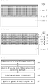
- FIG. 1-A is a diagram showing the inventive epitaxial wafer.
- the inventive epitaxial wafer 10 has a single crystal silicon layer 3 on a wafer 1 containing a group IV element including silicon, and has an oxygen atomic layer 2 between the single crystal silicon layer 3 and the wafer 1 containing the group IV element including silicon.
- the planar density of the oxygen in the oxygen atomic layer 2 that the inventive epitaxial wafer 10 has is 4 ⁇ 10 14 atoms/cm 2 or less.
- An epitaxial wafer having such a range has low stacking fault of the epitaxial layer of the single crystal silicon. Note that there is no lower limit to the planar density of the oxygen, and the planar density can be greater than 0.
- the wafer is a wafer 1 containing a group IV element including silicon, and for example, single crystal silicon, SiGe, or SiGeC may be used.
- the wafer 1 may be manufactured in any manner.
- a wafer manufactured by a Czochralski method hereinafter, referred to as a CZ method
- a wafer manufactured by a floating zone method hereinafter, referred to as an FZ method
- FIG. 1-B is a diagram showing the inventive epitaxial wafer having a plurality of oxygen atomic layers and single crystal silicon layers stacked alternately on a wafer.
- the present invention may have an oxygen atomic layer 2 and a single crystal silicon layer 3 alternately stacked repeatedly on a wafer 1 containing a group IV element including silicon.
- the uppermost surface is a single crystal silicon layer.
- the planar density of the oxygen in the oxygen atomic layer can be measured by SIMS (Secondary Ion Mass Spectrometry).
- SIMS Secondary Ion Mass Spectrometry
- a peak is formed at the depth where the Si oxide layer is formed.
- the planar density of the oxygen can be determined by adding up the product of a volume density in one sputtering and the depth near a peak.
- FIG. 2 is a diagram showing a flow of the inventive method for manufacturing an epitaxial wafer.
- S11 shows a step of providing a wafer containing a group IV element including silicon
- S12 shows a step of removing a natural oxide film in an atmosphere containing hydrogen
- S13 shows a step of forming an oxygen atomic layer
- S14 shows a step of forming a single crystal silicon by epitaxial growth, respectively.
- single crystal silicon, SiGe, or SiGeC can be used as the wafer containing a group IV element including silicon.
- the method for manufacturing the wafer is not particularly limited.
- a wafer manufactured by a CZ method may be used, or a wafer manufactured by an FZ method may be used.
- a single crystal silicon wafer is preferably used as the wafer containing a group IV element including silicon.
- a single crystal silicon wafer is used as the wafer containing a group IV element including silicon as described, versatility is enhanced.
- a wafer subjected to ion implantation and a heat treatment may be used as the silicon wafer.
- the step S12 of removing a natural oxide film in an atmosphere containing hydrogen according to the present invention is a step of removing a natural oxide film in a reducing dry process including hydrogen. According to studies by the present inventors, the removal of the natural oxide film is not sufficient or oxidization takes place immediately after the removal of the natural oxide film in conventional wet processes with HF, BHF, etc., and therefore, a single crystal silicon cannot be formed by epitaxial growth with stability.
- the natural oxide film is preferably removed by heating the wafer in the atmosphere containing hydrogen, and furthermore, the natural oxide film is more preferably removed by heating the wafer to a temperature in a range of 800°C or higher and 1250°C or lower and maintaining the temperature within the range for 1 second or more and 5 minutes or less.
- the natural oxide film can be removed more stably.
- the step of removing the natural oxide film it is also preferable to remove the natural oxide film by using plasma containing hydrogen.
- the natural oxide film When the natural oxide film is removed by using plasma containing hydrogen as described, the natural oxide film can be removed at a lower temperature than when the natural oxide film is removed by heating in an atmosphere containing hydrogen. Therefore, this is effective particularly when Ge and Sn, having low heat resistance, are contained in the wafer. For example, in the case of SiGe, the higher the proportion of Ge, the lower the heat-resistance temperature.
- the wafer when the natural oxide film is removed by using plasma containing hydrogen, the wafer may have the natural oxide film removed at room temperature, or may have the natural oxide film removed while heating.
- the planar density of the oxygen in the oxygen atomic layer is set to 4 ⁇ 10 14 atoms/cm 2 or less.
- the planar density is set within such a range, defects are not formed in the epitaxial layer. This is because crystallinity of the substrate is maintained when the oxidized amount (the planar density of the oxygen in the oxygen atomic layer) is small. Accordingly, there is no lower limit to the planar density of the oxygen, and the planar density can be greater than 0.
- the epitaxial layer is a polycrystalline silicon or an amorphous silicon. According to investigations of the present inventors, if the planar density of the oxygen in the oxygen atomic layer exceeds 4 ⁇ 10 14 atoms/cm 2 , defects are formed or amorphous silicon is formed.
- the time to expose the wafer to the atmosphere containing oxygen can be adjusted to form an oxygen atomic layer having the desired planar density of oxygen.
- the wafer is preferably oxidized in an atmosphere containing oxygen.
- the oxidization may be performed in an atmosphere having an oxygen concentration of 100%, or the oxidization may be performed in an atmosphere having an inert gas such as nitrogen, argon, helium, neon, krypton, and xenon mixed with oxygen. When an inert gas and oxygen are mixed, the atmosphere can be handled safely.
- the oxidization of the wafer may be performed at room temperature, or may be performed while heating.
- the wafer is preferably oxidized in the air.
- the oxidization can be performed easily without providing a facility for supplying an atmosphere containing oxygen.
- monosilane and disilane can be used, for example, as a gas used for the epitaxial growth of the single crystal silicon.
- Nitrogen and hydrogen may be used as a carrier gas.
- the pressure in the chamber can be a pressure at which a gas phase reaction does not occur.
- the epitaxial growth is preferably performed at a temperature of 450°C or higher and 800°C or lower.
- the film can be formed at a low temperature. In this manner, an epitaxial layer having the target thickness can be obtained easily by changing the growth temperature.
- Ge and Sn which have low heat resistance, are contained in the wafer, the film is desirably formed at a low temperature in order to prevent crystallinity from being degraded.
- an epitaxial growth apparatus a batch processing apparatus may be used, or a single wafer processing apparatus may be used.
- the step of forming the oxygen atomic layer by oxidizing the wafer and the step of forming the single crystal silicon by epitaxial growth can also be performed alternately multiple times.
- the gettering effect can be enhanced compared with when there is only one oxygen atomic layer.
- the inventive method for manufacturing an epitaxial wafer it is possible to introduce an oxygen atomic layer near an epitaxial layer stably and simply. Furthermore, the epitaxial wafer has an epitaxial layer of good-quality single crystal silicon.
- Hydrogen baking was performed in order to remove the natural oxide film of the prepared single crystal silicon wafer.
- the temperature was set to 1000°C, and the time was set to 1 minute. After that, the wafer was left to stand in the air for 4 hours to 6 hours to form an oxygen atomic layer.
- a single crystal silicon was formed by epitaxial growth at a temperature of 580°C on a surface of the single crystal silicon wafer having the oxygen atomic layer formed in the air.
- FIG. 3 shows the observation results.
- the planar density of the oxygen in the oxygen atomic layer was 1.4 ⁇ 10 14 atoms/cm 2 , 2.8 ⁇ 10 14 atoms/cm 2 , and 4.0 ⁇ 10 14 atoms/cm 2 , that is, 4 ⁇ 10 14 atoms/cm 2 or less, the single crystal silicon layer was formed without dislocation or stacking fault being formed in the epitaxial layer.
- Example 1 The same single crystal silicon wafer as those in Example 1 and Comparative Example 1 was prepared. After removing the natural oxide film by a wet process by HF cleaning, the wafer was left to stand in the air for 5 hours to form an oxygen atomic layer. Next, epitaxial growth was performed on a surface of the single crystal silicon wafer at a temperature of 580°C.
- the planar density of oxygen in the oxygen atomic layer of the wafer subjected to epitaxial growth was measured by SIMS, and in order to evaluate crystallinity, cross-sectional TEM observation was performed.
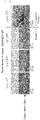
- FIG. 4 shows the observation results.
- the planar density of the oxygen in the oxygen atomic layer was 1.8 ⁇ 10 15 atoms/cm 2 , and as shown in FIG. 4 , on the oxygen atomic layer, a film of amorphous silicon was formed instead of single crystal silicon, and it was not possible to form a single crystal silicon. Note that if a heat treatment is performed on such a wafer after film formation, polysilicon is formed.
Landscapes
- Chemical & Material Sciences (AREA)
- Engineering & Computer Science (AREA)
- Materials Engineering (AREA)
- Metallurgy (AREA)
- Organic Chemistry (AREA)
- Crystallography & Structural Chemistry (AREA)
- Chemical Kinetics & Catalysis (AREA)
- General Chemical & Material Sciences (AREA)
- Mechanical Engineering (AREA)
- Physics & Mathematics (AREA)
- Plasma & Fusion (AREA)
- Inorganic Chemistry (AREA)
- Chemical Vapour Deposition (AREA)
- Recrystallisation Techniques (AREA)
Abstract
Description
- The present invention is a technology that relates to: a method for manufacturing an epitaxial wafer; and an epitaxial wafer.
- Silicon substrates that form semiconductor devices including solid-state image sensors and other transistors are required to have a gettering function against elements including heavy metal that cause the loss or degradation of device characteristics. For gettering, various techniques are proposed and put to practical use, for example: providing a polycrystalline silicon (Poly-Si) layer on a silicon substrate back surface; forming a damaged layer by blasting; using a silicon substrate having a high concentration of boron; and forming a precipitate. In gettering by oxide precipitation, gettering is performed by taking in a metal that has higher ionization tendency (lower electronegativity) than oxygen, which has high electronegativity.
- In addition, so-called proximity gettering, in which a gettering layer is formed in the vicinity of an active region of a device, is also proposed. Examples include a substrate having silicon formed by epitaxial growth on a substrate having carbon ion-implanted and so forth. In gettering, the element needs to diffuse to a gettering site (the metal bonds or clusters at the site rather than exists as a single element, so that the energy of the entire system is reduced), and the diffusion coefficient of a metal element contained in silicon varies depending on the element. Moreover, taking into consideration that metal cannot be diffused to gettering sites due to lower process temperatures in recent years, techniques of proximity gettering are proposed.
- If oxygen can be used in proximity gettering, it is considered that a silicon substrate having an extremely effective gettering layer can be achieved. In particular, in an epitaxial wafer having an oxygen atomic layer in an epitaxial layer, gettering of metallic impurities can be performed with certainty even in recent low-temperature processes.
- In the above, the use of oxygen in proximity gettering has been described regarding mainly the gettering of metallic impurities. As other advantageous effects of oxygen, an effect of preventing auto-doping during epitaxial growth by forming a CVD oxide film on a back surface is known, for example.
- Next, preceding technology will be referred to. The method described in
Patent Document 1 is a method in which, as the structure, a thin layer of oxygen is formed on silicon, and silicon is further grown. This method is a technique based on ALD ("Atomic layer deposition"). ALD is a method of adsorbing molecules that contain the target atoms and then detaching/desorbing unnecessary atoms (molecules) in the molecules. The method employs surface bonding and is very accurate. In addition, reaction control property is favorable, and the method is widely used. -
Patent Document 2 discloses a method of forming a natural oxide film on a silicon clean surface formed by vacuum heating or the like, and then adsorbing and depositing an oxide film or a different substance. -
Patent Documents 3 and 4 show that introducing a plurality of oxygen atomic layers into a silicon substrate makes it possible to improve device characteristics (enhance mobility). - Patent Document 5 shows a method of forming an epitaxial layer on an atomic layer having a thickness of 5 nm or less by using an SiH4 gas. In addition, Patent Document 5 shows a method of providing an oxygen atomic layer as the atomic layer and forming the oxygen atomic layer by using an oxygen gas.
- Patent Documents 6 and 7 disclose a method of forming an oxide film by bringing a surface of a semiconductor substrate into contact with oxidizing gas or an oxidizing solution, and then forming a single crystal silicon by epitaxial growth.
- An example in Patent Document 6 describes the removal of a natural oxide film by diluted hydrofluoric acid cleaning. In addition, the method of Patent Document 6 describes a method of allowing an oxidizing gas to flow and then allowing a silicon film-forming gas to flow.
-
Non Patent Document 1 shows a method of removing a natural oxide film by using HF, followed by oxidization in air, then forming a film of amorphous silicon by low pressure CVD, and subsequently forming an epitaxial layer of single crystal silicon by crystallization heat treatment. -
- Patent Document 1:
JP 2014-165494 A - Patent Document 2:
JP H05-243266 A - Patent Document 3:
US 7,153,763 B2 - Patent Document 4:
US 7,265,002 B2 - Patent Document 5:
JP 2019-004050 A - Patent Document 6:
JP 2008-263025 A - Patent Document 7:
JP 2009-016637 A - Non Patent Document 1: I. Mizushima et al., Jpn. J. Appl. Phys. 39(2000)2147.
- As described above, methods for the gettering of metallic impurities by forming a layer of oxygen in a wafer have been conventionally used. However, in conventional techniques, while a thin oxygen layer can be obtained with precision, there have been problems that the configuration of an apparatus is complicated, that there are many steps, and so forth.
- For example, in the technique disclosed in
Patent Document 1, single crystal silicon cannot be formed by epitaxial growth by ALD, so that at least two chambers for ALD and CVD are necessary, and there has been a problem that the configuration of the apparatus is complicated. In addition, since oxidization is performed with ozone, there has been a problem that a special generator for generating ozone is necessary. - Meanwhile, in the technique disclosed in Patent Document 5, there has been a problem that it is necessary to provide two chambers having separate exhaust systems in order to prevent SiH4 and oxygen from reacting and exploding.
- Meanwhile, in the technique disclosed in Patent Document 6, according to the investigation by the inventor, diluted hydrofluoric acid cleaning does not enable sufficient removal of the natural oxide film or oxidization takes place immediately after the removal of the natural oxide film, so that there has been a problem that it is difficult to form single crystal silicon by epitaxial growth stably. Moreover, there has been a problem that a special apparatus that takes safety into consideration is necessary in order to prevent the oxidizing gas and the silicon film-forming gas from reacting and exploding.
- In the method disclosed in
Non Patent Document 1, a heat treatment needs to be performed at the time of crystallization, and there has been a problem that the number of steps in the process is great. In addition, a large amount of hydrogen is generally contained in amorphous silicon, so that there is a possibility that defects caused by hydrogen may be formed during crystallization heat treatment. - In addition, in conventional technology, there have been problems that there is no description for introducing an oxygen layer stably or specific description for forming an epitaxial layer of good-quality single crystal silicon.
- For example, in
Patent Document 2, there is no description whatever regarding methods for forming an epitaxial layer of single crystal silicon on a wafer surface without causing dislocation or stacking fault. - Meanwhile, in
Patent Documents 3 and 4, there is no mention of specific methods for growing a silicon wafer having a plurality of oxygen atomic layers introduced. - Meanwhile, in Patent Documents 6 and 7, there is no description of methods for removing a natural oxide film before bringing into contact with oxidizing gas or an oxidizing solution.
- As described above, in conventional techniques, while a thin layer of oxygen can be obtained with precision, there have been problems that the configuration of the apparatus is complex, that the introduction of the oxygen layer is not stable, that an epitaxial layer of single crystal silicon having good quality cannot be obtained, and so forth. Therefore, a method for manufacturing an epitaxial wafer according to which an oxygen atomic layer can be introduced into an epitaxial layer stably and simply is needed.
- The present invention has been made in view of the above-described problems of conventional techniques. An object of the present invention is to provide a method for manufacturing an epitaxial wafer and an epitaxial wafer having an epitaxial layer of good-quality single crystal silicon while also allowing the introduction of an oxygen atomic layer in an epitaxial layer stably and simply.
- To achieve the object, the present invention provides a method for manufacturing an epitaxial wafer by forming a single crystal silicon layer on a wafer comprising a group IV element including silicon, the method comprising the steps of:
- removing a natural oxide film on a surface of the wafer comprising the group IV element including silicon in an atmosphere containing hydrogen;
- forming an oxygen atomic layer by oxidizing the wafer after removing the natural oxide film; and
- forming a single crystal silicon by epitaxial growth on the surface of the wafer after forming the oxygen atomic layer, wherein
- a planar density of oxygen in the oxygen atomic layer is set to 4×10¹⁴ atoms/cm2 or less.
- According to such a method for manufacturing an epitaxial wafer, it is possible to form single crystal silicon on a wafer simply and without forming dislocation or stacking fault on the oxygen atomic layer.
- In this event, a single crystal silicon wafer is preferably used as the wafer comprising the group IV element including silicon.
- Such a method for manufacturing an epitaxial wafer has higher versatility.
- In this event, the natural oxide film is preferably removed by heating the wafer in the atmosphere containing hydrogen in the step of removing the natural oxide film.
- When the natural oxide film is removed in this manner, the natural oxide film can be removed more effectively.
- In this event, the natural oxide film is preferably removed by heating the wafer to a temperature in a range of 800°C or higher and 1250°C or lower and maintaining the temperature within the range for 1 second or more and 5 minutes or less in the step of removing the natural oxide film.
- When temperature range and time are set thus in the step of removing the natural oxide film, the natural oxide film can be removed more stably.
- In this event, the natural oxide film is preferably removed by using plasma containing hydrogen in the step of removing the natural oxide film.
- When the natural oxide film is removed in this manner, the natural oxide film can be removed more effectively.
- In this event, the wafer is preferably oxidized in an atmosphere containing oxygen in the step of forming the oxygen atomic layer.
- By providing such an environment in the step of forming the oxygen atomic layer, the wafer can be oxidized more easily without providing special facilities.
- In this event, the wafer is preferably oxidized in air in the step of forming the oxygen atomic layer.
- By providing such an environment in the step of forming the oxygen atomic layer, the wafer can be oxidized more easily without providing special facilities.
- In this event, the epitaxial growth is preferably performed at a temperature of 450°C or higher and 800°C or lower in the step of forming the single crystal silicon by epitaxial growth.
- When such a temperature range is set in the step of forming the single crystal silicon by epitaxial growth, the epitaxial growth can be performed more stably and without defects being generated.
- In this event, the step of forming the oxygen atomic layer by oxidizing the wafer and the step of forming the single crystal silicon by epitaxial growth are preferably performed alternately multiple times.
- By providing a plurality of oxygen atomic layers in this manner, the gettering effect can be further enhanced compared with a case where there is one oxygen atomic layer.
- In addition, the present invention provides an epitaxial wafer comprising a single crystal silicon layer on a wafer comprising a group IV element including silicon, the epitaxial wafer comprising
- an oxygen atomic layer between the single crystal silicon layer and the wafer comprising the group IV element including silicon, wherein
- a planar density of oxygen in the oxygen atomic layer is 4×10¹⁴ atoms/cm2 or less.
- Such a wafer can have an extremely effective gettering layer in the vicinity of a device region. Therefore, the gettering of metallic impurities can be carried out with certainty even in low-temperature processes of recent years. Furthermore, the epitaxial wafer has an epitaxial layer of good-quality single crystal silicon.
- As described above, according to the inventive method for manufacturing an epitaxial wafer, it is possible to introduce an oxygen atomic layer near an epitaxial layer stably and simply. In addition, it is possible to provide a proximity gettering substrate that has a proximity gettering effect owing to the oxygen atomic layer and that has an epitaxial layer of single crystal silicon having good quality.
-
-
FIG. 1-A is a diagram showing the inventive epitaxial wafer. -
FIG. 1-B is a diagram showing the inventive epitaxial wafer having a plurality of oxygen atomic layers and single crystal silicon layers stacked alternately on a wafer. -
FIG. 2 is a diagram showing a flow of the inventive method for manufacturing an epitaxial wafer. -
FIG. 3 is a figure showing transmission electron microscope images of cross sections of the silicon substrates in Example 1 and Comparative Example 1. -
FIG. 4 is a figure showing transmission electron microscope images of a cross section of the silicon substrate in Comparative Example 2. - Hereinafter, the present invention will be described in detail, but the present invention is not limited thereto.
- As described above, there have been desired a method for manufacturing an epitaxial wafer and an epitaxial wafer according to which no special apparatuses or complicated processes are needed, and that have an oxygen atomic layer introduced into an epitaxial layer stably, while also having an epitaxial layer of good-quality single crystal silicon.
- The present inventors have earnestly studied the above-described problem and found out that it is possible to introduce an oxygen atomic layer to an epitaxial layer stably and simply without forming dislocation or stacking fault in the epitaxial layer on the oxygen atomic layer according to a method for manufacturing an epitaxial wafer by forming a single crystal silicon layer on a wafer containing a group IV element including silicon, the method including the steps of: removing a natural oxide film on a surface of the wafer containing the group IV element including silicon in an atmosphere containing hydrogen; forming an oxygen atomic layer by oxidizing the wafer after removing the natural oxide film; and forming a single crystal silicon by epitaxial growth on the surface of the wafer after forming the oxygen atomic layer, where a planar density of oxygen in the oxygen atomic layer is set to 4×10¹⁴ atoms/cm2 or less. Thus, the present invention has been completed.
- In addition, the present inventors have found out that an epitaxial wafer including a single crystal silicon layer on a wafer containing a group IV element including silicon, the epitaxial wafer including an oxygen atomic layer between the single crystal silicon layer and the wafer containing the group IV element including silicon, where a planar density of oxygen in the oxygen atomic layer is 4×10¹⁴ atoms/cm2 or less has an extremely effective gettering layer in the vicinity of a device region, so that the gettering of metallic impurities can be carried out with certainty even in low-temperature processes of recent years. In addition, the present inventors have found out that such an epitaxial wafer has an epitaxial layer of good-quality single crystal silicon. Thus, the present invention has been completed.
- Hereinafter, a description will be given with reference to the drawings.
-
FIG. 1-A is a diagram showing the inventive epitaxial wafer. Theinventive epitaxial wafer 10 has a singlecrystal silicon layer 3 on awafer 1 containing a group IV element including silicon, and has an oxygenatomic layer 2 between the singlecrystal silicon layer 3 and thewafer 1 containing the group IV element including silicon. - Here, the planar density of the oxygen in the oxygen
atomic layer 2 that theinventive epitaxial wafer 10 has is 4×10¹⁴ atoms/cm2 or less. An epitaxial wafer having such a range has low stacking fault of the epitaxial layer of the single crystal silicon. Note that there is no lower limit to the planar density of the oxygen, and the planar density can be greater than 0. - In the present invention, there are no particular limitations as long as the wafer is a
wafer 1 containing a group IV element including silicon, and for example, single crystal silicon, SiGe, or SiGeC may be used. - Here, the
wafer 1 may be manufactured in any manner. For example, a wafer manufactured by a Czochralski method (hereinafter, referred to as a CZ method) may be used, or a wafer manufactured by a floating zone method (hereinafter, referred to as an FZ method) may be used. Alternatively, it is also possible to use a wafer having a group IV element including silicon formed by epitaxial growth on a single crystal silicon wafer manufactured by a CZ method or an FZ method. - Meanwhile,
FIG. 1-B is a diagram showing the inventive epitaxial wafer having a plurality of oxygen atomic layers and single crystal silicon layers stacked alternately on a wafer. As shown inFIG. 1-B , the present invention may have an oxygenatomic layer 2 and a singlecrystal silicon layer 3 alternately stacked repeatedly on awafer 1 containing a group IV element including silicon. In this event, the uppermost surface is a single crystal silicon layer. - Here, the planar density of the oxygen in the oxygen atomic layer can be measured by SIMS (Secondary Ion Mass Spectrometry). When Si including an oxide layer is measured by SIMS, a peak is formed at the depth where the Si oxide layer is formed. The planar density of the oxygen can be determined by adding up the product of a volume density in one sputtering and the depth near a peak.
-
FIG. 2 is a diagram showing a flow of the inventive method for manufacturing an epitaxial wafer. S11 shows a step of providing a wafer containing a group IV element including silicon, S12 shows a step of removing a natural oxide film in an atmosphere containing hydrogen, S13 shows a step of forming an oxygen atomic layer, and S14 shows a step of forming a single crystal silicon by epitaxial growth, respectively. - In the present invention, for example, single crystal silicon, SiGe, or SiGeC can be used as the wafer containing a group IV element including silicon.
- Here, the method for manufacturing the wafer is not particularly limited. A wafer manufactured by a CZ method may be used, or a wafer manufactured by an FZ method may be used. Alternatively, it is also possible to use a wafer having a group IV element including silicon formed by epitaxial growth on a single crystal silicon wafer manufactured by a CZ method or an FZ method.
- In particular, a single crystal silicon wafer is preferably used as the wafer containing a group IV element including silicon.
- When a single crystal silicon wafer is used as the wafer containing a group IV element including silicon as described, versatility is enhanced. In this event, a wafer subjected to ion implantation and a heat treatment may be used as the silicon wafer.
- The step S12 of removing a natural oxide film in an atmosphere containing hydrogen according to the present invention is a step of removing a natural oxide film in a reducing dry process including hydrogen. According to studies by the present inventors, the removal of the natural oxide film is not sufficient or oxidization takes place immediately after the removal of the natural oxide film in conventional wet processes with HF, BHF, etc., and therefore, a single crystal silicon cannot be formed by epitaxial growth with stability.
- In the step of removing the natural oxide film, the natural oxide film is preferably removed by heating the wafer in the atmosphere containing hydrogen, and furthermore, the natural oxide film is more preferably removed by heating the wafer to a temperature in a range of 800°C or higher and 1250°C or lower and maintaining the temperature within the range for 1 second or more and 5 minutes or less.
- In this manner, the natural oxide film can be removed more stably.
- Furthermore, in the step of removing the natural oxide film, it is also preferable to remove the natural oxide film by using plasma containing hydrogen.
- When the natural oxide film is removed by using plasma containing hydrogen as described, the natural oxide film can be removed at a lower temperature than when the natural oxide film is removed by heating in an atmosphere containing hydrogen. Therefore, this is effective particularly when Ge and Sn, having low heat resistance, are contained in the wafer. For example, in the case of SiGe, the higher the proportion of Ge, the lower the heat-resistance temperature.
- Note that when the natural oxide film is removed by using plasma containing hydrogen, the wafer may have the natural oxide film removed at room temperature, or may have the natural oxide film removed while heating.
- In the step S13 of forming an oxygen atomic layer, the planar density of the oxygen in the oxygen atomic layer is set to 4×10¹⁴ atoms/cm2 or less. When the planar density is set within such a range, defects are not formed in the epitaxial layer. This is because crystallinity of the substrate is maintained when the oxidized amount (the planar density of the oxygen in the oxygen atomic layer) is small. Accordingly, there is no lower limit to the planar density of the oxygen, and the planar density can be greater than 0. If the oxidized amount is large, the epitaxial layer is a polycrystalline silicon or an amorphous silicon. According to investigations of the present inventors, if the planar density of the oxygen in the oxygen atomic layer exceeds 4×10¹⁴ atoms/cm2, defects are formed or amorphous silicon is formed.
- There are several methods for oxidizing a wafer, and in the present invention, for example, the time to expose the wafer to the atmosphere containing oxygen can be adjusted to form an oxygen atomic layer having the desired planar density of oxygen.
- In the step of forming the oxygen atomic layer, the wafer is preferably oxidized in an atmosphere containing oxygen.
- When the wafer is oxidized in such an environment, there is no need to provide special facilities, and the wafer can be oxidized easily. In addition, the oxidization may be performed in an atmosphere having an oxygen concentration of 100%, or the oxidization may be performed in an atmosphere having an inert gas such as nitrogen, argon, helium, neon, krypton, and xenon mixed with oxygen. When an inert gas and oxygen are mixed, the atmosphere can be handled safely. Furthermore, the oxidization of the wafer may be performed at room temperature, or may be performed while heating.
- In this case, the wafer is preferably oxidized in the air.
- When the step of forming the oxygen atomic layer is carried out in such an environment, the oxidization can be performed easily without providing a facility for supplying an atmosphere containing oxygen.
- In the step S14 of forming the single crystal silicon by epitaxial growth, monosilane and disilane can be used, for example, as a gas used for the epitaxial growth of the single crystal silicon. Nitrogen and hydrogen may be used as a carrier gas. In addition, the pressure in the chamber can be a pressure at which a gas phase reaction does not occur.
- In the step of forming the single crystal silicon by epitaxial growth, the epitaxial growth is preferably performed at a temperature of 450°C or higher and 800°C or lower.
- When such a temperature range is applied in the step of forming the single crystal silicon by epitaxial growth, dislocation and stacking fault can be prevented more effectively from being formed in the epitaxial layer. Since the higher the temperature, the higher the epitaxial growth rate, a thick epitaxial layer can be formed in a short time by forming the film at a high temperature. On the other hand, when it is desired to form a thin epitaxial layer, the film can be formed at a low temperature. In this manner, an epitaxial layer having the target thickness can be obtained easily by changing the growth temperature. In addition, when Ge and Sn, which have low heat resistance, are contained in the wafer, the film is desirably formed at a low temperature in order to prevent crystallinity from being degraded.
- In addition, as an epitaxial growth apparatus, a batch processing apparatus may be used, or a single wafer processing apparatus may be used.
- Furthermore, the step of forming the oxygen atomic layer by oxidizing the wafer and the step of forming the single crystal silicon by epitaxial growth can also be performed alternately multiple times.
- When a plurality of oxygen atomic layers are provided as described, the gettering effect can be enhanced compared with when there is only one oxygen atomic layer.
- As described above, according to the inventive method for manufacturing an epitaxial wafer, it is possible to introduce an oxygen atomic layer near an epitaxial layer stably and simply. Furthermore, the epitaxial wafer has an epitaxial layer of good-quality single crystal silicon.
- Hereinafter, the present invention will be described in detail with reference to an Example, but the present invention is not limited thereto.
- Single crystal silicon wafers each having the following conductivity type, diameter, and crystal plane orientation were prepared.
Conductivity type of substrate : p type Diameter : 300 mm Crystal plane orientation : (100) - Hydrogen baking was performed in order to remove the natural oxide film of the prepared single crystal silicon wafer. The temperature was set to 1000°C, and the time was set to 1 minute. After that, the wafer was left to stand in the air for 4 hours to 6 hours to form an oxygen atomic layer.
- Next, a single crystal silicon was formed by epitaxial growth at a temperature of 580°C on a surface of the single crystal silicon wafer having the oxygen atomic layer formed in the air.
- The planar density of oxygen in the oxygen atomic layer of the wafer subjected to epitaxial growth was measured by SIMS, and in order to evaluate crystallinity, cross-sectional TEM (Transmission Electron Microscopy) observation was performed.
FIG. 3 shows the observation results. As shown inFIG. 3 , in cases where the planar density of the oxygen in the oxygen atomic layer was 1.4×10¹⁴ atoms/cm2, 2.8×10¹⁴ atoms/cm2, and 4.0×10¹⁴ atoms/cm2, that is, 4×10¹⁴ atoms/cm2 or less, the single crystal silicon layer was formed without dislocation or stacking fault being formed in the epitaxial layer. - The production and evaluation of an epitaxial wafer were performed under the same conditions as in Example 1 except that in the formation of the oxygen atomic layer, the time that the wafer was left to stand in the air was set to 7 hours.
- As shown in
FIG. 3 , in the case where the planar density of the oxygen in the oxygen atomic layer was 4.8×10¹⁴ atoms/cm2, that is, greater than 4×10¹⁴ atoms/cm2, defects were formed. - The same single crystal silicon wafer as those in Example 1 and Comparative Example 1 was prepared. After removing the natural oxide film by a wet process by HF cleaning, the wafer was left to stand in the air for 5 hours to form an oxygen atomic layer. Next, epitaxial growth was performed on a surface of the single crystal silicon wafer at a temperature of 580°C.
- The planar density of oxygen in the oxygen atomic layer of the wafer subjected to epitaxial growth was measured by SIMS, and in order to evaluate crystallinity, cross-sectional TEM observation was performed.
FIG. 4 shows the observation results. The planar density of the oxygen in the oxygen atomic layer was 1.8×10¹⁵ atoms/cm2, and as shown inFIG. 4 , on the oxygen atomic layer, a film of amorphous silicon was formed instead of single crystal silicon, and it was not possible to form a single crystal silicon. Note that if a heat treatment is performed on such a wafer after film formation, polysilicon is formed. - It should be noted that the present invention is not limited to the above-described embodiments. The embodiments are just examples, and any examples that have substantially the same feature and demonstrate the same functions and effects as those in the technical concept disclosed in claims of the present invention are included in the technical scope of the present invention.
Claims (10)
- A method for manufacturing an epitaxial wafer by forming a single crystal silicon layer on a wafer comprising a group IV element including silicon, the method comprising the steps of:removing a natural oxide film on a surface of the wafer comprising the group IV element including silicon in an atmosphere containing hydrogen;forming an oxygen atomic layer by oxidizing the wafer after removing the natural oxide film; andforming a single crystal silicon by epitaxial growth on the surface of the wafer after forming the oxygen atomic layer, whereina planar density of oxygen in the oxygen atomic layer is set to 4×10¹⁴ atoms/cm2 or less.
- The method for manufacturing an epitaxial wafer according to claim 1, wherein a single crystal silicon wafer is used as the wafer comprising the group IV element including silicon.
- The method for manufacturing an epitaxial wafer according to claim 1 or 2, wherein the natural oxide film is removed by heating the wafer in the atmosphere containing hydrogen in the step of removing the natural oxide film.
- The method for manufacturing an epitaxial wafer according to claim 3, wherein the natural oxide film is removed by heating the wafer to a temperature in a range of 800°C or higher and 1250°C or lower and maintaining the temperature within the range for 1 second or more and 5 minutes or less in the step of removing the natural oxide film.
- The method for manufacturing an epitaxial wafer according to claim 1 or 2, wherein the natural oxide film is removed by using plasma containing hydrogen in the step of removing the natural oxide film.
- The method for manufacturing an epitaxial wafer according to any one of claims 1 to 5, wherein the wafer is oxidized in an atmosphere containing oxygen in the step of forming the oxygen atomic layer.
- The method for manufacturing an epitaxial wafer according to any one of claims 1 to 6, wherein the wafer is oxidized in air in the step of forming the oxygen atomic layer.
- The method for manufacturing an epitaxial wafer according to any one of claims 1 to 7, wherein the epitaxial growth is performed at a temperature of 450°C or higher and 800°C or lower in the step of forming the single crystal silicon by epitaxial growth.
- The method for manufacturing an epitaxial wafer according to any one of claims 1 to 8, wherein the step of forming the oxygen atomic layer by oxidizing the wafer and the step of forming the single crystal silicon by epitaxial growth are performed alternately multiple times.
- An epitaxial wafer comprising a single crystal silicon layer on a wafer comprising a group IV element including silicon, the epitaxial wafer comprisingan oxygen atomic layer between the single crystal silicon layer and the wafer comprising the group IV element including silicon, whereina planar density of oxygen in the oxygen atomic layer is 4×10¹⁴ atoms/cm2 or less.
Applications Claiming Priority (2)
| Application Number | Priority Date | Filing Date | Title |
|---|---|---|---|
| JP2020002741A JP7247902B2 (en) | 2020-01-10 | 2020-01-10 | Epitaxial wafer manufacturing method |
| PCT/JP2020/043540 WO2021140763A1 (en) | 2020-01-10 | 2020-11-24 | Epitaxial wafer manufacturing method and epitaxial wafer |
Publications (2)
| Publication Number | Publication Date |
|---|---|
| EP4089720A1 true EP4089720A1 (en) | 2022-11-16 |
| EP4089720A4 EP4089720A4 (en) | 2024-01-17 |
Family
ID=76787840
Family Applications (1)
| Application Number | Title | Priority Date | Filing Date |
|---|---|---|---|
| EP20911506.2A Pending EP4089720A4 (en) | 2020-01-10 | 2020-11-24 | METHOD FOR MANUFACTURING EPITAXIAL WAFER AND EPITAXIAL WAFER |
Country Status (7)
| Country | Link |
|---|---|
| US (1) | US20230028127A1 (en) |
| EP (1) | EP4089720A4 (en) |
| JP (1) | JP7247902B2 (en) |
| KR (1) | KR20220124696A (en) |
| CN (1) | CN114930500B (en) |
| TW (1) | TWI893031B (en) |
| WO (1) | WO2021140763A1 (en) |
Cited By (1)
| Publication number | Priority date | Publication date | Assignee | Title |
|---|---|---|---|---|
| EP4283024A4 (en) * | 2021-01-25 | 2024-12-04 | Shin-Etsu Handotai Co., Ltd. | METHOD FOR PRODUCING AN EPITATACTICAL WAFER |
Families Citing this family (5)
| Publication number | Priority date | Publication date | Assignee | Title |
|---|---|---|---|---|
| JP7740146B2 (en) * | 2022-07-06 | 2025-09-17 | 信越半導体株式会社 | Epitaxial wafer manufacturing method |
| CN119654700A (en) | 2022-08-08 | 2025-03-18 | 信越半导体株式会社 | Method for manufacturing silicon substrate for quantum computer, silicon substrate for quantum computer, and semiconductor device |
| JP2024168899A (en) * | 2023-05-25 | 2024-12-05 | 信越半導体株式会社 | High mobility substrate having .DELTA.-doped layer and method for manufacturing high mobility substrate |
| JP2025029308A (en) | 2023-08-21 | 2025-03-06 | 信越半導体株式会社 | Method for manufacturing epitaxial wafer |
| JP2025162887A (en) * | 2024-04-16 | 2025-10-28 | 信越半導体株式会社 | Measurement method for oxygen concentration of oxygen atom layer |
Family Cites Families (22)
| Publication number | Priority date | Publication date | Assignee | Title |
|---|---|---|---|---|
| US5422306A (en) | 1991-12-17 | 1995-06-06 | Matsushita Electric Industrial Co., Ltd. | Method of forming semiconductor hetero interfaces |
| DE69628505T2 (en) * | 1995-07-21 | 2004-05-06 | Canon K.K. | Semiconductor substrate and its manufacturing process |
| JP2000072595A (en) * | 1998-08-31 | 2000-03-07 | Shin Etsu Handotai Co Ltd | Single silicon crystal wafer doped with boron and epitaxial silicon wafer and their production |
| JP3478141B2 (en) * | 1998-09-14 | 2003-12-15 | 信越半導体株式会社 | Heat treatment method for silicon wafer and silicon wafer |
| US6346732B1 (en) * | 1999-05-14 | 2002-02-12 | Kabushiki Kaisha Toshiba | Semiconductor device with oxide mediated epitaxial layer |
| JP3886085B2 (en) | 1999-05-14 | 2007-02-28 | 株式会社東芝 | Manufacturing method of semiconductor epitaxial substrate |
| JP2003086569A (en) * | 2001-09-12 | 2003-03-20 | Tokyo Electron Ltd | Plasma processing method |
| US7153763B2 (en) | 2003-06-26 | 2006-12-26 | Rj Mears, Llc | Method for making a semiconductor device including band-engineered superlattice using intermediate annealing |
| AU2004300982B2 (en) | 2003-06-26 | 2007-10-25 | Mears Technologies, Inc. | Semiconductor device including MOSFET having band-engineered superlattice |
| JP2005109521A (en) | 2004-12-20 | 2005-04-21 | Sumitomo Mitsubishi Silicon Corp | Surface treatment method and silicon wafer |
| JP5168990B2 (en) | 2007-04-11 | 2013-03-27 | 信越半導体株式会社 | Manufacturing method of semiconductor substrate |
| JP5205840B2 (en) | 2007-07-06 | 2013-06-05 | 信越半導体株式会社 | Manufacturing method of semiconductor substrate |
| CN101971298A (en) * | 2007-11-02 | 2011-02-09 | 佳能安内华股份有限公司 | Surface treatment equipment and surface treatment method |
| JP2010045288A (en) * | 2008-08-18 | 2010-02-25 | Shin Etsu Handotai Co Ltd | Light-emitting element and manufacturing method thereof |
| JP2012114210A (en) * | 2010-11-24 | 2012-06-14 | Sumitomo Electric Ind Ltd | Method of manufacturing silicon carbide semiconductor device and manufacturing apparatus for silicon carbide semiconductor device |
| EP2770526B1 (en) | 2013-02-22 | 2018-10-03 | IMEC vzw | Oxygen monolayer on a semiconductor |
| JP6118757B2 (en) * | 2014-04-24 | 2017-04-19 | 信越半導体株式会社 | Manufacturing method of bonded SOI wafer |
| JP6861471B2 (en) * | 2015-06-12 | 2021-04-21 | キヤノン株式会社 | Imaging device and its manufacturing method and camera |
| JP6702268B2 (en) * | 2017-06-15 | 2020-05-27 | 信越半導体株式会社 | Epitaxial wafer manufacturing method |
| CN109509704B (en) * | 2017-09-15 | 2024-08-09 | 胜高股份有限公司 | Method for preparing epitaxial silicon wafer |
| JP6794977B2 (en) * | 2017-12-20 | 2020-12-02 | 株式会社Sumco | Manufacturing method of epitaxial silicon wafer and epitaxial silicon wafer |
| JP6844529B2 (en) | 2017-12-27 | 2021-03-17 | 株式会社Sumco | Epitaxial wafer manufacturing method and epitaxial wafer |
-
2020
- 2020-01-10 JP JP2020002741A patent/JP7247902B2/en active Active
- 2020-11-24 US US17/788,373 patent/US20230028127A1/en not_active Abandoned
- 2020-11-24 CN CN202080092094.3A patent/CN114930500B/en active Active
- 2020-11-24 KR KR1020227022164A patent/KR20220124696A/en active Pending
- 2020-11-24 WO PCT/JP2020/043540 patent/WO2021140763A1/en not_active Ceased
- 2020-11-24 EP EP20911506.2A patent/EP4089720A4/en active Pending
- 2020-12-10 TW TW109143646A patent/TWI893031B/en active
Cited By (1)
| Publication number | Priority date | Publication date | Assignee | Title |
|---|---|---|---|---|
| EP4283024A4 (en) * | 2021-01-25 | 2024-12-04 | Shin-Etsu Handotai Co., Ltd. | METHOD FOR PRODUCING AN EPITATACTICAL WAFER |
Also Published As
| Publication number | Publication date |
|---|---|
| JP7247902B2 (en) | 2023-03-29 |
| EP4089720A4 (en) | 2024-01-17 |
| CN114930500B (en) | 2025-12-05 |
| JP2021111696A (en) | 2021-08-02 |
| TW202130845A (en) | 2021-08-16 |
| CN114930500A (en) | 2022-08-19 |
| US20230028127A1 (en) | 2023-01-26 |
| KR20220124696A (en) | 2022-09-14 |
| WO2021140763A1 (en) | 2021-07-15 |
| TWI893031B (en) | 2025-08-11 |
Similar Documents
| Publication | Publication Date | Title |
|---|---|---|
| US20230028127A1 (en) | Method for manufacturing epitaxial wafer and epitaxial wafer | |
| US5607511A (en) | Method and apparatus for low temperature, low pressure chemical vapor deposition of epitaxial silicon layers | |
| US7651948B2 (en) | Pre-cleaning of substrates in epitaxy chambers | |
| EP4283024A1 (en) | Method for manufacturing epitaxial wafer | |
| US20050221591A1 (en) | Method of forming high-quality relaxed SiGe alloy layers on bulk Si substrates | |
| JP7740146B2 (en) | Epitaxial wafer manufacturing method | |
| JP7435516B2 (en) | Epitaxial wafer manufacturing method | |
| JP7347350B2 (en) | Method for setting epitaxial growth conditions and method for manufacturing epitaxial wafers | |
| JP2022125625A (en) | Manufacturing method for epitaxial wafer | |
| EP0259759B1 (en) | Method for low temperature, low pressure chemical vapor deposition of epitaxial silicon layers | |
| US7947552B2 (en) | Process for the simultaneous deposition of crystalline and amorphous layers with doping | |
| JP2822756B2 (en) | Vapor phase growth apparatus and thin film forming method thereof | |
| KR102966607B1 (en) | Method for manufacturing an epitaxial wafer | |
| US20250163606A1 (en) | Production method for single crystal semiconductor film, production method for multilayer film of single crystal semiconductor film, and semiconductor element | |
| JP2025029308A (en) | Method for manufacturing epitaxial wafer | |
| WO2025204274A1 (en) | Method for manufacturing epitaxial wafer | |
| CN118763138A (en) | Solar cell and method for manufacturing the same |
Legal Events
| Date | Code | Title | Description |
|---|---|---|---|
| STAA | Information on the status of an ep patent application or granted ep patent |
Free format text: STATUS: THE INTERNATIONAL PUBLICATION HAS BEEN MADE |
|
| PUAI | Public reference made under article 153(3) epc to a published international application that has entered the european phase |
Free format text: ORIGINAL CODE: 0009012 |
|
| STAA | Information on the status of an ep patent application or granted ep patent |
Free format text: STATUS: REQUEST FOR EXAMINATION WAS MADE |
|
| 17P | Request for examination filed |
Effective date: 20220623 |
|
| AK | Designated contracting states |
Kind code of ref document: A1 Designated state(s): AL AT BE BG CH CY CZ DE DK EE ES FI FR GB GR HR HU IE IS IT LI LT LU LV MC MK MT NL NO PL PT RO RS SE SI SK SM TR |
|
| DAV | Request for validation of the european patent (deleted) | ||
| DAX | Request for extension of the european patent (deleted) | ||
| REG | Reference to a national code |
Ref country code: DE Ref legal event code: R079 Free format text: PREVIOUS MAIN CLASS: H01L0021205000 Ipc: C23C0016020000 |
|
| A4 | Supplementary search report drawn up and despatched |
Effective date: 20231218 |
|
| RIC1 | Information provided on ipc code assigned before grant |
Ipc: H01L 21/02 20060101ALI20231212BHEP Ipc: C30B 29/06 20060101ALI20231212BHEP Ipc: C30B 25/18 20060101ALI20231212BHEP Ipc: C23C 16/24 20060101ALI20231212BHEP Ipc: C23C 16/02 20060101AFI20231212BHEP |