EP4086945A1 - Semiconductor structure and manufacturing method for same - Google Patents
Semiconductor structure and manufacturing method for same Download PDFInfo
- Publication number
- EP4086945A1 EP4086945A1 EP21865335.0A EP21865335A EP4086945A1 EP 4086945 A1 EP4086945 A1 EP 4086945A1 EP 21865335 A EP21865335 A EP 21865335A EP 4086945 A1 EP4086945 A1 EP 4086945A1
- Authority
- EP
- European Patent Office
- Prior art keywords
- connection layer
- layer
- semiconductor structure
- thermal expansion
- communication portion
- Prior art date
- Legal status (The legal status is an assumption and is not a legal conclusion. Google has not performed a legal analysis and makes no representation as to the accuracy of the status listed.)
- Pending
Links
Images





Classifications
-
- H—ELECTRICITY
- H10—SEMICONDUCTOR DEVICES; ELECTRIC SOLID-STATE DEVICES NOT OTHERWISE PROVIDED FOR
- H10W—GENERIC PACKAGES, INTERCONNECTIONS, CONNECTORS OR OTHER CONSTRUCTIONAL DETAILS OF DEVICES COVERED BY CLASS H10
- H10W20/00—Interconnections in chips, wafers or substrates
- H10W20/01—Manufacture or treatment
- H10W20/021—Manufacture or treatment of interconnections within wafers or substrates
- H10W20/023—Manufacture or treatment of interconnections within wafers or substrates the interconnections being through-semiconductor vias
-
- H—ELECTRICITY
- H10—SEMICONDUCTOR DEVICES; ELECTRIC SOLID-STATE DEVICES NOT OTHERWISE PROVIDED FOR
- H10W—GENERIC PACKAGES, INTERCONNECTIONS, CONNECTORS OR OTHER CONSTRUCTIONAL DETAILS OF DEVICES COVERED BY CLASS H10
- H10W20/00—Interconnections in chips, wafers or substrates
- H10W20/01—Manufacture or treatment
- H10W20/021—Manufacture or treatment of interconnections within wafers or substrates
- H10W20/023—Manufacture or treatment of interconnections within wafers or substrates the interconnections being through-semiconductor vias
- H10W20/0245—Manufacture or treatment of interconnections within wafers or substrates the interconnections being through-semiconductor vias comprising use of blind vias during the manufacture
-
- H—ELECTRICITY
- H10—SEMICONDUCTOR DEVICES; ELECTRIC SOLID-STATE DEVICES NOT OTHERWISE PROVIDED FOR
- H10W—GENERIC PACKAGES, INTERCONNECTIONS, CONNECTORS OR OTHER CONSTRUCTIONAL DETAILS OF DEVICES COVERED BY CLASS H10
- H10W20/00—Interconnections in chips, wafers or substrates
- H10W20/01—Manufacture or treatment
- H10W20/021—Manufacture or treatment of interconnections within wafers or substrates
- H10W20/023—Manufacture or treatment of interconnections within wafers or substrates the interconnections being through-semiconductor vias
- H10W20/0261—Manufacture or treatment of interconnections within wafers or substrates the interconnections being through-semiconductor vias characterised by the filling method or the material of the conductive fill
-
- H—ELECTRICITY
- H10—SEMICONDUCTOR DEVICES; ELECTRIC SOLID-STATE DEVICES NOT OTHERWISE PROVIDED FOR
- H10W—GENERIC PACKAGES, INTERCONNECTIONS, CONNECTORS OR OTHER CONSTRUCTIONAL DETAILS OF DEVICES COVERED BY CLASS H10
- H10W20/00—Interconnections in chips, wafers or substrates
- H10W20/01—Manufacture or treatment
- H10W20/021—Manufacture or treatment of interconnections within wafers or substrates
- H10W20/023—Manufacture or treatment of interconnections within wafers or substrates the interconnections being through-semiconductor vias
- H10W20/0265—Manufacture or treatment of interconnections within wafers or substrates the interconnections being through-semiconductor vias characterised by the sidewall insulation
-
- H—ELECTRICITY
- H10—SEMICONDUCTOR DEVICES; ELECTRIC SOLID-STATE DEVICES NOT OTHERWISE PROVIDED FOR
- H10W—GENERIC PACKAGES, INTERCONNECTIONS, CONNECTORS OR OTHER CONSTRUCTIONAL DETAILS OF DEVICES COVERED BY CLASS H10
- H10W20/00—Interconnections in chips, wafers or substrates
- H10W20/01—Manufacture or treatment
- H10W20/071—Manufacture or treatment of dielectric parts thereof
- H10W20/074—Manufacture or treatment of dielectric parts thereof of dielectric parts comprising thin functional dielectric layers, e.g. dielectric etch-stop, barrier, capping or liner layers
- H10W20/076—Manufacture or treatment of dielectric parts thereof of dielectric parts comprising thin functional dielectric layers, e.g. dielectric etch-stop, barrier, capping or liner layers in via holes or trenches
-
- H—ELECTRICITY
- H10—SEMICONDUCTOR DEVICES; ELECTRIC SOLID-STATE DEVICES NOT OTHERWISE PROVIDED FOR
- H10W—GENERIC PACKAGES, INTERCONNECTIONS, CONNECTORS OR OTHER CONSTRUCTIONAL DETAILS OF DEVICES COVERED BY CLASS H10
- H10W20/00—Interconnections in chips, wafers or substrates
- H10W20/20—Interconnections within wafers or substrates, e.g. through-silicon vias [TSV]
-
- H—ELECTRICITY
- H10—SEMICONDUCTOR DEVICES; ELECTRIC SOLID-STATE DEVICES NOT OTHERWISE PROVIDED FOR
- H10W—GENERIC PACKAGES, INTERCONNECTIONS, CONNECTORS OR OTHER CONSTRUCTIONAL DETAILS OF DEVICES COVERED BY CLASS H10
- H10W20/00—Interconnections in chips, wafers or substrates
- H10W20/20—Interconnections within wafers or substrates, e.g. through-silicon vias [TSV]
- H10W20/211—Through-semiconductor vias, e.g. TSVs
- H10W20/213—Cross-sectional shapes or dispositions
- H10W20/2134—TSVs extending from the semiconductor wafer into back-end-of-line layers
-
- H—ELECTRICITY
- H10—SEMICONDUCTOR DEVICES; ELECTRIC SOLID-STATE DEVICES NOT OTHERWISE PROVIDED FOR
- H10W—GENERIC PACKAGES, INTERCONNECTIONS, CONNECTORS OR OTHER CONSTRUCTIONAL DETAILS OF DEVICES COVERED BY CLASS H10
- H10W20/00—Interconnections in chips, wafers or substrates
- H10W20/40—Interconnections external to wafers or substrates, e.g. back-end-of-line [BEOL] metallisations or vias connecting to gate electrodes
- H10W20/41—Interconnections external to wafers or substrates, e.g. back-end-of-line [BEOL] metallisations or vias connecting to gate electrodes characterised by their conductive parts
- H10W20/42—Vias, e.g. via plugs
-
- H—ELECTRICITY
- H10—SEMICONDUCTOR DEVICES; ELECTRIC SOLID-STATE DEVICES NOT OTHERWISE PROVIDED FOR
- H10W—GENERIC PACKAGES, INTERCONNECTIONS, CONNECTORS OR OTHER CONSTRUCTIONAL DETAILS OF DEVICES COVERED BY CLASS H10
- H10W20/00—Interconnections in chips, wafers or substrates
- H10W20/40—Interconnections external to wafers or substrates, e.g. back-end-of-line [BEOL] metallisations or vias connecting to gate electrodes
- H10W20/41—Interconnections external to wafers or substrates, e.g. back-end-of-line [BEOL] metallisations or vias connecting to gate electrodes characterised by their conductive parts
- H10W20/44—Conductive materials thereof
- H10W20/4403—Conductive materials thereof based on metals, e.g. alloys, metal silicides
- H10W20/4421—Conductive materials thereof based on metals, e.g. alloys, metal silicides the principal metal being copper
-
- H—ELECTRICITY
- H10—SEMICONDUCTOR DEVICES; ELECTRIC SOLID-STATE DEVICES NOT OTHERWISE PROVIDED FOR
- H10W—GENERIC PACKAGES, INTERCONNECTIONS, CONNECTORS OR OTHER CONSTRUCTIONAL DETAILS OF DEVICES COVERED BY CLASS H10
- H10W20/00—Interconnections in chips, wafers or substrates
- H10W20/40—Interconnections external to wafers or substrates, e.g. back-end-of-line [BEOL] metallisations or vias connecting to gate electrodes
- H10W20/41—Interconnections external to wafers or substrates, e.g. back-end-of-line [BEOL] metallisations or vias connecting to gate electrodes characterised by their conductive parts
- H10W20/44—Conductive materials thereof
- H10W20/4462—Carbon or carbon-containing materials, e.g. graphene
-
- H—ELECTRICITY
- H10—SEMICONDUCTOR DEVICES; ELECTRIC SOLID-STATE DEVICES NOT OTHERWISE PROVIDED FOR
- H10W—GENERIC PACKAGES, INTERCONNECTIONS, CONNECTORS OR OTHER CONSTRUCTIONAL DETAILS OF DEVICES COVERED BY CLASS H10
- H10W40/00—Arrangements for thermal protection or thermal control
- H10W40/20—Arrangements for cooling
- H10W40/25—Arrangements for cooling characterised by their materials
Definitions
- the present disclosure relates to the technical field of semiconductors, and in particular to a semiconductor structure and a manufacturing method thereof.
- a metal conductive material filled in a communication portion may affect the lattice around the communication portion during thermal expansion, thus affecting the performance of the semiconductor structure.
- the present disclosure provides a semiconductor structure and a manufacturing method thereof, to improve the performance of the semiconductor structure.
- a semiconductor structure including:
- a semiconductor structure including:
- a method of manufacturing a semiconductor structure including:
- the semiconductor structure of the present disclosure includes a substrate and a communication portion, the communication portion including a first connection layer, a second connection layer, and a third connection layer that are made of different conductive materials; thermal expansion coefficients of the second connection layer and the third connection layer are both less than a thermal expansion coefficient of the first connection layer. That is, the second connection layer and the third connection layer change little under thermal expansion, thereby reducing the impact on the lattice around the communication portion, thus improving the performance of the semiconductor structure.
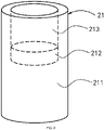
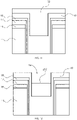
- the semiconductor structure includes: a base 10; and a communication portion 21, the communication portion 21 being located in the base 10, the communication portion 21 including a first connection layer 211, a second connection layer 212, and a third connection layer 213, the second connection layer 212 being located on the first connection layer 211, and the third connection layer 213 being located on the second connection layer 212; wherein the first connection layer 211, the second connection layer 212, and the third connection layer 213 include different conductive materials; thermal expansion coefficients of the second connection layer 212 and the third connection layer 213 are both less than a thermal expansion coefficient of the first connection layer 211.
- the semiconductor structure in an embodiment of the present disclosure includes a substrate 10 and a communication portion 21, wherein the communication portion 21 includes a first connection layer 211, a second connection layer 212, and a third connection layer 213 that are made of different conductive materials; thermal expansion coefficients of the second connection layer 212 and the third connection layer 213 are both less than a thermal expansion coefficient of the first connection layer 211. That is, the second connection layer 212 and the third connection layer 213 change little under thermal expansion, thereby reducing the impact on the lattice around the communication portion 21, thus improving the performance of the semiconductor structure.
- the thermal expansion coefficients of the second connection layer 212 and the third connection layer 213 are both less than the thermal expansion coefficient of the first connection layer 211, a material with a low thermal expansion coefficient is used as part of the conductive materials of the communication portion 21, to reduce the impact of metal thermal expansion on an active element region, and also reduce electrical changes of MOS elements in the peripheral lattice, thus reducing the size of the chip design.
- the second connection layer 212 and the third connection layer 213, which have lower thermal expansion coefficients, are deformed less under heat, thus avoiding squeezing the lattice around the communication portion 21 with a high pressure, thereby avoiding the impact on other components in the base 10.
- the communication portion 21 is a part of a conductive portion 20.
- the conductive portion 20 further includes a first conductive layer 22.
- the first conductive layer 22 is located above the communication portion 21, and the third connection layer 213 is connected to the first conductive layer 22. Because the second connection layer 212 and the third connection layer 213 are close to the first conductive layer 22, and the thermal expansion coefficients of the second connection layer 212 and the third connection layer 213 are relatively low, the first conductive layer 22 is not excessively squeezed.
- the communication portion 21 is a through-silicon via.
- the thermal expansion coefficient of the second connection layer 212 is less than the thermal expansion coefficient of the third connection layer 213. That is, in the communication portion 21, the conductive material with the lowest thermal expansion coefficient is located in the middle position.
- the base 10 is generally provided with a large number of components at a position corresponding to this middle position. Therefore, the conductive material with the lowest thermal expansion coefficient is subject to the smallest impact of thermal expansion, and basically will not squeeze components.
- the second connection layer 212 or the third connection layer 213 includes graphene
- the first connection layer 211 includes copper.
- Copper has a higher thermal expansion coefficient. However, since copper is arranged at the bottom, it does not affect the components in the base 10.
- the second connection layer 212 or the third connection layer 213 is closer to the components in the base 10, and graphene has a negative thermal expansion coefficient. Therefore, graphene can offset the thermal expansion of copper, thus avoiding the problem of squeezing.
- the first connection layer 211 is made of copper
- the second connection layer 212 is made of graphene
- the third connection layer 213 is made of tungsten.
- connection layer 212 when the second connection layer 212 includes graphene, which is sandwiched between the first connection layer 211 and the third connection layer 213, graphene that has a certain thermal storage function can absorb heat from the conductive materials with the higher thermal expansion coefficients, that is, absorb heat from the first connection layer 211 and the third connection layer 213, thereby reducing thermal expansion of other conductive materials.
- connection layer 212 includes graphene
- heat generated by the first connection layer 211 and the second connection layer 212 can be transferred to the first conductive layer 22 via graphene in time, and transmitted out through a structure connected to the first conductive layer 22, thereby achieving the effect of rapid heat dissipation.
- the second connection layer 212 is located in the first connection layer 211, that is, the second connection layer 212 is peripherally surrounded by the first connection layer 211.
- the first connection layer 211 with the higher thermal expansion coefficient can protect the second connection layer 212.
- the second connection layer 212 will not generate a large squeezing force due to thermal expansion.
- the second connection layer 212 is located in the first connection layer 211; the bottom of the third connection layer 213 is flush with the top of the second connection layer 212 and the top of the first connection layer 211.
- the second connection layer 212 is located in the first connection layer 211
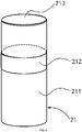
- the third connection layer 213 is located in the first connection layer 211. That is, the second connection layer 212 and the third connection layer 213 are both peripherally surrounded by the first connection layer 211, specifically as shown in FIG. 1 and FIG. 2 .
- projection of the second connection layer 212 coincides with projection of the third connection layer 213, that is, a cross sectional area of the second connection layer 212 is equal to a cross section of the third connection layer 213.
- the top of the third connection layer 213 is flush with the top of the first connection layer 211.
- a groove is formed in the first connection layer 211.
- the second connection layer 212 and the third connection layer 213 are located in the groove, and the top of the first connection layer 211 and the top of the third connection layer 213 are connected to the first conductive layer 22, specifically as shown in FIG. 1 and FIG. 2 .
- the first connection layer 211, the second connection layer 212, and the third connection layer 213 include different conductive materials.
- the thermal expansion coefficient of the second connection layer 212 is less than the thermal expansion coefficient of the third connection layer 213, and the thermal expansion coefficient of the third connection layer 213 is less than the thermal expansion coefficient of the first connection layer 211.
- the first connection layer 211 is made of copper
- the second connection layer 212 is made of graphene
- the third connection layer 213 is made of tungsten.
- first connection layer 211, the second connection layer 212, and projection of the third connection layer 213 coincide with each other. That is, the first connection layer 211, the second connection layer 212, and the third connection layer 213 are sequentially stacked along a height direction of the base 10, and the cross sectional area of the first connection layer 211, the cross sectional area of the second connection layer 212, and the cross sectional area of the third connection layer 213 are equal. In this case, only the third connection layer 213 is directly connected to the first conductive layer 22.
- the first connection layer 211, the second connection layer 212, and the third connection layer 213 include different conductive materials.
- the thermal expansion coefficient of the second connection layer 212 is less than the thermal expansion coefficient of the third connection layer 213, and the thermal expansion coefficient of the third connection layer 213 is less than the thermal expansion coefficient of the first connection layer 211.
- the first connection layer 211 is made of copper
- the second connection layer 212 is made of graphene
- the third connection layer 213 is made of tungsten.
- the second connection layer 212 is located in the first connection layer 211, and in the direction perpendicular to the base 10, projection of the first connection layer 211 coincides with projection of the third connection layer 213. That is, the bottom of the third connection layer 213 is flush with the top of the second connection layer 212 and the top of the first connection layer 211.
- the base 10 includes: a silicon substrate 11, the bottom of the second connection layer 212 being lower than an upper surface of the silicon substrate 11; and an insulation layer 12, the insulation layer 12 covers the upper surface of the silicon substrate 11 and covers an outer surface of the communication portion 21, and the first conductive layer 22 is located in the insulation layer 12.
- the base 10 includes the silicon substrate 11 and the insulation layer 12.
- the communication portion 21 is partially located in the silicon substrate 11; the bottom of the second connection layer 212 is lower than the upper surface of the silicon substrate 11, and the thermal expansion coefficient of the second connection layer 212 is less than the thermal expansion coefficient of the first connection layer 211. Therefore, the second connection layer 212 will not be expanded excessively under heat, thereby avoiding the impact on a part of the silicon substrate 11 which is close to the upper surface of the second connection layer 212.
- a functional layer 111 is formed in the silicon substrate 11, and the bottom of the second connection layer 212 is lower than a lower surface of the functional layer 111. That is, a total height of the second connection layer 212 and the third connection layer 213 is not less than a height of the functional layer 111 in the silicon substrate 11, thereby avoiding squeezing the functional layer 111 under thermal expansion.
- the height of the second connection layer 212 may be greater than the height of the functional layer 111.
- various components may be provided in the functional layer 111. Types of the components are not limited herein, and can be selected according to the actual needs. The focus herein is that the second connection layer 212, after overall thermal expansion, will not squeeze the functional layer 111, thereby protecting the functional layer 111.
- the top of the second connection layer 212 is higher than the upper surface of the silicon substrate 11. That is, the height of the second connection layer 212 may be greater than the height of the functional layer 111, thereby protecting the part of the silicon substrate 11 which is close to the insulation layer 12, and avoiding squeezing the functional layer 111.
- first connection layer 211, the second connection layer 212, and the third connection layer 213 may be columnar structures.
- the second connection layer 212 may have a diameter of 200 nm to 10 um and a depth of 1 um to 20 um. A portion of the second connection layer 212 which enters the silicon substrate 11 has a depth greater than or equal to 1 um.
- the silicon substrate 11 may be made of a silicon-containing material.
- the silicon substrate 11 may be made of any suitable material, including, for example, at least one of silicon, monocrystalline silicon, amorphous silicon, silicon-germanium, monocrystalline silicon-germanium, silicon carbide, or sapphire.
- the insulation layer 12 may include silicon dioxide (SiO 2 ), silicon oxide carbon (SiOC), silicon nitride (SiN), silicon carbon nitride (SiCN), and other related integrated-circuit insulation materials.
- the semiconductor structure further includes: a second conductive layer 30, the second conductive layer 30 being located in the base 10, the second conductive layer 30 is spaced apart from the first conductive layer 22 and is located above the first conductive layer 22, the first conductive layer 22 is connected to the second conductive layer 30 through connection pillars 31, and the connection pillars 31 are conductive structures.
- An embodiment of the present disclosure further provides a semiconductor structure, including: a base 10; and a communication portion 21, the communication portion 21 being located in the base 10, the communication portion 21 includes a first connection layer 211, a second connection layer 212, and a third connection layer 213, the second connection layer 212 being located on the first connection layer 211, and the third connection layer 213 being located on the second connection layer 212; the second connection layer 212 and the third connection layer 213 both include graphene, and thermal expansion coefficients of the second connection layer 212 and the third connection layer 213 are both less than a thermal expansion coefficient of the first connection layer 211.
- the semiconductor structure in this embodiment includes the first connection layer 211 and graphene located above the first connection layer 211, graphene can effectively avoid impact on the lattice around the communication portion 21, and heat can be transmitted out in time through graphene. In this way, the performance of the semiconductor structure is improved.
- An embodiment of the present disclosure further provides a method of manufacturing a semiconductor structure.
- the method of manufacturing a semiconductor structure includes:
- the first connection layer 211, the second connection layer 212, and the third connection layer 213 include different conductive materials; thermal expansion coefficients of the second connection layer 212 and the third connection layer 213 are both less than a thermal expansion coefficient of the first connection layer 211.
- a communication portion 21 is formed on a matrix 13, the communication portion 21 including a first connection layer 211, a second connection layer 212, and a third connection layer 213 that are made of different conductive materials; thermal expansion coefficients of the second connection layer 212 and the third connection layer 213 are both less than a thermal expansion coefficient of the first connection layer 211, and the third connection layer 213 is connected to a first conductive layer 22. That is, the second connection layer 212 and the third connection layer 213 change little under thermal expansion, thereby reducing the impact on the lattice around the communication portion 21, thus improving the performance of the semiconductor structure.
- the second connection layer 212 or the third connection layer 213 includes graphene
- the first connection layer 211 includes copper.
- Copper has a higher thermal expansion coefficient. However, since copper is arranged at the bottom, it does not affect the components be the base 10.
- the second connection layer 212 or the third connection layer 213 is closer to the components in the base 10, and graphene has a negative thermal expansion coefficient. Therefore, graphene can offset the thermal expansion of copper, thus avoiding the problem of squeezing.
- an opening 14 is formed in the first connection layer 211; the second connection layer 212 and the third connection layer 213 are sequentially formed in the opening 14, that is, the structure shown in FIG. 1 and FIG. 2 is formed.
- the matrix 13 includes a silicon substrate 11 and a first insulation layer 15.
- a hole 16 is formed in the silicon substrate 11 and the first insulation layer 15; the hole 16 penetrates the first insulation layer 15 but does not necessarily penetrate the silicon substrate 11, which is not limited herein.
- a second insulation layer 17 is covered on the first insulation layer 15, and the second insulation layer 17 covers the wall of the hole 16, as shown in FIG. 8 .
- a third insulation layer 18 is covered on the second insulation layer 17, and the third insulation layer 18 covers an upper surface and side surfaces of the second insulation layer 17, as shown in FIG. 9 .
- a first initial connection layer 19 is covered on the third insulation layer 18; the first initial connection layer 19 fills part of the hole 16, and an opening 14 is formed above the first initial connection layer 19, as shown in FIG. 10
- a second initial connection layer 32 is covered on the first initial connection layer 19, and the second initial connection layer 32 fills the opening 14, as shown in FIG. 11 .
- a third initial connection layer 33 is covered on the first initial connection layer 19, and the third initial connection layer 33 fills the opening 14, as shown in FIG. 13 .
- the third initial connection layer 33 which covers the upper surface of the first initial connection layer 19 and is located on the outer side of the opening 14, and a part of the first initial connection layer 19 which is located on the third insulation layer 18 are removed, to form the first connection layer 211 and the third connection layer 213, as shown in FIG. 14 . That is, the semiconductor structure shown in FIG. 1 can be finally formed.
- the first connection layer 211, the second connection layer 212, and the third connection layer 213 are sequentially formed in the matrix 13. In a direction perpendicular to the matrix 13, projection of the first connection layer 211, projection of the second connection layer 212, and projection of the third connection layer 213 coincide with each other. That is, the structure shown in FIG. 3 and FIG. 4 is formed.
- part of the first initial connection layer 19 is removed, that is, an area above the hole 16 is exposed, to form the first connection layer 211, as shown in FIG. 15 .
- a second initial connection layer 32 is covered on the third insulation layer 18, and the second initial connection layer 32 fills the hole 16, as shown in FIG. 16 .
- the second initial connection layer 32 is partially removed, that is, an area above the hole 16 is exposed, to form the second connection layer 212, as shown in FIG. 17 .
- a third initial connection layer 33 is covered on the third insulation layer 18, and the third initial connection layer 33 fills the hole 16, as shown in FIG. 18 .
- the third initial connection layer 33 is partially removed, that is, an upper surface of the third initial connection layer 33 is made to be flush with an upper surface of the third insulation layer 18, to form the third connection layer 213, as shown in FIG. 19 . That is, the semiconductor structure shown in FIG. 3 can be finally formed.
- the first insulation layer 15, the second insulation layer 17, and the third insulation layer 18 may include silicon dioxide (SiO 2 ), silicon oxide carbon (SiOC), silicon nitride (SiN), silicon carbon nitride (SiCN), and other related integrated-circuit insulation materials.
- a formation process of the first insulation layer 15, the second insulation layer 17, the third insulation layer 18, the second initial connection layer 32, and the third initial connection layer 33 can be selected from a group consisting of a physical vapor deposition (PVD) process, a chemical vapor deposition (CVD) process, an atomic layer deposition (ALD) process, an in-situ steam generation (ISSG) process, and a spin on dielectric (SOD) process, etc., which is not limited herein.
- PVD physical vapor deposition
- CVD chemical vapor deposition
- ALD atomic layer deposition
- ISSG in-situ steam generation
- SOD spin on dielectric
- the formation process of the opening 14 and the hole 16 includes lithography and etching. After each coating is formed, a chemical mechanical polishing (CMP) process can be performed to ensure the flatness of the coating.
- CMP chemical mechanical polishing
- the first initial connection layer 19 can be formed by a process such as electroplating or sputtering, which is not limited therein.
- the semiconductor structure can be formed by using the foregoing method of manufacturing a semiconductor structure.
- the method of manufacturing a semiconductor structure can further include forming a second conductive layer 30, and the like, which is not limited herein.
- the silicon substrate 11 and the various insulation layers described above are all part of the base 10, that is, the matrix 13 is a part of the base 10.
- the first insulation layer 15, the second insulation layer 17, and the third insulation layer 18 are all part of the insulation layer 12.
Landscapes
- Internal Circuitry In Semiconductor Integrated Circuit Devices (AREA)
- Metal-Oxide And Bipolar Metal-Oxide Semiconductor Integrated Circuits (AREA)
- Thin Film Transistor (AREA)
Abstract
Description
- The present disclosure claims the priority to
Chinese Patent Application 202110265111.5, titled "SEMICONDUCTOR STRUCTURE AND MANUFACTURING METHOD THEREOF", filed on March 10, 2021 - The present disclosure relates to the technical field of semiconductors, and in particular to a semiconductor structure and a manufacturing method thereof.
- In the prior art, a metal conductive material filled in a communication portion may affect the lattice around the communication portion during thermal expansion, thus affecting the performance of the semiconductor structure.
- The present disclosure provides a semiconductor structure and a manufacturing method thereof, to improve the performance of the semiconductor structure.
- According to a first aspect of the present disclosure, a semiconductor structure is provided, including:
- a substrate;
- a communication portion, the communication portion being located in the substrate and the communication portion including a first connection layer, a second connection layer, and a third connection layer, the second connection layer being located on the first connection layer, and the third connection layer being located on the second connection layer;
- wherein the first connection layer, the second connection layer, and the third connection layer include different conductive materials, and thermal expansion coefficients of the second connection layer and the third connection layer are both less than a thermal expansion coefficient of the first connection layer.
- According to a second aspect of the present disclosure, a semiconductor structure is provided, including:
- a substrate;
- a communication portion, the communication portion being located in the substrate and the communication portion including a first connection layer, a second connection layer, and a third connection layer, the second connection layer being located on the first connection layer, and the third connection layer being located on the second connection layer;
- wherein the second connection layer and the third connection layer both include graphene, and thermal expansion coefficients of the second connection layer and the third connection layer are both less than a thermal expansion coefficient of the first connection layer.
- According to a third aspect of the present disclosure, a method of manufacturing a semiconductor structure is provided, including:
- providing a matrix; and
- forming a communication portion on the matrix, the communication portion including a first connection layer, a second connection layer, and a third connection layer, the second connection layer being formed on the first connection layer, and the third connection layer being formed on the second connection layer;
- wherein the first connection layer, the second connection layer, and the third connection layer include different conductive materials, and thermal expansion coefficients of the second connection layer and the third connection layer are both less than a thermal expansion coefficient of the first connection layer.
- The semiconductor structure of the present disclosure includes a substrate and a communication portion, the communication portion including a first connection layer, a second connection layer, and a third connection layer that are made of different conductive materials; thermal expansion coefficients of the second connection layer and the third connection layer are both less than a thermal expansion coefficient of the first connection layer. That is, the second connection layer and the third connection layer change little under thermal expansion, thereby reducing the impact on the lattice around the communication portion, thus improving the performance of the semiconductor structure.
- The preferred embodiments of the present disclosure are described in detail below with reference to the accompanying drawings to make the objectives, features and advantages of the present disclosure more obvious. The drawings are merely exemplary illustrations of the present disclosure, and are not necessarily drawn to scale. The same reference numerals in the drawings always represent the same parts. In the drawings:
-
FIG. 1 is a schematic structural diagram of a semiconductor structure according to a first exemplary implementation; -
FIG. 2 is a schematic structural diagram of a communication portion of the semiconductor structure according to the first exemplary implementation; -
FIG. 3 is a schematic structural diagram of a semiconductor structure according to a second exemplary implementation; -
FIG. 4 is a schematic structural diagram of a communication portion of the semiconductor structure according to the second exemplary implementation; -
FIG. 5 is a schematic structural diagram of a semiconductor structure according to a third exemplary implementation; -
FIG. 6 is a schematic flowchart of a method of manufacturing a semiconductor structure according to an exemplary implementation; -
FIG. 7 is a schematic structural diagram of forming a hole in a method of manufacturing a semiconductor structure according to a first exemplary implementation; -
FIG. 8 is a schematic structural diagram of forming a hole in a second insulation layer in the method of manufacturing a semiconductor structure according to the first exemplary implementation; -
FIG. 9 is a schematic structural diagram of forming a hole in a third insulation layer in the method of manufacturing a semiconductor structure according to the first exemplary implementation; -
FIG. 10 is a schematic structural diagram of forming a first initial connection layer in the method of manufacturing a semiconductor structure according to the first exemplary implementation; -
FIG. 11 is a schematic structural diagram of forming a second initial connection layer in the method of manufacturing a semiconductor structure according to the first exemplary implementation; -
FIG. 12 is a schematic structural diagram of forming a second connection layer in the method of manufacturing a semiconductor structure according to the first exemplary implementation; -
FIG. 13 is a schematic structural diagram of forming a third initial connection layer in the method of manufacturing method of a semiconductor structure according to the first exemplary implementation; -
FIG. 14 is a schematic structural diagram of forming a third connection layer in the method of manufacturing a semiconductor structure according to the first exemplary implementation; -
FIG. 15 is a schematic structural diagram of forming a first initial connection layer in a method of manufacturing a semiconductor structure according to a second exemplary implementation; -
FIG. 16 is a schematic structural diagram of forming a second initial connection layer in the method of manufacturing a semiconductor structure according to the second exemplary implementation; -
FIG. 17 is a schematic structural diagram of forming a second connection layer in the method of manufacturing a semiconductor structure according to the second exemplary implementation; -
FIG. 18 is a schematic structural diagram of forming a third initial connection layer in the method of manufacturing a semiconductor structure according to the second exemplary implementation; and -
FIG. 19 is a schematic structural diagram of forming a third connection layer in the - Reference Numerals:
- 10. base; 11. silicon substrate; 111. functional layer; 12. insulation layer; 20. conductive portion; 21. communication portion; 211. first connection layer; 212. second connection layer; 213. third connection layer; 22. first conductive layer; 30. second conductive layer; 31. connection pillar;
- 13. matrix; 14. opening; 15. first insulation layer; 16. hole; 17. second insulation layer; 18. third insulation layer; 19. first initial connection layer; 32. second initial connection layer; 33. third initial connection layer.
- The typical embodiments embodying the features and advantages of the present disclosure are described in detail below. It should be understood that the present disclosure may have various changes in different embodiments, which do not depart from the scope of the present disclosure. The description and drawings herein are essentially used for the purpose of explanation, rather than limiting the present disclosure.
- Different exemplary embodiments of the present disclosure are described below with reference to the accompanying drawings. The accompanying drawings form a part of the present disclosure, which show by way of example different exemplary structures, systems and steps that can implement various aspects of the present disclosure. It should be understood that other specific solutions of components, structures, exemplary devices, systems and steps may be used, and structural and functional modifications may be made without departing from the scope of the present disclosure. Moreover, although the terms such as "above", "between" and "within" may be used in this specification to describe different exemplary features and elements of the present disclosure, these terms are used herein only for convenience of description, for example, according to the directions of the examples in the drawings. Nothing in this specification should be understood as requiring a specific three-dimensional direction of the structure to fall within the scope of the present disclosure.
- An embodiment of the present disclosure provides a semiconductor structure. Referring to
FIG. 1 to FIG. 5 , the semiconductor structure includes: a base 10; and acommunication portion 21, thecommunication portion 21 being located in thebase 10, thecommunication portion 21 including afirst connection layer 211, asecond connection layer 212, and athird connection layer 213, thesecond connection layer 212 being located on thefirst connection layer 211, and thethird connection layer 213 being located on thesecond connection layer 212; wherein thefirst connection layer 211, thesecond connection layer 212, and thethird connection layer 213 include different conductive materials; thermal expansion coefficients of thesecond connection layer 212 and thethird connection layer 213 are both less than a thermal expansion coefficient of thefirst connection layer 211. - The semiconductor structure in an embodiment of the present disclosure includes a
substrate 10 and acommunication portion 21, wherein thecommunication portion 21 includes afirst connection layer 211, asecond connection layer 212, and athird connection layer 213 that are made of different conductive materials; thermal expansion coefficients of thesecond connection layer 212 and thethird connection layer 213 are both less than a thermal expansion coefficient of thefirst connection layer 211. That is, thesecond connection layer 212 and thethird connection layer 213 change little under thermal expansion, thereby reducing the impact on the lattice around thecommunication portion 21, thus improving the performance of the semiconductor structure. - It should be noted that, since the thermal expansion coefficients of the
second connection layer 212 and thethird connection layer 213 are both less than the thermal expansion coefficient of thefirst connection layer 211, a material with a low thermal expansion coefficient is used as part of the conductive materials of thecommunication portion 21, to reduce the impact of metal thermal expansion on an active element region, and also reduce electrical changes of MOS elements in the peripheral lattice, thus reducing the size of the chip design. Thesecond connection layer 212 and thethird connection layer 213, which have lower thermal expansion coefficients, are deformed less under heat, thus avoiding squeezing the lattice around thecommunication portion 21 with a high pressure, thereby avoiding the impact on other components in thebase 10. - In some embodiments, the
communication portion 21 is a part of aconductive portion 20. Theconductive portion 20 further includes a firstconductive layer 22. The firstconductive layer 22 is located above thecommunication portion 21, and thethird connection layer 213 is connected to the firstconductive layer 22. Because thesecond connection layer 212 and thethird connection layer 213 are close to the firstconductive layer 22, and the thermal expansion coefficients of thesecond connection layer 212 and thethird connection layer 213 are relatively low, the firstconductive layer 22 is not excessively squeezed. - In some embodiments, the
communication portion 21 is a through-silicon via. - In an embodiment, the thermal expansion coefficient of the
second connection layer 212 is less than the thermal expansion coefficient of thethird connection layer 213. That is, in thecommunication portion 21, the conductive material with the lowest thermal expansion coefficient is located in the middle position. Thebase 10 is generally provided with a large number of components at a position corresponding to this middle position. Therefore, the conductive material with the lowest thermal expansion coefficient is subject to the smallest impact of thermal expansion, and basically will not squeeze components. - In an embodiment, the
second connection layer 212 or thethird connection layer 213 includes graphene, and thefirst connection layer 211 includes copper. Copper has a higher thermal expansion coefficient. However, since copper is arranged at the bottom, it does not affect the components in thebase 10. Thesecond connection layer 212 or thethird connection layer 213 is closer to the components in thebase 10, and graphene has a negative thermal expansion coefficient. Therefore, graphene can offset the thermal expansion of copper, thus avoiding the problem of squeezing. - In some embodiments, the
first connection layer 211 is made of copper, thesecond connection layer 212 is made of graphene, and thethird connection layer 213 is made of tungsten. - It should be noted that, when the
second connection layer 212 includes graphene, which is sandwiched between thefirst connection layer 211 and thethird connection layer 213, graphene that has a certain thermal storage function can absorb heat from the conductive materials with the higher thermal expansion coefficients, that is, absorb heat from thefirst connection layer 211 and thethird connection layer 213, thereby reducing thermal expansion of other conductive materials. - When the
second connection layer 212 includes graphene, heat generated by thefirst connection layer 211 and thesecond connection layer 212 can be transferred to the firstconductive layer 22 via graphene in time, and transmitted out through a structure connected to the firstconductive layer 22, thereby achieving the effect of rapid heat dissipation. - In an embodiment, as shown in
FIG. 1 andFIG. 2 , thesecond connection layer 212 is located in thefirst connection layer 211, that is, thesecond connection layer 212 is peripherally surrounded by thefirst connection layer 211. Thefirst connection layer 211 with the higher thermal expansion coefficient can protect thesecond connection layer 212. However, due to the lower thermal expansion coefficient of thesecond connection layer 212, thesecond connection layer 212 will not generate a large squeezing force due to thermal expansion. - In some embodiments, the
second connection layer 212 is located in thefirst connection layer 211; the bottom of thethird connection layer 213 is flush with the top of thesecond connection layer 212 and the top of thefirst connection layer 211. - In some embodiments, the
second connection layer 212 is located in thefirst connection layer 211, and thethird connection layer 213 is located in thefirst connection layer 211. That is, thesecond connection layer 212 and thethird connection layer 213 are both peripherally surrounded by thefirst connection layer 211, specifically as shown inFIG. 1 andFIG. 2 . - In an embodiment, as shown in
FIG. 1 andFIG. 2 , in a direction perpendicular to thebase 10, projection of thesecond connection layer 212 coincides with projection of thethird connection layer 213, that is, a cross sectional area of thesecond connection layer 212 is equal to a cross section of thethird connection layer 213. - Optionally, the top of the
third connection layer 213 is flush with the top of thefirst connection layer 211. In this case, a groove is formed in thefirst connection layer 211. Thesecond connection layer 212 and thethird connection layer 213 are located in the groove, and the top of thefirst connection layer 211 and the top of thethird connection layer 213 are connected to the firstconductive layer 22, specifically as shown inFIG. 1 andFIG. 2 . In this embodiment, thefirst connection layer 211, thesecond connection layer 212, and thethird connection layer 213 include different conductive materials. The thermal expansion coefficient of thesecond connection layer 212 is less than the thermal expansion coefficient of thethird connection layer 213, and the thermal expansion coefficient of thethird connection layer 213 is less than the thermal expansion coefficient of thefirst connection layer 211. Thefirst connection layer 211 is made of copper, thesecond connection layer 212 is made of graphene, and thethird connection layer 213 is made of tungsten. - In an embodiment, as shown in
FIG. 3 andFIG. 4 , in the direction perpendicular to thebase 10, projection of thefirst connection layer 211, projection of thesecond connection layer 212, and projection of thethird connection layer 213 coincide with each other. That is, thefirst connection layer 211, thesecond connection layer 212, and thethird connection layer 213 are sequentially stacked along a height direction of thebase 10, and the cross sectional area of thefirst connection layer 211, the cross sectional area of thesecond connection layer 212, and the cross sectional area of thethird connection layer 213 are equal. In this case, only thethird connection layer 213 is directly connected to the firstconductive layer 22. In this embodiment, thefirst connection layer 211, thesecond connection layer 212, and thethird connection layer 213 include different conductive materials. The thermal expansion coefficient of thesecond connection layer 212 is less than the thermal expansion coefficient of thethird connection layer 213, and the thermal expansion coefficient of thethird connection layer 213 is less than the thermal expansion coefficient of thefirst connection layer 211. Thefirst connection layer 211 is made of copper, thesecond connection layer 212 is made of graphene, and thethird connection layer 213 is made of tungsten. - In some embodiments, as shown in
FIG. 5 , thesecond connection layer 212 is located in thefirst connection layer 211, and in the direction perpendicular to thebase 10, projection of thefirst connection layer 211 coincides with projection of thethird connection layer 213. That is, the bottom of thethird connection layer 213 is flush with the top of thesecond connection layer 212 and the top of thefirst connection layer 211. - In an embodiment, as shown in
FIG. 1 ,FIG. 3 andFIG. 5 , thebase 10 includes: asilicon substrate 11, the bottom of thesecond connection layer 212 being lower than an upper surface of thesilicon substrate 11; and aninsulation layer 12, theinsulation layer 12 covers the upper surface of thesilicon substrate 11 and covers an outer surface of thecommunication portion 21, and the firstconductive layer 22 is located in theinsulation layer 12. - Specifically, the
base 10 includes thesilicon substrate 11 and theinsulation layer 12. Thecommunication portion 21 is partially located in thesilicon substrate 11; the bottom of thesecond connection layer 212 is lower than the upper surface of thesilicon substrate 11, and the thermal expansion coefficient of thesecond connection layer 212 is less than the thermal expansion coefficient of thefirst connection layer 211. Therefore, thesecond connection layer 212 will not be expanded excessively under heat, thereby avoiding the impact on a part of thesilicon substrate 11 which is close to the upper surface of thesecond connection layer 212. - In an embodiment, a
functional layer 111 is formed in thesilicon substrate 11, and the bottom of thesecond connection layer 212 is lower than a lower surface of thefunctional layer 111. That is, a total height of thesecond connection layer 212 and thethird connection layer 213 is not less than a height of thefunctional layer 111 in thesilicon substrate 11, thereby avoiding squeezing thefunctional layer 111 under thermal expansion. The height of thesecond connection layer 212 may be greater than the height of thefunctional layer 111. - It should be noted that various components may be provided in the
functional layer 111. Types of the components are not limited herein, and can be selected according to the actual needs. The focus herein is that thesecond connection layer 212, after overall thermal expansion, will not squeeze thefunctional layer 111, thereby protecting thefunctional layer 111. - In an embodiment, the top of the
second connection layer 212 is higher than the upper surface of thesilicon substrate 11. That is, the height of thesecond connection layer 212 may be greater than the height of thefunctional layer 111, thereby protecting the part of thesilicon substrate 11 which is close to theinsulation layer 12, and avoiding squeezing thefunctional layer 111. - In some embodiments, the
first connection layer 211, thesecond connection layer 212, and thethird connection layer 213 may be columnar structures. - In some embodiments, the
second connection layer 212 may have a diameter of 200 nm to 10 um and a depth of 1 um to 20 um. A portion of thesecond connection layer 212 which enters thesilicon substrate 11 has a depth greater than or equal to 1 um. - Specifically, the
silicon substrate 11 may be made of a silicon-containing material. Thesilicon substrate 11 may be made of any suitable material, including, for example, at least one of silicon, monocrystalline silicon, amorphous silicon, silicon-germanium, monocrystalline silicon-germanium, silicon carbide, or sapphire. - The
insulation layer 12 may include silicon dioxide (SiO2), silicon oxide carbon (SiOC), silicon nitride (SiN), silicon carbon nitride (SiCN), and other related integrated-circuit insulation materials. - In an embodiment, as shown in
FIG. 1 ,FIG. 3 andFIG. 5 , the semiconductor structure further includes: a secondconductive layer 30, the secondconductive layer 30 being located in thebase 10, the secondconductive layer 30 is spaced apart from the firstconductive layer 22 and is located above the firstconductive layer 22, the firstconductive layer 22 is connected to the secondconductive layer 30 throughconnection pillars 31, and theconnection pillars 31 are conductive structures. - An embodiment of the present disclosure further provides a semiconductor structure, including: a base 10; and a
communication portion 21, thecommunication portion 21 being located in thebase 10, thecommunication portion 21 includes afirst connection layer 211, asecond connection layer 212, and athird connection layer 213, thesecond connection layer 212 being located on thefirst connection layer 211, and thethird connection layer 213 being located on thesecond connection layer 212; thesecond connection layer 212 and thethird connection layer 213 both include graphene, and thermal expansion coefficients of thesecond connection layer 212 and thethird connection layer 213 are both less than a thermal expansion coefficient of thefirst connection layer 211. - Compared with the foregoing embodiment, the semiconductor structure in this embodiment includes the
first connection layer 211 and graphene located above thefirst connection layer 211, graphene can effectively avoid impact on the lattice around thecommunication portion 21, and heat can be transmitted out in time through graphene. In this way, the performance of the semiconductor structure is improved. - It should be noted that, reference may be made to the foregoing embodiment for other related structures, and details are not described herein.
- An embodiment of the present disclosure further provides a method of manufacturing a semiconductor structure. Referring to
FIG. 6 , the method of manufacturing a semiconductor structure includes: - S101: Provide a
matrix 13. - S103: Form a
communication portion 21 on thematrix 13, thecommunication portion 21 including afirst connection layer 211, asecond connection layer 212, and athird connection layer 213, thesecond connection layer 212 being formed on thefirst connection layer 211, and thethird connection layer 213 being formed on thesecond connection layer 212. - The
first connection layer 211, thesecond connection layer 212, and thethird connection layer 213 include different conductive materials; thermal expansion coefficients of thesecond connection layer 212 and thethird connection layer 213 are both less than a thermal expansion coefficient of thefirst connection layer 211. - According to the method of manufacturing a semiconductor structure in an embodiment of the present disclosure, a
communication portion 21 is formed on amatrix 13, thecommunication portion 21 including afirst connection layer 211, asecond connection layer 212, and athird connection layer 213 that are made of different conductive materials; thermal expansion coefficients of thesecond connection layer 212 and thethird connection layer 213 are both less than a thermal expansion coefficient of thefirst connection layer 211, and thethird connection layer 213 is connected to a firstconductive layer 22. That is, thesecond connection layer 212 and thethird connection layer 213 change little under thermal expansion, thereby reducing the impact on the lattice around thecommunication portion 21, thus improving the performance of the semiconductor structure. - In an embodiment, the
second connection layer 212 or thethird connection layer 213 includes graphene, and thefirst connection layer 211 includes copper. Copper has a higher thermal expansion coefficient. However, since copper is arranged at the bottom, it does not affect the components be thebase 10. Thesecond connection layer 212 or thethird connection layer 213 is closer to the components in thebase 10, and graphene has a negative thermal expansion coefficient. Therefore, graphene can offset the thermal expansion of copper, thus avoiding the problem of squeezing. - In an embodiment, an
opening 14 is formed in thefirst connection layer 211; thesecond connection layer 212 and thethird connection layer 213 are sequentially formed in theopening 14, that is, the structure shown inFIG. 1 andFIG. 2 is formed. - Specifically, as shown in
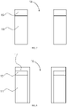
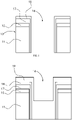
FIG. 7 , thematrix 13 includes asilicon substrate 11 and afirst insulation layer 15. Ahole 16 is formed in thesilicon substrate 11 and thefirst insulation layer 15; thehole 16 penetrates thefirst insulation layer 15 but does not necessarily penetrate thesilicon substrate 11, which is not limited herein. - On the basis of
FIG. 7 , asecond insulation layer 17 is covered on thefirst insulation layer 15, and thesecond insulation layer 17 covers the wall of thehole 16, as shown inFIG. 8 . - On the basis of
FIG. 8 , athird insulation layer 18 is covered on thesecond insulation layer 17, and thethird insulation layer 18 covers an upper surface and side surfaces of thesecond insulation layer 17, as shown inFIG. 9 . - On the basis of
FIG. 9 , a firstinitial connection layer 19 is covered on thethird insulation layer 18; the firstinitial connection layer 19 fills part of thehole 16, and anopening 14 is formed above the firstinitial connection layer 19, as shown inFIG. 10 - On the basis of
FIG. 10 , a secondinitial connection layer 32 is covered on the firstinitial connection layer 19, and the secondinitial connection layer 32 fills theopening 14, as shown inFIG. 11 . - On the basis of
FIG. 11 , a part of the secondinitial connection layer 32 which covers an upper surface of the firstinitial connection layer 19 and is located on an outer side of theopening 14 is removed, and theopening 14 is partially exposed, to form thesecond connection layer 212, as shown inFIG. 12 . - On the basis of
FIG. 12 , a thirdinitial connection layer 33 is covered on the firstinitial connection layer 19, and the thirdinitial connection layer 33 fills theopening 14, as shown inFIG. 13 . - On the basis of
FIG. 13 , the thirdinitial connection layer 33 which covers the upper surface of the firstinitial connection layer 19 and is located on the outer side of theopening 14, and a part of the firstinitial connection layer 19 which is located on thethird insulation layer 18 are removed, to form thefirst connection layer 211 and thethird connection layer 213, as shown inFIG. 14 . That is, the semiconductor structure shown inFIG. 1 can be finally formed. - In an embodiment, the
first connection layer 211, thesecond connection layer 212, and thethird connection layer 213 are sequentially formed in thematrix 13. In a direction perpendicular to thematrix 13, projection of thefirst connection layer 211, projection of thesecond connection layer 212, and projection of thethird connection layer 213 coincide with each other. That is, the structure shown inFIG. 3 andFIG. 4 is formed. - Specifically, on the basis of
FIG. 10 , part of the firstinitial connection layer 19 is removed, that is, an area above thehole 16 is exposed, to form thefirst connection layer 211, as shown inFIG. 15 . - On the basis of
FIG. 15 , a secondinitial connection layer 32 is covered on thethird insulation layer 18, and the secondinitial connection layer 32 fills thehole 16, as shown inFIG. 16 . - On the basis of
FIG. 16 , the secondinitial connection layer 32 is partially removed, that is, an area above thehole 16 is exposed, to form thesecond connection layer 212, as shown inFIG. 17 . - On the basis of
FIG. 17 , a thirdinitial connection layer 33 is covered on thethird insulation layer 18, and the thirdinitial connection layer 33 fills thehole 16, as shown inFIG. 18 . - On the basis of
FIG. 18 , the thirdinitial connection layer 33 is partially removed, that is, an upper surface of the thirdinitial connection layer 33 is made to be flush with an upper surface of thethird insulation layer 18, to form thethird connection layer 213, as shown inFIG. 19 . That is, the semiconductor structure shown inFIG. 3 can be finally formed. - It should be noted that, the
first insulation layer 15, thesecond insulation layer 17, and thethird insulation layer 18 may include silicon dioxide (SiO2), silicon oxide carbon (SiOC), silicon nitride (SiN), silicon carbon nitride (SiCN), and other related integrated-circuit insulation materials. - It should be noted that, a formation process of the
first insulation layer 15, thesecond insulation layer 17, thethird insulation layer 18, the secondinitial connection layer 32, and the thirdinitial connection layer 33 can be selected from a group consisting of a physical vapor deposition (PVD) process, a chemical vapor deposition (CVD) process, an atomic layer deposition (ALD) process, an in-situ steam generation (ISSG) process, and a spin on dielectric (SOD) process, etc., which is not limited herein. - The formation process of the
opening 14 and thehole 16 includes lithography and etching. After each coating is formed, a chemical mechanical polishing (CMP) process can be performed to ensure the flatness of the coating. The firstinitial connection layer 19 can be formed by a process such as electroplating or sputtering, which is not limited therein. - In an embodiment, the semiconductor structure can be formed by using the foregoing method of manufacturing a semiconductor structure. The method of manufacturing a semiconductor structure can further include forming a second
conductive layer 30, and the like, which is not limited herein. Thesilicon substrate 11 and the various insulation layers described above are all part of thebase 10, that is, thematrix 13 is a part of thebase 10. Thefirst insulation layer 15, thesecond insulation layer 17, and thethird insulation layer 18 are all part of theinsulation layer 12. - A person skilled in the art may easily think of other implementation solutions of the present disclosure after considering the specification and practicing the content disclosed herein. The present disclosure is intended to cover any variations, purposes or applicable changes of the present disclosure. Such variations, purposes or applicable changes follow the general principle of the present disclosure and include common knowledge or conventional technical means in the technical field which is not disclosed in the present disclosure. The specification and implementations are merely considered as illustrative, and the real scope and spirit of the present disclosure are directed by the appended claims.
- It should be noted that, the present disclosure is not limited to the precise structures that have been described above and shown in the accompanying drawings, and can be modified and changed in many ways without departing from the scope of the present disclosure. The scope of the present disclosure is defined by the appended claims.
Claims (20)
- A semiconductor structure, comprising:a base; anda communication portion, the communication portion being located in the base and the communication portion comprising a first connection layer, a second connection layer, and a third connection layer, the second connection layer being located on the first connection layer, and the third connection layer being located on the second connection layer;wherein the first connection layer, the second connection layer, and the third connection layer comprise different conductive materials, thermal expansion coefficients of the second connection layer and the third connection layer are both less than a thermal expansion coefficient of the first connection layer.
- The semiconductor structure according to claim 1, wherein a thermal expansion coefficient of the second connection layer is less than a thermal expansion coefficient of the third connection layer.
- The semiconductor structure according to claim 1 or 2, wherein the second connection layer or the third connection layer comprises graphene, and the first connection layer comprises copper.
- The semiconductor structure according to claim 1 or 2, wherein the second connection layer is located in the first connection layer
- The semiconductor structure according to claim 4, wherein the third connection layer is located in the first connection layer.
- The semiconductor structure according to claim 5, wherein in a direction perpendicular to the base, a projection of the second connection layer coincides with a projection of the third connection layer;
wherein a top of the third connection layer is flush with a top of the first connection layer. - The semiconductor structure according to claim 4, wherein in a direction perpendicular to the base, a projection of the first connection layer coincides with a projection of the third connection layer.
- The semiconductor structure according to claim 4, wherein a bottom of the third connection layer is flush with a top of the second connection layer and a top of the first connection layer.
- The semiconductor structure according to claim 1 or 2, wherein in a direction perpendicular to the base, a projection of the first connection layer, a projection of the second connection layer, and a projection of the third connection layer coincide with each other.
- The semiconductor structure according to claim 1 or 2, wherein the base comprises:a silicon substrate, a bottom of the second connection layer being lower than an upper surface of the silicon substrate; andan insulation layer, the insulation layer covering the upper surface of the silicon substrate and covering an outer surface of the communication portion.
- The semiconductor structure according to claim 10, wherein a functional layer is formed in the silicon substrate, and the bottom of the second connection layer is lower than a lower surface of the functional layer.
- The semiconductor structure according to claim 10, wherein a top of the second connection layer is higher than the upper surface of the silicon substrate
- The semiconductor structure according to claim 10, wherein a portion of the second connection layer entering the silicon substrate has a depth greater than or equal to 1 um.
- The semiconductor structure according to claim 1, wherein the communication portion is a through-silicon via.
- The semiconductor structure according to claim 1, wherein the second connection layer has a diameter of 200 nm to 10 um, and the second connection layer has a depth of 1 um to 20 um.
- A semiconductor structure, comprising:a base; anda communication portion, the communication portion being located in the base and the communication portion comprising a first connection layer, a second connection layer, and a third connection layer, the second connection layer being located on the first connection layer, and the third connection layer being located on the second connection layer;wherein the second connection layer and the third connection layer both comprise graphene, and thermal expansion coefficients of the second connection layer and the third connection layer are both less than a thermal expansion coefficient of the first connection layer.
- A method of manufacturing a semiconductor structure, comprising:providing a matrix; andforming a communication portion on the matrix, the communication portion comprising a first connection layer, a second connection layer, and a third connection layer, the second connection layer being formed on the first connection layer, and the third connection layer being formed on the second connection layer;wherein the first connection layer, the second connection layer, and the third connection layer comprise different conductive materials, thermal expansion coefficients of the second connection layer and the third connection layer are both less than a thermal expansion coefficient of the first connection layer.
- The method of manufacturing the semiconductor structure according to claim 17, wherein the second connection layer or the third connection layer comprises graphene, and the first connection layer comprises copper.
- The method of manufacturing the semiconductor structure according to claim 17 or 18, wherein an opening is formed in the first connection layer, and the second connection layer and the third connection layer are sequentially formed in the opening.
- The method of manufacturing method of the semiconductor structure according to claim 17 or 18, wherein the first connection layer, the second connection layer, and the third connection layer are sequentially formed in the matrix;
wherein in a direction perpendicular to the matrix, a projection of the first connection layer, a projection of the second connection layer, and a projection of the third connection layer coincide with each other.
Applications Claiming Priority (2)
| Application Number | Priority Date | Filing Date | Title |
|---|---|---|---|
| CN202110265111.5A CN115084000A (en) | 2021-03-10 | 2021-03-10 | Semiconductor structure and manufacturing method thereof |
| PCT/CN2021/112594 WO2022188358A1 (en) | 2021-03-10 | 2021-08-13 | Semiconductor structure and manufacturing method for same |
Publications (2)
| Publication Number | Publication Date |
|---|---|
| EP4086945A1 true EP4086945A1 (en) | 2022-11-09 |
| EP4086945A4 EP4086945A4 (en) | 2023-04-05 |
Family
ID=83194019
Family Applications (1)
| Application Number | Title | Priority Date | Filing Date |
|---|---|---|---|
| EP21865335.0A Pending EP4086945A4 (en) | 2021-03-10 | 2021-08-13 | SEMI-CONDUCTOR STRUCTURE AND METHOD OF MANUFACTURING IT |
Country Status (4)
| Country | Link |
|---|---|
| US (1) | US12400935B2 (en) |
| EP (1) | EP4086945A4 (en) |
| JP (1) | JP7387003B2 (en) |
| KR (1) | KR102760498B1 (en) |
Family Cites Families (29)
| Publication number | Priority date | Publication date | Assignee | Title |
|---|---|---|---|---|
| JP2005244031A (en) | 2004-02-27 | 2005-09-08 | Nec Electronics Corp | Semiconductor device and manufacturing method thereof |
| JP5231733B2 (en) * | 2006-11-27 | 2013-07-10 | パナソニック株式会社 | Through-hole wiring structure and method for forming the same |
| JP5656341B2 (en) | 2007-10-29 | 2015-01-21 | ピーエスフォー ルクスコ エスエイアールエルPS4 Luxco S.a.r.l. | Semiconductor device and manufacturing method thereof |
| KR20110050957A (en) * | 2009-11-09 | 2011-05-17 | 삼성전자주식회사 | Through-via contact of semiconductor device and forming method |
| TW201145493A (en) * | 2010-06-01 | 2011-12-16 | Chipmos Technologies Inc | Silicon wafer structure and multi-chip stack structure |
| CN104011848A (en) | 2010-07-30 | 2014-08-27 | 昆山智拓达电子科技有限公司 | A through-silicon via interconnection structure and manufacturing method thereof |
| US9059262B2 (en) | 2011-02-24 | 2015-06-16 | Taiwan Semiconductor Manufacturing Company, Ltd. | Integrated circuits including conductive structures through a substrate and methods of making the same |
| US9006102B2 (en) | 2011-04-21 | 2015-04-14 | Globalfoundries Singapore Pte Ltd | Hybrid TSV and method for forming the same |
| JP2013247139A (en) | 2012-05-23 | 2013-12-09 | Ps4 Luxco S A R L | Semiconductor device and method of manufacturing the same |
| CN103545275B (en) | 2012-07-12 | 2016-02-17 | 中芯国际集成电路制造(上海)有限公司 | Silicon through hole encapsulating structure and formation method |
| US20140145332A1 (en) | 2012-11-26 | 2014-05-29 | Globalfoundries Inc. | Methods of forming graphene liners and/or cap layers on copper-based conductive structures |
| JP6175931B2 (en) | 2013-06-21 | 2017-08-09 | 富士通株式会社 | Conductive structure and manufacturing method thereof, electronic device and manufacturing method thereof |
| US9620480B1 (en) | 2013-06-28 | 2017-04-11 | STATS ChipPAC Pte. Ltd | Integrated circuit packaging system with unplated leadframe and method of manufacture thereof |
| US9147642B2 (en) * | 2013-10-31 | 2015-09-29 | Nanya Technology Corporation | Integrated circuit device |
| US10847442B2 (en) | 2014-02-24 | 2020-11-24 | Micron Technology, Inc. | Interconnect assemblies with through-silicon vias and stress-relief features |
| US9466569B2 (en) * | 2014-11-12 | 2016-10-11 | Freescale Semiconductor, Inc. | Though-substrate vias (TSVs) and method therefor |
| CN105810649B (en) | 2014-12-29 | 2018-11-27 | 格科微电子(上海)有限公司 | Semiconductor device bonding structure and its bonding method |
| US20160192488A1 (en) | 2014-12-30 | 2016-06-30 | Samsung Electro-Mechanics Co., Ltd. | Circuit board, multilayered substrate having the circuit board and method of manufacturing the circuit board |
| JP2016139648A (en) | 2015-01-26 | 2016-08-04 | 株式会社東芝 | Semiconductor device and manufacturing method thereof |
| US20170309549A1 (en) | 2016-04-21 | 2017-10-26 | Texas Instruments Incorporated | Sintered Metal Flip Chip Joints |
| CN107068611A (en) * | 2016-12-23 | 2017-08-18 | 苏州能讯高能半导体有限公司 | The manufacture method of semiconductor chip, semiconductor crystal wafer and semiconductor crystal wafer |
| JP7079075B2 (en) | 2017-07-28 | 2022-06-01 | セイコーインスツル株式会社 | package |
| CN107731667B (en) | 2017-08-28 | 2019-06-14 | 长江存储科技有限责任公司 | Hybrid bonding method with metal connection and hybrid bonding structure |
| JP6988345B2 (en) | 2017-10-02 | 2022-01-05 | 株式会社デンソー | Semiconductor device |
| CN108933101A (en) | 2018-07-13 | 2018-12-04 | 河南汇纳科技有限公司 | A kind of TSV structure for eliminating thermal stress |
| US10707151B2 (en) * | 2018-11-20 | 2020-07-07 | Nanya Technology Corporation | Through silicon via structure and method for manufacturing the same |
| JP2020109452A (en) | 2019-01-07 | 2020-07-16 | 株式会社ジャパンディスプレイ | Display device and manufacturing method for display device |
| CN109950221A (en) | 2019-04-15 | 2019-06-28 | 德淮半导体有限公司 | Semiconductor device and its manufacturing method |
| CN112151503B (en) | 2020-08-17 | 2022-10-25 | 复旦大学 | Graphene/copper composite interconnection structure and manufacturing method thereof |
-
2021
- 2021-08-13 KR KR1020227021434A patent/KR102760498B1/en active Active
- 2021-08-13 JP JP2022538973A patent/JP7387003B2/en active Active
- 2021-08-13 EP EP21865335.0A patent/EP4086945A4/en active Pending
-
2022
- 2022-01-24 US US17/648,722 patent/US12400935B2/en active Active
Also Published As
| Publication number | Publication date |
|---|---|
| US20220293493A1 (en) | 2022-09-15 |
| JP7387003B2 (en) | 2023-11-27 |
| JP2023521264A (en) | 2023-05-24 |
| KR102760498B1 (en) | 2025-02-03 |
| EP4086945A4 (en) | 2023-04-05 |
| KR20220127812A (en) | 2022-09-20 |
| US12400935B2 (en) | 2025-08-26 |
Similar Documents
| Publication | Publication Date | Title |
|---|---|---|
| US8492818B2 (en) | High capacitance trench capacitor | |
| US20230013420A1 (en) | Semiconductor structure and fabrication method thereof | |
| TWI793742B (en) | Method for forming semiconductor device with air gap between bit line and capacitor contact | |
| US11107810B2 (en) | Fin field effect transistor (FinFET) device structure and method for forming the same | |
| US11271000B2 (en) | Method for fabricating semiconductor device | |
| CN107799534A (en) | Semiconductor device structure with autoregistration capacitor devices | |
| TW202234577A (en) | Semiconductor device with air gap between two conductive features and method for prepraring | |
| US11665886B2 (en) | Method for fabricating semiconductor device with carbon liner over gate structure | |
| CN115424990A (en) | Semiconductor structure and preparation method thereof | |
| US12400935B2 (en) | Semiconductor structure and manufacturing method thereof | |
| JP7462064B2 (en) | Semiconductor structure and method of manufacturing the same - Patents.com | |
| US20240371856A1 (en) | Semiconductor device structure with fuse and resistor and method for preparing the same | |
| US20220293456A1 (en) | Semiconductor structure and method for manufacturing semiconductor structure | |
| WO2022188358A1 (en) | Semiconductor structure and manufacturing method for same | |
| WO2022188346A1 (en) | Semiconductor structure and method for manufacturing semiconductor structure | |
| WO2011148444A1 (en) | Semiconductor device and method for manufacturing same | |
| RU2808203C1 (en) | Semiconductor structure and method of its manufacture | |
| TWI879243B (en) | Semiconductor structure and method of manufacturing the same | |
| CN115835622B (en) | Semiconductor structure and manufacturing method thereof | |
| TWI905788B (en) | Semiconductor device having air gap between bit line stricture and capacitor contact | |
| CN119300362B (en) | Novel 3D-structured memory and its fabrication method | |
| TW202516692A (en) | Semiconductor device with thermal conductive bonding structure and method of forming the same | |
| CN121728775A (en) | Semiconductor structure and manufacturing method thereof | |
| CN115332059A (en) | Semiconductor device and method for manufacturing the same | |
| CN120475714A (en) | Semiconductor structure and method for manufacturing the same |
Legal Events
| Date | Code | Title | Description |
|---|---|---|---|
| STAA | Information on the status of an ep patent application or granted ep patent |
Free format text: STATUS: UNKNOWN |
|
| STAA | Information on the status of an ep patent application or granted ep patent |
Free format text: STATUS: THE INTERNATIONAL PUBLICATION HAS BEEN MADE |
|
| PUAI | Public reference made under article 153(3) epc to a published international application that has entered the european phase |
Free format text: ORIGINAL CODE: 0009012 |
|
| STAA | Information on the status of an ep patent application or granted ep patent |
Free format text: STATUS: REQUEST FOR EXAMINATION WAS MADE |
|
| 17P | Request for examination filed |
Effective date: 20220316 |
|
| AK | Designated contracting states |
Kind code of ref document: A1 Designated state(s): AL AT BE BG CH CY CZ DE DK EE ES FI FR GB GR HR HU IE IS IT LI LT LU LV MC MK MT NL NO PL PT RO RS SE SI SK SM TR |
|
| A4 | Supplementary search report drawn up and despatched |
Effective date: 20230306 |
|
| RIC1 | Information provided on ipc code assigned before grant |
Ipc: H01L 23/48 20060101ALI20230228BHEP Ipc: H01L 21/768 20060101AFI20230228BHEP |
|
| DAV | Request for validation of the european patent (deleted) | ||
| DAX | Request for extension of the european patent (deleted) | ||
| STAA | Information on the status of an ep patent application or granted ep patent |
Free format text: STATUS: EXAMINATION IS IN PROGRESS |
|
| 17Q | First examination report despatched |
Effective date: 20250718 |