EP4086816A1 - Neural network circuit and neural network system - Google Patents
Neural network circuit and neural network system Download PDFInfo
- Publication number
- EP4086816A1 EP4086816A1 EP21750118.8A EP21750118A EP4086816A1 EP 4086816 A1 EP4086816 A1 EP 4086816A1 EP 21750118 A EP21750118 A EP 21750118A EP 4086816 A1 EP4086816 A1 EP 4086816A1
- Authority
- EP
- European Patent Office
- Prior art keywords
- neural network
- circuit
- computation
- output
- control signal
- Prior art date
- Legal status (The legal status is an assumption and is not a legal conclusion. Google has not performed a legal analysis and makes no representation as to the accuracy of the status listed.)
- Pending
Links
- 238000013528 artificial neural network Methods 0.000 title claims abstract description 224
- 238000005070 sampling Methods 0.000 claims abstract description 20
- 230000008859 change Effects 0.000 claims description 6
- 238000004590 computer program Methods 0.000 claims description 4
- 239000002699 waste material Substances 0.000 abstract description 5
- 239000010410 layer Substances 0.000 description 43
- 230000006870 function Effects 0.000 description 20
- 238000010586 diagram Methods 0.000 description 18
- 238000000034 method Methods 0.000 description 15
- 210000004027 cell Anatomy 0.000 description 13
- 238000012545 processing Methods 0.000 description 11
- 239000003990 capacitor Substances 0.000 description 10
- 230000010354 integration Effects 0.000 description 7
- 230000008569 process Effects 0.000 description 7
- 230000008878 coupling Effects 0.000 description 5
- 238000010168 coupling process Methods 0.000 description 5
- 238000005859 coupling reaction Methods 0.000 description 5
- 239000011159 matrix material Substances 0.000 description 5
- 238000006243 chemical reaction Methods 0.000 description 4
- 238000011176 pooling Methods 0.000 description 4
- 238000013527 convolutional neural network Methods 0.000 description 3
- 230000007274 generation of a signal involved in cell-cell signaling Effects 0.000 description 3
- 210000004205 output neuron Anatomy 0.000 description 3
- 230000002093 peripheral effect Effects 0.000 description 3
- 238000013473 artificial intelligence Methods 0.000 description 2
- 230000007423 decrease Effects 0.000 description 2
- 210000000352 storage cell Anatomy 0.000 description 2
- 238000009825 accumulation Methods 0.000 description 1
- 230000008901 benefit Effects 0.000 description 1
- 238000013529 biological neural network Methods 0.000 description 1
- 230000005540 biological transmission Effects 0.000 description 1
- 210000004556 brain Anatomy 0.000 description 1
- 210000003169 central nervous system Anatomy 0.000 description 1
- 230000001149 cognitive effect Effects 0.000 description 1
- 238000004891 communication Methods 0.000 description 1
- 238000005094 computer simulation Methods 0.000 description 1
- 230000001934 delay Effects 0.000 description 1
- 238000013461 design Methods 0.000 description 1
- 230000006872 improvement Effects 0.000 description 1
- 238000010801 machine learning Methods 0.000 description 1
- 238000013507 mapping Methods 0.000 description 1
- 238000013178 mathematical model Methods 0.000 description 1
- 230000004048 modification Effects 0.000 description 1
- 238000012986 modification Methods 0.000 description 1
- 210000002569 neuron Anatomy 0.000 description 1
- 239000002356 single layer Substances 0.000 description 1
- 230000000946 synaptic effect Effects 0.000 description 1
Images


Classifications
-
- G—PHYSICS
- G06—COMPUTING; CALCULATING OR COUNTING
- G06N—COMPUTING ARRANGEMENTS BASED ON SPECIFIC COMPUTATIONAL MODELS
- G06N3/00—Computing arrangements based on biological models
- G06N3/02—Neural networks
- G06N3/06—Physical realisation, i.e. hardware implementation of neural networks, neurons or parts of neurons
- G06N3/063—Physical realisation, i.e. hardware implementation of neural networks, neurons or parts of neurons using electronic means
- G06N3/065—Analogue means
-
- G—PHYSICS
- G06—COMPUTING; CALCULATING OR COUNTING
- G06N—COMPUTING ARRANGEMENTS BASED ON SPECIFIC COMPUTATIONAL MODELS
- G06N3/00—Computing arrangements based on biological models
- G06N3/02—Neural networks
- G06N3/06—Physical realisation, i.e. hardware implementation of neural networks, neurons or parts of neurons
- G06N3/063—Physical realisation, i.e. hardware implementation of neural networks, neurons or parts of neurons using electronic means
-
- G—PHYSICS
- G06—COMPUTING; CALCULATING OR COUNTING
- G06N—COMPUTING ARRANGEMENTS BASED ON SPECIFIC COMPUTATIONAL MODELS
- G06N3/00—Computing arrangements based on biological models
- G06N3/02—Neural networks
- G06N3/04—Architecture, e.g. interconnection topology
- G06N3/045—Combinations of networks
-
- G—PHYSICS
- G06—COMPUTING; CALCULATING OR COUNTING
- G06N—COMPUTING ARRANGEMENTS BASED ON SPECIFIC COMPUTATIONAL MODELS
- G06N3/00—Computing arrangements based on biological models
- G06N3/02—Neural networks
- G06N3/04—Architecture, e.g. interconnection topology
- G06N3/048—Activation functions
-
- G—PHYSICS
- G06—COMPUTING; CALCULATING OR COUNTING
- G06N—COMPUTING ARRANGEMENTS BASED ON SPECIFIC COMPUTATIONAL MODELS
- G06N3/00—Computing arrangements based on biological models
- G06N3/02—Neural networks
- G06N3/04—Architecture, e.g. interconnection topology
- G06N3/0495—Quantised networks; Sparse networks; Compressed networks
-
- G—PHYSICS
- G11—INFORMATION STORAGE
- G11C—STATIC STORES
- G11C11/00—Digital stores characterised by the use of particular electric or magnetic storage elements; Storage elements therefor
- G11C11/54—Digital stores characterised by the use of particular electric or magnetic storage elements; Storage elements therefor using elements simulating biological cells, e.g. neuron
-
- G—PHYSICS
- G11—INFORMATION STORAGE
- G11C—STATIC STORES
- G11C13/00—Digital stores characterised by the use of storage elements not covered by groups G11C11/00, G11C23/00, or G11C25/00
- G11C13/0002—Digital stores characterised by the use of storage elements not covered by groups G11C11/00, G11C23/00, or G11C25/00 using resistive RAM [RRAM] elements
-
- G—PHYSICS
- G06—COMPUTING; CALCULATING OR COUNTING
- G06N—COMPUTING ARRANGEMENTS BASED ON SPECIFIC COMPUTATIONAL MODELS
- G06N3/00—Computing arrangements based on biological models
- G06N3/02—Neural networks
- G06N3/04—Architecture, e.g. interconnection topology
- G06N3/0464—Convolutional networks [CNN, ConvNet]
-
- G—PHYSICS
- G11—INFORMATION STORAGE
- G11C—STATIC STORES
- G11C2213/00—Indexing scheme relating to G11C13/00 for features not covered by this group
- G11C2213/70—Resistive array aspects
- G11C2213/77—Array wherein the memory element being directly connected to the bit lines and word lines without any access device being used
-
- H—ELECTRICITY
- H03—ELECTRONIC CIRCUITRY
- H03M—CODING; DECODING; CODE CONVERSION IN GENERAL
- H03M1/00—Analogue/digital conversion; Digital/analogue conversion
- H03M1/12—Analogue/digital converters
- H03M1/1205—Multiplexed conversion systems
- H03M1/123—Simultaneous, i.e. using one converter per channel but with common control or reference circuits for multiple converters
-
- H—ELECTRICITY
- H03—ELECTRONIC CIRCUITRY
- H03M—CODING; DECODING; CODE CONVERSION IN GENERAL
- H03M1/00—Analogue/digital conversion; Digital/analogue conversion
- H03M1/12—Analogue/digital converters
- H03M1/50—Analogue/digital converters with intermediate conversion to time interval
- H03M1/56—Input signal compared with linear ramp
-
- H—ELECTRICITY
- H03—ELECTRONIC CIRCUITRY
- H03M—CODING; DECODING; CODE CONVERSION IN GENERAL
- H03M1/00—Analogue/digital conversion; Digital/analogue conversion
- H03M1/66—Digital/analogue converters
- H03M1/68—Digital/analogue converters with conversions of different sensitivity, i.e. one conversion relating to the more significant digital bits and another conversion to the less significant bits
-
- H—ELECTRICITY
- H03—ELECTRONIC CIRCUITRY
- H03M—CODING; DECODING; CODE CONVERSION IN GENERAL
- H03M1/00—Analogue/digital conversion; Digital/analogue conversion
- H03M1/66—Digital/analogue converters
- H03M1/74—Simultaneous conversion
- H03M1/80—Simultaneous conversion using weighted impedances
- H03M1/802—Simultaneous conversion using weighted impedances using capacitors, e.g. neuron-mos transistors, charge coupled devices
-
- Y—GENERAL TAGGING OF NEW TECHNOLOGICAL DEVELOPMENTS; GENERAL TAGGING OF CROSS-SECTIONAL TECHNOLOGIES SPANNING OVER SEVERAL SECTIONS OF THE IPC; TECHNICAL SUBJECTS COVERED BY FORMER USPC CROSS-REFERENCE ART COLLECTIONS [XRACs] AND DIGESTS
- Y02—TECHNOLOGIES OR APPLICATIONS FOR MITIGATION OR ADAPTATION AGAINST CLIMATE CHANGE
- Y02D—CLIMATE CHANGE MITIGATION TECHNOLOGIES IN INFORMATION AND COMMUNICATION TECHNOLOGIES [ICT], I.E. INFORMATION AND COMMUNICATION TECHNOLOGIES AIMING AT THE REDUCTION OF THEIR OWN ENERGY USE
- Y02D10/00—Energy efficient computing, e.g. low power processors, power management or thermal management
Definitions
- This application relates to the field of artificial intelligence, and in particular, to a neural network circuit and a neural network system.
- Neural network is a tool to realize artificial intelligence and has the characteristics of high computation volume and intensive memory access when processing input data.
- a method for improving processing efficiency of a neural network is to deploy the neural network by using an in-memory computing architecture. By utilizing the feature that a weight remains unchanged when the neural network computes, the weight is written into a computing storage medium in advance. Weight storage and computation are completed simultaneously, reducing consumption of time and energy by data exchange and computation.
- a neural network computation array is a core module of a neural network circuit.
- a neural network computation array may also be referred to as a computation array.
- a multiply - add computation array generally constructed by a non-volatile storage medium includes several rows and columns. The row may also be referred to as a word line (wordline), and the column may also be referred to as a bit line (bitline).
- a crosspoint of a row and a column is a computation storage cell of a computation array, or a cell (cell) for short.
- ADC analog to digital converter
- the precision of an existing neural network may be lower than a required computation precision, or a relatively higher precision may lead to a waste of power consumption.
- This application provides a neural network circuit and a neural network system. Output precision of the neural network circuit can be adjusted based on computation precision of the neural network, so that the output precision of the neural network circuit adapts to a change of the computation precision of the neural network.
- a neural network circuit including: a first neural network computation array, a first sample-and-hold circuit, a reference voltage generation circuit, a first comparator circuit, and a first output circuit.
- the first neural network computation array includes a first group of computation units and the first group of computation units is configured to perform neural network computation on a first part of input data based on a weight, to obtain a first output current.
- the first sample-and-hold circuit is connected to the first group of computation units, and is configured to generate a first analog voltage based on the first output current.
- the reference voltage generation circuit is configured to generate a reference voltage based on a first control signal, the first control signal is determined based on first computation precision, and the first control signal changes with a change of the first computation precision.
- the first comparator circuit is connected to the first sample-and-hold circuit and the reference voltage generation circuit, and is configured to output a first level signal based on the first analog voltage and the reference voltage.
- the first output circuit is configured to sample the first level signal based on a second control signal, and output a first computation result, where the first computation result is a computation result that meets the first computation precision, and the second control signal is used to control a frequency at which the first output circuit samples the first level signal.
- the first computation precision changes accordingly. For example, a larger first output current requires higher precision of the neural network.
- the neural network circuit may improve precision of the first computation result by increasing the sampling frequency of the first output circuit and extending duration of the first level signal, so as to meet the precision requirement of the neural network. This avoids lower precision that fails to meet required computation precision or a waste of power consumption caused by high precision.
- the neural network circuit further includes a parameter adjustment circuit, configured to generate the first control signal and the second control signal based on the first computation precision.
- the first level signal when the first analog voltage is higher than the reference voltage, the first level signal is a high level signal; and when the first analog voltage is lower than the reference voltage, the first level signal is a low level signal.
- the first neural network computation array further includes a second group of computation units, and the second group of computation units is configured to perform neural network computation on a second part of data based on a weight, to obtain a second output current.
- the neural network circuit further includes a second sample-and-hold circuit, a second comparator circuit, and a second output circuit.
- the second sample-and-hold circuit is connected to the second group of computation units, and is configured to generate a second analog voltage based on the second output current.
- the second comparator circuit is connected to the second sample-and-hold circuit and the reference voltage generation circuit, and is configured to output a second level signal based on the second analog voltage and the reference voltage.
- the second output circuit is configured to sample the second level signal based on the second control signal, and output a second computation result, where the second computation result is a computation result that meets the first computation precision, and the second control signal is used to control a frequency at which the second output circuit samples the second level signal.
- Multiple groups of computation units may share one parameter adjustment circuit and one reference voltage generation circuit, thereby reducing quantity of components and power consumption.
- the neural network circuit further includes a second neural network computation array.
- the first output circuit is connected to an input end of the second neural network computation array, and the second neural network computation array is configured to compute, based on a weight, data input into the second neural network computation array.
- the data input into the second neural network computation array includes the first computation result, and the first computation result is a pulse signal.
- the first computation result is a pulse signal
- the first computation result can be used by another computation array without performing conversion processing, and no component such as a register or a shift accumulator is required, thereby reducing quantity of components and power consumption required for conversion processing.
- the reference voltage is a ramp voltage.
- an initial voltage of the reference voltage is controlled by the first control signal.
- the first level signal (COMP_OUT) output by the first comparator circuit maintains a ReLU functional relationship with an input current (Current_IN) of the first sample-and-hold circuit, giving the first comparator circuit a function of the ReLU function. Therefore, in this embodiment, the function of the ReLU function can be implemented without an additional component.
- the parameter adjustment circuit is further configured to generate a third control signal based on the first computation precision.
- the third control signal is used to control a reference current of an operational amplifier OPA in the first sample-and-hold circuit, to control precision of the first analog voltage and power consumption of the first sample-and-hold circuit.
- the OPA can operate under the control signal generated by the parameter adjustment circuit.
- the control signal is used to control a reference current of the OPA, so as to reduce power consumption on a premise that a precision requirement of an output voltage of the first sample-and-hold circuit is met.
- the parameter adjustment circuit is further configured to control a sampling start time point of the first output circuit.
- this embodiment can implement a function of a normal ReLU function or a function of a biased ReLU function without additional components.
- a neural network system including a neural network circuit according to any implementation of the first aspect, a memory, and a processor.
- the memory is configured to store input data.
- the processor is configured to read the input data from the memory, and input the input data into the neural network circuit, so that the neural network circuit performs neural network computation on the input data.
- the first computation precision changes accordingly. For example, a larger first output current requires higher precision of the neural network.
- the neural network circuit may improve precision of the first computation result by increasing the sampling frequency of the first output circuit and extending duration of the first level signal, so as to meet the precision requirement of the neural network. This avoidslower precision that fails to meet required computation precision or a waste of power consumption caused by high precision.
- the memory is further configured to store a computer program.
- the processor is further configured to invoke the computer program from the memory to program a neural network computation array in the neural network circuit, and the programming is used to configure a weight of the neural network.
- An artificial neural network (artificial neural network, ANN), referred to as a neural network (neural network, NN) or a neural-like network for short, is a mathematical model or a computational model that mimics a structure and function of a biological neural network (a central nervous system of an animal, especially a brain) in the field of machine learning and cognitive science, and is used for function estimation or approximation.
- the artificial neural network may include neural networks such as a convolutional neural network (convolutional neural network, CNN), a deep neural network (deep neural network, DNN), a multilayer perceptron (multilayer perceptron, MLP), or the like.
- FIG. 1 is a schematic diagram of a structure of a neural network system according to an embodiment of the present invention.
- a neural network system 100 may include a host 105 and a neural network circuit 110.
- a neural network circuit 110 is connected to the host 105 by using a host interface.
- the host interface may include a standard host interface and a network interface (network interface).
- the host interface may include a peripheral component interconnect express (peripheral component interconnect express, PCIE) interface.
- PCIE peripheral component interconnect express
- the neural network circuit 110 may be connected to the host 105 by using a PCIE bus 106. Therefore, data may be input to the neural network circuit 110 by using the PCIE bus 106, and the data after processing performed by the neural network circuit 110 is received by using the PCIE bus 106.
- the host 105 may monitor a working status of the neural network circuit 110 by using the host interface.
- the host 105 may include a processor 1052 and a memory 1054. It should be noted that, in addition to the components shown in FIG. 1 , the host 105 may further include other components such as a communication interface and a magnetic disk used as an external memory. This is not limited herein.
- the processor (processor) 1052 is a computing core and control core (control unit) of the host 105.
- the processor 1052 may include a plurality of processor cores (core).
- the processor 1052 may be an integrated circuit with an ultra-large scale.
- An operating system and another software program are installed in the processor 1052, so that the processor 1052 can access the memory 1054, a cache, a magnetic disk, and a peripheral device (for example, the neural network circuit in FIG. 1 ).
- the core of the processor 1052 may be, for example, a central processing unit (central processing unit, CPU) or another application-specific integrated circuit (application specific integrated circuit, ASIC).
- the memory 1054 is a main memory of the host 105.
- the memory 1054 is connected to the processor 1052 by using a double data rate (double data rate, DDR) bus.
- the memory 1054 is usually configured to store various software running in the operating system, input data and output data, information exchanged with an external memory, and the like. To improve an access rate of the processor 1052, the memory 1054 needs to have an advantage of a high access rate.
- a dynamic random access memory dynamic random access memory, DRAM
- the processor 1052 can access the memory 1054 at a high rate by using a memory controller (not shown in FIG. 1 ), and perform a read operation and a write operation on any storage cell in the memory 1054.
- the neural network circuit 110 is a chip array including a plurality of neural network chips (chip).
- the neural network circuit 110 includes a plurality of neural network chips (chip, C) 115 that perform data processing and a plurality of routers (router, R) 120.
- the neural network chip 115 in this application is referred to as a chip 115 for short in this embodiment of the present invention.
- the plurality of chips 115 are connected to each other through the routers 120.
- one chip 115 may be connected to one or more routers 120.
- the plurality of routers 120 may form one or more network topologies. Data transmission may be performed between the chips 115 by using the plurality of network topologies.
- the neural network system 100 shown in FIG. 1 is an example of the neural network system provided in this application, and should not be construed as a limitation on the protection scope of this application.
- the neural network system applicable to this application may further include more circuits or fewer circuits.
- the neural network chips may be directly connected without a router.
- a neural network may include a plurality of neural network layers.
- the neural network layer is a logical layer concept, and one neural network layer means that one neural network operation needs to be performed. Computing of each neural network layer is implemented by a computing node.
- the neural network layer may include a convolutional layer, a pooling layer, and the like.
- the neural network may include n neural network layers (which may also be referred to as n layers of a neural network).
- n is an integer greater than or equal to 2.
- FIG. 2 is a schematic diagram of some neural network layers in the neural network.
- a neural network 200 may include a first layer 202, a second layer 204, a third layer 206, a fourth layer 208, a fifth layer 210 to an n th layer 212.
- the first layer 202 may perform a convolution operation
- the second layer 204 may perform a pooling operation on output data of the first layer 202
- the third layer 206 may perform a convolution operation on output data of the second layer 204
- the fourth layer 208 may perform a convolution operation on an output result of the third layer 206
- the fifth layer 210 may perform a summation operation on the output data of the second layer 204 and output data of the fourth layer 208, and the like.
- FIG. 2 shows only a simple example and a description of neural network layers in a neural network, and a specific operation of each neural network layer is not limited.
- the fourth layer 208 may perform a pooling operation
- the fifth layer 210 may perform another neural network operation such as a convolution operation or a pooling operation.
- a computation result of the i th layer is temporarily stored in a preset cache.
- a computation unit needs to load the computation result of the i th layer and a weight of the (i + 1) th layer from the preset cache to perform computation.
- the i th layer is any layer in the neural network.
- the neural network circuit for example a neural network chip C in FIG. 1
- the neural network circuit uses a computation array constructed by a non-volatile storage medium. Therefore, a weight may be configured on a cell of the computation array before computation.
- the computation result can be directly sent to a next layer for pipeline computation. Therefore, each neural network layer only needs to cache very little data. For example, each neural network layer needs to cache input data enough only for one time of window computing.
- a neural network circuit containing a computation array is shown in Figure 3 .
- a neural network circuit 300 includes:
- a circuit in the neural network circuit 300 other than the input circuit 301, the drive circuit 302, and the first computation array 303 may be referred to as a neuron core circuit.
- circuit module division is an example, and is merely a logical function division. In actual implementation, another division manner may be used.
- circuits and the connection relationship between the circuits are examples rather than limitations. A person skilled in the art can reconstruct the neural network circuit 300 without creative efforts.
- one circuit may be integrated into another circuit, and the connection relationship changes accordingly.
- the drive circuit 302 may be integrated into the input circuit 301, and the first computation array 303 is connected to the input circuit 301.
- the first comparator circuit 307 may be integrated into the first sample-and-hold circuit 305, and the first output circuit 308 and the reference voltage generation circuit 306 are connected to the first sample-and-hold circuit 305.
- some circuits may be removed.
- the parameter adjustment circuit 304 may be removed, and another circuit in the neural network circuit 300 may operate based on a control signal input externally or information preset internally.
- first and second are used to indicate different individuals of a same type.
- first comparator circuit 307 and the second comparator circuit described below indicate two different comparator circuits. Other than that, there is no other limitation.
- the neural network circuit 300 may be a submodule of the neural network circuit 110 in the neural network system 100 shown in FIG. 1 (That is, the neural network circuit 300 is a neural network chip C in FIG. 1 ).
- the neural network system 100 may first program the first computation array 303, that is, complete mapping from a weight of the neural network to a conductance value.
- the input circuit 301 may send the input data to the drive circuit 302 in time division, and 1 bit (bit) information is sent in each clock cycle. For example, if the input data is 10, the input circuit 301 may send 1 in 10 consecutive clock cycles, and then send 0 after that in all clock cycles after the 10 consecutive clock cycles. This output method is called rate-coding (rate-coding).
- the drive circuit 302 may convert the 1s and 0s into voltage signals and load the voltage signals onto the first computation array 303.
- the first sample-and-hold circuit 305 accumulates currents in time domain output by the first group of computation units in the first computation array 303 for time until the input data is all input.
- the first computation array 303 may operate simultaneously with the drive circuit 302. The following describes, with reference to FIG. 4 , a working process in which the first computation array 303 performs an operation based on the neural network weight and the input data.
- the weight is usually used to indicate importance of input data to output data.
- the weight is usually presented by using a matrix.
- the matrix of j rows and k columns shown in Table 1 may be a weight of a neural network layer, and each element in the matrix represents a weight value.
- the weights may be configured on the first computation array in advance.
- an element in a matrix is configured in a cell of a computation array, and one element is configured for each unit, so that, by using the computation array, a multiply-add operation can be performed on the input data and a matrix representing a weight.
- One computation array may include a plurality of cells, such as G 1,1 , G 2,1 , and the like. Cells are located at row-column intersections. If a computation array includes 1000 rows and 1000 columns, a quantity of cells in the computation array is one million.
- the weights shown in Table 1 may be input into the computation array through bitlines (an input port 402 in FIG. 4 ) of the computation array shown in FIG. 4 , so that each weight value in the weights is configured into a corresponding cell. For example, the weight value W 0, 0 in Table 1 is configured to G 1, 1 in FIG.
- each weight value corresponds to one cell, and each weight value is stored in the cell in a form of conductance.
- input data is input into the computation array through wordlines (an input port 404 shown in FIG. 4 ) of the computation array.
- the input data can be represented by voltages (such as V 1 , V 2 , V 3 , and V 4 ), so that a dot multiplication operation is performed between the input data and the weight value stored in the cell, and the obtained computation result is output in a form of a current from an output end of each column (an output port 406 shown in FIG. 4 ) of the computation array.
- I GV.
- the computation array in which the weights are stored may also be referred to as a synaptic array.
- the computation array shown in FIG. 4 is a 1T1R array, and 1T1R means that each cell has one transmit end and one receive end.
- a computation array applicable to this application may alternatively be a 1T2R array, a 2T2R array, or another type of array.
- the first comparator circuit 307 and the reference voltage generation circuit 306 start to work. At the same time, the first output circuit 308 is also operating.
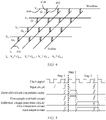
- An operation time sequence of each circuit in the neural network circuit 300 is shown in FIG. 5 .
- the precision requirement of the neural network changes with a change of a magnitude of the current output by the first group of computation units.
- a larger first output current requires higher precision of the neural network.
- the parameter adjustment circuit 304 may improve precision of the first computation result by increasing the sampling frequency of the first output circuit 308 and extending duration of the first level signal, to meet the precision requirement of the neural network.
- the parameter adjustment circuit 304 may generate a control signal X1 and a control signal X2 based on the computation precision B.
- the control signal X1 controls the reference voltage generation circuit 306 to generate a reference voltage.
- the first comparator circuit 307 After comparing the first analog voltage with the reference voltage, the first comparator circuit 307 generates a voltage signal with longer duration. In this way, the first output circuit 308 can sample more information.
- the control signal X2 may control the first output circuit 308 to increase the sampling frequency, and sample more information per unit time.
- the parameter adjustment circuit 304 may generate a control signal X3 and a control signal X4 based on the computation precision C.
- the control signal X3 controls the reference voltage generation circuit 306 to generate a reference voltage.
- the first comparator circuit 307 After comparing the first analog voltage with the reference voltage, the first comparator circuit 307 generates a voltage signal with shorter duration. In this way, power consumption of the neural network circuit 300 can be reduced on the premise that sufficient information is sampled by the first output circuit 308.
- the control signal X4 controls the first output circuit 308 to reduce the sampling frequency. This reduces power consumption of the neural network circuit 300 while sufficient information is sampled per unit time.
- the neural network circuit 300 can adapt to a change in computation precision of the neural network. This avoids that a computation precision requirement cannot be met in a case of low precision, and that a waste of power consumption is caused in a case of high precision
- FIG. 6 is a schematic diagram of an optional structure of the neural network circuit 300.
- an input circuit 601 in addition to sending input data to a first computation array, an input circuit 601 further sends, to a parameter adjustment circuit 604, information used for parameter control, for example, output range information, initial voltage information, and precision information.
- the parameter adjustment circuit 604 includes various functional circuits, such as an output range adjustment circuit, an initial voltage control circuit, and a precision adjustment circuit.
- the output range information is, for example, a quantity of rows enabled by the first computation array and an algorithm requirement.
- the output range adjustment circuit After obtaining the output range information from an output circuit, the output range adjustment circuit generates a control signal K that controls the switched capacitor.
- the control signal K is used to control a switch group (K i0 , K i1 , and K i2 ) in a first sample-and-hold circuit, and switches in the switch group are connected to integration capacitors.
- the first sample-and-hold circuit 605 may include an operational amplifier (operational amplifier, OPA) and an integration capacitor.
- the integration capacitors are C i0 , C i1 , and C i2 as in FIG. 6 .
- S&H_OUT is an output voltage (a first analog voltage) of the first sample-and-hold circuit 605
- Current_IN is an input current of the first sample-and-hold circuit 605
- A is a linear coefficient.
- the integration capacitor controlled by the switch group may scale a ratio of an input current to an output voltage of the first sample-and-hold circuit 605.
- the linear coefficient A is a scaling multiple of the input current and the output voltage of the first sample-and-hold circuit 605.
- the OPA can operate under a control signal L generated by a precision adjustment circuit.
- the control signal L is used to control a reference current of the OPA, and power consumption is reduced on a premise that a precision requirement of an output voltage of the first sample-and-hold circuit 605 is met. After the reference current decreases, a current of an amplifier of the OPA decreases under mirroring of the current mirror, reducing power consumption of the first sample-and-hold circuit 605.
- RST_integ is a reset switch
- EN_integ is an enable switch
- V CLP is a clamp voltage
- the precision information described above is used by the parameter adjustment circuit 604 to generate a control signal, for example, the control signal L generated by an OPA current controller and a clock control signal (CLK_ramp and CLK_out) generated after a frequency divider (frequency divider) modulates a clock signal (CLK) of the neural network system.
- a control signal for example, the control signal L generated by an OPA current controller and a clock control signal (CLK_ramp and CLK_out) generated after a frequency divider (frequency divider) modulates a clock signal (CLK) of the neural network system.
- CLK_ramp and CLK_out clock control signal
- CLK clock signal
- the clock control signal K is used to control a ramp voltage generated by a ramp voltage generation circuit 606, and the ramp voltage generation circuit 606 is an example of the reference voltage generation circuit 306 described above.
- the ramp voltage output by the ramp voltage generation circuit 606 and the first analog voltage output by the first sample-and-hold circuit 605 are used by the first comparator circuit 607 to generate the first level signal.
- An operating principle of the first comparator circuit 607 is as follows: When the first analog voltage is higher than the ramp voltage, the first level signal is a high level signal.
- the first level signal is a low level signal.
- FIG. 7 to FIG. 9 are several examples in which the first comparator circuit generates a first level signal based on a ramp voltage and a first analog voltage.
- V represents a voltage
- t represents a time
- S&H_OUT represents the first analog voltage output by the first sample-and-hold circuit 605
- Ramp_OUT represents the ramp voltage output by the ramp voltage generation circuit 606
- COMP_OUT represents the first level signal output by the first comparator circuit 607
- Neuron_OUT represents the first computation result obtained after the first output circuit 608 samples the first level signal.
- values of the first analog voltages are the same.
- a slope of Ramp_OUT in FIG. 7 is less than a slope of Ramp_OUT in FIG. 8 .
- duration of COMP_OUT in FIG. 7 is longer than duration of COMP_OUT in FIG. 8 .
- information amount of Neuron_OUT in FIG. 7 is more than information amount of Neuron_OUT in FIG. 8 .
- the slope of the ramp voltage is controlled by the clock control signal CLK_ramp, and it can be seen that the parameter adjustment circuit 604 can control the output precision of the neural network circuit shown in FIG. 6 .
- the longer duration of the high level signal the higher power consumption. Therefore, the parameter adjustment circuit 604 can further control the power consumption of the neural network circuit shown in FIG. 6 by controlling the slope of the ramp voltage.
- the slope of Ramp_OUT in FIG. 7 is less than a slope of Ramp_OUT in FIG. 9 . Therefore, the duration of COMP_OUT in FIG. 7 is equal to duration of COMP_OUT in FIG. 9 .
- the frequency in FIG. 7 at which the first output circuit 608 samples COMP_OUT is higher than the frequency in FIG. 9 at which the first output circuit 608 samples COMP_OUT. Therefore, information amount of Neuron_OUT in FIG. 7 is more than information amount of Neuron_OUT in FIG. 9 .
- the sampling frequency of the first output circuit 608 is controlled by the clock control signal CLK_out, and it can be seen that the parameter adjustment circuit 604 can control the output precision of the neural network circuit shown in FIG. 6 . In addition, the higher sampling frequency, the higher power consumption. Therefore, the parameter adjustment circuit 604 can further control the power consumption of the neural network circuit shown in FIG. 6 by controlling the sampling frequency.
- the parameter adjustment circuit 604 may control output precision and power consumption of the neural network circuit shown in FIG. 6 by using both CLK_ramp and CLK_out, or may control the output precision and power consumption of the neural network circuit by using either CLK_ramp or CLK_out.
- the power consumption can be reduced on the premise that the output precision of the neural network circuit is satisfied.
- the parameter adjustment circuit 604 may further control sampling start time point of the first output circuit 608.
- an initial voltage control circuit acquires initial voltage information from the input circuit 601
- the initial voltage control circuit outputs a voltage signal and applies it to a DAC of the ramp voltage generation circuit 606 to control an initial voltage of the ramp voltage.
- the DAC is a segmented switched-capacitor DAC and is configured to generate a ramp voltage.
- C 0 to C 9 are segmented switched-capacitors in the DAC, and C 1 to C 9 may be connected to the ground (GND) under switches control.
- the ramp voltage generation circuit 606 further includes a counter.
- a bit width of the counter is, for example, 8 bits, and 256 types of control signals may be output under control of CLK_ramp.
- S1 to S8 are used to control switches corresponding to C 1 to C 9 . to adjust the slope of the ramp voltage.
- the first comparator circuit 607 can output COMP_OUT in FIG. 10 , that is, COMP_OUT maintains a ReLU functional relationship with an input current Current_IN of the first sample-and-hold circuit 605.
- the first comparator circuit 605 has a function of a ReLU function.
- the first output circuit 608 delays the sampling start time point under the control of the parameter adjustment circuit 604 a relationship between Neuron_OUT and Current_IN generated by the first output circuit 608 is shown in FIG. 11 , and presents a forward biased ReLU functional relationship.
- the delay means that sampling starts after the control signal of the parameter adjustment circuit 604 is received, and sampling is not performed on the first level signal before the control signal.
- the first output circuit 608 may further advance the sampling start time point under the control of the parameter adjustment circuit 604, so that Neuron_OUT and Current_IN present a reverse biased ReLU functional relationship.
- the neural network circuit shown in FIG. 6 further includes a first output circuit 608.
- the first output circuit 608 can output two results: one is a data signal Y1 output by a counter, and the other is a pulse signal Y0.
- Y0 may be generated based on Y1.
- the bit width of the counter is 8 bits, there may be eight precision choices for Y1, as ⁇ 0:7> in FIG. 6 .
- the input signal of the first computation array is usually a pulse signal.
- the first output circuit 608 may output Y0.
- the result output by the first output circuit 608 can be used by another computation array without conversion processing. Therefore, components such as a register and a shift accumulator, and components such as a register and a shift accumulator are not needed. This reduces a quantity of components and power consumption required for conversion processing.
- a and FIG. 13B For example, as shown in FIG. 13 , when a first output circuit 1308 outputs Y0, Y0 may be directly loaded onto a second computation array 13114 by a drive circuit 1313 of a second neural network circuit. Therefore, an input circuit 1312 of the second neural network circuit in FIG. 13A and FIG. 13B is an optional module.
- the first output circuit 608 may output Y1.
- the foregoing describes in detail a process in which the first computation array outputs one output current (that is, the first output current).
- the first computation array may output a plurality of output currents
- a neural network circuit provided in this application is shown in FIG. 12 .
- a first computation array 1203 includes a plurality of groups of computation units, for example, a first group of computation units and a second group of computation units.
- the first group of computation units and the second group of computation units compute different input data based on weights, and output different output currents.
- the second group of computation units outputs a second output current to a second sample-and-hold circuit 1209.
- the second sample-and-hold circuit 1209 converts the second output current into a second analog voltage under control of the control signal L and the control signal K.
- the second comparator circuit 1210 outputs a second level signal based on the second analog voltage and a reference voltage (for example, a ramp voltage).
- the second output circuit 1211 samples the second level signal to generate a second computation result.
- different groups of computation units in the first computation array 1203 use different sample-and-hold circuits, comparator circuits, and output circuits, and a parameter adjustment circuit 1204 and a reference voltage generation circuit 1206 are shared by all groups of computation units. This reduces a quantity of components and power consumption.
- the neural network circuit shown in FIG. 12 is a circuit applicable to a single-layer neural network.
- another circuit may be connected to the neural network circuit shown in FIG. 12 , to meet a requirement of a multilayer neural network.
- FIG. 13A and FIG. 13B are a schematic diagram of a neural network circuit applicable to a multilayer neural network.
- a first neural network circuit is, for example, the circuit shown in FIG. 12 .
- An input bit width of the first neural network circuit is M
- a scale of the first computation array is M ⁇ N
- there are N output neurons that is, N output circuits.
- An input bit width of the second neural network circuit is N
- a scale of the second computation array is N ⁇ K
- K output neurons that is, K output circuits.
- the output neuron of the second neural network circuit may further be connected to another neural network circuit.
- FIG. 14 Anoperation time sequence of the circuit in FIG. 13A and FIG. 13B is shown in FIG. 14 .
- the input circuit, the drive circuit, the computation array, and the sample-and-hold circuit of the second neural network circuit also work.
- An optional workflow is as follows:
- the neural network system outputs the final computation result.
- precision of the first neural network circuit and the second neural network circuit may be represented by N1 and N2.
- the first neural network circuit may output 2 N1 pulses, where each pulse is used as an input of the second neural network circuit.
- the second neural network circuit may output 2 N2 pulses. Therefore, output precision of the second neural network circuit is (N1 + N2) bits.
- precision of ramp voltages of the first neural network circuit and the second neural network circuit is 8 bits.
- both N1 and N2 are 1-8 bits
- an output precision range of the second neural network circuit is 2-16 bits.
- the foregoing describes in detail an example of the neural network circuit and the neural network system that are provided in this application.
- the neural network circuit and the neural network system include a corresponding hardware structure and/or software module for performing each function.
- a person skilled in the art may be easily aware that this application can be implemented in a form of hardware or a combination of hardware and computer software with reference to the disclosed embodiments of this specification. Whether a specific function is performed by hardware or hardware driven by computer software depends on particular applications and design constraints of the technical solutions. A person skilled in the art may use different methods to implement the described functions for each particular application, but it should not be considered that the implementation goes beyond the scope of this application.
- the disclosed system, apparatus and method may be implemented in other manners. For example, some features of the method embodiments described above may be ignored or not performed.
- the described apparatus embodiments are merely examples.
- the unit division is merely logical function division and may be other division in actual implementation.
- a plurality of units or components may be combined or integrated into another system.
- coupling between the units or coupling between the components may be direct coupling or indirect coupling, and the coupling may include an electrical connection, a mechanical connection, or another form of connection.
- sequence indexes of the foregoing processes do not mean execution sequences in the various embodiments of this application.
- the execution sequences of the processes need to be determined based on functions and internal logic of the processes, and do not need to be construed as any limitation on the implementation processes of the embodiments of this application.
Landscapes
- Engineering & Computer Science (AREA)
- Physics & Mathematics (AREA)
- Theoretical Computer Science (AREA)
- Health & Medical Sciences (AREA)
- Life Sciences & Earth Sciences (AREA)
- Biomedical Technology (AREA)
- Biophysics (AREA)
- General Health & Medical Sciences (AREA)
- Molecular Biology (AREA)
- General Physics & Mathematics (AREA)
- Computational Linguistics (AREA)
- Evolutionary Computation (AREA)
- Computing Systems (AREA)
- General Engineering & Computer Science (AREA)
- Data Mining & Analysis (AREA)
- Mathematical Physics (AREA)
- Software Systems (AREA)
- Artificial Intelligence (AREA)
- Neurology (AREA)
- Computer Hardware Design (AREA)
- Feedback Control In General (AREA)
- Combined Controls Of Internal Combustion Engines (AREA)
Abstract
Description
- This application claims priority to
Chinese Patent Application No. 202010083080.7, filed with China National Intellectual Property Administration on February 7, 2020 - This application relates to the field of artificial intelligence, and in particular, to a neural network circuit and a neural network system.
- Neural network is a tool to realize artificial intelligence and has the characteristics of high computation volume and intensive memory access when processing input data. A method for improving processing efficiency of a neural network is to deploy the neural network by using an in-memory computing architecture. By utilizing the feature that a weight remains unchanged when the neural network computes, the weight is written into a computing storage medium in advance. Weight storage and computation are completed simultaneously, reducing consumption of time and energy by data exchange and computation.
- In the in-memory computing architecture, a neural network computation array is a core module of a neural network circuit. A neural network computation array may also be referred to as a computation array. A multiply - add computation array generally constructed by a non-volatile storage medium includes several rows and columns. The row may also be referred to as a word line (wordline), and the column may also be referred to as a bit line (bitline). A crosspoint of a row and a column is a computation storage cell of a computation array, or a cell (cell) for short. When the neural network computes, a weight is stored in a cell in advance in the form of conductance. After being processed by a digital-to-analog converter (digital to analog converter, DAC), input data enters the computation array in the form of voltage. Subsequently, the voltage forms an electric current after corresponding conductance and the currents converge on a same column. A sum of obtained currents may be used to represent an accumulation result of a product of the input data and the weight. The current further needs to be restored to a digital signal by an analog-to-digital converter (analog to digital converter, ADC).
- and Fixed precisions of the DAC and the ADC cannot adapt to a changed computation precision of the neural network. Therefore, the precision of an existing neural network may be lower than a required computation precision, or a relatively higher precision may lead to a waste of power consumption.
- This application provides a neural network circuit and a neural network system. Output precision of the neural network circuit can be adjusted based on computation precision of the neural network, so that the output precision of the neural network circuit adapts to a change of the computation precision of the neural network.
- According to a first aspect, a neural network circuit is provided, including: a first neural network computation array, a first sample-and-hold circuit, a reference voltage generation circuit, a first comparator circuit, and a first output circuit. The first neural network computation array includes a first group of computation units and the first group of computation units is configured to perform neural network computation on a first part of input data based on a weight, to obtain a first output current. The first sample-and-hold circuit is connected to the first group of computation units, and is configured to generate a first analog voltage based on the first output current. The reference voltage generation circuit is configured to generate a reference voltage based on a first control signal, the first control signal is determined based on first computation precision, and the first control signal changes with a change of the first computation precision. The first comparator circuit is connected to the first sample-and-hold circuit and the reference voltage generation circuit, and is configured to output a first level signal based on the first analog voltage and the reference voltage. The first output circuit is configured to sample the first level signal based on a second control signal, and output a first computation result, where the first computation result is a computation result that meets the first computation precision, and the second control signal is used to control a frequency at which the first output circuit samples the first level signal.
- When a value of the first output current changes, the first computation precision changes accordingly. For example, a larger first output current requires higher precision of the neural network. The neural network circuit may improve precision of the first computation result by increasing the sampling frequency of the first output circuit and extending duration of the first level signal, so as to meet the precision requirement of the neural network. This avoids lower precision that fails to meet required computation precision or a waste of power consumption caused by high precision.
- Optionally, the neural network circuit further includes a parameter adjustment circuit, configured to generate the first control signal and the second control signal based on the first computation precision.
- Optionally, when the first analog voltage is higher than the reference voltage, the first level signal is a high level signal; and when the first analog voltage is lower than the reference voltage, the first level signal is a low level signal.
- Optionally, the first neural network computation array further includes a second group of computation units, and the second group of computation units is configured to perform neural network computation on a second part of data based on a weight, to obtain a second output current. The neural network circuit further includes a second sample-and-hold circuit, a second comparator circuit, and a second output circuit. The second sample-and-hold circuit is connected to the second group of computation units, and is configured to generate a second analog voltage based on the second output current. The second comparator circuit is connected to the second sample-and-hold circuit and the reference voltage generation circuit, and is configured to output a second level signal based on the second analog voltage and the reference voltage. The second output circuit is configured to sample the second level signal based on the second control signal, and output a second computation result, where the second computation result is a computation result that meets the first computation precision, and the second control signal is used to control a frequency at which the second output circuit samples the second level signal.
- Multiple groups of computation units may share one parameter adjustment circuit and one reference voltage generation circuit, thereby reducing quantity of components and power consumption.
- Optionally, the neural network circuit further includes a second neural network computation array. The first output circuit is connected to an input end of the second neural network computation array, and the second neural network computation array is configured to compute, based on a weight, data input into the second neural network computation array. The data input into the second neural network computation array includes the first computation result, and the first computation result is a pulse signal.
- When the first computation result is a pulse signal, the first computation result can be used by another computation array without performing conversion processing, and no component such as a register or a shift accumulator is required, thereby reducing quantity of components and power consumption required for conversion processing.
- Optionally, the reference voltage is a ramp voltage.
- Optionally, an initial voltage of the reference voltage is controlled by the first control signal.
- When the initial voltage of the ramp voltage equals to an initial voltage of the first analog voltage, the first level signal (COMP_OUT) output by the first comparator circuit maintains a ReLU functional relationship with an input current (Current_IN) of the first sample-and-hold circuit, giving the first comparator circuit a function of the ReLU function. Therefore, in this embodiment, the function of the ReLU function can be implemented without an additional component.
- Optionally, the parameter adjustment circuit is further configured to generate a third control signal based on the first computation precision. The third control signal is used to control a reference current of an operational amplifier OPA in the first sample-and-hold circuit, to control precision of the first analog voltage and power consumption of the first sample-and-hold circuit.
- The OPA can operate under the control signal generated by the parameter adjustment circuit. The control signal is used to control a reference current of the OPA, so as to reduce power consumption on a premise that a precision requirement of an output voltage of the first sample-and-hold circuit is met.
- Optionally, the parameter adjustment circuit is further configured to control a sampling start time point of the first output circuit.
- When the sampling start time point of the first output circuit does not shift, an output result of the first output circuit and an output current of the first sample-and-hold circuit present a normal ReLU functional relationship; and when the sampling start time point of the first output circuit shifts, an output result of the first output circuit and an output current of the first sample-and-hold circuit present a bias ReLU functional relationship. Therefore, this embodiment can implement a function of a normal ReLU function or a function of a biased ReLU function without additional components.
- According to a second aspect, a neural network system is provided, including a neural network circuit according to any implementation of the first aspect, a memory, and a processor. The memory is configured to store input data. The processor is configured to read the input data from the memory, and input the input data into the neural network circuit, so that the neural network circuit performs neural network computation on the input data.
- When a value of the first output current changes, the first computation precision changes accordingly. For example, a larger first output current requires higher precision of the neural network. The neural network circuit may improve precision of the first computation result by increasing the sampling frequency of the first output circuit and extending duration of the first level signal, so as to meet the precision requirement of the neural network. This avoidslower precision that fails to meet required computation precision or a waste of power consumption caused by high precision.
- Optionally, the memory is further configured to store a computer program. The processor is further configured to invoke the computer program from the memory to program a neural network computation array in the neural network circuit, and the programming is used to configure a weight of the neural network.
-
-
FIG. 1 is a schematic diagram of a structure of a neural network system according to this application; -
FIG. 2 is a schematic diagram of some neural network layers in a neural network according to this application; -
FIG. 3 is a schematic diagram of a structure of a neural network circuit according to this application; -
FIG. 4 is a schematic diagram of a structure of a computation array according to this application; -
FIG. 5 is a schematic diagram of an operation time sequence of a neural network circuit according to this application; -
FIG. 6 is a schematic diagram of a structure of another neural network circuit according to this application; -
FIG. 7 is a schematic diagram of a level signal generation method according to this application; -
FIG. 8 is a schematic diagram of another level signal generation method according to this application; -
FIG. 9 is a schematic diagram of yet another level signal generation method according to this application; -
FIG. 10 is a schematic diagram of an output result of a comparator circuit according to this application; -
FIG. 11 is a schematic diagram of an output result of an output circuit according to this application; -
FIG. 12 is a schematic diagram of a structure of a neural network circuit with multiple groups of computation units according to this application; -
FIG. 13A andFIG. 13B are a schematic diagram of a structure of a neural network circuit applicable to a multilayer neural network according to this application; and -
FIG. 14 is a schematic diagram of an operation time sequence of another neural network circuit according to this application. - To facilitate understanding of the technical solutions in this application, concepts in this application are first briefly described.
- An artificial neural network (artificial neural network, ANN), referred to as a neural network (neural network, NN) or a neural-like network for short, is a mathematical model or a computational model that mimics a structure and function of a biological neural network (a central nervous system of an animal, especially a brain) in the field of machine learning and cognitive science, and is used for function estimation or approximation. The artificial neural network may include neural networks such as a convolutional neural network (convolutional neural network, CNN), a deep neural network (deep neural network, DNN), a multilayer perceptron (multilayer perceptron, MLP), or the like.
FIG. 1 is a schematic diagram of a structure of a neural network system according to an embodiment of the present invention. As shown inFIG. 1 , aneural network system 100 may include ahost 105 and aneural network circuit 110. Aneural network circuit 110 is connected to thehost 105 by using a host interface. The host interface may include a standard host interface and a network interface (network interface). For example, the host interface may include a peripheral component interconnect express (peripheral component interconnect express, PCIE) interface. As shown inFIG. 1 , theneural network circuit 110 may be connected to thehost 105 by using aPCIE bus 106. Therefore, data may be input to theneural network circuit 110 by using thePCIE bus 106, and the data after processing performed by theneural network circuit 110 is received by using thePCIE bus 106. In addition, thehost 105 may monitor a working status of theneural network circuit 110 by using the host interface. - The
host 105 may include aprocessor 1052 and amemory 1054. It should be noted that, in addition to the components shown inFIG. 1 , thehost 105 may further include other components such as a communication interface and a magnetic disk used as an external memory. This is not limited herein. - The processor (processor) 1052 is a computing core and control core (control unit) of the
host 105. Theprocessor 1052 may include a plurality of processor cores (core). Theprocessor 1052 may be an integrated circuit with an ultra-large scale. An operating system and another software program are installed in theprocessor 1052, so that theprocessor 1052 can access thememory 1054, a cache, a magnetic disk, and a peripheral device (for example, the neural network circuit inFIG. 1 ). It may be understood that, in an embodiment of the present invention, the core of theprocessor 1052 may be, for example, a central processing unit (central processing unit, CPU) or another application-specific integrated circuit (application specific integrated circuit, ASIC). - The
memory 1054 is a main memory of thehost 105. Thememory 1054 is connected to theprocessor 1052 by using a double data rate (double data rate, DDR) bus. Thememory 1054 is usually configured to store various software running in the operating system, input data and output data, information exchanged with an external memory, and the like. To improve an access rate of theprocessor 1052, thememory 1054 needs to have an advantage of a high access rate. In a conventional computer system architecture, a dynamic random access memory (dynamic random access memory, DRAM) is usually used as thememory 1054. Theprocessor 1052 can access thememory 1054 at a high rate by using a memory controller (not shown inFIG. 1 ), and perform a read operation and a write operation on any storage cell in thememory 1054. - The
neural network circuit 110 is a chip array including a plurality of neural network chips (chip). For example, as shown inFIG. 1 , theneural network circuit 110 includes a plurality of neural network chips (chip, C) 115 that perform data processing and a plurality of routers (router, R) 120. For ease of description, theneural network chip 115 in this application is referred to as achip 115 for short in this embodiment of the present invention. The plurality ofchips 115 are connected to each other through therouters 120. For example, onechip 115 may be connected to one ormore routers 120. The plurality ofrouters 120 may form one or more network topologies. Data transmission may be performed between thechips 115 by using the plurality of network topologies. - The
neural network system 100 shown inFIG. 1 is an example of the neural network system provided in this application, and should not be construed as a limitation on the protection scope of this application. The neural network system applicable to this application may further include more circuits or fewer circuits. For example, the neural network chips may be directly connected without a router. - A person skilled in the art may know that a neural network may include a plurality of neural network layers. In this embodiment of the present invention, the neural network layer is a logical layer concept, and one neural network layer means that one neural network operation needs to be performed. Computing of each neural network layer is implemented by a computing node. The neural network layer may include a convolutional layer, a pooling layer, and the like. As shown in
FIG. 2 , the neural network may include n neural network layers (which may also be referred to as n layers of a neural network). Herein, n is an integer greater than or equal to 2. -
FIG. 2 is a schematic diagram of some neural network layers in the neural network. As shown inFIG. 2 , aneural network 200 may include afirst layer 202, asecond layer 204, athird layer 206, afourth layer 208, afifth layer 210 to an nth layer 212. Thefirst layer 202 may perform a convolution operation, thesecond layer 204 may perform a pooling operation on output data of thefirst layer 202, thethird layer 206 may perform a convolution operation on output data of thesecond layer 204, thefourth layer 208 may perform a convolution operation on an output result of thethird layer 206, thefifth layer 210 may perform a summation operation on the output data of thesecond layer 204 and output data of thefourth layer 208, and the like. It may be understood thatFIG. 2 shows only a simple example and a description of neural network layers in a neural network, and a specific operation of each neural network layer is not limited. For example, thefourth layer 208 may perform a pooling operation, and thefifth layer 210 may perform another neural network operation such as a convolution operation or a pooling operation. - In some neural networks, after computation of an ith layer in the neural network is completed, a computation result of the ith layer is temporarily stored in a preset cache. When computation of an (i + 1)th layer is performed, a computation unit needs to load the computation result of the ith layer and a weight of the (i + 1)th layer from the preset cache to perform computation. The ith layer is any layer in the neural network. In this embodiment of the present invention, the neural network circuit (for example a neural network chip C in
FIG. 1 ) of the neural network system uses a computation array constructed by a non-volatile storage medium. Therefore, a weight may be configured on a cell of the computation array before computation. The computation result can be directly sent to a next layer for pipeline computation. Therefore, each neural network layer only needs to cache very little data. For example, each neural network layer needs to cache input data enough only for one time of window computing. - A neural network circuit containing a computation array is shown in
Figure 3 . Aneural network circuit 300 includes: - An
input circuit 301, configured to store input data of a neural network, and send the input data to adrive circuit 302; - The
drive circuit 302, connected to theinput circuit 301, and configured to convert the input data into a voltage signal that can be applied to afirst computation array 303; - The
first computation array 303, connected to thedrive circuit 302, and configured to generate an output current based on the voltage signal input by thedrive circuit 302 and a pre-stored weight; - A first sample-and-
hold circuit 305, connected to a first group of computation units in thefirst computation array 303, and configured to generate a first analog voltage based on a first output current, where the first group of computation units may belong to one column of computation units, or may belong to a plurality of columns of computation units; - A
parameter adjustment circuit 304, connected to theinput circuit 301 and the first sample-and-hold circuit 305, and configured to adjust a parameter of each circuit in theneural network circuit 300 by using a control signal, for example, generate a first control signal and a second control signal described below; - A reference
voltage generation circuit 306, connected to theparameter adjustment circuit 304, and configured to generate a reference voltage (for example, a ramp voltage) based on the first control signal, where the first control signal is determined based on first computation precision, and the first control signal changes with a change of the first computation precision; - A
first comparator circuit 307, connected to the first sample-and-hold circuit 305 and the referencevoltage generation circuit 306, and configured to output a first level signal based on the first analog voltage and the reference voltage; - A
first output circuit 308, connected to thefirst comparator circuit 307 and theparameter adjustment circuit 304, and configured to sample the first level signal based on a second control signal and output a first computation result, where the first computation result is a computation result that meets the first computation precision, and the second control signal is used to control a frequency at which thefirst output circuit 308 samples the first level signal. - A circuit in the
neural network circuit 300 other than theinput circuit 301, thedrive circuit 302, and thefirst computation array 303 may be referred to as a neuron core circuit. - It should be noted that, in this application, circuit module division is an example, and is merely a logical function division. In actual implementation, another division manner may be used. The foregoing circuits and the connection relationship between the circuits are examples rather than limitations. A person skilled in the art can reconstruct the
neural network circuit 300 without creative efforts. - In some cases, one circuit may be integrated into another circuit, and the connection relationship changes accordingly. For example, the
drive circuit 302 may be integrated into theinput circuit 301, and thefirst computation array 303 is connected to theinput circuit 301. Thefirst comparator circuit 307 may be integrated into the first sample-and-hold circuit 305, and thefirst output circuit 308 and the referencevoltage generation circuit 306 are connected to the first sample-and-hold circuit 305. - In other cases, some circuits may be removed. For example, the
parameter adjustment circuit 304 may be removed, and another circuit in theneural network circuit 300 may operate based on a control signal input externally or information preset internally. - In addition, in this application, words such as "first" and "second" are used to indicate different individuals of a same type. For example, the
first comparator circuit 307 and the second comparator circuit described below indicate two different comparator circuits. Other than that, there is no other limitation. - The
neural network circuit 300 may be a submodule of theneural network circuit 110 in theneural network system 100 shown inFIG. 1 (That is, theneural network circuit 300 is a neural network chip C inFIG. 1 ). When performing neural network computation, theneural network system 100 may first program thefirst computation array 303, that is, complete mapping from a weight of the neural network to a conductance value. - Subsequently, the
input circuit 301 may send the input data to thedrive circuit 302 in time division, and 1 bit (bit) information is sent in each clock cycle. For example, if the input data is 10, theinput circuit 301 may send 1 in 10 consecutive clock cycles, and then send 0 after that in all clock cycles after the 10 consecutive clock cycles. This output method is called rate-coding (rate-coding). - The
drive circuit 302 may convert the 1s and 0s into voltage signals and load the voltage signals onto thefirst computation array 303. At the same time, the first sample-and-hold circuit 305 accumulates currents in time domain output by the first group of computation units in thefirst computation array 303 for time until the input data is all input. - The
first computation array 303 may operate simultaneously with thedrive circuit 302. The following describes, with reference toFIG. 4 , a working process in which thefirst computation array 303 performs an operation based on the neural network weight and the input data. - The weight is usually used to indicate importance of input data to output data. In a neural network, the weight is usually presented by using a matrix. As shown in Table 1, the matrix of j rows and k columns shown in Table 1 may be a weight of a neural network layer, and each element in the matrix represents a weight value.
Table 1 W0,0 w0,1 ∗ ∗ ∗ W0.k-1 w1,0 W1,1 ∗ ∗ ∗ W1,k-1 W2,0 W2,1 ∗ ∗ ∗ W2,k-1 W3,0 W3,1 ∗ ∗ ∗ W3,k-1 ∗ ∗ ∗ ∗ ∗ ∗ ∗ ∗ ∗ ∗ ∗ ∗ ∗ ∗ ∗ ∗ ∗ ∗ Wj-1,0 Wj-1,1 ∗ ∗ ∗ Wj-1,k-1 - In this embodiment, the weights may be configured on the first computation array in advance. For example, an element in a matrix is configured in a cell of a computation array, and one element is configured for each unit, so that, by using the computation array, a multiply-add operation can be performed on the input data and a matrix representing a weight.
- A structure of a computation array is shown in
Figure 4 . One computation array may include a plurality of cells, such as G1,1, G2,1, and the like. Cells are located at row-column intersections. If a computation array includes 1000 rows and 1000 columns, a quantity of cells in the computation array is one million. In this embodiment of the present invention, in a process of configuring a neural network, the weights shown in Table 1 may be input into the computation array through bitlines (aninput port 402 inFIG. 4 ) of the computation array shown inFIG. 4 , so that each weight value in the weights is configured into a corresponding cell. For example, the weight value W0, 0 in Table 1 is configured to G1, 1 inFIG. 4 , and the weight value W1, 0 in Table 1 is configured to G2, 1 inFIG. 4 . Each weight value corresponds to one cell, and each weight value is stored in the cell in a form of conductance. When the neural network computation is performed, input data is input into the computation array through wordlines (aninput port 404 shown inFIG. 4 ) of the computation array. The input data can be represented by voltages (such as V1, V2, V3, and V4), so that a dot multiplication operation is performed between the input data and the weight value stored in the cell, and the obtained computation result is output in a form of a current from an output end of each column (anoutput port 406 shown inFIG. 4 ) of the computation array. - The current value output by each column may be calculated with a formula I = GV. For example, the current value output by the first column is denoted as I1, I1 = V1 ∗ G1, 1 + V2 ∗ G2, 1 + V3 ∗ G3, + V4 ∗ G4, 1
- The computation array in which the weights are stored may also be referred to as a synaptic array. The computation array shown in
FIG. 4 is a 1T1R array, and 1T1R means that each cell has one transmit end and one receive end. Optionally, a computation array applicable to this application may alternatively be a 1T2R array, a 2T2R array, or another type of array. - After the first sample-and-
hold circuit 305 finishes processing the output current of thefirst computation array 303, thefirst comparator circuit 307 and the referencevoltage generation circuit 306 start to work. At the same time, thefirst output circuit 308 is also operating. - An operation time sequence of each circuit in the
neural network circuit 300 is shown inFIG. 5 . - The precision requirement of the neural network changes with a change of a magnitude of the current output by the first group of computation units. A larger first output current requires higher precision of the neural network. The
parameter adjustment circuit 304 may improve precision of the first computation result by increasing the sampling frequency of thefirst output circuit 308 and extending duration of the first level signal, to meet the precision requirement of the neural network. - For example, when the precision requirement of the neural network changes from computation precision A to computation precision B (the computation precision B is higher than the computation precision A), the
parameter adjustment circuit 304 may generate a control signal X1 and a control signal X2 based on the computation precision B. The control signal X1 controls the referencevoltage generation circuit 306 to generate a reference voltage. After comparing the first analog voltage with the reference voltage, thefirst comparator circuit 307 generates a voltage signal with longer duration. In this way, thefirst output circuit 308 can sample more information. The control signal X2 may control thefirst output circuit 308 to increase the sampling frequency, and sample more information per unit time. - For another example, when the precision requirement of the neural network changes from computation precision A to computation precision C (the computation precision C is lower than the computation precision A), the
parameter adjustment circuit 304 may generate a control signal X3 and a control signal X4 based on the computation precision C. The control signal X3 controls the referencevoltage generation circuit 306 to generate a reference voltage. After comparing the first analog voltage with the reference voltage, thefirst comparator circuit 307 generates a voltage signal with shorter duration. In this way, power consumption of theneural network circuit 300 can be reduced on the premise that sufficient information is sampled by thefirst output circuit 308. The control signal X4 controls thefirst output circuit 308 to reduce the sampling frequency. This reduces power consumption of theneural network circuit 300 while sufficient information is sampled per unit time. - Therefore, the
neural network circuit 300 can adapt to a change in computation precision of the neural network. This avoids that a computation precision requirement cannot be met in a case of low precision, and that a waste of power consumption is caused in a case of high precision -
FIG. 6 is a schematic diagram of an optional structure of theneural network circuit 300. - In
FIG. 6 , in addition to sending input data to a first computation array, aninput circuit 601 further sends, to aparameter adjustment circuit 604, information used for parameter control, for example, output range information, initial voltage information, and precision information. Theparameter adjustment circuit 604 includes various functional circuits, such as an output range adjustment circuit, an initial voltage control circuit, and a precision adjustment circuit. - The output range information is, for example, a quantity of rows enabled by the first computation array and an algorithm requirement. After obtaining the output range information from an output circuit, the output range adjustment circuit generates a control signal K that controls the switched capacitor. The control signal K is used to control a switch group (Ki0, Ki1, and Ki2) in a first sample-and-hold circuit, and switches in the switch group are connected to integration capacitors.
- The first sample-and-
hold circuit 605 may include an operational amplifier (operational amplifier, OPA) and an integration capacitor. The integration capacitors are Ci0, Ci1, and Ci2 as inFIG. 6 . The integration capacitor integrates an input current (that is, the first output current of the first computation array), and an output voltage of the integration capacitor is in a linear relationship with the input current, that is, S&H_OUT = A ∗ Current_IN. S&H_OUT is an output voltage (a first analog voltage) of the first sample-and-hold circuit 605, Current_IN is an input current of the first sample-and-hold circuit 605, and A is a linear coefficient. When a switch in the switch group is closed and opened, a size of an integration capacitor of the first sample-and-hold circuit 605 changes. The integration capacitor controlled by the switch group may scale a ratio of an input current to an output voltage of the first sample-and-hold circuit 605. The linear coefficient A is a scaling multiple of the input current and the output voltage of the first sample-and-hold circuit 605. - The OPA can operate under a control signal L generated by a precision adjustment circuit. The control signal L is used to control a reference current of the OPA, and power consumption is reduced on a premise that a precision requirement of an output voltage of the first sample-and-
hold circuit 605 is met. After the reference current decreases, a current of an amplifier of the OPA decreases under mirroring of the current mirror, reducing power consumption of the first sample-and-hold circuit 605. - In
FIG. 6 , RST_integ is a reset switch, EN_integ is an enable switch, and VCLP is a clamp voltage. These three features are all optional implementations. - The precision information described above is used by the
parameter adjustment circuit 604 to generate a control signal, for example, the control signal L generated by an OPA current controller and a clock control signal (CLK_ramp and CLK_out) generated after a frequency divider (frequency divider) modulates a clock signal (CLK) of the neural network system. The OPA current controller and the frequency divider may be referred to as precision adjustment modules. The function of the control signal L has been described above, and the function of the clock control signal is described in detail below. - The clock control signal K is used to control a ramp voltage generated by a ramp
voltage generation circuit 606, and the rampvoltage generation circuit 606 is an example of the referencevoltage generation circuit 306 described above. The ramp voltage output by the rampvoltage generation circuit 606 and the first analog voltage output by the first sample-and-hold circuit 605 are used by thefirst comparator circuit 607 to generate the first level signal. - An operating principle of the
first comparator circuit 607 is as follows:
When the first analog voltage is higher than the ramp voltage, the first level signal is a high level signal. - When the first analog voltage is lower than the ramp voltage, the first level signal is a low level signal.
-
FIG. 7 to FIG. 9 are several examples in which the first comparator circuit generates a first level signal based on a ramp voltage and a first analog voltage. V represents a voltage, t represents a time, S&H_OUT represents the first analog voltage output by the first sample-and-hold circuit 605, Ramp_OUT represents the ramp voltage output by the rampvoltage generation circuit 606, COMP_OUT represents the first level signal output by thefirst comparator circuit 607, and Neuron_OUT represents the first computation result obtained after thefirst output circuit 608 samples the first level signal. InFIG. 7 to FIG. 9 , values of the first analog voltages are the same. - A slope of Ramp_OUT in
FIG. 7 is less than a slope of Ramp_OUT inFIG. 8 . When the S&H_OUTs are the same, duration of COMP_OUT inFIG. 7 is longer than duration of COMP_OUT inFIG. 8 . When frequencies at which thefirst output circuit 608 samples the COMP_OUT are the same, information amount of Neuron_OUT inFIG. 7 is more than information amount of Neuron_OUT inFIG. 8 . The slope of the ramp voltage is controlled by the clock control signal CLK_ramp, and it can be seen that theparameter adjustment circuit 604 can control the output precision of the neural network circuit shown inFIG. 6 . In addition, the longer duration of the high level signal, the higher power consumption. Therefore, theparameter adjustment circuit 604 can further control the power consumption of the neural network circuit shown inFIG. 6 by controlling the slope of the ramp voltage. - The slope of Ramp_OUT in
FIG. 7 is less than a slope of Ramp_OUT inFIG. 9 . Therefore, the duration of COMP_OUT inFIG. 7 is equal to duration of COMP_OUT inFIG. 9 . The frequency inFIG. 7 at which thefirst output circuit 608 samples COMP_OUT is higher than the frequency inFIG. 9 at which thefirst output circuit 608 samples COMP_OUT. Therefore, information amount of Neuron_OUT inFIG. 7 is more than information amount of Neuron_OUT inFIG. 9 . The sampling frequency of thefirst output circuit 608 is controlled by the clock control signal CLK_out, and it can be seen that theparameter adjustment circuit 604 can control the output precision of the neural network circuit shown inFIG. 6 . In addition, the higher sampling frequency, the higher power consumption. Therefore, theparameter adjustment circuit 604 can further control the power consumption of the neural network circuit shown inFIG. 6 by controlling the sampling frequency. - The
parameter adjustment circuit 604 may control output precision and power consumption of the neural network circuit shown inFIG. 6 by using both CLK_ramp and CLK_out, or may control the output precision and power consumption of the neural network circuit by using either CLK_ramp or CLK_out. The power consumption can be reduced on the premise that the output precision of the neural network circuit is satisfied. - Optionally, in addition to controlling the output precision of the neural network circuit, the
parameter adjustment circuit 604 may further control sampling start time point of thefirst output circuit 608. - As shown in
FIG. 6 , after an initial voltage control circuit acquires initial voltage information from theinput circuit 601, the initial voltage control circuit outputs a voltage signal and applies it to a DAC of the rampvoltage generation circuit 606 to control an initial voltage of the ramp voltage. The DAC is a segmented switched-capacitor DAC and is configured to generate a ramp voltage. C0 to C9 are segmented switched-capacitors in the DAC, and C1 to C9 may be connected to the ground (GND) under switches control. The rampvoltage generation circuit 606 further includes a counter. A bit width of the counter is, for example, 8 bits, and 256 types of control signals may be output under control of CLK_ramp. As shown in S1 to S8, S1 to S8 are used to control switches corresponding to C1 to C9. to adjust the slope of the ramp voltage. - When the initial voltage of the ramp voltage equals an initial voltage of the first analog voltage, the
first comparator circuit 607 can output COMP_OUT inFIG. 10 , that is, COMP_OUT maintains a ReLU functional relationship with an input current Current_IN of the first sample-and-hold circuit 605. Thefirst comparator circuit 605 has a function of a ReLU function. - When the
first output circuit 608 delays the sampling start time point under the control of theparameter adjustment circuit 604, a relationship between Neuron_OUT and Current_IN generated by thefirst output circuit 608 is shown inFIG. 11 , and presents a forward biased ReLU functional relationship. The delay means that sampling starts after the control signal of theparameter adjustment circuit 604 is received, and sampling is not performed on the first level signal before the control signal. Optionally, thefirst output circuit 608 may further advance the sampling start time point under the control of theparameter adjustment circuit 604, so that Neuron_OUT and Current_IN present a reverse biased ReLU functional relationship. - The neural network circuit shown in
FIG. 6 further includes afirst output circuit 608. Thefirst output circuit 608 can output two results: one is a data signal Y1 output by a counter, and the other is a pulse signal Y0. Y0 may be generated based on Y1. When the bit width of the counter is 8 bits, there may be eight precision choices for Y1, as <0:7> inFIG. 6 . - The input signal of the first computation array is usually a pulse signal. When a result output by the
first output circuit 608 is used as an input signal of another computation array, thefirst output circuit 608 may output Y0. The result output by thefirst output circuit 608 can be used by another computation array without conversion processing. Therefore, components such as a register and a shift accumulator, and components such as a register and a shift accumulator are not needed. This reduces a quantity of components and power consumption required for conversion processing. A andFIG. 13B For example, as shown inFIG. 13 , when afirst output circuit 1308 outputs Y0, Y0 may be directly loaded onto a second computation array 13114 by adrive circuit 1313 of a second neural network circuit. Therefore, aninput circuit 1312 of the second neural network circuit inFIG. 13A andFIG. 13B is an optional module. - If the result output by the
first output circuit 608 is no longer used as an input signal of another computation array, thefirst output circuit 608 may output Y1. - The foregoing describes in detail a process in which the first computation array outputs one output current (that is, the first output current). When the first computation array may output a plurality of output currents, a neural network circuit provided in this application is shown in
FIG. 12 . - In
FIG. 12 , afirst computation array 1203 includes a plurality of groups of computation units, for example, a first group of computation units and a second group of computation units. The first group of computation units and the second group of computation units compute different input data based on weights, and output different output currents. The second group of computation units outputs a second output current to a second sample-and-hold circuit 1209. The second sample-and-hold circuit 1209 converts the second output current into a second analog voltage under control of the control signal L and the control signal K. Thesecond comparator circuit 1210 outputs a second level signal based on the second analog voltage and a reference voltage (for example, a ramp voltage). Thesecond output circuit 1211 samples the second level signal to generate a second computation result. - In
FIG. 12 , different groups of computation units in thefirst computation array 1203 use different sample-and-hold circuits, comparator circuits, and output circuits, and aparameter adjustment circuit 1204 and a referencevoltage generation circuit 1206 are shared by all groups of computation units. This reduces a quantity of components and power consumption. - The neural network circuit shown in
FIG. 12 is a circuit applicable to a single-layer neural network. Optionally, another circuit may be connected to the neural network circuit shown inFIG. 12 , to meet a requirement of a multilayer neural network. -
FIG. 13A andFIG. 13B are a schematic diagram of a neural network circuit applicable to a multilayer neural network. A first neural network circuit is, for example, the circuit shown inFIG. 12 . An input bit width of the first neural network circuit is M, a scale of the first computation array is M ∗ N, and there are N output neurons (that is, N output circuits). An input bit width of the second neural network circuit is N, a scale of the second computation array is N ∗ K, and there are K output neurons (that is, K output circuits). The output neuron of the second neural network circuit may further be connected to another neural network circuit. - Anoperation time sequence of the circuit in
FIG. 13A andFIG. 13B is shown inFIG. 14 . When the reference voltage generation circuit, the comparator circuit, and the output circuit of the first neural network circuit work, the input circuit, the drive circuit, the computation array, and the sample-and-hold circuit of the second neural network circuit also work. An optional workflow is as follows: - 1-S1: In a first step of the first neural network circuit, an
input circuit 1301 of the first neural network circuit outputs input data in a rate-coding manner, and a required time is determined by data amount and a signal bit width. - 1-S2: In a second step of the first neural network circuit, a
drive circuit 1302, afirst computation array 1303, and each sample-and-hold circuit of the first neural network circuit start to work. Thefirst computation array 1303 performs a multiply-add operation on the input data and weights stored in thefirst computation array 1303. The operation result is output after being processed by each sample-and-hold circuit. - 1-S3: In a third step of the first neural network circuit, a reference
voltage generation circuit 1306, each comparator circuit, and each output circuit start to work, to output a first computation result. - 2-S1: In a first step of the second neural network circuit, the
input circuit 1312 of the second neural network circuit samples the first computation result of the first neural network circuit, and outputs a sampling result. - 2-S2: In a second step of the second neural network circuit, the
drive circuit 1313 of the second neural network converts the sampling result of the previous step into an analog voltage signal and the signal is applied to asecond computation array 1314. Thesecond computation array 1314 performs a multiply-add operation on the input data and weights stored in thesecond computation array 1314. The operation result is output after being processed by each sample-and-hold circuit. 1-S3, 2-S1, and 2-S2 coincide. - 2-S3: In a third step of the second neural network circuit, a reference
voltage generation circuit 1317, each comparator circuit, and each output circuit start to work, to output a second computation result. - Then, the neural network system outputs the final computation result.
- In the circuit shown in
FIG. 13A andFIG. 13B , precision of the first neural network circuit and the second neural network circuit may be represented by N1 and N2. The first neural network circuit mayoutput 2N1 pulses, where each pulse is used as an input of the second neural network circuit. For each input, the second neural network circuit mayoutput 2N2 pulses. Therefore, output precision of the second neural network circuit is (N1 + N2) bits. For example, precision of ramp voltages of the first neural network circuit and the second neural network circuit is 8 bits. In this case, both N1 and N2 are 1-8 bits, and an output precision range of the second neural network circuit is 2-16 bits. - The foregoing describes in detail an example of the neural network circuit and the neural network system that are provided in this application. The neural network circuit and the neural network system include a corresponding hardware structure and/or software module for performing each function. A person skilled in the art may be easily aware that this application can be implemented in a form of hardware or a combination of hardware and computer software with reference to the disclosed embodiments of this specification. Whether a specific function is performed by hardware or hardware driven by computer software depends on particular applications and design constraints of the technical solutions. A person skilled in the art may use different methods to implement the described functions for each particular application, but it should not be considered that the implementation goes beyond the scope of this application.
- In the several embodiments provided in this application, the disclosed system, apparatus and method may be implemented in other manners. For example, some features of the method embodiments described above may be ignored or not performed. The described apparatus embodiments are merely examples. The unit division is merely logical function division and may be other division in actual implementation. A plurality of units or components may be combined or integrated into another system. In addition, coupling between the units or coupling between the components may be direct coupling or indirect coupling, and the coupling may include an electrical connection, a mechanical connection, or another form of connection.
- It needs to be understood that sequence indexes of the foregoing processes do not mean execution sequences in the various embodiments of this application. The execution sequences of the processes need to be determined based on functions and internal logic of the processes, and do not need to be construed as any limitation on the implementation processes of the embodiments of this application.
- In summary, what is described above is merely example embodiments of the technical solutions of this application, but is not intended to limit the protection scope of this application. Any modification, equivalent replacement, or improvement made without departing from the spirit and principle of this application shall fall within the protection scope of this application.
Claims (11)
- A neural network circuit, comprising:a first neural network computation array, comprising a first group of computation units, wherein the first group of computation units is configured to, based on a weight, perform neural network computation on a first part of input data, to obtain a first output current;a first sample-and-hold circuit, connected to the first group of computation units, and configured to generate a first analog voltage based on the first output current;a reference voltage generation circuit, configured to generate a reference voltage based on a first control signal, wherein the first control signal is determined based on a first computation precision, and the first control signal changes with a change of the first computation precision;a first comparator circuit, connected to the first sample-and-hold circuit and the reference voltage generation circuit respectively, and configured to output a first level signal based on the first analog voltage and the reference voltage; anda first output circuit, configured to sample the first level signal based on a second control signal, and output a first computation result, wherein the first computation result is a computation result that meets the first computation precision, and the second control signal is used to control a frequency at which the first output circuit samples the first level signal.
- The neural network circuit according to claim 1, further comprising:
a parameter adjustment circuit, configured to generate the first control signal and the second control signal based on the first computation precision. - The neural network circuit according to claim 1 or 2, whereinwhen the first analog voltage is higher than the reference voltage, the first level signal is a high level signal; andwhen the first analog voltage is lower than the reference voltage, the first level signal is a low level signal.
- The neural network circuit according to any one of claims 1 to 3, whereinthe first neural network computation array further comprises a second group of computation units, wherein the second group of computation units is configured to, based on a weight, perform the neural network computation on a second part of data, to obtain a second output current; andthe neural network circuit further comprising:a second sample-and-hold circuit, connected to the second group of computation units, and configured to generate a second analog voltage based on the second output current;a second comparator circuit, connected to the second sample-and-hold circuit and the reference voltage generation circuit respectively, and configured to output a second level signal based on the second analog voltage and the reference voltage; anda second output circuit, configured to sample the second level signal based on the second control signal, and output a second computation result, wherein the second computation result is a computation result that meets the first computation precision, and the second control signal is used to control a frequency at which the second output circuit samples the second level signal.
- The neural network circuit according to any one of claims 1 to 4, further comprising a second neural network computation array, wherein the first output circuit is connected to an input end of the second neural network computation array, and the second neural network computation array is configured to, based on a weight, compute data input into the second neural network computation array; and the data input into the second neural network computation array comprises the first computation result, and the first computation result is a pulse signal.
- The neural network circuit according to any one of claims 1 to 5, wherein the reference voltage is a ramp voltage.
- The neural network circuit according to claim 6, wherein an initial voltage of the ramp voltage is controlled by the first control signal.
- The neural network circuit according to claim 2, wherein the parameter adjustment circuit is further configured to:
generate, based on the first computation precision, a third control signal, wherein the third control signal is used to control a reference current of an operational amplifier OPA in the first sample-and-hold circuit, to control precision of the first analog voltage and power consumption of the first sample-and-hold circuit. - The neural network circuit according to claim 2, wherein the parameter adjustment circuit is further configured to:
control a sampling start time of the first output circuit. - A neural network system, comprising:the neural network circuit according to any one of claims 1 to 9;a memory, configured to store input data;a processor, configured to read the input data from the memory, and input the input data into the neural network circuit, so that the neural network circuit performs neural network computation on the input data.
- The neural network system according to claim 10, whereinthe memory is further configured to store a computer program; andthe processor is further configured to invoke the computer program from the memory, and program a neural network computation array in the neural network circuit, wherein the programming is used to configure a weight of the neural network.
Applications Claiming Priority (2)
| Application Number | Priority Date | Filing Date | Title |
|---|---|---|---|
| CN202010083080.7A CN113255875A (en) | 2020-02-07 | 2020-02-07 | Neural network circuit and neural network system |
| PCT/CN2021/075635 WO2021155851A1 (en) | 2020-02-07 | 2021-02-05 | Neural network circuit and neural network system |
Publications (2)
| Publication Number | Publication Date |
|---|---|
| EP4086816A1 true EP4086816A1 (en) | 2022-11-09 |
| EP4086816A4 EP4086816A4 (en) | 2023-04-26 |
Family
ID=77200786
Family Applications (1)
| Application Number | Title | Priority Date | Filing Date |
|---|---|---|---|
| EP21750118.8A Pending EP4086816A4 (en) | 2020-02-07 | 2021-02-05 | Neural network circuit and neural network system |
Country Status (4)
| Country | Link |
|---|---|
| US (1) | US20220374694A1 (en) |
| EP (1) | EP4086816A4 (en) |
| CN (1) | CN113255875A (en) |
| WO (1) | WO2021155851A1 (en) |
Families Citing this family (3)
| Publication number | Priority date | Publication date | Assignee | Title |
|---|---|---|---|---|
| CN116362314A (en) * | 2021-12-24 | 2023-06-30 | 华为技术有限公司 | Integrated storage and calculation device and calculation method |
| CN115294745B (en) * | 2022-05-23 | 2023-09-29 | 电子科技大学 | Lithium battery thermal runaway layered early warning method based on neural network and data difference |
| CN116579392A (en) * | 2023-02-21 | 2023-08-11 | 鹏城实验室 | Neural network training operation system and method based on conductance adjustable device |
Family Cites Families (5)
| Publication number | Priority date | Publication date | Assignee | Title |
|---|---|---|---|---|
| CN105701541A (en) * | 2016-01-13 | 2016-06-22 | 哈尔滨工业大学深圳研究生院 | Circuit structure based on memristor pulse nerve network |
| JP6703265B2 (en) * | 2016-06-27 | 2020-06-03 | 富士通株式会社 | Neural network device and method for controlling neural network device |
| CN107612546B (en) * | 2017-08-29 | 2020-10-23 | 电子科技大学 | Phase-locked loop circuit based on neural network |
| CN111630527A (en) * | 2017-11-14 | 2020-09-04 | 技术研发基金会有限公司 | Analog-to-digital converter using memory in neural network |
| JP6569755B1 (en) * | 2018-03-06 | 2019-09-04 | Tdk株式会社 | Neural network device, signal generation method and program |
-
2020
- 2020-02-07 CN CN202010083080.7A patent/CN113255875A/en active Pending
-
2021
- 2021-02-05 WO PCT/CN2021/075635 patent/WO2021155851A1/en unknown
- 2021-02-05 EP EP21750118.8A patent/EP4086816A4/en active Pending
-
2022
- 2022-08-05 US US17/882,360 patent/US20220374694A1/en active Pending
Also Published As
| Publication number | Publication date |
|---|---|
| CN113255875A (en) | 2021-08-13 |
| US20220374694A1 (en) | 2022-11-24 |
| WO2021155851A1 (en) | 2021-08-12 |
| EP4086816A4 (en) | 2023-04-26 |
Similar Documents
| Publication | Publication Date | Title |
|---|---|---|
| US10860682B2 (en) | Binary, ternary and bit serial compute-in-memory circuits | |
| EP3389051B1 (en) | Memory device and data-processing method based on multi-layer rram crossbar array | |
| EP4086816A1 (en) | Neural network circuit and neural network system | |
| US20200356848A1 (en) | Computing circuitry | |
| CN114400031B (en) | Complement mapping RRAM (resistive random access memory) storage and calculation integrated chip and electronic equipment | |
| US20230161627A1 (en) | High-energy-efficiency binary neural network accelerator applicable to artificial intelligence internet of things | |
| WO2021222821A1 (en) | Voltage offset for compute-in-memory architecture | |
| WO2021178585A1 (en) | Compute-in-memory dynamic random access memory | |
| TWI803889B (en) | Computing device and computing method | |
| KR102318819B1 (en) | In-memory device for operation of multi-bit Weight | |
| CN118072788A (en) | Integrated circuit, chip and electronic equipment for memory and calculation | |
| US20220262426A1 (en) | Memory System Capable of Performing a Bit Partitioning Process and an Internal Computation Process | |
| US20230253032A1 (en) | In-memory computation device and in-memory computation method to perform multiplication operation in memory cell array according to bit orders | |
| US20220223197A1 (en) | Memory unit with asymmetric group-modulated input scheme and current-to-voltage signal stacking scheme for non-volatile computing-in-memory applications and computing method thereof | |
| US20240176587A1 (en) | Multi-bit analog multiplication and accumulation circuit system | |
| US5708598A (en) | System and method for reading multiple voltage level memories | |
| WO2024174354A1 (en) | Operating system and method for training of neural network based on conductance-adjustable device | |
| US11621723B2 (en) | Input-shaping method and input-shaping unit for group-modulated input scheme in computing-in-memory applications | |
| US20240028297A1 (en) | Semiconductor device performing a multiplication and accumulation operation | |
| US20240135989A1 (en) | Dual-six-transistor (d6t) in-memory computing (imc) accelerator supporting always-linear discharge and reducing digital steps | |
| CN117749184B (en) | Memory analog-to-digital conversion circuit, circuit control method and memory | |
| CN117828253B (en) | Multi-bit matrix vector multiplication calculation unit, array and working method thereof | |
| US20230033179A1 (en) | Accumulator and processing-in-memory (pim) device including the accumulator | |
| Lv et al. | A Computing-in-Memory Architecture with High Precision and High Linear MAC Operations | |
| Lin et al. | An 11T1C Bit-Level-Sparsity-Aware Computing-in-Memory Macro With Adaptive Conversion Time and Computation Voltage |
Legal Events
| Date | Code | Title | Description |
|---|---|---|---|
| STAA | Information on the status of an ep patent application or granted ep patent |
Free format text: STATUS: THE INTERNATIONAL PUBLICATION HAS BEEN MADE |
|
| PUAI | Public reference made under article 153(3) epc to a published international application that has entered the european phase |
Free format text: ORIGINAL CODE: 0009012 |
|
| STAA | Information on the status of an ep patent application or granted ep patent |
Free format text: STATUS: REQUEST FOR EXAMINATION WAS MADE |
|
| 17P | Request for examination filed |
Effective date: 20220805 |
|
| AK | Designated contracting states |
Kind code of ref document: A1 Designated state(s): AL AT BE BG CH CY CZ DE DK EE ES FI FR GB GR HR HU IE IS IT LI LT LU LV MC MK MT NL NO PL PT RO RS SE SI SK SM TR |
|
| REG | Reference to a national code |
Ref country code: DE Ref legal event code: R079 Free format text: PREVIOUS MAIN CLASS: G06N0003040000 Ipc: G06N0003065000 |
|
| A4 | Supplementary search report drawn up and despatched |
Effective date: 20230328 |
|
| RIC1 | Information provided on ipc code assigned before grant |
Ipc: G06N 3/0464 20230101ALN20230322BHEP Ipc: H03M 1/00 20060101ALI20230322BHEP Ipc: G11C 16/06 20060101ALI20230322BHEP Ipc: G06N 3/048 20230101ALI20230322BHEP Ipc: G06N 3/0495 20230101ALI20230322BHEP Ipc: G06N 3/065 20230101AFI20230322BHEP |
|
| DAV | Request for validation of the european patent (deleted) | ||
| DAX | Request for extension of the european patent (deleted) | ||
| STAA | Information on the status of an ep patent application or granted ep patent |
Free format text: STATUS: EXAMINATION IS IN PROGRESS |
|
| 17Q | First examination report despatched |
Effective date: 20240426 |