EP4084312A1 - Semiconductor circuit - Google Patents
Semiconductor circuit Download PDFInfo
- Publication number
- EP4084312A1 EP4084312A1 EP20918002.5A EP20918002A EP4084312A1 EP 4084312 A1 EP4084312 A1 EP 4084312A1 EP 20918002 A EP20918002 A EP 20918002A EP 4084312 A1 EP4084312 A1 EP 4084312A1
- Authority
- EP
- European Patent Office
- Prior art keywords
- inductor part
- coil
- current
- voltage
- metal layer
- Prior art date
- Legal status (The legal status is an assumption and is not a legal conclusion. Google has not performed a legal analysis and makes no representation as to the accuracy of the status listed.)
- Granted
Links
Images





Classifications
-
- H—ELECTRICITY
- H02—GENERATION; CONVERSION OR DISTRIBUTION OF ELECTRIC POWER
- H02M—APPARATUS FOR CONVERSION BETWEEN AC AND AC, BETWEEN AC AND DC, OR BETWEEN DC AND DC, AND FOR USE WITH MAINS OR SIMILAR POWER SUPPLY SYSTEMS; CONVERSION OF DC OR AC INPUT POWER INTO SURGE OUTPUT POWER; CONTROL OR REGULATION THEREOF
- H02M1/00—Details of apparatus for conversion
- H02M1/08—Circuits specially adapted for the generation of control voltages for semiconductor devices incorporated in static converters
- H02M1/088—Circuits specially adapted for the generation of control voltages for semiconductor devices incorporated in static converters for the simultaneous control of series or parallel connected semiconductor devices
-
- H—ELECTRICITY
- H03—ELECTRONIC CIRCUITRY
- H03K—PULSE TECHNIQUE
- H03K17/00—Electronic switching or gating, i.e. not by contact-making and –breaking
- H03K17/51—Electronic switching or gating, i.e. not by contact-making and –breaking characterised by the components used
- H03K17/56—Electronic switching or gating, i.e. not by contact-making and –breaking characterised by the components used by the use, as active elements, of semiconductor devices
- H03K17/687—Electronic switching or gating, i.e. not by contact-making and –breaking characterised by the components used by the use, as active elements, of semiconductor devices the devices being field-effect transistors
- H03K17/6871—Electronic switching or gating, i.e. not by contact-making and –breaking characterised by the components used by the use, as active elements, of semiconductor devices the devices being field-effect transistors the output circuit comprising more than one controlled field-effect transistor
-
- H—ELECTRICITY
- H02—GENERATION; CONVERSION OR DISTRIBUTION OF ELECTRIC POWER
- H02M—APPARATUS FOR CONVERSION BETWEEN AC AND AC, BETWEEN AC AND DC, OR BETWEEN DC AND DC, AND FOR USE WITH MAINS OR SIMILAR POWER SUPPLY SYSTEMS; CONVERSION OF DC OR AC INPUT POWER INTO SURGE OUTPUT POWER; CONTROL OR REGULATION THEREOF
- H02M1/00—Details of apparatus for conversion
- H02M1/32—Means for protecting converters other than automatic disconnection
-
- H—ELECTRICITY
- H02—GENERATION; CONVERSION OR DISTRIBUTION OF ELECTRIC POWER
- H02M—APPARATUS FOR CONVERSION BETWEEN AC AND AC, BETWEEN AC AND DC, OR BETWEEN DC AND DC, AND FOR USE WITH MAINS OR SIMILAR POWER SUPPLY SYSTEMS; CONVERSION OF DC OR AC INPUT POWER INTO SURGE OUTPUT POWER; CONTROL OR REGULATION THEREOF
- H02M1/00—Details of apparatus for conversion
- H02M1/32—Means for protecting converters other than automatic disconnection
- H02M1/34—Snubber circuits
- H02M1/346—Passive non-dissipative snubbers
-
- H—ELECTRICITY
- H03—ELECTRONIC CIRCUITRY
- H03K—PULSE TECHNIQUE
- H03K17/00—Electronic switching or gating, i.e. not by contact-making and –breaking
- H03K17/08—Modifications for protecting switching circuit against overcurrent or overvoltage
- H03K17/081—Modifications for protecting switching circuit against overcurrent or overvoltage without feedback from the output circuit to the control circuit
- H03K17/0814—Modifications for protecting switching circuit against overcurrent or overvoltage without feedback from the output circuit to the control circuit by measures taken in the output circuit
- H03K17/08142—Modifications for protecting switching circuit against overcurrent or overvoltage without feedback from the output circuit to the control circuit by measures taken in the output circuit in field-effect transistor switches
-
- H—ELECTRICITY
- H03—ELECTRONIC CIRCUITRY
- H03K—PULSE TECHNIQUE
- H03K17/00—Electronic switching or gating, i.e. not by contact-making and –breaking
- H03K17/12—Modifications for increasing the maximum permissible switched current
- H03K17/122—Modifications for increasing the maximum permissible switched current in field-effect transistor switches
-
- H—ELECTRICITY
- H02—GENERATION; CONVERSION OR DISTRIBUTION OF ELECTRIC POWER
- H02M—APPARATUS FOR CONVERSION BETWEEN AC AND AC, BETWEEN AC AND DC, OR BETWEEN DC AND DC, AND FOR USE WITH MAINS OR SIMILAR POWER SUPPLY SYSTEMS; CONVERSION OF DC OR AC INPUT POWER INTO SURGE OUTPUT POWER; CONTROL OR REGULATION THEREOF
- H02M1/00—Details of apparatus for conversion
- H02M1/08—Circuits specially adapted for the generation of control voltages for semiconductor devices incorporated in static converters
-
- H—ELECTRICITY
- H02—GENERATION; CONVERSION OR DISTRIBUTION OF ELECTRIC POWER
- H02M—APPARATUS FOR CONVERSION BETWEEN AC AND AC, BETWEEN AC AND DC, OR BETWEEN DC AND DC, AND FOR USE WITH MAINS OR SIMILAR POWER SUPPLY SYSTEMS; CONVERSION OF DC OR AC INPUT POWER INTO SURGE OUTPUT POWER; CONTROL OR REGULATION THEREOF
- H02M3/00—Conversion of DC power input into DC power output
- H02M3/003—Constructional details, e.g. physical layout, assembly, wiring or busbar connections
-
- H—ELECTRICITY
- H02—GENERATION; CONVERSION OR DISTRIBUTION OF ELECTRIC POWER
- H02M—APPARATUS FOR CONVERSION BETWEEN AC AND AC, BETWEEN AC AND DC, OR BETWEEN DC AND DC, AND FOR USE WITH MAINS OR SIMILAR POWER SUPPLY SYSTEMS; CONVERSION OF DC OR AC INPUT POWER INTO SURGE OUTPUT POWER; CONTROL OR REGULATION THEREOF
- H02M3/00—Conversion of DC power input into DC power output
- H02M3/02—Conversion of DC power input into DC power output without intermediate conversion into AC
- H02M3/04—Conversion of DC power input into DC power output without intermediate conversion into AC by static converters
- H02M3/10—Conversion of DC power input into DC power output without intermediate conversion into AC by static converters using discharge tubes with control electrode or semiconductor devices with control electrode
- H02M3/145—Conversion of DC power input into DC power output without intermediate conversion into AC by static converters using discharge tubes with control electrode or semiconductor devices with control electrode using devices of a triode or transistor type requiring continuous application of a control signal
- H02M3/155—Conversion of DC power input into DC power output without intermediate conversion into AC by static converters using discharge tubes with control electrode or semiconductor devices with control electrode using devices of a triode or transistor type requiring continuous application of a control signal using semiconductor devices only
-
- H—ELECTRICITY
- H02—GENERATION; CONVERSION OR DISTRIBUTION OF ELECTRIC POWER
- H02M—APPARATUS FOR CONVERSION BETWEEN AC AND AC, BETWEEN AC AND DC, OR BETWEEN DC AND DC, AND FOR USE WITH MAINS OR SIMILAR POWER SUPPLY SYSTEMS; CONVERSION OF DC OR AC INPUT POWER INTO SURGE OUTPUT POWER; CONTROL OR REGULATION THEREOF
- H02M3/00—Conversion of DC power input into DC power output
- H02M3/02—Conversion of DC power input into DC power output without intermediate conversion into AC
- H02M3/04—Conversion of DC power input into DC power output without intermediate conversion into AC by static converters
- H02M3/10—Conversion of DC power input into DC power output without intermediate conversion into AC by static converters using discharge tubes with control electrode or semiconductor devices with control electrode
- H02M3/145—Conversion of DC power input into DC power output without intermediate conversion into AC by static converters using discharge tubes with control electrode or semiconductor devices with control electrode using devices of a triode or transistor type requiring continuous application of a control signal
- H02M3/155—Conversion of DC power input into DC power output without intermediate conversion into AC by static converters using discharge tubes with control electrode or semiconductor devices with control electrode using devices of a triode or transistor type requiring continuous application of a control signal using semiconductor devices only
- H02M3/156—Conversion of DC power input into DC power output without intermediate conversion into AC by static converters using discharge tubes with control electrode or semiconductor devices with control electrode using devices of a triode or transistor type requiring continuous application of a control signal using semiconductor devices only with automatic control of output voltage or current, e.g. switching regulators
- H02M3/158—Conversion of DC power input into DC power output without intermediate conversion into AC by static converters using discharge tubes with control electrode or semiconductor devices with control electrode using devices of a triode or transistor type requiring continuous application of a control signal using semiconductor devices only with automatic control of output voltage or current, e.g. switching regulators including plural semiconductor devices as final control devices for a single load
-
- H—ELECTRICITY
- H02—GENERATION; CONVERSION OR DISTRIBUTION OF ELECTRIC POWER
- H02M—APPARATUS FOR CONVERSION BETWEEN AC AND AC, BETWEEN AC AND DC, OR BETWEEN DC AND DC, AND FOR USE WITH MAINS OR SIMILAR POWER SUPPLY SYSTEMS; CONVERSION OF DC OR AC INPUT POWER INTO SURGE OUTPUT POWER; CONTROL OR REGULATION THEREOF
- H02M7/00—Conversion of AC power input into DC power output; Conversion of DC power input into AC power output
- H02M7/003—Constructional details, e.g. physical layout, assembly, wiring or busbar connections
-
- H—ELECTRICITY
- H02—GENERATION; CONVERSION OR DISTRIBUTION OF ELECTRIC POWER
- H02M—APPARATUS FOR CONVERSION BETWEEN AC AND AC, BETWEEN AC AND DC, OR BETWEEN DC AND DC, AND FOR USE WITH MAINS OR SIMILAR POWER SUPPLY SYSTEMS; CONVERSION OF DC OR AC INPUT POWER INTO SURGE OUTPUT POWER; CONTROL OR REGULATION THEREOF
- H02M7/00—Conversion of AC power input into DC power output; Conversion of DC power input into AC power output
- H02M7/42—Conversion of DC power input into AC power output without possibility of reversal
- H02M7/44—Conversion of DC power input into AC power output without possibility of reversal by static converters
- H02M7/48—Conversion of DC power input into AC power output without possibility of reversal by static converters using discharge tubes with control electrode or semiconductor devices with control electrode
- H02M7/53—Conversion of DC power input into AC power output without possibility of reversal by static converters using discharge tubes with control electrode or semiconductor devices with control electrode using devices of a triode or transistor type requiring continuous application of a control signal
- H02M7/537—Conversion of DC power input into AC power output without possibility of reversal by static converters using discharge tubes with control electrode or semiconductor devices with control electrode using devices of a triode or transistor type requiring continuous application of a control signal using semiconductor devices only, e.g. single switched pulse inverters
-
- H—ELECTRICITY
- H02—GENERATION; CONVERSION OR DISTRIBUTION OF ELECTRIC POWER
- H02M—APPARATUS FOR CONVERSION BETWEEN AC AND AC, BETWEEN AC AND DC, OR BETWEEN DC AND DC, AND FOR USE WITH MAINS OR SIMILAR POWER SUPPLY SYSTEMS; CONVERSION OF DC OR AC INPUT POWER INTO SURGE OUTPUT POWER; CONTROL OR REGULATION THEREOF
- H02M7/00—Conversion of AC power input into DC power output; Conversion of DC power input into AC power output
- H02M7/42—Conversion of DC power input into AC power output without possibility of reversal
- H02M7/44—Conversion of DC power input into AC power output without possibility of reversal by static converters
- H02M7/48—Conversion of DC power input into AC power output without possibility of reversal by static converters using discharge tubes with control electrode or semiconductor devices with control electrode
- H02M7/53—Conversion of DC power input into AC power output without possibility of reversal by static converters using discharge tubes with control electrode or semiconductor devices with control electrode using devices of a triode or transistor type requiring continuous application of a control signal
- H02M7/537—Conversion of DC power input into AC power output without possibility of reversal by static converters using discharge tubes with control electrode or semiconductor devices with control electrode using devices of a triode or transistor type requiring continuous application of a control signal using semiconductor devices only, e.g. single switched pulse inverters
- H02M7/5387—Conversion of DC power input into AC power output without possibility of reversal by static converters using discharge tubes with control electrode or semiconductor devices with control electrode using devices of a triode or transistor type requiring continuous application of a control signal using semiconductor devices only, e.g. single switched pulse inverters in a bridge configuration
Definitions
- the present invention relates to a semiconductor circuit.
- Patent Documents 1-2 There is disclosed a semiconductor device in which a plurality of semiconductor elements is connected in parallel (for example, Patent Documents 1-2).
- Patent Document 1 provides a source inductance that is shared between a gate circuit and a main circuit in which the respective semiconductor elements are arranged. This kind of common source inductance generates an electromotive force in accordance with the size of the drain current flowing in the semiconductor element, with the electromotive force producing a current flowing in the reverse of the direction of said drain current. The gate voltage on a semiconductor element is adjusted so that the electromotive force generated minimizes the variation in the size of the drain current.
- Patent Document 2 also mutually couples the inductance of a gate node in one semiconductor element and the inductance of a drain node in another semiconductor element.
- the coupled portion generates an electromotive force in accordance with the size of the drain current flowing in the semiconductor element with the electromotive force producing a current flowing in the reverse of the direction of said drain current. Therefore, if the size of the drain current in one semiconductor element is greater than the size of the drain current in another semiconductor element, for example, the gate voltage of the other semiconductor element may be adjusted to increase the size of the drain current flowing in the other semiconductor element. The variation in the size of the drain current flowing in the semiconductor elements may thus be minimized.
- the above kind of method for minimizing the variation in the drain currents suggests providing a larger impedance to the gate circuit and the main circuit in order to be able to handle any sharp drain current.
- providing a larger impedance suggests that a sharp noise may also be generated in the gate circuit caused by the sharp drain current in the main circuit. Accordingly, this suggests that the switching operation of a semiconductor element may cause a malfunction to occur. If the switching of a semiconductor element is a malfunction, this suggests that a current exceeding the breakdown voltage of the semiconductor element may flow in a circuit in a semiconductor device and destroy the device. This also suggests that a large deviation may occur in the power loss when switching a semiconductor element where the switching operation is malfunctioning, and this may likely have a large impact on the heat generated in or the operating life of the semiconductor device.
- the present invention aims to reduce as much as possible the impact on a semiconductor device when minimizing the variation in the size of the current flowing in each semiconductor element of a semiconductor device containing the aforementioned semiconductor elements connected in parallel.
- the present invention adopts the following configurations.
- a semiconductor circuit includes: a first inductor part configured to connect in series with a source electrode of a first semiconductor element; and a second inductor part configured to connect in series with a source electrode in a second semiconductor element that is configured to connect in parallel with the first semiconductor element; the first inductor part and the second inductor part are arranged to generate an induced electromotive force in the first inductor part and the second inductor part by way of a magnetic interaction, so that the currents flowing in the first inductor part and the second inductor part are reinforced in the same direction.
- the aforementioned configuration minimizes the variation by way of the induced electromotive force mutually generated between the first inductor and the second inductor, even when there is a variation in the quantity of current flowing in the first semiconductor element and the second semiconductor element.
- the aforementioned configuration also achieves minimizing the variation in the quantity of current without needing to provide a large impedance to the gate circuit. Therefore, the aforementioned configuration reduces the impact on a semiconductor device as much as possible.
- the semiconductor circuit according to the above one aspect may further include: a third inductor part configured to connect in series with the first inductor part; and a fourth inductor part configured to connect in series with the second inductor part; wherein the third inductor part is arranged to produce a voltage by way of a first induced electromotive force generated due to a magnetic interaction originating from the first inductor part, said voltage of an opposite direction to the voltage applied to the third inductor part itself, and to produce a voltage in the first inductor part by way of the first induced electromotive force generated due to a magnetic interaction from the third inductor part itself, said voltage of an opposite direction to the voltage applied to the first inductor part; and the fourth inductor part is arranged to produce a voltage by way of a second induced electromotive force generated due to a magnetic interaction originating from the second inductor part, said voltage of an opposite direction to the voltage applied to the fourth inductor part itself, and to produce a voltage in the second inductor part by way
- the aforementioned configuration is such that when a surge voltage is produced in a circuit that is provided with the first inductor part and the third inductor part, the induced electromotive force mutually generated between the first inductor part and the third inductor part produces a voltage in the aforementioned circuit which is the opposite direction to the direction that the aforementioned surge voltage is applied. Therefore, it is possible to reduce a surge voltage.
- the induced electromotive force mutually generated between the second inductor part and the fourth inductor part similarly produces a voltage in the aforementioned circuit which is the opposite direction to the direction the aforementioned surge voltage is applied. Therefore, it is possible to reduce a surge voltage. Therefore, the impact on a semiconductor device can be reduced as much as possible.
- the semiconductor circuit according to the above one aspect may be such that at least one of the first inductor part, second inductor part, third inductor part, and fourth inductor part includes a parasitic inductance.
- the aforementioned configuration is such that there is no need to provide parts that generate a mutually induced electromotive force for minimizing the variation in the quantity of current or reducing the surge voltage. Therefore, the number of parts needed to create the circuit is reduced. Therefore, this simplifies the process for manufacturing the circuit, decreases the cost of maintaining parts, or reduces the parts cost, etc.
- the semiconductor circuit according to the above one aspect may include: a plurality of metal layers which are stacked, and an insulating part provided between the plurality of metal layers; and a prescribed pair of facing metal layers from among the plurality of stacked metal layers is electrically connected in parallel; and the prescribed pair of metal layers is the first inductor part and the second inductor part.
- the aforementioned configuration is such that an induced electromotive force is mutually generated in a prescribed pair of metal layers respectively to minimize the variation in the quantity of current flowing through said prescribed pair of metal layers.
- the semiconductor circuit according to the above one aspect may be such that the prescribed pair of metal layers is formed from a first metal layer and a second metal layer; a third metal layer facing the first metal layer is divided into a first portion and a second portion by the insulating part; the first portion, the first metal layer, and the second portion are electrically connected in series; a fourth metal layer facing the second metal layer is divided into a third portion and a fourth portion by the insulating part; the third portion, the second metal layer, and the fourth portion are electrically connected in series; the first metal layer is the first inductor part; the second metal layer is the second inductor part; the second portion of the third metal layer is the third inductor part; and the fourth portion of the fourth metal layer is the fourth inductor part.
- the aforementioned configuration is such that when a surge voltage is generated in the first portion of the third metal layer, the first metal layer, and the second portion of the third metal layer which are connected in series, an induced electromotive force is generated in the first metal layer and the second portion of the third metal layer in the reverse direction of the direction the surge voltage is applied. Therefore, it is possible to reduce the aforementioned surge voltage.
- a surge voltage is generated in the third portion of the fourth metal layer, the second metal layer, and the fourth portion of the fourth metal layer which are connected in series, similarly an induced electromotive force is mutually generated in the second metal layer and the fourth portion of the fourth metal layer in the reverse direction of the direction the surge voltage is applied. Therefore, it is possible to reduce the aforementioned surge voltage.
- the semiconductor elements are mounted on the first portion of the third metal layer and the third portion of the fourth metal layer, and there is no need to provide parts for generating a mutually generated electromotive force for reducing the surge voltage when a current flows through the semiconductor elements. Therefore, the number of parts needed to create the circuit is reduced. Therefore, this simplifies the process for manufacturing the circuit, decreases the cost of maintaining parts, or reduces the parts cost, etc.
- the present invention can reduce as much as possible the impact on a semiconductor device when minimizing the variation in the size of the current flowing in each semiconductor element of a semiconductor device containing the aforementioned semiconductor elements connected in parallel.
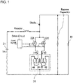
- FIG. 1 illustrates a schematic of a current balance adjustment circuit 20 according to an embodiment
- the current balance adjustment circuit 20 is provided with a coil 3A and a coil 3B.
- the coils 3A, 3B are connected in series with a switching element 22A and a switching element 22B respectively, and the switching elements are connected in parallel with an input power source 21.
- the coils 3A, 3B are arranged so that the S pole of the coil 3A and the N pole of the coil 3B are adjacent, and so that the N pole of the coil 3A and the S pole of the coil 3B are adjacent.
- the current balance adjustment circuit 20 is also provided with a coil 4A and a coil 4B.
- the coil 4A is connected in series with the coil 3A.
- the coil 4A and the coil 3A are arranged so that the S poles thereof are adjacent and the N poles thereof are adjacent.
- the coil 4B and the coil 3B are similarly connected in series.
- the coil 4B and the coil 3B are arranged so that the S poles thereof are adjacent and the N poles thereof are adjacent.
- the above described kind of current balance adjustment circuit 20 minimizes the variation by way of the induced electromotive force mutually generated between the coil 3A and the coil 3B. Therefore, the above described kind of current balance adjustment circuit 20 is capable of reducing the impact on a semiconductor device as much as possible.
- the above kind of current balance adjustment circuit 20 is such that when a surge voltage is produced in a circuit that is provided with the coil 3A and the coil 4A, the induced electromotive force mutually generated between the coil 3A and the coil 4A produces a voltage in the aforementioned circuit which is the opposite direction to the direction that the aforementioned surge voltage is applied. Therefore, it is possible to reduce a surge voltage.
- the induced electromotive force mutually generated between the coil 3B and the coil 4B similarly produces a voltage in the aforementioned circuit which is the opposite direction to the direction the aforementioned surge voltage is applied. Therefore, it is possible to reduce a surge voltage. Therefore, the impact on a semiconductor device can be reduced as much as possible.
- FIG. 1 illustrates a schematic of a current balance adjustment circuit 20 of the embodiment (one example of a "circuit” in this disclosure).
- the current balance adjustment circuit 20 is provided with a coil 3A (one example of a "first inductor part” in this disclosure) and a coil 3B (one example of a “second inductor part” in this disclosure).
- the coils 3A, 3B are connected in series to a switching element 22A (one example of a "first semiconductor element” in this disclosure) and a switching element 22B (one example of a "second semiconductor element” in this disclosure), respectively, and the switching elements are connected in parallel to an input power source 21.
- the switching elements 22A, 22B may be metal-oxide-semiconductor field-effect transistors (MOS-FETs).
- MOS-FETs metal-oxide-semiconductor field-effect transistors
- An input voltage Vin is applied between the source and drain of the switching elements 22A, 22B respectively from the input power source 21.
- These kinds of switching elements 22A, 22B control the flow of current between the source and drain by controlling the gate signal voltages respectively, to adjust the power supply supplied to the load 23 from the input power source 21.
- a magnetic field is produced in the coils 3A, 3B when a current flows in the coils 3A, 3B.
- the coils 3A, 3B are arranged so that the S pole of the magnetic field created by the coil 3A and the N pole of the magnetic field created by the coil 3B are adjacent, and the N pole of the magnetic field created by the coil 3A and the S pole of the magnetic field created by the coil 3B are adjacent (referred to below as “coupled by opposite poles").
- the arrangement of the coils 3A, 3B produces a magnetic interaction in the coils 3A, 3B.
- the current balance adjustment circuit 20 is also provided with a coil 4A (one example of a "third inductor part” in this disclosure) and a coil 4B (one example of a "fourth inductor part” in this disclosure).
- the coil 4A is connected in series with the coil 3A.
- a magnetic field is produced in the coil 4A when a current flows in the coil 4A.
- the coil 4A and the coil 3A are arranged so that the S poles of the magnetic fields created by each coil are adjacent, and the N poles of the magnetic fields created by each coil are adjacent (referred to below as "coupled by like poles").
- the arrangement of the coils 3A, 4A produces a magnetic interaction in the coils 3A, 4A.
- the coil 4B and the coil 3B are similarly connected in series.
- a magnetic field is produced in the coil 4B when a current flows in the coil 4B.
- the coil 3B and the coil 4B are arranged so that the S poles of the magnetic fields created by each coil are adjacent, and the N poles of the magnetic fields created by each coil are adjacent (referred to below as “coupled by like poles").
- the arrangement of the coils 3B, 4B produces a magnetic interaction in the coils 3B, 4B.
- An induced electromotive force responsive to the quantity of current id2 flowing in the coil 3B is also generated in the coil 3A due to the coil 3B coupled thereto by reverse poles.
- a current flows in the same direction as the direction that the quantity of current id2 flows due to the induced electromotive force.
- An induced electromotive force responsive to the quantity of current id1 flowing in the coil 3A is similarly generated in the coil 3B due to the coil 3A coupled thereto by reverse poles.
- a current flows in the same direction as the direction that the quantity of current id1 flows due to the induced electromotive force.
- the quantity of current id1 that passed through the coil 3A also flows into the coil 4A. Consequently, an electromotive force is generated in the coil 4A, producing a current of a reverse direction to the direction in which the quantity of current id1 itself is flowing.
- the size of the aforementioned electromotive force is a value responsive to the size of the quantity of current id1 that passed therethrough.
- the quantity of current id2 that passed through the coil 3B similarly flows into the coil 4B.
- an electromotive force is generated in the coil 4B, producing a current of the reverse direction to the direction in which the quantity of current id2 itself is flowing; the size of the aforementioned electromotive force is a value responsive to the size of the quantity of current id2 that passed therethrough.
- An induced electromotive force responsive to the quantity of current id1 flowing in the coil 3A is generated in the coil 4A due to the coil 3A coupled thereto by like poles (one example of the "first induced electromotive force” in this disclosure).
- the induced electromotive force causes the current to flow in the reverse direction to the direction of the quantity of current id1 flowing in the coil 4A.
- An induced electromotive force responsive to the quantity of current id2 flowing in the coil 3B is similarly generated in the coil 4B due to the coil 3B coupled thereto by like poles (one example of the "second induced electromotive force” in this disclosure).
- FIG. 2 is a diagram of a collection of electromotive forces V1-V4 which are produced in the coils 3A, 3B and the coils 4A, 4B as above described. Note that the direction of the electromotive forces V1, V3 takes the opposite direction to the direction the quantity of current id1 flows as positive. Further, the direction of the electromotive forces V2, V4 takes the opposite direction to the direction the quantity of current id2 flows as positive.
- L1-L4 are the self-inductances of the coils 3A, 3B and the coils 4A, 4B, respectively; ⁇ is the angular frequency; k1 is the magnetic coupling coefficient of the coil 3A and the coil 3B; and k2 is a magnetic coupling coefficient of the coil 3A and the coil 4A, and the coil 3B and the coil 4B.
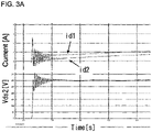
- FIG. 3 illustrates the result of simulating a time-dependent change in the quantity of current id1, the quantity of current id2, and a voltage Vds2 applied to a load 23 when a voltage is applied to the gates in the switching elements 22A, 22B respectively (referred to below as "switched on”).
- FIG. 3 compares when the current balance adjustment circuit 20 of the embodiment is connected to the switching elements 22A, 22B respectively ( FIG. 3C ), when the current balance adjustment circuit 20 is not connected to the switching elements 22A, 22B respectively ( FIG. 3A ), and when the circuit includes coils 3A, 3B but does not include the coils 4A, 4B and a current balance adjustment circuit 20A is connected to the switching elements 22A, 22B respectively ( FIG. 3B ).
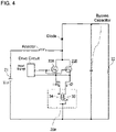
- a schematic of the current balance adjustment circuit 20A is shown, for example, in FIG. 4 .
- the quantity of current id1, quantity of current id2, and the voltage Vds2 each oscillate while gradually converging to a fixed value.
- the quantity of current id1 and the quantity of current id2 vary when the switching elements are first switched on; the convergence values thereof are also each different.
- Vds2 oscillates wildly when the switching elements are first switched on, and it can be understood therefrom that a surge voltage is generated.
- FIG. 5 illustrates a schematic of a synchronous rectifier boost chopper circuit 30.
- the synchronous rectifier boost chopper circuit 30 is provided with switching elements (22C, 22D) and switching elements (22E, 22F).
- the synchronous rectifier boost chopper circuit 30 is also provided with an input power source 21 into which an input voltage Vin enters, a reactor, a diode, a capacitor, and a load 23.
- the switching elements (22C, 22D) and the switching elements (22E, 22F) are connected respectively in parallel.
- the synchronous rectifier boost chopper circuit 30 executes switch control of each of the switching elements 22C-22F and outputs Vout which is boosted compared to Vin.
- a current balance adjustment circuit 20 is connected to the switching elements (22C, 22D) and the switching elements (22E, 22F), respectively.
- a current balance adjustment circuit 20 thus provided thereby minimizes the variation in current or the surge voltage produced in the switching elements (22C, 22D) and the switching elements (22E, 22F) respectively when a boosted Vout is output, and prevents the destruction of the synchronous rectifier boost chopper circuit 30.
- FIG. 6 illustrates a separate usage example of the current balance adjustment circuit 20.
- FIG. 6 is an example of the current balance adjustment circuit 20 used in an inverter circuit 40.
- the inverter circuit 40 is provided with an input power source 21 which inputs a DC voltage Vin.
- the switching elements (22G, 22H), the switching elements (22I, 22J), the switching elements (22K, 22L) and the switching elements (22M, 22N) are connected respectively in parallel in the inverter circuit 40.
- switch control is carried out for the switching element 22G-22N and an AC voltage Vout is output.
- the current balance adjustment circuit 20 is connected to the switching elements (22G, 22H), the switching elements (22I, 22J), the switching elements (22K, 22L) and the switching elements (22M, 22N), respectively.
- a current balance adjustment circuit 20 thus provided thereby minimizes the variation in current or the surge voltage produced in the switching elements (22G, 22H), the switching elements (22I, 22J), the switching elements (22K, 22L), and the switching elements (22M, 22N), and prevents destruction of the inverter circuit 40.
- the current balance adjustment circuit 20 may also be used in a DC/DC converter or inverter topology to thereby prevent destruction of such device machinery.
- the above-described kind of current balance adjustment circuit 20 connects a coil 3A and a coil 3B in parallel and couples the coils by reverse poles whereby the coil 3B generates an induced electromotive force in the coil 3A.
- the induced electromotive force generated by the coil 3B in the coil 3A produces a current responsive to the current id2 flowing in the switching element 22B in the direction the current id2 flows (second term in Equation (1)) in the switching element 22B.
- the coil 3A similarly generates an induced electromotive force in the coil 3B.
- the induced electromotive force generated by the coil 3A in the coil 3B produces a current responsive to the current id1 flowing in the switching element 22A in the direction the current id1 flows (second term in Equation (2)) in the switching element 22A. Therefore, the kind of variation illustrated in FIG. 3B and FIG. 3C is minimized even when there is a variation in the quantity of current id1 and quantity of current id2 flowing in each of the switching elements 22A, 22B.
- the above-described kind of current balance adjustment circuit 20 can minimize the variation in the quantity of current id1 and quantity of current id2 without providing a large impedance in the gate circuit. Therefore, the above described kind of current balance adjustment circuit 20 is capable of reducing the impact on a semiconductor device as much as possible.
- the above-described kind of current balance adjustment circuit 20 connects a coil 3A and a coil 4A in parallel and couples the coils by like poles whereby the coil 4A generates an induced electromotive force in the coil 3A.
- the induced electromotive force generated by the coil 4A in the coil 3A is in the opposite direction (the third term of Equation (1)) to the direction of the quantity of current id1 flowing in the switching element 22A, and is a size responsive to the quantity of current id1.
- the coil 3A similarly generates an induced electromotive force in the coil 4A.
- the induced electromotive force generated by the coil 3A in the coil 4A is in the opposite direction (the third term of Equation (2)) to the direction of the quantity of current id1 flowing in the switching element 22A, and is a size responsive to the quantity of current id1. That is, a large induced electromotive force is generated in a circuit connected to the switching element 22A in the opposite direction to the direction the quantity of current id1 flows when said quantity of current id1 flows compared to when the coil 3A is provided independently.
- the effect of reducing the aforementioned surge voltage increases compared to when the coil 3A is provided independently even when a surge voltage is produced in the aforementioned circuit. Further, such an effect can be verified in that, in contrast to FIG.
- the coil 3B and the coil 4B are connected in series and coupled by like poles whereby the coil 4B generates an induced electromotive force in the coil 3B.
- the induced electromotive force generated by the coil 4B in the coil 3B is in the opposite direction (the third term of Equation (2)) to the direction of the quantity of current id2 flowing in the switching element 22B, and is a size responsive to the quantity of current id2.
- the coil 3B similarly generates an induced electromotive force in the coil 4B.
- the induced electromotive force generated by the coil 3B in the coil 4B is in the opposite direction (the second term of Equation (4)) to the direction of the quantity of current id2 flowing in the switching element 22B, and is a size responsive to the quantity of current id2. That is, a large induced electromotive force is generated in a circuit connected to the switching element 22B in the opposite direction to the direction the quantity of current id2 flows when said quantity of current id2 flows compared to when the coil 3B is provided independently.
- the effect of reducing the aforementioned surge voltage increases compared to when the coil 3B is provided independently even when a surge voltage is produced in the aforementioned circuit. Further, such an effect can be verified in that, in contrast to FIG.
- the current balance adjustment circuit 20 in this embodiment is described as one example of a "semiconductor circuit" of this disclosure.
- the current balance adjustment circuit 20A may also serve as one example of a “semiconductor circuit” of this disclosure.
- This kind of current balance adjustment circuit 20A also provides the effect of minimizing the variation in the quantity of current id1 and quantity of current id2 as illustrated in FIG. 3B .
- a current balance adjustment circuit 20B according to a first modification example is provided with a metal-insulator-metal (MIM) substrate 5.
- the current balance adjustment circuit 20B uses the parasitic inductance contained in the MIM substrate 5 as a substitute for the coils 3A, 3B and the coils 4A, 4B. More specifically, the parasitic inductance contained in the MIM substrate 5 is utilized to implement the current variation minimizing function and the surge voltage minimizing function achieved by the coils 3A, 3B and the coils 4A, 4B.
- the above-described kind of current balance adjustment circuit 20B exhibits the same effects as the current balance adjustment circuit 20. Further, the coils 3A, 3B and the coils 4A, 4B are not provided in the current balance adjustment circuit 20B; therefore, the reduction in the number of parts simplifies the manufacturing process, reduces the parts management cost, or allows for achieving more economical parts costs.
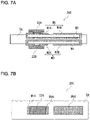
- FIG. 7 illustrate a schematic of a current balance adjustment circuit 20C according to a second modification example.
- FIG. 7A is a schematic cross-sectional view of the current balance adjustment circuit 20C
- FIG. 7B is a schematic top view of the current balance adjustment circuit 20C.
- the current balance adjustment circuit 20C is provided with a MIM substrate 5A.
- the MIM substrate 5A is formed from four metal layers (M1-M4), with an insulating material provided between the metal layers.
- the M1 layer of the MIM substrate 5A forms the front surface of the MIM substrate 5A (one example of a "third metal layer" in this disclosure).
- the M1 layer is divided by the insulating material into two regions (M1A, M1B; M1A is one example of a "first portion” in this disclosure, and M1B is an example of a "second portion” in this disclosure); a switching element 22A is mounted on one region M1A.
- An M2 layer (one example of a "first metal layer” in this disclosure) is provided facing the M1 layer with the insulating material sandwiched therebetween.
- the M2 layer, and M1A of the M1 layer are connected in series.
- the M2 layer and M1B are also connected in series.
- the M3 layer and M4 layers are structured identically to the M1 layer and the M2 layer. That is, the M3 layer forms the rear surface of the MIM substrate 5A (one example of a "fourth metal layer” in this disclosure).
- the M3 layer is divided by the insulating material into two regions (M3A, M3B; M3A is one example of a "third portion” in this disclosure, and M3B is an example of a "fourth portion” in this disclosure); a switching element 22B is mounted on one region M3A.
- An M4 layer (one example of a "second metal layer” in this disclosure) is provided facing the M3 layer with the insulating material sandwiched therebetween. The M4 layer, and the M3A of the M3 layer are connected in series.
- the M4 layer, and the M3B of the M3 layer are also connected in series.
- the M4 layer is provided facing the M2 layer with the insulating material sandwiched therebetween.
- the M4 layer and the M2 layer are electrically connected.
- the M2 layer and M4 layer are one example of a "prescribed metal layer pair" in this disclosure.
- M2 layer and the M4 layer facing each other with the insulating material sandwiched therebetween creates a magnetic coupling between the M2 layer and the M4 layer.
- the M2 layer is a substitute for the coil 3A
- the M4 layer is a substitute for the coil 3B.
- providing the M1 layer and the M2 layer facing each other with the insulating material sandwiched therebetween creates a magnetic coupling between M1B of the M1 layer and the M2 layer.
- M1B is a substitute for the coil 4A.
- M3B is a substitute for the coil 4B.
- the above-described kind of current balance adjustment circuit 20C exhibits the same effects as the current balance adjustment circuit 20. Further, the coils 3A, 3B and the coils 4A, 4B are not provided in the current balance adjustment circuit 20C; therefore, the reduction in the number of parts simplifies the manufacturing process, reduces the parts management cost, or allows for achieving more economical parts costs.
- the semiconductor circuit (20C) described in Supplemental Note 3 including: a plurality of metal layers which are stacked, and an insulating part provided between the plurality of metal layers; and
Landscapes
- Engineering & Computer Science (AREA)
- Power Engineering (AREA)
- Semiconductor Integrated Circuits (AREA)
- Power Conversion In General (AREA)
- Electronic Switches (AREA)
- Coils Or Transformers For Communication (AREA)
Abstract
Description
- The present invention relates to a semiconductor circuit.
- There is disclosed a semiconductor device in which a plurality of semiconductor elements is connected in parallel (for example, Patent Documents 1-2).
-
- [Patent Document 1]
Japanese Patent No. 3421544 - [Patent Document 2]
Japanese Patent Publication No. 2017-175602 - A plurality of semiconductor elements may be caused to each perform a switching operation by applying a gate voltage to each of the semiconductor elements. In this case, the size of the drain current flowing in the semiconductor elements may be varied. Therefore, for instance,
Patent Document 1 provides a source inductance that is shared between a gate circuit and a main circuit in which the respective semiconductor elements are arranged. This kind of common source inductance generates an electromotive force in accordance with the size of the drain current flowing in the semiconductor element, with the electromotive force producing a current flowing in the reverse of the direction of said drain current. The gate voltage on a semiconductor element is adjusted so that the electromotive force generated minimizes the variation in the size of the drain current. -
Patent Document 2, for example, also mutually couples the inductance of a gate node in one semiconductor element and the inductance of a drain node in another semiconductor element. In the case of such a structure, the coupled portion generates an electromotive force in accordance with the size of the drain current flowing in the semiconductor element with the electromotive force producing a current flowing in the reverse of the direction of said drain current. Therefore, if the size of the drain current in one semiconductor element is greater than the size of the drain current in another semiconductor element, for example, the gate voltage of the other semiconductor element may be adjusted to increase the size of the drain current flowing in the other semiconductor element. The variation in the size of the drain current flowing in the semiconductor elements may thus be minimized. - The above kind of method for minimizing the variation in the drain currents suggests providing a larger impedance to the gate circuit and the main circuit in order to be able to handle any sharp drain current. However, providing a larger impedance suggests that a sharp noise may also be generated in the gate circuit caused by the sharp drain current in the main circuit. Accordingly, this suggests that the switching operation of a semiconductor element may cause a malfunction to occur. If the switching of a semiconductor element is a malfunction, this suggests that a current exceeding the breakdown voltage of the semiconductor element may flow in a circuit in a semiconductor device and destroy the device. This also suggests that a large deviation may occur in the power loss when switching a semiconductor element where the switching operation is malfunctioning, and this may likely have a large impact on the heat generated in or the operating life of the semiconductor device.
- In view of the above situation, the present invention aims to reduce as much as possible the impact on a semiconductor device when minimizing the variation in the size of the current flowing in each semiconductor element of a semiconductor device containing the aforementioned semiconductor elements connected in parallel.
- To address the above described disadvantages, the present invention adopts the following configurations.
- That is, a semiconductor circuit according to one aspect of the present invention includes: a first inductor part configured to connect in series with a source electrode of a first semiconductor element; and a second inductor part configured to connect in series with a source electrode in a second semiconductor element that is configured to connect in parallel with the first semiconductor element; the first inductor part and the second inductor part are arranged to generate an induced electromotive force in the first inductor part and the second inductor part by way of a magnetic interaction, so that the currents flowing in the first inductor part and the second inductor part are reinforced in the same direction.
- The aforementioned configuration minimizes the variation by way of the induced electromotive force mutually generated between the first inductor and the second inductor, even when there is a variation in the quantity of current flowing in the first semiconductor element and the second semiconductor element. The aforementioned configuration also achieves minimizing the variation in the quantity of current without needing to provide a large impedance to the gate circuit. Therefore, the aforementioned configuration reduces the impact on a semiconductor device as much as possible.
- The semiconductor circuit according to the above one aspect may further include: a third inductor part configured to connect in series with the first inductor part; and a fourth inductor part configured to connect in series with the second inductor part; wherein the third inductor part is arranged to produce a voltage by way of a first induced electromotive force generated due to a magnetic interaction originating from the first inductor part, said voltage of an opposite direction to the voltage applied to the third inductor part itself, and to produce a voltage in the first inductor part by way of the first induced electromotive force generated due to a magnetic interaction from the third inductor part itself, said voltage of an opposite direction to the voltage applied to the first inductor part; and the fourth inductor part is arranged to produce a voltage by way of a second induced electromotive force generated due to a magnetic interaction originating from the second inductor part, said voltage of an opposite direction to the voltage applied to the fourth inductor part itself, and to produce a voltage in the second inductor part by way of the second induced electromotive force generated due to a magnetic interaction from the fourth inductor part itself, said voltage of an opposite direction to the voltage applied to the second inductor part.
- The aforementioned configuration is such that when a surge voltage is produced in a circuit that is provided with the first inductor part and the third inductor part, the induced electromotive force mutually generated between the first inductor part and the third inductor part produces a voltage in the aforementioned circuit which is the opposite direction to the direction that the aforementioned surge voltage is applied. Therefore, it is possible to reduce a surge voltage. When a surge voltage is produced in a circuit that is provided with the second inductor part and the fourth inductor part, the induced electromotive force mutually generated between the second inductor part and the fourth inductor part similarly produces a voltage in the aforementioned circuit which is the opposite direction to the direction the aforementioned surge voltage is applied. Therefore, it is possible to reduce a surge voltage. Therefore, the impact on a semiconductor device can be reduced as much as possible.
- The semiconductor circuit according to the above one aspect may be such that at least one of the first inductor part, second inductor part, third inductor part, and fourth inductor part includes a parasitic inductance.
- The aforementioned configuration is such that there is no need to provide parts that generate a mutually induced electromotive force for minimizing the variation in the quantity of current or reducing the surge voltage. Therefore, the number of parts needed to create the circuit is reduced. Therefore, this simplifies the process for manufacturing the circuit, decreases the cost of maintaining parts, or reduces the parts cost, etc.
- The semiconductor circuit according to the above one aspect may include: a plurality of metal layers which are stacked, and an insulating part provided between the plurality of metal layers; and a prescribed pair of facing metal layers from among the plurality of stacked metal layers is electrically connected in parallel; and the prescribed pair of metal layers is the first inductor part and the second inductor part.
- The aforementioned configuration is such that an induced electromotive force is mutually generated in a prescribed pair of metal layers respectively to minimize the variation in the quantity of current flowing through said prescribed pair of metal layers. In other words, there is no need to provide parts for generating a mutually induced electromotive force for minimizing the variation in the quantity of current. Therefore, the number of parts needed to create the circuit is reduced. Therefore, this simplifies the process for manufacturing the circuit, decreases the cost of maintaining parts, or reduces the parts cost, etc.
- The semiconductor circuit according to the above one aspect may be such that the prescribed pair of metal layers is formed from a first metal layer and a second metal layer; a third metal layer facing the first metal layer is divided into a first portion and a second portion by the insulating part; the first portion, the first metal layer, and the second portion are electrically connected in series; a fourth metal layer facing the second metal layer is divided into a third portion and a fourth portion by the insulating part; the third portion, the second metal layer, and the fourth portion are electrically connected in series; the first metal layer is the first inductor part; the second metal layer is the second inductor part; the second portion of the third metal layer is the third inductor part; and the fourth portion of the fourth metal layer is the fourth inductor part.
- The aforementioned configuration is such that when a surge voltage is generated in the first portion of the third metal layer, the first metal layer, and the second portion of the third metal layer which are connected in series, an induced electromotive force is generated in the first metal layer and the second portion of the third metal layer in the reverse direction of the direction the surge voltage is applied. Therefore, it is possible to reduce the aforementioned surge voltage. When a surge voltage is generated in the third portion of the fourth metal layer, the second metal layer, and the fourth portion of the fourth metal layer which are connected in series, similarly an induced electromotive force is mutually generated in the second metal layer and the fourth portion of the fourth metal layer in the reverse direction of the direction the surge voltage is applied. Therefore, it is possible to reduce the aforementioned surge voltage. In other words, the semiconductor elements are mounted on the first portion of the third metal layer and the third portion of the fourth metal layer, and there is no need to provide parts for generating a mutually generated electromotive force for reducing the surge voltage when a current flows through the semiconductor elements. Therefore, the number of parts needed to create the circuit is reduced. Therefore, this simplifies the process for manufacturing the circuit, decreases the cost of maintaining parts, or reduces the parts cost, etc.
- The means in the present invention for addressing the above disadvantages may be combined as appropriate and used.
- The present invention can reduce as much as possible the impact on a semiconductor device when minimizing the variation in the size of the current flowing in each semiconductor element of a semiconductor device containing the aforementioned semiconductor elements connected in parallel.
-
-
FIG. 1 illustrates a schematic of a current balance adjustment circuit according to an embodiment; -
FIG. 2 illustrates one example of an electromotive force generated in a coil; -
FIG. 3 illustrates the result of simulating a time-dependent change in the quantity of current and the voltage when a voltage is applied to the gates of the switching elements; -
FIG. 4 illustrates a schematic of a current balance adjustment circuit without some coils; -
FIG. 5 illustrates a first use example of a current balance adjustment circuit; -
FIG. 6 illustrates a second use example of a current balance adjustment circuit; and -
FIG. 7 illustrates a schematic of a current balance adjustment circuit according to a second modification example. - An example application of the present invention is described in detail below with reference to the drawings.
FIG. 1 illustrates a schematic of a currentbalance adjustment circuit 20 according to an embodiment; the currentbalance adjustment circuit 20 is provided with acoil 3A and acoil 3B. Thecoils switching element 22A and aswitching element 22B respectively, and the switching elements are connected in parallel with aninput power source 21. Thecoils coil 3A and the N pole of thecoil 3B are adjacent, and so that the N pole of thecoil 3A and the S pole of thecoil 3B are adjacent. - The current
balance adjustment circuit 20 is also provided with a coil 4A and a coil 4B. The coil 4A is connected in series with thecoil 3A. The coil 4A and thecoil 3A are arranged so that the S poles thereof are adjacent and the N poles thereof are adjacent. The coil 4B and thecoil 3B are similarly connected in series. The coil 4B and thecoil 3B are arranged so that the S poles thereof are adjacent and the N poles thereof are adjacent. - Even when there is a variation in the quantity of current id1 and the quantity of current id2 flowing in the
switching elements balance adjustment circuit 20 minimizes the variation by way of the induced electromotive force mutually generated between thecoil 3A and thecoil 3B. Therefore, the above described kind of currentbalance adjustment circuit 20 is capable of reducing the impact on a semiconductor device as much as possible. - The above kind of current
balance adjustment circuit 20 is such that when a surge voltage is produced in a circuit that is provided with thecoil 3A and the coil 4A, the induced electromotive force mutually generated between thecoil 3A and the coil 4A produces a voltage in the aforementioned circuit which is the opposite direction to the direction that the aforementioned surge voltage is applied. Therefore, it is possible to reduce a surge voltage. When a surge voltage is produced in a circuit that is provided with thecoil 3B and the coil 4B, the induced electromotive force mutually generated between thecoil 3B and the coil 4B similarly produces a voltage in the aforementioned circuit which is the opposite direction to the direction the aforementioned surge voltage is applied. Therefore, it is possible to reduce a surge voltage. Therefore, the impact on a semiconductor device can be reduced as much as possible. - An embodiment of the present invention is described next with reference to the drawings.
-
FIG. 1 illustrates a schematic of a currentbalance adjustment circuit 20 of the embodiment (one example of a "circuit" in this disclosure). The currentbalance adjustment circuit 20 is provided with acoil 3A (one example of a "first inductor part" in this disclosure) and acoil 3B (one example of a "second inductor part" in this disclosure). Thecoils switching element 22A (one example of a "first semiconductor element" in this disclosure) and aswitching element 22B (one example of a "second semiconductor element" in this disclosure), respectively, and the switching elements are connected in parallel to aninput power source 21. Here, theswitching elements switching elements input power source 21. These kinds of switchingelements load 23 from theinput power source 21. A magnetic field is produced in thecoils coils coils coil 3A and the N pole of the magnetic field created by thecoil 3B are adjacent, and the N pole of the magnetic field created by thecoil 3A and the S pole of the magnetic field created by thecoil 3B are adjacent (referred to below as "coupled by opposite poles"). Thus, the arrangement of thecoils coils - The current
balance adjustment circuit 20 is also provided with a coil 4A (one example of a "third inductor part" in this disclosure) and a coil 4B (one example of a "fourth inductor part" in this disclosure). The coil 4A is connected in series with thecoil 3A. A magnetic field is produced in the coil 4A when a current flows in the coil 4A. The coil 4A and thecoil 3A are arranged so that the S poles of the magnetic fields created by each coil are adjacent, and the N poles of the magnetic fields created by each coil are adjacent (referred to below as "coupled by like poles"). Thus, the arrangement of thecoils 3A, 4A produces a magnetic interaction in thecoils 3A, 4A. The coil 4B and thecoil 3B are similarly connected in series. A magnetic field is produced in the coil 4B when a current flows in the coil 4B. Thecoil 3B and the coil 4B are arranged so that the S poles of the magnetic fields created by each coil are adjacent, and the N poles of the magnetic fields created by each coil are adjacent (referred to below as "coupled by like poles"). Thus, the arrangement of thecoils 3B, 4B produces a magnetic interaction in thecoils 3B, 4B. - When a voltage is applied to the gates of each of the above-described
switching elements coil 3A from the switchingelement 22A. An electromotive force is generated in thecoil 3A, producing a current of the reverse direction to the direction in which the quantity of current id1 itself is flowing. A quantity of current id2 similarly flows to thecoil 3B from the switchingelement 22B. An electromotive force is generated in thecoil 3B, producing a current of the reverse direction to the direction in which the quantity of current id2 itself is flowing. - An induced electromotive force responsive to the quantity of current id2 flowing in the
coil 3B is also generated in thecoil 3A due to thecoil 3B coupled thereto by reverse poles. A current flows in the same direction as the direction that the quantity of current id2 flows due to the induced electromotive force. An induced electromotive force responsive to the quantity of current id1 flowing in thecoil 3A is similarly generated in thecoil 3B due to thecoil 3A coupled thereto by reverse poles. A current flows in the same direction as the direction that the quantity of current id1 flows due to the induced electromotive force. - The quantity of current id1 that passed through the
coil 3A also flows into the coil 4A. Consequently, an electromotive force is generated in the coil 4A, producing a current of a reverse direction to the direction in which the quantity of current id1 itself is flowing. The size of the aforementioned electromotive force is a value responsive to the size of the quantity of current id1 that passed therethrough. The quantity of current id2 that passed through thecoil 3B similarly flows into the coil 4B. Consequently, an electromotive force is generated in the coil 4B, producing a current of the reverse direction to the direction in which the quantity of current id2 itself is flowing; the size of the aforementioned electromotive force is a value responsive to the size of the quantity of current id2 that passed therethrough. - An induced electromotive force responsive to the quantity of current id1 flowing in the
coil 3A is generated in the coil 4A due to thecoil 3A coupled thereto by like poles (one example of the "first induced electromotive force" in this disclosure). The induced electromotive force causes the current to flow in the reverse direction to the direction of the quantity of current id1 flowing in the coil 4A. An induced electromotive force responsive to the quantity of current id2 flowing in thecoil 3B is similarly generated in the coil 4B due to thecoil 3B coupled thereto by like poles (one example of the "second induced electromotive force" in this disclosure). The induced electromotive force causes the current to flow in the reverse direction to the direction of the quantity of current id2 flowing in the coil 4B.FIG. 2 is a diagram of a collection of electromotive forces V1-V4 which are produced in thecoils - Here, L1-L4 are the self-inductances of the
coils coil 3A and thecoil 3B; and k2 is a magnetic coupling coefficient of thecoil 3A and the coil 4A, and thecoil 3B and the coil 4B. -
FIG. 3 illustrates the result of simulating a time-dependent change in the quantity of current id1, the quantity of current id2, and a voltage Vds2 applied to aload 23 when a voltage is applied to the gates in theswitching elements FIG. 3 compares when the currentbalance adjustment circuit 20 of the embodiment is connected to theswitching elements FIG. 3C ), when the currentbalance adjustment circuit 20 is not connected to theswitching elements FIG. 3A ), and when the circuit includescoils balance adjustment circuit 20A is connected to theswitching elements FIG. 3B ). A schematic of the currentbalance adjustment circuit 20A is shown, for example, inFIG. 4 . - As illustrated in
FIG. 3A , in the case where a currentbalance adjustment circuit 20 is not connected, when theswitching elements - Meanwhile, as illustrated in
FIG. 3B , when coils 3A, 3B are present, the coils 4A, 4B are not present, and a currentbalance adjustment circuit 20A is connected, the variation of the quantity of current id1 and quantity of current id2 is minimized compared toFIG. 3A . The difference in the convergence value of the quantity of current id1 and the convergence value of the quantity of current id2 also decreases. Therefore, coupling thecoils FIG. 2 can be said to be effective for minimizing the variation between the quantity of current id1 and the quantity of current id2. - As illustrated in
FIG. 3C , when a currentbalance adjustment circuit 20 is connected, the variation in the quantity of current id1 and the quantity of current id2 is minimized similarly toFIG. 3B . The difference in the convergence value of the quantity of current id1 and the convergence value of the quantity of current id2 also decreases. Further, inFIG. 3C , the oscillation of voltage Vds2 is small when the switching elements are first switched on and the voltage Vds2 quickly converges to a fixed value. Therefore, coupling thecoil 3A and the coil 4A, and thecoil 3B and the coil 4B by like poles can be said to have the effect of minimizing oscillation (surge voltage) in Vds2. In other words, the third terms on the right sides of the Equation (1) and the Equation (2), respectively and the second terms on the right sides of the Equation (3) and the Equation (4), respectively, can be said to be effective for minimizing a surge voltage. - A usage example for the current
balance adjustment circuit 20 is described next.FIG. 5 illustrates a schematic of a synchronous rectifierboost chopper circuit 30. The synchronous rectifierboost chopper circuit 30 is provided with switching elements (22C, 22D) and switching elements (22E, 22F). The synchronous rectifierboost chopper circuit 30 is also provided with aninput power source 21 into which an input voltage Vin enters, a reactor, a diode, a capacitor, and aload 23. The switching elements (22C, 22D) and the switching elements (22E, 22F) are connected respectively in parallel. When an input voltage Vin enters therein from theinput power source 21, the synchronous rectifierboost chopper circuit 30 executes switch control of each of the switching elements 22C-22F and outputs Vout which is boosted compared to Vin. A currentbalance adjustment circuit 20 is connected to the switching elements (22C, 22D) and the switching elements (22E, 22F), respectively. A currentbalance adjustment circuit 20 thus provided thereby minimizes the variation in current or the surge voltage produced in the switching elements (22C, 22D) and the switching elements (22E, 22F) respectively when a boosted Vout is output, and prevents the destruction of the synchronous rectifierboost chopper circuit 30. -
FIG. 6 illustrates a separate usage example of the currentbalance adjustment circuit 20.FIG. 6 is an example of the currentbalance adjustment circuit 20 used in aninverter circuit 40. Theinverter circuit 40 is provided with aninput power source 21 which inputs a DC voltage Vin. The switching elements (22G, 22H), the switching elements (22I, 22J), the switching elements (22K, 22L) and the switching elements (22M, 22N) are connected respectively in parallel in theinverter circuit 40. When a DC voltage Vin is applied from theinput power source 21 to theinverter circuit 40 thus configured, switch control is carried out for theswitching element 22G-22N and an AC voltage Vout is output. - The current
balance adjustment circuit 20 is connected to the switching elements (22G, 22H), the switching elements (22I, 22J), the switching elements (22K, 22L) and the switching elements (22M, 22N), respectively. A currentbalance adjustment circuit 20 thus provided thereby minimizes the variation in current or the surge voltage produced in the switching elements (22G, 22H), the switching elements (22I, 22J), the switching elements (22K, 22L), and the switching elements (22M, 22N), and prevents destruction of theinverter circuit 40. - Outside of the usage examples in
FIG. 5 andFIG. 6 , the currentbalance adjustment circuit 20 may also be used in a DC/DC converter or inverter topology to thereby prevent destruction of such device machinery. - The above-described kind of current
balance adjustment circuit 20 connects acoil 3A and acoil 3B in parallel and couples the coils by reverse poles whereby thecoil 3B generates an induced electromotive force in thecoil 3A. The induced electromotive force generated by thecoil 3B in thecoil 3A produces a current responsive to the current id2 flowing in theswitching element 22B in the direction the current id2 flows (second term in Equation (1)) in theswitching element 22B. Thecoil 3A similarly generates an induced electromotive force in thecoil 3B. The induced electromotive force generated by thecoil 3A in thecoil 3B produces a current responsive to the current id1 flowing in theswitching element 22A in the direction the current id1 flows (second term in Equation (2)) in theswitching element 22A. Therefore, the kind of variation illustrated inFIG. 3B andFIG. 3C is minimized even when there is a variation in the quantity of current id1 and quantity of current id2 flowing in each of theswitching elements balance adjustment circuit 20 can minimize the variation in the quantity of current id1 and quantity of current id2 without providing a large impedance in the gate circuit. Therefore, the above described kind of currentbalance adjustment circuit 20 is capable of reducing the impact on a semiconductor device as much as possible. - The above-described kind of current
balance adjustment circuit 20 connects acoil 3A and a coil 4A in parallel and couples the coils by like poles whereby the coil 4A generates an induced electromotive force in thecoil 3A. The induced electromotive force generated by the coil 4A in thecoil 3A is in the opposite direction (the third term of Equation (1)) to the direction of the quantity of current id1 flowing in theswitching element 22A, and is a size responsive to the quantity of current id1. Thecoil 3A similarly generates an induced electromotive force in the coil 4A. The induced electromotive force generated by thecoil 3A in the coil 4A is in the opposite direction (the third term of Equation (2)) to the direction of the quantity of current id1 flowing in theswitching element 22A, and is a size responsive to the quantity of current id1. That is, a large induced electromotive force is generated in a circuit connected to theswitching element 22A in the opposite direction to the direction the quantity of current id1 flows when said quantity of current id1 flows compared to when thecoil 3A is provided independently. In other words, the effect of reducing the aforementioned surge voltage increases compared to when thecoil 3A is provided independently even when a surge voltage is produced in the aforementioned circuit. Further, such an effect can be verified in that, in contrast toFIG. 3B , inFIG. 3C , the oscillation of voltage Vds2 is small when the switching elements are first switched on and the voltage Vds2 quickly converges to a fixed value. Therefore, the impact on a semiconductor device can be reduced as much as possible. - In the same manner, the
coil 3B and the coil 4B are connected in series and coupled by like poles whereby the coil 4B generates an induced electromotive force in thecoil 3B. The induced electromotive force generated by the coil 4B in thecoil 3B is in the opposite direction (the third term of Equation (2)) to the direction of the quantity of current id2 flowing in theswitching element 22B, and is a size responsive to the quantity of current id2. Thecoil 3B similarly generates an induced electromotive force in the coil 4B. The induced electromotive force generated by thecoil 3B in the coil 4B is in the opposite direction (the second term of Equation (4)) to the direction of the quantity of current id2 flowing in theswitching element 22B, and is a size responsive to the quantity of current id2. That is, a large induced electromotive force is generated in a circuit connected to theswitching element 22B in the opposite direction to the direction the quantity of current id2 flows when said quantity of current id2 flows compared to when thecoil 3B is provided independently. In other words, the effect of reducing the aforementioned surge voltage increases compared to when thecoil 3B is provided independently even when a surge voltage is produced in the aforementioned circuit. Further, such an effect can be verified in that, in contrast toFIG. 3B , inFIG. 3C , the oscillation of voltage Vds2 is small when the switching elements are first switched on and the voltage Vds2 quickly converges to a fixed value. Therefore, the impact on a semiconductor device can be reduced as much as possible. - The current
balance adjustment circuit 20 in this embodiment is described as one example of a "semiconductor circuit" of this disclosure. However, the currentbalance adjustment circuit 20A may also serve as one example of a "semiconductor circuit" of this disclosure. This kind of currentbalance adjustment circuit 20A also provides the effect of minimizing the variation in the quantity of current id1 and quantity of current id2 as illustrated inFIG. 3B . - While an embodiment of the present invention is described above in detail, all points in the previous description are merely examples of the present invention. It goes without saying that various modifications and variations are possible without departing from the scope of the invention. For instance, the following modification is possible. Note that constituent elements that are identical to the constituent elements in the above described embodiment are given the same reference numerals and where appropriate, a description of features that are identical to the above embodiment are omitted. The following modifications may be combined as appropriate.
- 3.1 A current balance adjustment circuit 20B according to a first modification example is provided with a metal-insulator-metal (MIM) substrate 5. The current balance adjustment circuit 20B uses the parasitic inductance contained in the MIM substrate 5 as a substitute for the
coils coils balance adjustment circuit 20. Further, thecoils - 3.2
FIG. 7 illustrate a schematic of a current balance adjustment circuit 20C according to a second modification example.FIG. 7A is a schematic cross-sectional view of the current balance adjustment circuit 20C, andFIG. 7B is a schematic top view of the current balance adjustment circuit 20C. As illustrated inFIG. 7 , the current balance adjustment circuit 20C is provided with aMIM substrate 5A. TheMIM substrate 5A is formed from four metal layers (M1-M4), with an insulating material provided between the metal layers. The M1 layer of theMIM substrate 5A forms the front surface of theMIM substrate 5A (one example of a "third metal layer" in this disclosure). The M1 layer is divided by the insulating material into two regions (M1A, M1B; M1A is one example of a "first portion" in this disclosure, and M1B is an example of a "second portion" in this disclosure); aswitching element 22A is mounted on one region M1A. An M2 layer (one example of a "first metal layer" in this disclosure) is provided facing the M1 layer with the insulating material sandwiched therebetween. The M2 layer, and M1A of the M1 layer are connected in series. The M2 layer and M1B are also connected in series. - The M3 layer and M4 layers are structured identically to the M1 layer and the M2 layer. That is, the M3 layer forms the rear surface of the
MIM substrate 5A (one example of a "fourth metal layer" in this disclosure). The M3 layer is divided by the insulating material into two regions (M3A, M3B; M3A is one example of a "third portion" in this disclosure, and M3B is an example of a "fourth portion" in this disclosure); aswitching element 22B is mounted on one region M3A. An M4 layer (one example of a "second metal layer" in this disclosure) is provided facing the M3 layer with the insulating material sandwiched therebetween. The M4 layer, and the M3A of the M3 layer are connected in series. The M4 layer, and the M3B of the M3 layer are also connected in series. The M4 layer is provided facing the M2 layer with the insulating material sandwiched therebetween. Although not illustrated, the M4 layer and the M2 layer are electrically connected. The M2 layer and M4 layer are one example of a "prescribed metal layer pair" in this disclosure. - For this kind of current balance adjustment circuit 20C, providing the M2 layer and the M4 layer facing each other with the insulating material sandwiched therebetween creates a magnetic coupling between the M2 layer and the M4 layer. In other words, the M2 layer is a substitute for the
coil 3A and the M4 layer is a substitute for thecoil 3B. Further, providing the M1 layer and the M2 layer facing each other with the insulating material sandwiched therebetween creates a magnetic coupling between M1B of the M1 layer and the M2 layer. In other words, M1B is a substitute for the coil 4A. Further, providing the M1 layer and the M2 layer facing each other with the insulating material sandwiched therebetween creates a magnetic coupling between M1B of the M1 layer and the M2 layer. In other words, M3B is a substitute for the coil 4B. - The above-described kind of current balance adjustment circuit 20C exhibits the same effects as the current
balance adjustment circuit 20. Further, thecoils - The embodiment and modification examples heretofore disclosed may each be combined.
- To allow for comparisons between the constituent elements of the present invention and the configuration in the embodiment, the constituent elements of the invention are described together with reference numerals in the drawings.
- A semiconductor circuit (20, 20A, 20B, 20C) including: a first inductor part (3A, M2) configured to connect in series with a source electrode of a first semiconductor element (22A); and
- a second inductor part (3B, M4) configured to connect in series with a source electrode in a second semiconductor element (22B) that is configured to connect in parallel to the first semiconductor element (22A);
- the first inductor part (3A, M2) and the second inductor part (3B, M4) are arranged to generate an induced electromotive force in the first inductor part (3A, M2) and the second inductor part (3B, M4) by way of a magnetic interaction, so that the currents flowing in the first inductor part (3A, M2) and the second inductor part (3B, M4) are reinforced in the same direction.
- The semiconductor circuit (20, 20A, 20B, 20C) described in
Supplemental Note 1, further including: a third inductor part (4A, M1B) configured to connect in series with the first inductor part (3A, M2); and - a fourth inductor part (4B, M3B) configured to connect in series with the second inductor part (3B, M4); wherein
- the third inductor part (4A, M1B) is arranged to produce a voltage by way of a first induced electromotive force generated due to a magnetic interaction originating from the first inductor part (3A, M2), said voltage of an opposite direction to the voltage applied to the third inductor part (4A, M1B) itself, and to produce a voltage in the first inductor part (3A, M2) by way of the first induced electromotive force generated due to a magnetic interaction from the third inductor part (4A, M1B) itself, said voltage of an opposite direction to the voltage applied to the first inductor part (3A, M2); and
- the fourth inductor part (4B, M3B) is arranged to produce a voltage by way of a second induced electromotive force generated due to a magnetic interaction originating from the second inductor part (3B, M4), said voltage of an opposite direction to the voltage applied to the fourth inductor part (4B, M3B) itself, and to produce a voltage in the second inductor part by way of the second induced electromotive force generated due to a magnetic interaction from the fourth inductor part (4B, M3B) itself, said voltage of an opposite direction to the voltage applied to the second inductor part (3B, M4).
- The semiconductor circuit (20, 20A, 20B, 20C) described in
Supplemental Note - The semiconductor circuit (20C) described in
Supplemental Note 3, including: a plurality of metal layers which are stacked, and an insulating part provided between the plurality of metal layers; and - a prescribed pair of facing metal layers (M2, M4) from among the plurality of stacked metal layers is electrically connected in parallel; and
- the prescribed pair of metal layers (M2, M4) is the first inductor part (M2) and the second inductor part (M4).
- The semiconductor circuit (20C) described in
Supplemental Note 4, wherein the prescribed pair of metal layers (M2, M4) is formed from a first metal layer (M2) and a second metal layer (M4); - a third metal layer (M1) facing the first metal layer (M2) is divided into a first portion (M1A) and a second portion (M1B) by the insulating part;
- the first portion (M1A), the first metal layer (M2), and the second portion (M1B) are electrically connected in series;
- a fourth metal layer (M3) facing the second metal layer (M4) is divided into a third portion (M3A) and a fourth portion (M3B) by the insulating part;
- the third portion (M3A), the second metal layer (M4), and the fourth portion (M3B) are electrically connected in series;
- the first metal layer (M2) is the first inductor part (M2);
- the second metal layer (M4) is the second inductor part (M4);
- the second portion (M1B) of the third metal layer (M1) is the third inductor part (M1B); and
- the fourth portion (M3B) of the fourth metal layer (M3) is the fourth inductor part (M3B).
-
- 3A, 3B:
- Coil
- 4A, 4B:
- Coil
- 5, 5A:
- Substrate
- 20, 20A, 20B, 20C:
- Current balance adjustment circuit
- 21:
- Input power source
- 22A-22N:
- Switching element
- 23:
- Load
- 30:
- Synchronous rectifier boost chopper circuit
- 40:
- Inverter circuit
Claims (5)
- A semiconductor circuit comprising: a first inductor part configured to connect in series with a source electrode of a first semiconductor element; anda second inductor part configured to connect in series with a source electrode in a second semiconductor element that is configured to connect in parallel to the first semiconductor element;the first inductor part and the second inductor part are arranged to generate an induced electromotive force in the first inductor part and the second inductor part by way of a magnetic interaction, so that the currents flowing in the first inductor part and the second inductor part are reinforced in the same direction.
- The semiconductor circuit according to claim 1, further comprising: a third inductor part configured to connect in series with the first inductor part; anda fourth inductor part configured to connect in series with the second inductor part; whereinthe third inductor part is arranged to produce a voltage by way of a first induced electromotive force generated due to a magnetic interaction originating from the first inductor part, said voltage of an opposite direction to the voltage applied to the third inductor part itself, and to produce a voltage in the first inductor part by way of the first induced electromotive force generated due to a magnetic interaction from the third inductor part itself, said voltage of an opposite direction to the voltage applied to the first inductor part; andthe fourth inductor part is arranged to produce a voltage by way of a second induced electromotive force generated due to a magnetic interaction originating from the second inductor part, said voltage of an opposite direction to the voltage applied to the fourth inductor part itself, and to produce a voltage in the second inductor part by way of the second induced electromotive force generated due to a magnetic interaction from the fourth inductor part itself, said voltage of an opposite direction to the voltage applied to the second inductor part.
- The semiconductor circuit according to claims 1 or 2, wherein at least one of the first inductor part, second inductor part, third inductor part, and fourth inductor part includes a parasitic inductance.
- The semiconductor circuit according to claim 3, comprising: a plurality of metal layers which are stacked, and an insulating part provided between the plurality of metal layers; anda prescribed pair of facing metal layers from among the plurality of stacked metal layers is electrically connected in parallel; andthe prescribed pair of metal layers is the first inductor part and the second inductor part.
- The semiconductor circuit according to claim 4, wherein the prescribed pair of metal layers is formed from a first metal layer and a second metal layer;a third metal layer facing the first metal layer is divided into a first portion and a second portion by the insulating part;the first portion, the first metal layer, and the second portion are electrically connected in series;a fourth metal layer facing the second metal layer is divided into a third portion and a fourth portion by the insulating part;the third portion, the second metal layer, and the fourth portion are electrically connected in series;the first metal layer is the first inductor part;the second metal layer is the second inductor part;the second portion of the third metal layer is the third inductor part; andthe fourth portion of the fourth metal layer is the fourth inductor part.
Applications Claiming Priority (2)
| Application Number | Priority Date | Filing Date | Title |
|---|---|---|---|
| JP2020017176A JP7528456B2 (en) | 2020-02-04 | 2020-02-04 | Semiconductor Circuits |
| PCT/JP2020/046903 WO2021157207A1 (en) | 2020-02-04 | 2020-12-16 | Semiconductor circuit |
Publications (3)
| Publication Number | Publication Date |
|---|---|
| EP4084312A1 true EP4084312A1 (en) | 2022-11-02 |
| EP4084312A4 EP4084312A4 (en) | 2023-12-20 |
| EP4084312B1 EP4084312B1 (en) | 2025-09-10 |
Family
ID=77199213
Family Applications (1)
| Application Number | Title | Priority Date | Filing Date |
|---|---|---|---|
| EP20918002.5A Active EP4084312B1 (en) | 2020-02-04 | 2020-12-16 | Semiconductor circuit |
Country Status (6)
| Country | Link |
|---|---|
| US (1) | US11984885B2 (en) |
| EP (1) | EP4084312B1 (en) |
| JP (1) | JP7528456B2 (en) |
| CN (1) | CN115039325B (en) |
| ES (1) | ES3052746T3 (en) |
| WO (1) | WO2021157207A1 (en) |
Family Cites Families (16)
| Publication number | Priority date | Publication date | Assignee | Title |
|---|---|---|---|---|
| JP3304534B2 (en) * | 1993-08-26 | 2002-07-22 | 松下電工株式会社 | Discharge lamp lighting device |
| JP3421544B2 (en) | 1997-07-14 | 2003-06-30 | 株式会社東芝 | Semiconductor module |
| JP2007159297A (en) | 2005-12-07 | 2007-06-21 | Miyaden Co Ltd | High-frequency heating inverter apparatus |
| TW200814853A (en) * | 2006-09-13 | 2008-03-16 | Greatchip Technology Co Ltd | Current balanced circuit for discharge lamp |
| JP6096614B2 (en) * | 2013-07-11 | 2017-03-15 | 株式会社 日立パワーデバイス | Power semiconductor module and power converter using the same |
| JP2016046842A (en) * | 2014-08-20 | 2016-04-04 | 株式会社日立製作所 | Power converter and elevator using the same |
| US9595821B2 (en) | 2014-09-19 | 2017-03-14 | Infineon Technologies Austria Ag | Failure detection for switch devices |
| CN107710575B (en) | 2015-05-22 | 2019-01-01 | 日产自动车株式会社 | Power-converting device |
| US9660643B2 (en) * | 2015-05-28 | 2017-05-23 | Toyota Motor Engineering & Manufacturing North America, Inc. | Method and apparatus to improve power device reliability |
| US9503079B1 (en) | 2015-05-28 | 2016-11-22 | Toyota Motor Engineering & Manufacturing North America, Inc. | Method and apparatus for current/power balancing |
| US9584116B2 (en) | 2015-05-28 | 2017-02-28 | Toyota Motor Engineering & Manufacturing North America, Inc. | Method and apparatus for current/power balancing |
| CN107024957B (en) | 2016-01-29 | 2019-04-02 | 丰田自动车工程及制造北美公司 | Method and apparatus for current/power balance |
| US9994110B2 (en) * | 2016-08-30 | 2018-06-12 | Ford Global Technologies, Llc | Dual gate solid state devices to reduce switching loss |
| WO2019116737A1 (en) | 2017-12-11 | 2019-06-20 | ローム株式会社 | Switch device |
| CN108054947A (en) * | 2017-12-25 | 2018-05-18 | 清华大学 | A kind of phase shifting full bridge soft switch inverter circuit suitable for wireless charging |
| JP6881399B2 (en) * | 2018-06-29 | 2021-06-02 | 株式会社デンソー | Power semiconductor devices and power conversion devices |
-
2020
- 2020-02-04 JP JP2020017176A patent/JP7528456B2/en active Active
- 2020-12-16 WO PCT/JP2020/046903 patent/WO2021157207A1/en not_active Ceased
- 2020-12-16 US US17/793,847 patent/US11984885B2/en active Active
- 2020-12-16 ES ES20918002T patent/ES3052746T3/en active Active
- 2020-12-16 CN CN202080095010.1A patent/CN115039325B/en active Active
- 2020-12-16 EP EP20918002.5A patent/EP4084312B1/en active Active
Also Published As
| Publication number | Publication date |
|---|---|
| EP4084312B1 (en) | 2025-09-10 |
| JP2021125946A (en) | 2021-08-30 |
| ES3052746T3 (en) | 2026-01-13 |
| US20230043841A1 (en) | 2023-02-09 |
| JP7528456B2 (en) | 2024-08-06 |
| WO2021157207A1 (en) | 2021-08-12 |
| US11984885B2 (en) | 2024-05-14 |
| CN115039325A (en) | 2022-09-09 |
| EP4084312A4 (en) | 2023-12-20 |
| CN115039325B (en) | 2026-07-31 |
Similar Documents
| Publication | Publication Date | Title |
|---|---|---|
| US5932995A (en) | Dual buck converter with coupled inductors | |
| US9369037B2 (en) | Step-up converter having two reciprocally clocked switches | |
| Ma et al. | Reconfigurable switched-capacitor power converters | |
| KR100629989B1 (en) | Active common mode EM filter including series cascade filter with reduced power consumption and transistor voltage rating | |
| US7619907B2 (en) | DC/DC power conversion device | |
| Seifi et al. | Novel reduced switch-count structure for symmetric/asymmetric cascaded multilevel inverter | |
| EP3095181A1 (en) | Bi-directional dc-dc converter | |
| JP6702209B2 (en) | Power converter | |
| CN107154734A (en) | The control method and multiphase boost converter of multiphase boost converter | |
| US6972973B2 (en) | Voltage booster having noise reducing structure | |
| Abbasi et al. | Active-switched boost quasi-Z-source inverter with few components | |
| CN203617925U (en) | Circuit for voltage converter, voltage converter and chopper including same | |
| EP4084312B1 (en) | Semiconductor circuit | |
| EP2740164B1 (en) | Intrinsic adaptive and autonomic piezotransformer circuits | |
| WO2020004549A1 (en) | Power semiconductor device and power conversion device | |
| Tian et al. | Systematic topology synthesis and power density visualization of partial power processing architecture | |
| EP4580028A1 (en) | Power conversion device | |
| US6621723B1 (en) | Power converter | |
| CN117280589A (en) | A multi-phase voltage reduction circuit, filter circuit and electronic equipment | |
| CN223744595U (en) | Frequency converter and arrangement unit comprising a frequency converter and a polyphase motor or transformer | |
| CN114499342B (en) | A single-phase motor drive circuit and device thereof | |
| EP4510435A1 (en) | Three dimensional switching voltage regulator | |
| JP7747457B2 (en) | Resonant switched capacitor converter, its controller circuit, and electronic device using the same | |
| JP2019193347A (en) | Power conversion device and method | |
| Wang et al. | GaN FET-based ultra-thin DC-DC step-down converter |
Legal Events
| Date | Code | Title | Description |
|---|---|---|---|
| STAA | Information on the status of an ep patent application or granted ep patent |
Free format text: STATUS: THE INTERNATIONAL PUBLICATION HAS BEEN MADE |
|
| PUAI | Public reference made under article 153(3) epc to a published international application that has entered the european phase |
Free format text: ORIGINAL CODE: 0009012 |
|
| STAA | Information on the status of an ep patent application or granted ep patent |
Free format text: STATUS: REQUEST FOR EXAMINATION WAS MADE |
|
| 17P | Request for examination filed |
Effective date: 20220726 |
|
| AK | Designated contracting states |
Kind code of ref document: A1 Designated state(s): AL AT BE BG CH CY CZ DE DK EE ES FI FR GB GR HR HU IE IS IT LI LT LU LV MC MK MT NL NO PL PT RO RS SE SI SK SM TR |
|
| DAV | Request for validation of the european patent (deleted) | ||
| DAX | Request for extension of the european patent (deleted) | ||
| REG | Reference to a national code |
Ref country code: DE Ref country code: DE Ref legal event code: R079 Ref document number: 602020058762 Country of ref document: DE Free format text: PREVIOUS MAIN CLASS: H02M0003155000 Ipc: H02M0001088000 |
|
| A4 | Supplementary search report drawn up and despatched |
Effective date: 20231122 |
|
| RIC1 | Information provided on ipc code assigned before grant |
Ipc: H02M 7/00 20060101ALN20231116BHEP Ipc: H02M 7/5387 20070101ALN20231116BHEP Ipc: H02M 3/158 20060101ALN20231116BHEP Ipc: H02M 3/155 20060101ALN20231116BHEP Ipc: H03K 17/0814 20060101ALI20231116BHEP Ipc: H03K 17/12 20060101ALI20231116BHEP Ipc: H02M 1/32 20070101ALI20231116BHEP Ipc: H02M 1/34 20070101ALI20231116BHEP Ipc: H02M 1/088 20060101AFI20231116BHEP |
|
| GRAP | Despatch of communication of intention to grant a patent |
Free format text: ORIGINAL CODE: EPIDOSNIGR1 |
|
| STAA | Information on the status of an ep patent application or granted ep patent |
Free format text: STATUS: GRANT OF PATENT IS INTENDED |
|
| RIC1 | Information provided on ipc code assigned before grant |
Ipc: H02M 7/00 20060101ALN20250508BHEP Ipc: H02M 7/5387 20070101ALN20250508BHEP Ipc: H02M 3/158 20060101ALN20250508BHEP Ipc: H02M 3/155 20060101ALN20250508BHEP Ipc: H03K 17/0814 20060101ALI20250508BHEP Ipc: H03K 17/12 20060101ALI20250508BHEP Ipc: H02M 1/32 20070101ALI20250508BHEP Ipc: H02M 1/34 20070101ALI20250508BHEP Ipc: H02M 1/088 20060101AFI20250508BHEP |
|
| INTG | Intention to grant announced |
Effective date: 20250530 |
|
| GRAS | Grant fee paid |
Free format text: ORIGINAL CODE: EPIDOSNIGR3 |
|
| GRAA | (expected) grant |
Free format text: ORIGINAL CODE: 0009210 |
|
| STAA | Information on the status of an ep patent application or granted ep patent |
Free format text: STATUS: THE PATENT HAS BEEN GRANTED |
|
| AK | Designated contracting states |
Kind code of ref document: B1 Designated state(s): AL AT BE BG CH CY CZ DE DK EE ES FI FR GB GR HR HU IE IS IT LI LT LU LV MC MK MT NL NO PL PT RO RS SE SI SK SM TR |
|
| REG | Reference to a national code |
Ref country code: GB Ref legal event code: FG4D |
|
| REG | Reference to a national code |
Ref country code: CH Ref legal event code: EP |
|
| REG | Reference to a national code |
Ref country code: DE Ref legal event code: R096 Ref document number: 602020058762 Country of ref document: DE |
|
| REG | Reference to a national code |
Ref country code: IE Ref legal event code: FG4D |
|
| PG25 | Lapsed in a contracting state [announced via postgrant information from national office to epo] |
Ref country code: NO Free format text: LAPSE BECAUSE OF FAILURE TO SUBMIT A TRANSLATION OF THE DESCRIPTION OR TO PAY THE FEE WITHIN THE PRESCRIBED TIME-LIMIT Effective date: 20251210 |
|
| REG | Reference to a national code |
Ref country code: LT Ref legal event code: MG9D |
|
| REG | Reference to a national code |
Ref country code: ES Ref legal event code: FG2A Ref document number: 3052746 Country of ref document: ES Kind code of ref document: T3 Effective date: 20260113 |
|
| PG25 | Lapsed in a contracting state [announced via postgrant information from national office to epo] |
Ref country code: FI Free format text: LAPSE BECAUSE OF FAILURE TO SUBMIT A TRANSLATION OF THE DESCRIPTION OR TO PAY THE FEE WITHIN THE PRESCRIBED TIME-LIMIT Effective date: 20250910 |
|
| PGFP | Annual fee paid to national office [announced via postgrant information from national office to epo] |
Ref country code: IT Payment date: 20251230 Year of fee payment: 6 |
|
| REG | Reference to a national code |
Ref country code: NL Ref legal event code: MP Effective date: 20250910 |
|
| PG25 | Lapsed in a contracting state [announced via postgrant information from national office to epo] |
Ref country code: HR Free format text: LAPSE BECAUSE OF FAILURE TO SUBMIT A TRANSLATION OF THE DESCRIPTION OR TO PAY THE FEE WITHIN THE PRESCRIBED TIME-LIMIT Effective date: 20250910 |
|
| PG25 | Lapsed in a contracting state [announced via postgrant information from national office to epo] |
Ref country code: GR Free format text: LAPSE BECAUSE OF FAILURE TO SUBMIT A TRANSLATION OF THE DESCRIPTION OR TO PAY THE FEE WITHIN THE PRESCRIBED TIME-LIMIT Effective date: 20251211 |
|
| PG25 | Lapsed in a contracting state [announced via postgrant information from national office to epo] |
Ref country code: SE Free format text: LAPSE BECAUSE OF FAILURE TO SUBMIT A TRANSLATION OF THE DESCRIPTION OR TO PAY THE FEE WITHIN THE PRESCRIBED TIME-LIMIT Effective date: 20250910 |
|
| PG25 | Lapsed in a contracting state [announced via postgrant information from national office to epo] |
Ref country code: LV Free format text: LAPSE BECAUSE OF FAILURE TO SUBMIT A TRANSLATION OF THE DESCRIPTION OR TO PAY THE FEE WITHIN THE PRESCRIBED TIME-LIMIT Effective date: 20250910 |
|
| PG25 | Lapsed in a contracting state [announced via postgrant information from national office to epo] |
Ref country code: BG Free format text: LAPSE BECAUSE OF FAILURE TO SUBMIT A TRANSLATION OF THE DESCRIPTION OR TO PAY THE FEE WITHIN THE PRESCRIBED TIME-LIMIT Effective date: 20250910 Ref country code: PL Free format text: LAPSE BECAUSE OF FAILURE TO SUBMIT A TRANSLATION OF THE DESCRIPTION OR TO PAY THE FEE WITHIN THE PRESCRIBED TIME-LIMIT Effective date: 20250910 |
|
| PG25 | Lapsed in a contracting state [announced via postgrant information from national office to epo] |
Ref country code: RS Free format text: LAPSE BECAUSE OF FAILURE TO SUBMIT A TRANSLATION OF THE DESCRIPTION OR TO PAY THE FEE WITHIN THE PRESCRIBED TIME-LIMIT Effective date: 20251210 |
|
| REG | Reference to a national code |
Ref country code: AT Ref legal event code: MK05 Ref document number: 1836971 Country of ref document: AT Kind code of ref document: T Effective date: 20250910 |
|
| PG25 | Lapsed in a contracting state [announced via postgrant information from national office to epo] |
Ref country code: NL Free format text: LAPSE BECAUSE OF FAILURE TO SUBMIT A TRANSLATION OF THE DESCRIPTION OR TO PAY THE FEE WITHIN THE PRESCRIBED TIME-LIMIT Effective date: 20250910 |
|
| PG25 | Lapsed in a contracting state [announced via postgrant information from national office to epo] |
Ref country code: SM Free format text: LAPSE BECAUSE OF FAILURE TO SUBMIT A TRANSLATION OF THE DESCRIPTION OR TO PAY THE FEE WITHIN THE PRESCRIBED TIME-LIMIT Effective date: 20250910 |
|
| PGFP | Annual fee paid to national office [announced via postgrant information from national office to epo] |
Ref country code: ES Payment date: 20260130 Year of fee payment: 6 |
|
| PGFP | Annual fee paid to national office [announced via postgrant information from national office to epo] |
Ref country code: DE Payment date: 20251230 Year of fee payment: 6 |
|
| PG25 | Lapsed in a contracting state [announced via postgrant information from national office to epo] |
Ref country code: AT Free format text: LAPSE BECAUSE OF FAILURE TO SUBMIT A TRANSLATION OF THE DESCRIPTION OR TO PAY THE FEE WITHIN THE PRESCRIBED TIME-LIMIT Effective date: 20250910 |
|
| PG25 | Lapsed in a contracting state [announced via postgrant information from national office to epo] |
Ref country code: RO Free format text: LAPSE BECAUSE OF FAILURE TO SUBMIT A TRANSLATION OF THE DESCRIPTION OR TO PAY THE FEE WITHIN THE PRESCRIBED TIME-LIMIT Effective date: 20250910 |
|
| PG25 | Lapsed in a contracting state [announced via postgrant information from national office to epo] |
Ref country code: IS Free format text: LAPSE BECAUSE OF FAILURE TO SUBMIT A TRANSLATION OF THE DESCRIPTION OR TO PAY THE FEE WITHIN THE PRESCRIBED TIME-LIMIT Effective date: 20260110 |
|
| PG25 | Lapsed in a contracting state [announced via postgrant information from national office to epo] |
Ref country code: PT Free format text: LAPSE BECAUSE OF FAILURE TO SUBMIT A TRANSLATION OF THE DESCRIPTION OR TO PAY THE FEE WITHIN THE PRESCRIBED TIME-LIMIT Effective date: 20260112 Ref country code: CZ Free format text: LAPSE BECAUSE OF FAILURE TO SUBMIT A TRANSLATION OF THE DESCRIPTION OR TO PAY THE FEE WITHIN THE PRESCRIBED TIME-LIMIT Effective date: 20250910 |
|
| PG25 | Lapsed in a contracting state [announced via postgrant information from national office to epo] |
Ref country code: SK Free format text: LAPSE BECAUSE OF FAILURE TO SUBMIT A TRANSLATION OF THE DESCRIPTION OR TO PAY THE FEE WITHIN THE PRESCRIBED TIME-LIMIT Effective date: 20250910 Ref country code: EE Free format text: LAPSE BECAUSE OF FAILURE TO SUBMIT A TRANSLATION OF THE DESCRIPTION OR TO PAY THE FEE WITHIN THE PRESCRIBED TIME-LIMIT Effective date: 20250910 |
|
| REG | Reference to a national code |
Ref country code: DE Ref legal event code: R097 Ref document number: 602020058762 Country of ref document: DE |
|
| PG25 | Lapsed in a contracting state [announced via postgrant information from national office to epo] |
Ref country code: LT Free format text: LAPSE BECAUSE OF FAILURE TO SUBMIT A TRANSLATION OF THE DESCRIPTION OR TO PAY THE FEE WITHIN THE PRESCRIBED TIME-LIMIT Effective date: 20250910 |
|
| PG25 | Lapsed in a contracting state [announced via postgrant information from national office to epo] |
Ref country code: MC Free format text: LAPSE BECAUSE OF FAILURE TO SUBMIT A TRANSLATION OF THE DESCRIPTION OR TO PAY THE FEE WITHIN THE PRESCRIBED TIME-LIMIT Effective date: 20250910 |
|
| PG25 | Lapsed in a contracting state [announced via postgrant information from national office to epo] |
Ref country code: DK Free format text: LAPSE BECAUSE OF FAILURE TO SUBMIT A TRANSLATION OF THE DESCRIPTION OR TO PAY THE FEE WITHIN THE PRESCRIBED TIME-LIMIT Effective date: 20250910 |
|
| PLBE | No opposition filed within time limit |
Free format text: ORIGINAL CODE: 0009261 |
|
| STAA | Information on the status of an ep patent application or granted ep patent |
Free format text: STATUS: NO OPPOSITION FILED WITHIN TIME LIMIT |
|
| REG | Reference to a national code |
Ref country code: CH Ref legal event code: L10 Free format text: ST27 STATUS EVENT CODE: U-0-0-L10-L00 (AS PROVIDED BY THE NATIONAL OFFICE) Effective date: 20260722 |
|
| REG | Reference to a national code |
Ref country code: CH Ref legal event code: H13 Free format text: ST27 STATUS EVENT CODE: U-0-0-H10-H13 (AS PROVIDED BY THE NATIONAL OFFICE) Effective date: 20260723 |