EP4084232A1 - Connector and electronic apparatus - Google Patents
Connector and electronic apparatus Download PDFInfo
- Publication number
- EP4084232A1 EP4084232A1 EP20907641.3A EP20907641A EP4084232A1 EP 4084232 A1 EP4084232 A1 EP 4084232A1 EP 20907641 A EP20907641 A EP 20907641A EP 4084232 A1 EP4084232 A1 EP 4084232A1
- Authority
- EP
- European Patent Office
- Prior art keywords
- contact
- shield
- connector
- insulator
- contacting portion
- Prior art date
- Legal status (The legal status is an assumption and is not a legal conclusion. Google has not performed a legal analysis and makes no representation as to the accuracy of the status listed.)
- Pending
Links
- 239000012212 insulator Substances 0.000 claims abstract description 109
- 230000002093 peripheral effect Effects 0.000 description 18
- 230000005540 biological transmission Effects 0.000 description 16
- 230000000694 effects Effects 0.000 description 13
- 229910000881 Cu alloy Inorganic materials 0.000 description 8
- PXHVJJICTQNCMI-UHFFFAOYSA-N Nickel Chemical compound [Ni] PXHVJJICTQNCMI-UHFFFAOYSA-N 0.000 description 8
- 238000000034 method Methods 0.000 description 8
- 238000004891 communication Methods 0.000 description 6
- 230000000750 progressive effect Effects 0.000 description 6
- 230000004048 modification Effects 0.000 description 5
- 238000012986 modification Methods 0.000 description 5
- 229910000906 Bronze Inorganic materials 0.000 description 4
- OAICVXFJPJFONN-UHFFFAOYSA-N Phosphorus Chemical compound [P] OAICVXFJPJFONN-UHFFFAOYSA-N 0.000 description 4
- ATJFFYVFTNAWJD-UHFFFAOYSA-N Tin Chemical compound [Sn] ATJFFYVFTNAWJD-UHFFFAOYSA-N 0.000 description 4
- DMFGNRRURHSENX-UHFFFAOYSA-N beryllium copper Chemical compound [Be].[Cu] DMFGNRRURHSENX-UHFFFAOYSA-N 0.000 description 4
- 239000010974 bronze Substances 0.000 description 4
- KUNSUQLRTQLHQQ-UHFFFAOYSA-N copper tin Chemical compound [Cu].[Sn] KUNSUQLRTQLHQQ-UHFFFAOYSA-N 0.000 description 4
- IUYOGGFTLHZHEG-UHFFFAOYSA-N copper titanium Chemical compound [Ti].[Cu] IUYOGGFTLHZHEG-UHFFFAOYSA-N 0.000 description 4
- 230000008878 coupling Effects 0.000 description 4
- 238000010168 coupling process Methods 0.000 description 4
- 238000005859 coupling reaction Methods 0.000 description 4
- UREBDLICKHMUKA-CXSFZGCWSA-N dexamethasone Chemical compound C1CC2=CC(=O)C=C[C@]2(C)[C@]2(F)[C@@H]1[C@@H]1C[C@@H](C)[C@@](C(=O)CO)(O)[C@@]1(C)C[C@@H]2O UREBDLICKHMUKA-CXSFZGCWSA-N 0.000 description 4
- PCHJSUWPFVWCPO-UHFFFAOYSA-N gold Chemical compound [Au] PCHJSUWPFVWCPO-UHFFFAOYSA-N 0.000 description 4
- 239000010931 gold Substances 0.000 description 4
- 229910052737 gold Inorganic materials 0.000 description 4
- 229910052759 nickel Inorganic materials 0.000 description 4
- 238000007747 plating Methods 0.000 description 4
- 238000000465 moulding Methods 0.000 description 3
- 238000005452 bending Methods 0.000 description 2
- 239000000470 constituent Substances 0.000 description 2
- 230000006870 function Effects 0.000 description 2
- 239000000463 material Substances 0.000 description 2
- 239000007769 metal material Substances 0.000 description 2
- 238000004080 punching Methods 0.000 description 2
- 229920003002 synthetic resin Polymers 0.000 description 2
- 239000000057 synthetic resin Substances 0.000 description 2
- 230000010365 information processing Effects 0.000 description 1
- 238000001746 injection moulding Methods 0.000 description 1
- 230000008054 signal transmission Effects 0.000 description 1
Images


Classifications
-
- H—ELECTRICITY
- H01—ELECTRIC ELEMENTS
- H01R—ELECTRICALLY-CONDUCTIVE CONNECTIONS; STRUCTURAL ASSOCIATIONS OF A PLURALITY OF MUTUALLY-INSULATED ELECTRICAL CONNECTING ELEMENTS; COUPLING DEVICES; CURRENT COLLECTORS
- H01R12/00—Structural associations of a plurality of mutually-insulated electrical connecting elements, specially adapted for printed circuits, e.g. printed circuit boards [PCB], flat or ribbon cables, or like generally planar structures, e.g. terminal strips, terminal blocks; Coupling devices specially adapted for printed circuits, flat or ribbon cables, or like generally planar structures; Terminals specially adapted for contact with, or insertion into, printed circuits, flat or ribbon cables, or like generally planar structures
- H01R12/70—Coupling devices
- H01R12/71—Coupling devices for rigid printing circuits or like structures
- H01R12/712—Coupling devices for rigid printing circuits or like structures co-operating with the surface of the printed circuit or with a coupling device exclusively provided on the surface of the printed circuit
- H01R12/716—Coupling device provided on the PCB
-
- H—ELECTRICITY
- H01—ELECTRIC ELEMENTS
- H01R—ELECTRICALLY-CONDUCTIVE CONNECTIONS; STRUCTURAL ASSOCIATIONS OF A PLURALITY OF MUTUALLY-INSULATED ELECTRICAL CONNECTING ELEMENTS; COUPLING DEVICES; CURRENT COLLECTORS
- H01R12/00—Structural associations of a plurality of mutually-insulated electrical connecting elements, specially adapted for printed circuits, e.g. printed circuit boards [PCB], flat or ribbon cables, or like generally planar structures, e.g. terminal strips, terminal blocks; Coupling devices specially adapted for printed circuits, flat or ribbon cables, or like generally planar structures; Terminals specially adapted for contact with, or insertion into, printed circuits, flat or ribbon cables, or like generally planar structures
- H01R12/70—Coupling devices
- H01R12/71—Coupling devices for rigid printing circuits or like structures
- H01R12/72—Coupling devices for rigid printing circuits or like structures coupling with the edge of the rigid printed circuits or like structures
- H01R12/73—Coupling devices for rigid printing circuits or like structures coupling with the edge of the rigid printed circuits or like structures connecting to other rigid printed circuits or like structures
-
- H—ELECTRICITY
- H01—ELECTRIC ELEMENTS
- H01R—ELECTRICALLY-CONDUCTIVE CONNECTIONS; STRUCTURAL ASSOCIATIONS OF A PLURALITY OF MUTUALLY-INSULATED ELECTRICAL CONNECTING ELEMENTS; COUPLING DEVICES; CURRENT COLLECTORS
- H01R13/00—Details of coupling devices of the kinds covered by groups H01R12/70 or H01R24/00 - H01R33/00
- H01R13/648—Protective earth or shield arrangements on coupling devices, e.g. anti-static shielding
- H01R13/658—High frequency shielding arrangements, e.g. against EMI [Electro-Magnetic Interference] or EMP [Electro-Magnetic Pulse]
- H01R13/6581—Shield structure
- H01R13/6582—Shield structure with resilient means for engaging mating connector
- H01R13/6583—Shield structure with resilient means for engaging mating connector with separate conductive resilient members between mating shield members
-
- H—ELECTRICITY
- H01—ELECTRIC ELEMENTS
- H01R—ELECTRICALLY-CONDUCTIVE CONNECTIONS; STRUCTURAL ASSOCIATIONS OF A PLURALITY OF MUTUALLY-INSULATED ELECTRICAL CONNECTING ELEMENTS; COUPLING DEVICES; CURRENT COLLECTORS
- H01R13/00—Details of coupling devices of the kinds covered by groups H01R12/70 or H01R24/00 - H01R33/00
- H01R13/648—Protective earth or shield arrangements on coupling devices, e.g. anti-static shielding
- H01R13/658—High frequency shielding arrangements, e.g. against EMI [Electro-Magnetic Interference] or EMP [Electro-Magnetic Pulse]
- H01R13/6591—Specific features or arrangements of connection of shield to conductive members
- H01R13/6594—Specific features or arrangements of connection of shield to conductive members the shield being mounted on a PCB and connected to conductive members
Definitions
- the present disclosure relates to a connector and an electronic apparatus.
- PTL 1 discloses an electric connector device that enables reduction in size of a connector in the width direction in a structure in which a shield shell is disposed at a position outside of a contact member.
- a connector according to one embodiment of the present disclosure which is a connector to be mounted on a circuit board, includes:
- the shield member includes
- An electronic apparatus includes the connector.
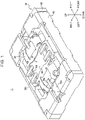
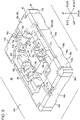
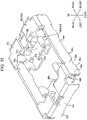
- Fig. 1 is an external top perspective view of a connector 1 according to one embodiment in a state in which a first connector 10 and a second connector 50 are connected to each other.
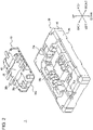
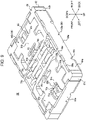
- Fig. 2 is an external top perspective view of the connector 1 according to one embodiment in a state in which the first connector 10 and the second connector 50 are separated from each other.
- the connector 1 includes the first connector 10 and the second connector 50 that can be connected to each other.
- the first connector 10 includes a first insulator 20, and a first contacts 30a that includes a first contacting portion 34a described below and that is attached to the first insulator 20.
- the first connector 10 includes a signal contact 30b and a first shield member 40 that are attached to the first insulator 20.
- the second connector 50 includes a second insulator 60 that is fittable to the first insulator 20.
- the second connector 50 includes a second contact 70a that includes a second contacting portion 74a (described below) and that is attached to the second insulator 60, the second contacting portion 74a being in contact with the first contacting portion 34a in a fitted state in which the first insulator 20 and the second insulator 60 are fitted to each other.
- the second connector 50 includes a signal contact 70b and a second shield member 80 that are attached to the second insulator 60.
- a shield member of the connector 1 is attached to the first insulator 20 and the second insulator 60.
- the shield member includes the first shield member 40 attached to the first insulator 20 and the second shield member 80 attached to the second insulator 60.
- the second connector 50 is a receptacle connector.
- the first connector 10 is a plug connector.
- the second connector 50 in which the second contact 70a and the signal contact 70b are elastically deformed in the fitted state in which the first insulator 20 and the second insulator 60 are fitted to each other, is a receptacle connector.
- the first connector 10 in which the first contact 30a and the signal contact 30b do not elastically deform, is a plug connector.
- the types of the first connector 10 and the second connector 50 are not limited to these.
- the second connector 50 may serve as a plug connector
- the first connector 10 may serve as a receptacle connector.
- the first connector 10 and the second connector 50 are to be mounted respectively on the circuit boards CB1 and CB2.
- the first connector 10 and the second connector 50 electrically connect the circuit board CB1 and the circuit board CB2.
- the circuit boards CB1 and CB2 may be rigid boards, or may be any circuit boards other than rigid boards.
- at least one of the circuit boards CB1 and CB2 may be a flexible printed circuit board.
- first connector 10 and the second connector 50 are connected to each other in a direction that is perpendicular to the circuit boards CB1 and CB2.
- the first connector 10 and the second connector 50 are connected to each other, for example, along the up-down direction.
- the connection method is not limited to this.
- the first connector 10 and the second connector 50 may be connected to each other in a direction parallel to the circuit boards CB1 and CB2.
- the first connector 10 and the second connector 50 may be connected to each other so that one of these is perpendicular to a circuit board to which the one is mounted and the other is parallel to a circuit board to which the other is mounted.
- the “fitting direction” described in the claims corresponds to, for example, the up-down direction in the present specification.
- first direction being perpendicular to a fitting direction corresponds to, for example, the left-right direction.
- longitudinal direction of the connector 1 corresponds to, for example, the left-right direction.
- second direction being perpendicular to first direction and the fitting direction corresponds to, for example, the front-back direction.
- transversal direction of the connector 1 corresponds to, for example, the front-back direction.
- the “circuit board side in the fitting direction” corresponds to, for example, the lower side.
- the connector 1 includes two pairs of the first contacts 30a and the second contacts 70a that are in contact with each other in a state in which the first connector 10 and the second connector 50 are connected.
- the connector 1 has a shield structure that shields each pair of the first contact 30a and the second contacts 70a that are in contact with each other in a fitted state in which the first insulator 20 and the second insulator 60 are fitted to each other.
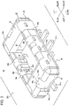
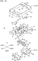
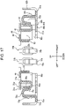
- Fig. 3 is an external top perspective view illustrating only the first connector 10 of Fig. 1 .
- Fig. 4 is a bottom perspective view illustrating only the first connector 10 of Fig. 1 .
- the first connector 10 is obtained, for example, by integrally insert-molding the first contact 30a, the signal contact 30b. the first shield member 40, and the first insulator 20.
- the first insulator 20 of the first connector 10 is made of an insulating and heat-resistant synthetic resin material.
- the first insulator 20 extends in a plate-like shape in the left-right direction.
- the first insulator 20 includes a bottom plate portion 21 forming a lower part thereof and a ring-shaped outer peripheral wall 22 protruding upward from the entire peripheral edge part of an upper surface of the bottom plate portion 21.
- the outer peripheral wall 22 includes a pair of transversal walls 22a that extend in the front-back direction and a pair of longitudinal walls 22b that extend in the left-right direction.
- the first insulator 20 includes a fitting recess 23 defined by a space formed by the bottom plate portion 21 and the outer peripheral wall 22.
- the first insulator 20 has a first-contact holding groove 24a formed from an outer surface in the left-right direction of the transversal wall 22a of the outer peripheral wall 22 to the inside of the transversal wall 22a.
- the first-contact holding groove 24a integrally holds the first contact 30a.
- the first insulator 20 has a signal-contact holding groove 24b formed from an outer surface to an inner surface in the front-back direction of the longitudinal wall 22b of the outer peripheral wall 22.
- the signal-contact holding groove 24b integrally holds the signal contact 30b.
- the first insulator 20 has a first-shield-member holding groove 25 formed from an outer surface and an inner surface in the left-right direction to an outer surface in the front-back direction of the transversal wall 22a of the outer peripheral wall 22.
- the first-shield-member holding groove 25 integrally holds the first shield member 40.
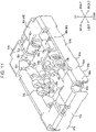
- Fig. 5 is a top perspective view of the first connector 10 of Fig. 3 in a state in which only the first insulator 20 is not illustrated.
- Fig. 6 is a top perspective view illustrating only a pair of the first shield members 40 of Fig. 5 .
- Fig. 7 is a top perspective view illustrating only a pair of the first contacts 30a of Fig. 5 . Referring mainly to Figs. 5 to 7 , the configuration of each of the first contact 30a, the signal contact 30b, and the first shield member 40 will be described in detail.
- the first contact 30a is made by, for example, forming a thin plate of: a copper alloy, including phosphor bronze, beryllium copper, or titanium copper; or a Corson copper alloy into the shape illustrated in Figs. 5 and 7 by using a progressive die (stamping).
- the surface of the first contact 30a is plated by gold, tin, or the like after forming a sublayer by nickel plating.
- the first contact 30a includes a mount portion 31a that extends outward in an L-shape.
- the first contact 30a includes a connection portion 32a that is formed upward in a reversely tapered shape from an upper end part of the mount portion 31a.
- the first contact 30a includes a curved portion 33a that extends in a U-shape upward from the connection portion 32a.
- the first contact 30a includes the first contacting portion 34a that is configured to include an outer surface in the left-right direction on the free-end side of the curved portion 33a.
- the first contact 30a is held with respect to the first-contact holding groove 24a, because the entirety of the first contact 30a excluding the mount portion 31a is integrated with the first-contact holding groove 24a.
- the first contact 30a is disposed along the transversal direction of the connector 1.
- the signal contact 30b is made by, for example, forming a thin plate of: a copper alloy, including phosphor bronze, beryllium copper, or titanium copper; or a Corson copper alloy into the shape illustrated in Fig. 5 by using a progressive die (stamping).
- the surface of the signal contact 30b is plated by gold, tin, or the like after forming a sublayer by nickel plating.
- the signal contact 30b includes a mount portion 31b that extends outward in an L-shape.
- the signal contact 30b includes a contacting portion 32b that extends upward from an upper end part of the mount portion 31b.
- the contacting portion 32b has a contact surface formed of an inner surface in the front-back direction.
- the contacting portion 32b is formed wider than the mount portion 31b in the left-right direction.
- the signal contact 30b includes a curved portion 33b that extends in a U-shape outward from the contacting portion 32b.
- the signal contact 30b includes a contacting portion 34b that is configured to include an outer surface in the left-right direction on the free-end side of the curved portion 33b.
- the signal contact 30b includes a projection 35b formed on an upper part of the contact surface of the contacting portion 32b.
- the free end of the curved portion 33b is formed at approximately the same height position as the contacting portion 32b.
- the signal contact 30b is integrally held with respect to the signal-contact holding groove 24b, because the entirety of the signal contact 30b excluding the mount portion 31b is in surface-contact with the signal-contact holding groove 24b.
- the tip of the mount portion 31b of the signal contact 30b is positioned outside of the longitudinal wall 22b.
- the first shield member 40 is made by forming a thin plate of any appropriate metal material into the shape illustrated in Figs. 5 and 6 by using a progressive die (stamping).
- the method of forming the first shield member 40 includes a step of bending the thin plate in the plate-thickness direction after punching the thin plate.
- the first shield member 40 is integrally held with respect to the first-shield-member holding groove 25 of the first insulator 20, and is disposed on each of the left and right sides of the first insulator 20.
- the first shield member 40 includes a first base portion 41 that forms a lower end part thereof.
- the first shield member 40 includes a first extending portion 42 that extends in an L-shape along the up-down direction from the first base portion 41 and that is disposed on each of two sides of the first base portion 41 in the front-back direction.
- the first shield member 40 includes a second extending portion 43 that extends in a U-shape along the up-down direction from each of a pair of edges, along the left-right direction, of the first base portion 41.
- the first shield member 40 includes, at an inner end part thereof in the left-right direction, a coupling portion 44 that couples the first base portions 41 on the front and back sides.
- the first shield member 40 includes a first shield portion 45 that extends in an L-shape along the up-down direction from the coupling portion 44 and that extends over the entire width of the coupling portion 44 in the front-back direction.
- the first shield member 40 includes a mount portion 46 formed of a lower surface of the first base portion 41 on each of the front and back sides.
- the mount portion 46 which is disposed on each of the front and back sides of one first shield member 40, is mounted, for example, in a separated state on a pair of ground patterns that are separated from each other on the mount surface the circuit board CB1.
- the mount portion 31a of the first contact 30a is soldered to a circuit pattern formed on the mount surface of the circuit board CB1.
- the mount portion 31b of the signal contact 30b is soldered to a circuit pattern formed on the mount surface.
- the mount portion 46 of the first shield member 40 is soldered to a circuit pattern formed on the mount surface.
- the first connector 10 is mounted on the circuit board CB1.
- electronic components other than the first connector 10, such as a communication module are mounted on the mount surface of the circuit board CB1.
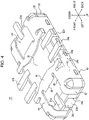
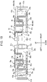
- Fig. 8 is an external top perspective view illustrating only the second connector 50 of Fig. 1 .
- Fig. 9 is a bottom perspective view illustrating only the second connector 50 of Fig. 1 .
- Fig. 10 is an exploded top perspective view of the second connector 50 of Fig. 8 .
- the second connector 50 is assembled, for example, by using the following method.
- the second contact 70a is press-fitted into the second insulator 60 from above.
- the signal contact 70b is press-fitted into the second insulator 60 from below.
- the second shield member 80 is press-fitted into the second insulator 60 from above and below.
- the second insulator 60 is a plate-shaped member that is formed by injection-molding an insulating and heat-resistant synthetic resin material and that extends in the left-right direction.
- the second insulator 60 includes a bottom plate portion 61 forming a lower part thereof and a ring-shaped outer peripheral wall 62 protruding upward while surrounding the entirety of the peripheral edge part of the bottom plate portion 61.
- the outer peripheral wall 62 includes a pair of transversal walls 62a that extend in the front-back direction and a pair of longitudinal walls 62b that extend in the left-right direction.
- the second insulator 60 includes a fitting raised portion 63 protruding upward from a central part of the bottom plate portion 61.
- the second insulator 60 has a second-contact holding groove 64a formed in a central part of the transversal wall 62a of the outer peripheral wall 62 in the front-back direction.
- the second-contact holding groove 64a holds the second contact 70a pressed thereinto.
- the second insulator 60 has a signal-contact holding groove 64b formed from an inner surface in the front-back direction of the longitudinal wall 62b of the outer peripheral wall 62 to an outer surface in the front-back direction of the fitting raised portion 63.
- the signal-contact holding groove 64b holds the signal contact 70b pressed thereinto.
- the second insulator 60 has a second-shield-member holding groove 65 formed from an outer surface in the left-right direction of the transversal wall 62a of the outer peripheral wall 62 to an outer surface in the front-back direction of the transversal wall 62a and inside of the transversal wall 62a.
- the second-shield-member holding groove 65 holds the second shield member 80 pressed thereinto.
- Fig. 11 is a top perspective view of the second connector 50 of Fig. 8 in a state in which only the second insulator 60 is not illustrated.
- Fig. 12 is a top perspective view illustrating only the second shield member 80 of Fig. 11 .
- Fig. 13 is a top perspective view illustrating only a pair of the second contacts 70a of Fig. 11 . Referring mainly to Figs. 11 to 13 , the configuration of each of the second contact 70a, the signal contact 70b, and the second shield member 80 will be described in detail.
- the second contact 70a is made by, for example, forming a thin plate of: a copper alloy, including phosphor bronze, beryllium copper, or titanium copper; or a Corson copper alloy into the shape illustrated in Figs. 11 and 13 by using a progressive die (stamping).
- the surface of the second contact 70a is plated by gold, tin, or the like after forming a sublayer by nickel plating.
- the second contact 70a includes a mount portion 71a that extends outward in an L-shape.
- the second contact 70a includes a latch portion 72a formed continuously from an upper end part of the mount portion 71a.
- the latch portion 72a is formed wider in the front-back direction than the mount portion 71a and a curved portion 73a described below.
- the second contact 70a includes the curved portion 73a that extends in a U-shape upward from the latch portion 72a.
- the second contact 70a includes the second contacting portion 74a configured to include an inner surface in the left-right direction on the free-end side of the curved portion 73a.
- the second contacting portion 74a has spring elasticity so that the second contacting portion 74a can elastically deform along the left-right direction.
- the second contact 70a is held with respect to the second-contact holding groove 64a, because the latch portion 72a is latched to the second-contact holding groove 64a.
- the second contact 70a is disposed along the transversal direction of the connector 1.
- the tip of the mount portion 71a of the second contact 70a is positioned inside of the outermost end in the left-right direction of the transversal wall 62a.
- the signal contact 70b is made by, for example, forming a thin plate of: a copper alloy having spring elasticity, including phosphor bronze, beryllium copper, or titanium copper; or a Corson copper alloy into the shape illustrated in Figs. 10 and 11 by using a progressive die (stamping).
- the surface of the signal contact 70b is plated by gold, tin, or the like after forming a sublayer by nickel plating.
- the signal contact 70b includes a mount portion 71b that extends outward in an L-shape.
- the signal contact 70b includes a pair of latch portions 72b including a portion that is formed upward continuously from an upper end part of the mount portion 71b and another portion that is separated from the portion in the front-back direction and that faces the portion.
- the latch portions 72b are formed wider than the mount portion 71b and a curved portion 73b described below in the left-right direction.
- the signal contact 70b includes the curved portion 73b that connects the pair of the latch portions 72b, an elastic contacting portion 74b that is S-shaped and that is continuous with the latch portion 72b formed inside, and a contacting portion 75b formed at a tip part of the elastic contacting portion 74b so as to face outward.
- the signal contact 70b includes a contacting portion 76b including a projection that projects from an inner surface in the front-back direction of the curved portion 73b.
- the free end of the elastic contacting portion 74b is formed at approximately the same height position as the contacting portion 75b.
- the signal contact 70b is held with respect to the signal-contact holding groove 64b, because the latch portion 72b is latched to the signal-contact holding groove 64b.
- the elastic contacting portion 74b can elastically deform in the front-back direction in the signal-contact holding groove 64b formed in the fitting raised portion 63.
- the tip of the mount portion 71b of the signal contact 70b is positioned inside of the outermost end in the front-back direction of the longitudinal wall 62b.
- the second shield member 80 is made by forming a thin plate of any appropriate metal material into the shape illustrated in Figs. 10 to 12 by using a progressive die (stamping).
- the method of forming the second shield member 80 includes a step of bending the thin plate in the plate-thickness direction after punching the thin plate.
- the second shield member 80 is held by the second insulator 60 by being press-fitted into the second-shield-member holding groove 65 of the second insulator 60.
- the second shield member 80 includes, for example, three members. To be more specific, the second shield member 80 includes a first member 80a that is attached to the second insulator 60 from above so as to surround the outer peripheral wall 62 from four sides. The second shield member 80 includes a pair of second members 80b that are attached to the second insulator 60 from below so as to be disposed on the left and right sides of the second insulator 60.
- the second member 80b includes a second base portion 81b forming a lower end part thereof.
- the second base portion 81b is adjacent to the second contact 70a in the left-right direction.
- the second member 80b includes a second shield portion 82b that extends in an L-shape along the up-down direction from the second base portion 81b and that extends over the entire width of the second base portion 81b in the front-back direction.
- the second member 80b includes a third shield portion 83b that forms a central part of the second base portion 81b and that extends over the entire width of the second base portion 81b in the front-back direction.
- the second member 80b includes a latch portion 84b that extends in an L-shape along the up-down direction from each of a pair of edges, along the left-right direction, of the second base portion 81b.
- the second member 80b includes a contacting portion 85b that is disposed inside of the latch portion 84b in the left-right direction and that extends in an S-shape along the up-down direction from each of a pair of edges, along the left-right direction, of the second base portion 81b.
- the contacting portion 85b is formed at an inner end part of the second member 80b in the left-right direction.
- the second member 80b includes a first mount portion 86b that is disposed inside of the second contact 70a in the left-right direction and that is to be mounted on the circuit board CB2.
- the first mount portion 86b is formed in an L-shape on a side of the second base portion 81b opposite to the second contact 70a in the left-right direction.
- the first mount portion 86b is formed at an inner end part of the second member 80b in the left-right direction.
- a pair of the first mount portions 86b are disposed respectively on the front and back sides of the second base portion 81b in the second member 80b.
- the first mount portions 86b are symmetrically disposed on both sides with respect to the second contact 70a in the front-back direction.
- the pair of first mount portions 86b are respectively mounted, for example, in a separated state on a pair of circuit patterns that are separated from each other on the mount surface of the circuit board CB2.
- the second member 80b includes a second mount portion 87b that is formed by a lower surface on each of the front and back sides of an outer end part of the second base portion 81b in the left-right direction and a lower surface of the latch portions 84b on each of the front and back sides.
- the second mount portion 87b disposed on the front side and the second mount portion 87b disposed on the back side of one second member 80b are respectively mounted, for example, on a pair of circuit patterns that are separated from each other on the mount surface of the circuit board CB2.
- the contacting portion 85b extends upward from the first mount portion 86b.
- the contacting portion 85b extends from an end part, outside in the front-back direction, of the first mount portion 86b.
- the contacting portion 85b extends in an S-shape from the first mount portion 86b and has spring elasticity.
- the contacting portion 85b extends along the left-right direction between the first mount portion 86b and the second contact 70a.
- the width of the contacting portion 85b in the left-right direction is greater than or equal to the mount width of the first mount portion 86b in the left-right direction.
- the contacting portion 85b is symmetrically disposed on each of two sides with respect to the second contact 70a in the front-back direction.
- the second member 80b is held with respect to the second-shield-member holding groove 65, because the latch portion 84b and the second shield portion 82b are latched to the second-shield-member holding groove 65.
- the pair of latch portions 84b are latched to grooves of the second-shield-member holding groove 65 that are formed inside of the front and back sides of the transversal wall 62a.
- the second shield portion 82b is latched to a groove of the second-shield-member holding groove 65 that is formed in an outer surface in the left-right direction of the transversal wall 62a.
- the first member 80a includes a third base portion 81a that forms an upper end part thereof.
- the first member 80a includes, a fourth shield portion 82a that extends in the left-right direction with a predetermined width in an outer peripheral part thereof in the front-back direction.
- the first member 80a includes a fifth shield portion 83a that is disposed further outside than the second shield portion 82b in the left-right direction.
- the fifth shield portion 83a has a larger width in the front-back direction than the second shield portion 82b, and is disposed so as to overlap the entirety of the second shield portion 82b in the front-back direction. As illustrated also in Fig.
- the first member 80a includes an outer-peripheral-side shield portion 84a that is disposed outside of the longitudinal wall 62b of the second insulator 60 along the left-right direction.
- the outer-peripheral-side shield portion 84a extends along the left-right direction so as to couple the fourth shield portions 82a positioned on the left and right sides.
- the first member 80a includes a contacting portion 85a that extends along the up-down direction from the third base portion 81a and that is disposed on each of two sides with respect to the second contact 70a in the front-back direction.
- the contacting portion 85a has spring elasticity so that the contacting portion 85a can elastically deform along the left-right direction.
- the first member 80a includes a latch portion 86a that is formed at each of two end parts, in the left-right direction, of an outer peripheral part thereof in the front-back direction.
- the first member 80a includes a first mount portion 87a that extends linearly downward from a lower end part on each of the front and back sides of the fifth shield portion 83a.
- the first member 80a includes a second mount portion 88a that extends linearly downward from a lower end part of the latch portion 86a.
- the first member 80a includes a third mount portion 89a that extends linearly downward from each of the left and right end parts of the outer-peripheral-side shield portion 84a.
- the first mount portion 87a on the front side in the left direction and the second mount portion 88a on the left side in the front direction that are adjacent to each other are mounted on the same ground pattern on the mount surface of the circuit board CB2.
- first mount portion 87a on the back side in the left direction and the second mount portion 88a on the left side in the back direction that are adjacent to each other are mounted on the same ground pattern on the mount surface of the circuit board CB2.
- the right side of the first member 80a is configured in the same way.
- four third mount portions 89a are respectively mounted, in a separated state, on four ground patterns that are separated from each other on the mount surface of the circuit board CB2.
- the first member 80a is held with respect to the second-shield-member holding groove 65, because the latch portion 86a is latched to the second-shield-member holding groove 65.
- the mount portion 71a of the second contact 70a is soldered to a circuit pattern formed on the mount surface of the circuit board CB2.
- the mount portion 71b of the signal contact 70b is soldered to a circuit pattern formed on the mount surface.
- the first mount portion 87a, the second mount portion 88a, and the third mount portion 89a of the first member 80a of the second shield member 80; and the first mount portion 86b and the second mount portion 87b of the second member 80b are soldered to a ground pattern formed on the mount surface.
- the first mount portion 87a on the front side in the left direction and the second mount portion 88a on the left side in the front direction of the first member 80a; and the second mount portion 87b on the front side of the second member 80b that is disposed on the left side are soldered to the same ground pattern.
- the first member 80a and the second member 80b electrically as one shield member.
- the second connector 50 is mounted on the circuit board CB2.
- electronic components other than the second connector 50 such as a central processing unit (CPU), a controller, and a memory, are mounted on the mount surface of the circuit board CB2.
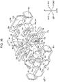
- Fig. 14 is a top perspective view of the connector 1 of Fig. 1 in a state in which only the first insulator 20 and the second insulator 60 are not illustrated.
- Fig. 15 is a sectional view taken along an arrow XV-XV of Fig. 14 . Referring to Figs. 14 and 15 , the configuration of the connector 1 in a fitted state in which the first connector 10 and the second connector 50 are connected and the first insulator 20 and the second insulator 60 are fitted to each other will be described.
- the first connector 10 and the second connector 50 are caused to face each other in the up-down direction while causing the front-back positions and the left-right positions thereof to approximately coincide with each other.
- the first connector 10 is moved downward.
- the first connector 10 and the second connector 50 are connected to each other, and the fitted state of the connector 1 can be obtained.
- the fitting recess 23 of the first insulator 20 and the fitting raised portion 63 of the second insulator 60 are fitted to each other.
- the first contacting portion 34a of the first contact 30a and the second contacting portion 74a of the second contact 70a are in contact with each other, and the second contacting portion 74a, which has spring elasticity, is elastically deformed outward in the left-right direction.
- the first contact 30a and the second contact 70a are in contact with each other at only one point due to the first contacting portion 34a and the second contacting portion 74a.
- the projection 35b of the signal contact 30b has moved over the contacting portion 75b of the signal contact 70b while moving downward, and the contacting portion 32b of the signal contact 30b and the contacting portion 75b of the signal contact 70b are in contact with each other.
- the elastic contacting portion 74b which has spring elasticity, is elastically deformed inward in the front-back direction.
- the contacting portion 34b of the signal contact 30b and the contacting portion 76b of the signal contact 70b are in contact with each other.
- the signal contact 30b and the signal contact 70b are in contact with each other at two points due to the contacting portion 32b and the contacting portion 75b and due to the contacting portion 34b and the contacting portion 76b.
- the first extending portion 42 of the first shield member 40 and the contacting portion 85a of the first member 80a of the second shield member 80 are in contact with each other.
- the first extending portion 42 of the first shield member 40 extends along the up-down direction from the first base portion 41, and is disposed on each of two sides, in the front-back direction, with respect to the contact part between the first contact 30a and the second contact 70a.
- the first extending portion 42 of the first shield member 40 is disposed adjacent to the first contacting portion 34a and the second contacting portion 74a, which are in contact with each other, on each of two sides in the front-back direction.
- the contacting portion 85a of the first member 80a extends along the up-down direction from the third base portion 81a, which is disposed on the same side as the first base portion 41 in the up-down direction, and is disposed on each of two sides, in the front-back direction, with respect to the contact part between the first contact 30a and the second contact 70a.
- the contacting portion 85a of the first member 80a is disposed so as to be adjacent to the first contacting portion 34a and the second contacting portion 74a, which are in contact with each other, on each of two sides in the front-back direction.
- the first shield member 40 and the first member 80a are in contact with each other at two points due to two pairs of the first extending portions 42 and the contacting portions 85a that sandwich the first contacting portion 34a and the second contacting portion 74a in the front-back direction while being adjacent thereto.
- the two pairs of first extending portions 42 and contacting portions 85a are symmetrically disposed on both sides, in the front-back direction, with respect to the contact part between the first contact 30a and the second contact 70a.
- the second extending portion 43 of the first shield member 40 and the contacting portion 85b of the second member 80b of the second shield member 80 are in contact with each other.
- the second extending portion 43 of the first shield member 40 extends along the up-down direction from the first base portion 41, and is disposed on each of two sides, in the front-back direction, with respect to the contact part between the first contact 30a and the second contact 70a.
- the second extending portion 43 of the first shield member 40 is disposed in proximity to the first contacting portion 34a and the second contacting portion 74a, which are in contact with each other, on each of two sides in the front-back direction.
- the contacting portion 85b of the second member 80b extends along the up-down direction from the second base portion 81b, which is disposed on a side opposite to the first base portion 41 in the up-down direction, and is disposed on each of two sides, in the front-back direction, with respect to the contact part between the first contact 30a and the second contact 70a.
- the contacting portion 85b of the second member 80b is disposed so as to be in proximity to the first contacting portion 34a and the second contacting portion 74a, which are in contact with each other, on each of two sides in the front-back direction.
- the first shield member 40 and the second member 80b are in contact with each other at two points due to two pairs of the second extending portions 43 and the contacting portions 85b that sandwich the first contacting portion 34a and the second contacting portion 74a, which are in contact with each other, while being in proximity thereto.
- the two pairs of second extending portions 43 and contacting portions 85b are symmetrically disposed on both sides, in the front-back direction, with respect to the contact part between the first contact 30a and the second contact 70a.
- the first shield member 40 and the second shield member 80 are in contact with each other at four points that are adjacent to or in proximity to the first contacting portion 34a and the second contacting portion 74a, which are in contact with each other.
- the first shield portion 45 of the first shield member 40 is disposed inside in the left-right direction of the first contacting portion 34a and the second contacting portion 74a, which are in contact with each other.
- the second shield portion 82b of the second member 80b of the second shield member 80 is disposed outside in the left-right direction of the first contacting portion 34a and the second contacting portion 74a, which are in contact with each other.
- the first contacting portion 34a and the second contacting portion 74a which are in contact with each other, are shielded by the first shield portion 45 and the second shield portion 82b from both sides in the left-right direction.
- the third shield portion 83b of the second member 80b of the second shield member 80 is disposed on a side opposite to the fitting side in the up-down direction of the first contacting portion 34a and the second contacting portion 74a, which are in contact with each other. In this way, the first contacting portion 34a and the second contacting portion 74a, which are in contact with each other, are shielded by the third shield portion 83b from the side opposite to the fitting side.
- the fourth shield portion 82a of the first member 80a of the second shield member 80 is disposed on each of two sides, in the front-back direction, with respect to the first contacting portion 34a and the second contacting portion 74a, which are in contact with each other. In this way, the first contacting portion 34a and the second contacting portion 74a, which are in contact with each other, are shielded by the fourth shield portion 82a from each of two sides in the front-back direction.
- the fifth shield portion 83a of the first member 80a of the second shield member 80 is disposed further outside than the second shield portion 82b in the left-right direction.
- the first contacting portion 34a and the second contacting portion 74a which are in contact with each other, are shielded by the double structure of the second shield portion 82b and the fifth shield portion 83a outside in the left-right direction.
- the first shield portion 45 and the second shield portion 82b shield the first contacting portion 34a and the second contacting portion 74a, which are in contact with each other, from both sides in the left-right direction, and the third shield portion 83b shields the first contacting portion 34a and the second contacting portion 74a from the side opposite to the fitting side.
- the first contacting portion 34a and the second contacting portion 74a which are in contact with each other, are shielded from at least three directions.
- the third shield portion 83b shields the first contacting portion 34a and the second contacting portion 74a, which are in contact with each other, from the side opposite to the fitting side, the noise shielding effect between the first contact 30a and the second contact 70a and the circuit board CB2 is improved.
- inflow of noise from the circuit board CB2 to the first contact 30a and the second contact 70a and outflow of noise from the first contact 30a and the second contact 70a to the circuit board CB2 are effectively suppressed.
- the shield member includes the first shield member 40 attached to the first insulator 20 and the second shield member 80 attached to the second insulator 60.
- the first shield portion 45 is formed in the first shield member 40
- the second shield portion 82b and the third shield portion 83b are formed in the second shield member 80.
- these shield portions are integrally formed in one of the first shield member 40 and the second shield member 80, the shapes of the first shield member 40 and the second shield member 80 are simplified.
- the third shield portion 83b corresponding to the lower surface of the shield portion and the second shield portion 82b corresponding to the left surface of the shield portion so as to be integrated with the second member 80b of the second shield member 80, it is possible to eliminate a gap between the lower surface and the left surface and, at the same time, to establish a reliable electrical connection between the third shield portion 83b and the second shield portion 82b. Accordingly, a higher noise shielding effect can be obtained.
- the second shield member 80 includes the fourth shield portion 82a that is disposed on each of two sides, in the front-back direction, with respect to the first contacting portion 34a and the second contacting portion 74a, which are in contact with each other.
- the shield member includes five shield portions, together with the first shield portion 45, the second shield portion 82b, the third shield portion 83b.
- the first contacting portion 34a and the second contacting portion 74a which are in contact with each other, are shielded from five directions. Accordingly, inflow of noise to the first contact 30a and the second contact 70a from the outside and outflow of noise from the first contact 30a and the second contact 70a to the outside are more effectively suppressed. As a result, for example, also in high-speed transmission, it is possible to obtain better transmission characteristics for high-frequency signals.
- the second shield member 80 includes the fifth shield portion 83a that is disposed further outside than the second shield portion 82b in the left-right direction.
- the second shield member 80 has a double structure of the second shield portion 82b and the fifth shield portion 83a outside in the left-right direction of the first contacting portion 34a and the second contacting portion 74a, which are in contact with each other.
- the noise shielding effect particularly from the left-right direction is improved, and inflow of noise to the first contact 30a and the second contact 70a from the outside and outflow of noise from the first contact 30a and the second contact 70a to the outside are more effectively suppressed.
- Inflow of noise from above can be suppressed by superposing the fifth shield portion 83a of the first member 80a on the second shield portion 82b of the second member 80b.
- the fifth shield portion 83a of the first member 80a on the second shield portion 82b of the second member 80b.
- the second shield member 80 includes the outer-peripheral-side shield portion 84a, which is disposed outside of the second insulator 60 along the left-right direction.
- the second shield member 80 has a shield portion for the signal contact 30b and the signal contact 70b, which are in contact with each other, outside in the front-back direction.
- the noise shielding effect is improved also for the signal contact 30b and the signal contact 70b.
- inflow of noise to the signal contact 30b and the signal contact 70b from the outside and outflow of noise from the signal contact 30b and the signal contact 70b to the outside are effectively suppressed.
- the pair of first contacts 30a are disposed along the transversal direction of the connector 1 at both ends of the first insulator 20 in the left-right direction.
- the pair of second contacts 70a are disposed along the transversal direction of the connector 1 at both ends of the second insulator 60 in the left-right direction.
- the connector 1 includes the plurality of signal contacts 30b and the signal contacts 70b that differ from the first contacts 30a and the second contacts 70a, it is possible for the connector 1 to transmit various signals between the circuit board CB1 and the circuit board CB2. Because the plurality of signal contacts 30b and the signal contacts 70b are disposed along the longitudinal direction of the connector 1, the signal contacts 30b and the signal contacts 70b are separated far from the first contacts 30a and the second contacts 70a, which are disposed along the transversal direction of the connector 1. It is possible to separate the signal contacts 30b and the signal contacts 70b far from the first contacts 30a and the second contacts 70a in the connector 1. Accordingly, it is possible to shield the signal contacts 30b and the signal contacts 70b by using shield members that are independent from each other. At this time, it is possible to perform shielding from multiple directions, because a sufficient space for providing the shield members can be obtained.
- the shape, the disposition, the orientation, and the number of each element described above are not limited to those in the forgoing descriptions and drawings.
- the shape, the disposition, the orientation, and the number of each element may be determined in any appropriate way as long as the function thereof can be realized.
- a method of assembling the first connector 10 and the second connector 50 described above is not limited to what has been described above.
- a method of assembling the first connector 10 and the second connector 50 may be any method as long as the method allows assembly so that the functions of each of these can be fully exploited.
- at least one of the first contact 30a, the signal contact 30b, and the first shield member 40 may be attached to the first insulator 20 not by insert molding but by press-fitting.
- at least one of the second contact 70a, the signal contact 70b, and the second shield member 80 may be integrally formed with the second insulator 60 not by press-fitting but by insert molding.
- the shield member includes the first shield member 40 and the second shield member 80.
- the configuration of the shield member is not limited to this.
- the shield member may be integrally formed and may be attached to at least one of the first insulator 20 and the second insulator 60 that are in the fitted state.
- each of the shield portions including the fourth shield portion 82a, the fifth shield portion 83a, and the outer-peripheral-side shield portion 84a may be formed in either one of the first shield member 40 and the second shield member 80.
- all shield portions may be formed in only the second shield member 80.
- Each shield portion may be formed in a state in which the shield portion is divided between the first shield member 40 and the second shield member 80.
- the third shield portion 83b is disposed directly below the first contacting portion 34a and the second contacting portion 74a, which are in contact with each other, as illustrated in Fig. 15 and other figures.
- the third shield portion 83b may be disposed at a position that is displaced in the left-right direction with respect to the first contacting portion 34a and the second contacting portion 74a, which are in contact with each other.
- the second shield member 80 includes the fourth shield portion 82a that is disposed on each of two sides with respect to the first contacting portion 34a and the second contacting portion 74a, which are in contact with each other.
- the second shield member 80 may have the fourth shield portion 82a only on one side or need not have the fourth shield portion 82a, as long as a good noise shielding effect can be obtained.
- Fig. 16 is a perspective view, corresponding to Fig. 14 , of a modification of the connector 1 of Fig. 1 in a state in which only the first insulator 20 and the second insulator 60 are not illustrated.
- Fig. 17 is a sectional view taken along an arrow XVII-XVII of Fig. 16 .
- the second shield member 80 has only the second member 80b without having the first member 80a.
- the second shield member 80 includes the fifth shield portion 83a.
- the second shield member 80 need not include the fifth shield portion 83a as long as a good noise shielding effect can be obtained.
- the second shield member 80 has the outer-peripheral-side shield portion 84a.
- the second shield member 80 need not have the outer-peripheral-side shield portion 84a, as long as a good noise shielding effect can be obtained.
- the shield member includes the first shield portion 45, the second shield portion 82b, the third shield portion 83b, the fourth shield portion 82a, and the fifth shield portion 83a.
- the shield member may include, in addition to the first shield portion 45 to the fifth shield portion 83a, a sixth shield portion that is disposed on a side opposite to the third shield portion 83b in the up-down direction with respect to the first contacting portion 34a and the second contacting portion 74a, which are in contact with each other.
- the sixth shield portion may be formed in either one of the first shield member 40 and the second shield member 80.
- the sixth shield portion shields the first contacting portion 34a and the second contacting portion 74a, which are in contact with each other, from above. Accordingly, the noise shielding effect is further improved, because the first shield portion 45 to the fifth shield portion 83a and the sixth shield portion shield the first contacting portion 34a and the second contacting portion 74a, which are in contact with each other, from six directions, which are the front-back, left-right, and up-down directions.
- the first extending portion 42 of the first shield member 40 and the contacting portion 85a of the second shield member 80 are in contact with each other on each of two sides, in the front-back direction, with respect to the contact part between the first contact 30a and the second contact 70a.
- this is not a limitation.
- the second shield member 80 need not have the contacting portion 85a, and only the first extending portion 42 of the first shield member 40 may be formed on each of two sides with respect to the contact part between the first contact 30a and the second contact 70a.
- first base portion 41 and the first extending portion 42 are formed in the first shield member 40.
- each of constituent portions including the first base portion 41 and the first extending portion 42 may be formed in either one of the first shield member 40 and the second shield member 80.
- Each of the constituent portions may be formed in a state of being divided between the first shield member 40 and the second shield member 80.
- the two pairs of second extending portions 43 and contacting portions 85b are symmetrically disposed on both sides, in the front-back direction, with respect to the contact part between the first contact 30a and the second contact 70a.
- this is not a limitation.
- the two pairs of second extending portions 43 and contacting portions 85b may be asymmetrically disposed.
- the two pairs of first extending portions 42 and contacting portions 85a are symmetrically disposed on both sides, in the front-back direction, with respect to the contact part between the first contact 30a and the second contact 70a.
- this is not a limitation.
- the two pairs of first extending portions 42 and contacting portions 85a may be asymmetrically disposed.
- the contacting portion 85b of the second shield member 80 extends between the first mount portion 86b and the second contact 70a along the left-right direction.
- the contacting portion 85b of the second shield member 80 may extend along any direction.
- the width of the contacting portion 85b of the second shield member 80 in the left-right direction is greater than or equal to the mount width of the first mount portion 86b in the left-right direction.
- this is not a limitation.
- the width of the contacting portion 85b in the left-right direction may be smaller than the mount width of the first mount portion 86b in the left-right direction.
- the contacting portion 85b of the second shield member 80 extends in an S-shape from the first mount portion 86b.
- the contacting portion 85b may extend in any shape from the first mount portion 86b.
- the contacting portion 85b of the second shield member 80 has spring elasticity.
- the contacting portion 85b need not have spring elasticity.
- the second extending portion 43, which is in contact with the contacting portion 85b may have spring elasticity.
- first contact 30a and the second contact 70a are disposed along the transversal direction of the connector 1.
- the first contact 30a and the second contact 70a may be disposed along the longitudinal direction of the connector 1.
- the pair of first contacts 30a are disposed at both ends of the first insulator 20 in the left-right direction and the pair of second contacts 70a are disposed at both ends of the second insulator 60 in the left-right direction.
- the pair of first contacts 30a may be disposed inside of the first insulator 20 in the left-right direction
- the pair of second contacts 70a may be disposed inside of the second insulator 60 in the left-right direction.
- the connector 1 includes a plurality of contacts that differ from the first contact 30a and the second contact 70a, that is, the signal contact 30b and the signal contact 70b.
- the connector 1 need not have the signal contact 30b and the signal contact 70b.
- the plurality of contacts are disposed along the longitudinal direction of the connector 1. However, this is not a limitation.
- the plurality of contacts may be disposed along the transversal direction of the connector 1.
- the second shield member 80 includes the first member 80a and the second member 80b.
- the second shield member 80 may be integrally formed as a single member without being divided into two members.
- each mount portion in the above embodiment is not limited to what has been described above.
- Each mount portion may have any mount pattern formed on the mount surface of a corresponding circuit board.
- the connector 1 is mounted in an electronic apparatus including the circuit board CB1 and the circuit board CB2.
- the electronic apparatus include: any communication terminal device such as a smartphone; and any information processing machine such as a personal computer, a copier, a printer, a facsimile, and a multifunctional machine.
- examples of the electronic apparatus include any industrial equipment.
- Such an electronic apparatus can obtain a good noise shielding effect due to the connector 1.
- Such an electronic apparatus has good transmission characteristics in signal transmission. Accordingly, reliability of the electronic apparatus as a product is improved.
Abstract
Description
- The present application claims priority of
Japanese Patent Application No. 2019-235161, filed in Japan Patent Office on December 25, 2019 - The present disclosure relates to a connector and an electronic apparatus.
- In recent years, regarding electronic apparatuses, increase in communication speed and increase in information amount have considerably progressed. Since high frequency bands are used in communication systems in recent years, it is important not only to obtain good transmission characteristics but also to take measures against noises inside the electronic apparatuses. Thus, it is required for a connector incorporated in such an electronic apparatus to have a shield structure that can obtain a sufficient noise shielding effect.
-
PTL 1 discloses an electric connector device that enables reduction in size of a connector in the width direction in a structure in which a shield shell is disposed at a position outside of a contact member. - PTL 1:
Japanese Unexamined Patent Application Publication No. 2019-087382 - A connector according to one embodiment of the present disclosure,
which is a connector to be mounted on a circuit board, includes: - a first connector including a first insulator and a pair of first contacts each of which includes a first contacting portion and that are attached to the first insulator;
- a second connector including a second insulator that is fittable to the first insulator and a pair of second contacts each of which includes a second contacting portion and that are attached to the second insulator, the second contacting portion being in contact with the first contacting portion in a fitted state in which the first insulator and the second insulator are fitted to each other; and
- a shield member that is attached to the first insulator and the second insulator.
- The shield member includes
- a first shield portion and a second shield portion that are respectively disposed inside and outside in a first direction with respect to the first contacting portion and the second contacting portion that are in contact with each other in the fitted state, the first direction being perpendicular to a fitting direction in which the first insulator and the second insulator are fitted to each other, and
- a third shield portion that is disposed on the circuit board side in the fitting direction with respect to the first contacting portion and the second contacting portion that are in contact with each other in the fitted state.
- An electronic apparatus according to one embodiment of the present disclosure includes
the connector. -
- [
Fig. 1] Fig. 1 is an external top perspective view of a connector according to one embodiment in a state in which a first connector and a second connector are connected to each other. - [
Fig. 2] Fig. 2 is an external top perspective view of the connector according to one embodiment in a state in which the first connector and the second connector are separated from each other. - [
Fig. 3] Fig. 3 is an external top perspective view illustrating only the first connector ofFig. 1 . - [
Fig. 4] Fig. 4 is a bottom perspective view illustrating only the first connector ofFig. 1 . - [
Fig. 5] Fig. 5 is a top perspective view of the first connector ofFig. 3 in a state in which only a first insulator is not illustrated. - [
Fig. 6] Fig. 6 is a top perspective view illustrating only a pair of first shield members ofFig. 5 . - [
Fig. 7] Fig. 7 is a top perspective view illustrating only a pair of first contacts ofFig. 5 . - [
Fig. 8] Fig. 8 is an external top perspective view illustrating only the second connector ofFig. 1 . - [
Fig. 9] Fig. 9 is a bottom perspective view illustrating only the second connector ofFig. 1 . - [
Fig. 10] Fig. 10 is an exploded top perspective view of the second connector ofFig. 8 . - [
Fig. 11] Fig. 11 is a top perspective view of the second connector ofFig. 8 in a state in which only a second insulator is not illustrated. - [
Fig. 12] Fig. 12 is a top perspective view illustrating only the second shield member ofFig. 11 . - [
Fig. 13] Fig. 13 is a top perspective view illustrating only a pair of second contacts ofFig. 11 . - [
Fig. 14] Fig. 14 is a top perspective view of the connector ofFig. 1 in a state in which only the first insulator and the second insulator are not illustrated. - [
Fig. 15] Fig. 15 is a sectional view taken along an arrow XV-XV ofFig. 14 . - [
Fig. 16] Fig. 16 is a perspective view, corresponding toFig. 14 , of a modification of the connector ofFig. 1 in a state in which only the first insulator and the second insulator are not illustrated. - [
Fig. 17] Fig. 17 is a sectional view taken along an arrow XVII-XVII ofFig. 16 . - In the electric connector device described in
PTL 1, a shield structure with which a good noise shielding effect can be obtained for a pair of contacts that are in contact with each other in a connector in a fitted state is not sufficiently considered. - With a connector and an electronic apparatus according to one embodiment of the present disclosure, a good noise shielding effect can be obtained.
- Hereafter, one embodiment of the present disclosure will be described in detail with reference to the drawings. The front-back direction, the left-right direction, and the up-down direction in the following description are based on the directions of arrows in the figures. The directions of arrows in
Figs. 1 ,2 , and8 to 17 are consistent with each other between different figures. The directions of arrows inFigs. 3 to 7 are consistent with each other between different figures. In some figures, illustrations of circuit boards CB1 and CB2 (described below) are omitted for the purpose of simplicity of illustration. -
Fig. 1 is an external top perspective view of aconnector 1 according to one embodiment in a state in which afirst connector 10 and asecond connector 50 are connected to each other.Fig. 2 is an external top perspective view of theconnector 1 according to one embodiment in a state in which thefirst connector 10 and thesecond connector 50 are separated from each other. - For example, as illustrated in
Fig. 2 , theconnector 1 includes thefirst connector 10 and thesecond connector 50 that can be connected to each other. Thefirst connector 10 includes afirst insulator 20, and afirst contacts 30a that includes a first contactingportion 34a described below and that is attached to thefirst insulator 20. Thefirst connector 10 includes asignal contact 30b and afirst shield member 40 that are attached to thefirst insulator 20. - The
second connector 50 includes asecond insulator 60 that is fittable to thefirst insulator 20. Thesecond connector 50 includes asecond contact 70a that includes a second contactingportion 74a (described below) and that is attached to thesecond insulator 60, the second contactingportion 74a being in contact with the first contactingportion 34a in a fitted state in which thefirst insulator 20 and thesecond insulator 60 are fitted to each other. Thesecond connector 50 includes asignal contact 70b and asecond shield member 80 that are attached to thesecond insulator 60. - As described above, a shield member of the
connector 1 is attached to thefirst insulator 20 and thesecond insulator 60. To be more specific, the shield member includes thefirst shield member 40 attached to thefirst insulator 20 and thesecond shield member 80 attached to thesecond insulator 60. - In the following description, it is assumed that, for example, the
second connector 50 according to one embodiment is a receptacle connector. In the following description, it is assumed that thefirst connector 10 is a plug connector. In the following description, it is assumed that thesecond connector 50, in which thesecond contact 70a and thesignal contact 70b are elastically deformed in the fitted state in which thefirst insulator 20 and thesecond insulator 60 are fitted to each other, is a receptacle connector. In the following description, it is assumed that thefirst connector 10, in which thefirst contact 30a and thesignal contact 30b do not elastically deform, is a plug connector. The types of thefirst connector 10 and thesecond connector 50 are not limited to these. For example, thesecond connector 50 may serve as a plug connector, and thefirst connector 10 may serve as a receptacle connector. - In the following description, it is assumed that the
first connector 10 and thesecond connector 50 are to be mounted respectively on the circuit boards CB1 and CB2. In a state of being connected to each other, thefirst connector 10 and thesecond connector 50 electrically connect the circuit board CB1 and the circuit board CB2. The circuit boards CB1 and CB2 may be rigid boards, or may be any circuit boards other than rigid boards. For example, at least one of the circuit boards CB1 and CB2 may be a flexible printed circuit board. - In the following description, it is assumed that the
first connector 10 and thesecond connector 50 are connected to each other in a direction that is perpendicular to the circuit boards CB1 and CB2. Thefirst connector 10 and thesecond connector 50 are connected to each other, for example, along the up-down direction. The connection method is not limited to this. Thefirst connector 10 and thesecond connector 50 may be connected to each other in a direction parallel to the circuit boards CB1 and CB2. Thefirst connector 10 and thesecond connector 50 may be connected to each other so that one of these is perpendicular to a circuit board to which the one is mounted and the other is parallel to a circuit board to which the other is mounted. - The "fitting direction" described in the claims corresponds to, for example, the up-down direction in the present specification. Likewise, the "first direction being perpendicular to a fitting direction" corresponds to, for example, the left-right direction. The "longitudinal direction of the
connector 1" corresponds to, for example, the left-right direction. The "second direction being perpendicular to first direction and the fitting direction" corresponds to, for example, the front-back direction. The "transversal direction of theconnector 1" corresponds to, for example, the front-back direction. The "circuit board side in the fitting direction" corresponds to, for example, the lower side. - The
connector 1 according to one embodiment includes two pairs of thefirst contacts 30a and thesecond contacts 70a that are in contact with each other in a state in which thefirst connector 10 and thesecond connector 50 are connected. Theconnector 1 has a shield structure that shields each pair of thefirst contact 30a and thesecond contacts 70a that are in contact with each other in a fitted state in which thefirst insulator 20 and thesecond insulator 60 are fitted to each other. -
Fig. 3 is an external top perspective view illustrating only thefirst connector 10 ofFig. 1 .Fig. 4 is a bottom perspective view illustrating only thefirst connector 10 ofFig. 1 . Thefirst connector 10 is obtained, for example, by integrally insert-molding thefirst contact 30a, thesignal contact 30b. thefirst shield member 40, and thefirst insulator 20. - The
first insulator 20 of thefirst connector 10 is made of an insulating and heat-resistant synthetic resin material. Thefirst insulator 20 extends in a plate-like shape in the left-right direction. Thefirst insulator 20 includes abottom plate portion 21 forming a lower part thereof and a ring-shaped outerperipheral wall 22 protruding upward from the entire peripheral edge part of an upper surface of thebottom plate portion 21. The outerperipheral wall 22 includes a pair oftransversal walls 22a that extend in the front-back direction and a pair oflongitudinal walls 22b that extend in the left-right direction. Thefirst insulator 20 includes afitting recess 23 defined by a space formed by thebottom plate portion 21 and the outerperipheral wall 22. - The
first insulator 20 has a first-contact holding groove 24a formed from an outer surface in the left-right direction of thetransversal wall 22a of the outerperipheral wall 22 to the inside of thetransversal wall 22a. The first-contact holding groove 24a integrally holds thefirst contact 30a. Thefirst insulator 20 has a signal-contact holding groove 24b formed from an outer surface to an inner surface in the front-back direction of thelongitudinal wall 22b of the outerperipheral wall 22. The signal-contact holding groove 24b integrally holds thesignal contact 30b. - The
first insulator 20 has a first-shield-member holding groove 25 formed from an outer surface and an inner surface in the left-right direction to an outer surface in the front-back direction of thetransversal wall 22a of the outerperipheral wall 22. The first-shield-member holding groove 25 integrally holds thefirst shield member 40. -
Fig. 5 is a top perspective view of thefirst connector 10 ofFig. 3 in a state in which only thefirst insulator 20 is not illustrated.Fig. 6 is a top perspective view illustrating only a pair of thefirst shield members 40 ofFig. 5 .Fig. 7 is a top perspective view illustrating only a pair of thefirst contacts 30a ofFig. 5 . Referring mainly toFigs. 5 to 7 , the configuration of each of thefirst contact 30a, thesignal contact 30b, and thefirst shield member 40 will be described in detail. - The
first contact 30a is made by, for example, forming a thin plate of: a copper alloy, including phosphor bronze, beryllium copper, or titanium copper; or a Corson copper alloy into the shape illustrated inFigs. 5 and7 by using a progressive die (stamping). The surface of thefirst contact 30a is plated by gold, tin, or the like after forming a sublayer by nickel plating. - The
first contact 30a includes amount portion 31a that extends outward in an L-shape. Thefirst contact 30a includes aconnection portion 32a that is formed upward in a reversely tapered shape from an upper end part of themount portion 31a. Thefirst contact 30a includes acurved portion 33a that extends in a U-shape upward from theconnection portion 32a. Thefirst contact 30a includes the first contactingportion 34a that is configured to include an outer surface in the left-right direction on the free-end side of thecurved portion 33a. - As illustrated also in
Fig. 3 , thefirst contact 30a is held with respect to the first-contact holding groove 24a, because the entirety of thefirst contact 30a excluding themount portion 31a is integrated with the first-contact holding groove 24a. Thefirst contact 30a is disposed along the transversal direction of theconnector 1. When thefirst contact 30a is held in the first-contact holding groove 24a of thefirst insulator 20, the tip of themount portion 31a of thefirst contact 30a is positioned outside of thetransversal wall 22a. - The
signal contact 30b is made by, for example, forming a thin plate of: a copper alloy, including phosphor bronze, beryllium copper, or titanium copper; or a Corson copper alloy into the shape illustrated inFig. 5 by using a progressive die (stamping). The surface of thesignal contact 30b is plated by gold, tin, or the like after forming a sublayer by nickel plating. - The
signal contact 30b includes amount portion 31b that extends outward in an L-shape. Thesignal contact 30b includes a contactingportion 32b that extends upward from an upper end part of themount portion 31b. The contactingportion 32b has a contact surface formed of an inner surface in the front-back direction. The contactingportion 32b is formed wider than themount portion 31b in the left-right direction. Thesignal contact 30b includes acurved portion 33b that extends in a U-shape outward from the contactingportion 32b. Thesignal contact 30b includes a contactingportion 34b that is configured to include an outer surface in the left-right direction on the free-end side of thecurved portion 33b. Thesignal contact 30b includes aprojection 35b formed on an upper part of the contact surface of the contactingportion 32b. - The free end of the
curved portion 33b is formed at approximately the same height position as the contactingportion 32b. As illustrated also inFig. 3 , thesignal contact 30b is integrally held with respect to the signal-contact holding groove 24b, because the entirety of thesignal contact 30b excluding themount portion 31b is in surface-contact with the signal-contact holding groove 24b. When thesignal contact 30b is held in the signal-contact holding groove 24b of thefirst insulator 20, the tip of themount portion 31b of thesignal contact 30b is positioned outside of thelongitudinal wall 22b. - The
first shield member 40 is made by forming a thin plate of any appropriate metal material into the shape illustrated inFigs. 5 and6 by using a progressive die (stamping). The method of forming thefirst shield member 40 includes a step of bending the thin plate in the plate-thickness direction after punching the thin plate. Thefirst shield member 40 is integrally held with respect to the first-shield-member holding groove 25 of thefirst insulator 20, and is disposed on each of the left and right sides of thefirst insulator 20. - The
first shield member 40 includes afirst base portion 41 that forms a lower end part thereof. Thefirst shield member 40 includes a first extendingportion 42 that extends in an L-shape along the up-down direction from thefirst base portion 41 and that is disposed on each of two sides of thefirst base portion 41 in the front-back direction. Thefirst shield member 40 includes a second extendingportion 43 that extends in a U-shape along the up-down direction from each of a pair of edges, along the left-right direction, of thefirst base portion 41. - The
first shield member 40 includes, at an inner end part thereof in the left-right direction, acoupling portion 44 that couples thefirst base portions 41 on the front and back sides. Thefirst shield member 40 includes afirst shield portion 45 that extends in an L-shape along the up-down direction from thecoupling portion 44 and that extends over the entire width of thecoupling portion 44 in the front-back direction. As illustrated also inFig. 4 , thefirst shield member 40 includes amount portion 46 formed of a lower surface of thefirst base portion 41 on each of the front and back sides. Themount portion 46, which is disposed on each of the front and back sides of onefirst shield member 40, is mounted, for example, in a separated state on a pair of ground patterns that are separated from each other on the mount surface the circuit board CB1. - With the
first connector 10 having the structure described above, themount portion 31a of thefirst contact 30a is soldered to a circuit pattern formed on the mount surface of the circuit board CB1. Themount portion 31b of thesignal contact 30b is soldered to a circuit pattern formed on the mount surface. Themount portion 46 of thefirst shield member 40 is soldered to a circuit pattern formed on the mount surface. Thus, thefirst connector 10 is mounted on the circuit board CB1. For example, electronic components other than thefirst connector 10, such as a communication module, are mounted on the mount surface of the circuit board CB1. - Referring mainly to
Figs. 8 to 13 , the configuration of thesecond connector 50 will be described. -
Fig. 8 is an external top perspective view illustrating only thesecond connector 50 ofFig. 1 .Fig. 9 is a bottom perspective view illustrating only thesecond connector 50 ofFig. 1 .Fig. 10 is an exploded top perspective view of thesecond connector 50 ofFig. 8 . - The
second connector 50 is assembled, for example, by using the following method. Thesecond contact 70a is press-fitted into thesecond insulator 60 from above. Thesignal contact 70b is press-fitted into thesecond insulator 60 from below. Thesecond shield member 80 is press-fitted into thesecond insulator 60 from above and below. - As illustrated in
Fig. 10 , thesecond insulator 60 is a plate-shaped member that is formed by injection-molding an insulating and heat-resistant synthetic resin material and that extends in the left-right direction. Thesecond insulator 60 includes abottom plate portion 61 forming a lower part thereof and a ring-shaped outerperipheral wall 62 protruding upward while surrounding the entirety of the peripheral edge part of thebottom plate portion 61. The outerperipheral wall 62 includes a pair oftransversal walls 62a that extend in the front-back direction and a pair oflongitudinal walls 62b that extend in the left-right direction. Thesecond insulator 60 includes a fitting raisedportion 63 protruding upward from a central part of thebottom plate portion 61. - The
second insulator 60 has a second-contact holding groove 64a formed in a central part of thetransversal wall 62a of the outerperipheral wall 62 in the front-back direction. The second-contact holding groove 64a holds thesecond contact 70a pressed thereinto. Thesecond insulator 60 has a signal-contact holding groove 64b formed from an inner surface in the front-back direction of thelongitudinal wall 62b of the outerperipheral wall 62 to an outer surface in the front-back direction of the fitting raisedportion 63. The signal-contact holding groove 64b holds thesignal contact 70b pressed thereinto. - The
second insulator 60 has a second-shield-member holding groove 65 formed from an outer surface in the left-right direction of thetransversal wall 62a of the outerperipheral wall 62 to an outer surface in the front-back direction of thetransversal wall 62a and inside of thetransversal wall 62a. The second-shield-member holding groove 65 holds thesecond shield member 80 pressed thereinto. -
Fig. 11 is a top perspective view of thesecond connector 50 ofFig. 8 in a state in which only thesecond insulator 60 is not illustrated.Fig. 12 is a top perspective view illustrating only thesecond shield member 80 ofFig. 11 .Fig. 13 is a top perspective view illustrating only a pair of thesecond contacts 70a ofFig. 11 . Referring mainly toFigs. 11 to 13 , the configuration of each of thesecond contact 70a, thesignal contact 70b, and thesecond shield member 80 will be described in detail. - The
second contact 70a is made by, for example, forming a thin plate of: a copper alloy, including phosphor bronze, beryllium copper, or titanium copper; or a Corson copper alloy into the shape illustrated inFigs. 11 and13 by using a progressive die (stamping). The surface of thesecond contact 70a is plated by gold, tin, or the like after forming a sublayer by nickel plating. - The
second contact 70a includes amount portion 71a that extends outward in an L-shape. Thesecond contact 70a includes alatch portion 72a formed continuously from an upper end part of themount portion 71a. Thelatch portion 72a is formed wider in the front-back direction than themount portion 71a and acurved portion 73a described below. Thesecond contact 70a includes thecurved portion 73a that extends in a U-shape upward from thelatch portion 72a. Thesecond contact 70a includes the second contactingportion 74a configured to include an inner surface in the left-right direction on the free-end side of thecurved portion 73a. The second contactingportion 74a has spring elasticity so that the second contactingportion 74a can elastically deform along the left-right direction. - As illustrated also in
Fig. 10 , thesecond contact 70a is held with respect to the second-contact holding groove 64a, because thelatch portion 72a is latched to the second-contact holding groove 64a. Thesecond contact 70a is disposed along the transversal direction of theconnector 1. When thesecond contact 70a is held in the second-contact holding groove 64a of thesecond insulator 60, the tip of themount portion 71a of thesecond contact 70a is positioned inside of the outermost end in the left-right direction of thetransversal wall 62a. - The
signal contact 70b is made by, for example, forming a thin plate of: a copper alloy having spring elasticity, including phosphor bronze, beryllium copper, or titanium copper; or a Corson copper alloy into the shape illustrated inFigs. 10 and11 by using a progressive die (stamping). The surface of thesignal contact 70b is plated by gold, tin, or the like after forming a sublayer by nickel plating. - As illustrated in
Fig. 10 , thesignal contact 70b includes amount portion 71b that extends outward in an L-shape. Thesignal contact 70b includes a pair oflatch portions 72b including a portion that is formed upward continuously from an upper end part of themount portion 71b and another portion that is separated from the portion in the front-back direction and that faces the portion. Thelatch portions 72b are formed wider than themount portion 71b and acurved portion 73b described below in the left-right direction. Thesignal contact 70b includes thecurved portion 73b that connects the pair of thelatch portions 72b, an elastic contactingportion 74b that is S-shaped and that is continuous with thelatch portion 72b formed inside, and a contactingportion 75b formed at a tip part of the elastic contactingportion 74b so as to face outward. Thesignal contact 70b includes a contactingportion 76b including a projection that projects from an inner surface in the front-back direction of thecurved portion 73b. - The free end of the elastic contacting
portion 74b is formed at approximately the same height position as the contactingportion 75b. As illustrated also inFig. 8 , thesignal contact 70b is held with respect to the signal-contact holding groove 64b, because thelatch portion 72b is latched to the signal-contact holding groove 64b. When thesignal contact 70b is held in the signal-contact holding groove 64b of thesecond insulator 60, the elastic contactingportion 74b can elastically deform in the front-back direction in the signal-contact holding groove 64b formed in the fitting raisedportion 63. When thesignal contact 70b is held in the signal-contact holding groove 64b of thesecond insulator 60, the tip of themount portion 71b of thesignal contact 70b is positioned inside of the outermost end in the front-back direction of thelongitudinal wall 62b. - The
second shield member 80 is made by forming a thin plate of any appropriate metal material into the shape illustrated inFigs. 10 to 12 by using a progressive die (stamping). The method of forming thesecond shield member 80 includes a step of bending the thin plate in the plate-thickness direction after punching the thin plate. Thesecond shield member 80 is held by thesecond insulator 60 by being press-fitted into the second-shield-member holding groove 65 of thesecond insulator 60. - The
second shield member 80 includes, for example, three members. To be more specific, thesecond shield member 80 includes afirst member 80a that is attached to thesecond insulator 60 from above so as to surround the outerperipheral wall 62 from four sides. Thesecond shield member 80 includes a pair ofsecond members 80b that are attached to thesecond insulator 60 from below so as to be disposed on the left and right sides of thesecond insulator 60. - The
second member 80b includes asecond base portion 81b forming a lower end part thereof. Thesecond base portion 81b is adjacent to thesecond contact 70a in the left-right direction. Thesecond member 80b includes asecond shield portion 82b that extends in an L-shape along the up-down direction from thesecond base portion 81b and that extends over the entire width of thesecond base portion 81b in the front-back direction. Thesecond member 80b includes athird shield portion 83b that forms a central part of thesecond base portion 81b and that extends over the entire width of thesecond base portion 81b in the front-back direction. Thesecond member 80b includes alatch portion 84b that extends in an L-shape along the up-down direction from each of a pair of edges, along the left-right direction, of thesecond base portion 81b. - The
second member 80b includes a contactingportion 85b that is disposed inside of thelatch portion 84b in the left-right direction and that extends in an S-shape along the up-down direction from each of a pair of edges, along the left-right direction, of thesecond base portion 81b. The contactingportion 85b is formed at an inner end part of thesecond member 80b in the left-right direction. - As illustrated in
Fig. 9 , thesecond member 80b includes afirst mount portion 86b that is disposed inside of thesecond contact 70a in the left-right direction and that is to be mounted on the circuit board CB2. Thefirst mount portion 86b is formed in an L-shape on a side of thesecond base portion 81b opposite to thesecond contact 70a in the left-right direction. Thefirst mount portion 86b is formed at an inner end part of thesecond member 80b in the left-right direction. A pair of thefirst mount portions 86b are disposed respectively on the front and back sides of thesecond base portion 81b in thesecond member 80b. Thefirst mount portions 86b are symmetrically disposed on both sides with respect to thesecond contact 70a in the front-back direction. The pair offirst mount portions 86b are respectively mounted, for example, in a separated state on a pair of circuit patterns that are separated from each other on the mount surface of the circuit board CB2. - As illustrated also in
Fig. 9 , thesecond member 80b includes asecond mount portion 87b that is formed by a lower surface on each of the front and back sides of an outer end part of thesecond base portion 81b in the left-right direction and a lower surface of thelatch portions 84b on each of the front and back sides. Thesecond mount portion 87b disposed on the front side and thesecond mount portion 87b disposed on the back side of onesecond member 80b are respectively mounted, for example, on a pair of circuit patterns that are separated from each other on the mount surface of the circuit board CB2. - As illustrated in
Fig. 12 , the contactingportion 85b extends upward from thefirst mount portion 86b. The contactingportion 85b extends from an end part, outside in the front-back direction, of thefirst mount portion 86b. To be more specific, the contactingportion 85b extends in an S-shape from thefirst mount portion 86b and has spring elasticity. As illustrated inFig. 11 , the contactingportion 85b extends along the left-right direction between thefirst mount portion 86b and thesecond contact 70a. The width of the contactingportion 85b in the left-right direction is greater than or equal to the mount width of thefirst mount portion 86b in the left-right direction. The contactingportion 85b is symmetrically disposed on each of two sides with respect to thesecond contact 70a in the front-back direction. - As illustrated also in
Fig. 10 , thesecond member 80b is held with respect to the second-shield-member holding groove 65, because thelatch portion 84b and thesecond shield portion 82b are latched to the second-shield-member holding groove 65. To be more specific, the pair oflatch portions 84b are latched to grooves of the second-shield-member holding groove 65 that are formed inside of the front and back sides of thetransversal wall 62a. Thesecond shield portion 82b is latched to a groove of the second-shield-member holding groove 65 that is formed in an outer surface in the left-right direction of thetransversal wall 62a. - The
first member 80a includes athird base portion 81a that forms an upper end part thereof. Thefirst member 80a includes, afourth shield portion 82a that extends in the left-right direction with a predetermined width in an outer peripheral part thereof in the front-back direction. Thefirst member 80a includes afifth shield portion 83a that is disposed further outside than thesecond shield portion 82b in the left-right direction. Thefifth shield portion 83a has a larger width in the front-back direction than thesecond shield portion 82b, and is disposed so as to overlap the entirety of thesecond shield portion 82b in the front-back direction. As illustrated also inFig. 8 , thefirst member 80a includes an outer-peripheral-side shield portion 84a that is disposed outside of thelongitudinal wall 62b of thesecond insulator 60 along the left-right direction. The outer-peripheral-side shield portion 84a extends along the left-right direction so as to couple thefourth shield portions 82a positioned on the left and right sides. - As illustrated in
Fig. 11 , thefirst member 80a includes a contactingportion 85a that extends along the up-down direction from thethird base portion 81a and that is disposed on each of two sides with respect to thesecond contact 70a in the front-back direction. The contactingportion 85a has spring elasticity so that the contactingportion 85a can elastically deform along the left-right direction. Thefirst member 80a includes alatch portion 86a that is formed at each of two end parts, in the left-right direction, of an outer peripheral part thereof in the front-back direction. - The
first member 80a includes afirst mount portion 87a that extends linearly downward from a lower end part on each of the front and back sides of thefifth shield portion 83a. Thefirst member 80a includes asecond mount portion 88a that extends linearly downward from a lower end part of thelatch portion 86a. Thefirst member 80a includes athird mount portion 89a that extends linearly downward from each of the left and right end parts of the outer-peripheral-side shield portion 84a. For example, thefirst mount portion 87a on the front side in the left direction and thesecond mount portion 88a on the left side in the front direction that are adjacent to each other are mounted on the same ground pattern on the mount surface of the circuit board CB2. For example, thefirst mount portion 87a on the back side in the left direction and thesecond mount portion 88a on the left side in the back direction that are adjacent to each other are mounted on the same ground pattern on the mount surface of the circuit board CB2. The right side of thefirst member 80a is configured in the same way. For example, fourthird mount portions 89a are respectively mounted, in a separated state, on four ground patterns that are separated from each other on the mount surface of the circuit board CB2. - As illustrated also in
Fig. 10 , thefirst member 80a is held with respect to the second-shield-member holding groove 65, because thelatch portion 86a is latched to the second-shield-member holding groove 65. - With the
second connector 50 structured as described above, themount portion 71a of thesecond contact 70a is soldered to a circuit pattern formed on the mount surface of the circuit board CB2. Themount portion 71b of thesignal contact 70b is soldered to a circuit pattern formed on the mount surface. Thefirst mount portion 87a, thesecond mount portion 88a, and thethird mount portion 89a of thefirst member 80a of thesecond shield member 80; and thefirst mount portion 86b and thesecond mount portion 87b of thesecond member 80b are soldered to a ground pattern formed on the mount surface. For example, thefirst mount portion 87a on the front side in the left direction and thesecond mount portion 88a on the left side in the front direction of thefirst member 80a; and thesecond mount portion 87b on the front side of thesecond member 80b that is disposed on the left side are soldered to the same ground pattern. The same applies to the back side of thesecond member 80b that is disposed on the left side and to thesecond member 80b that is disposed on the right side. Thus, it is possible to regard thefirst member 80a and thesecond member 80b electrically as one shield member. In the way described above, thesecond connector 50 is mounted on the circuit board CB2. For example, electronic components other than thesecond connector 50, such as a central processing unit (CPU), a controller, and a memory, are mounted on the mount surface of the circuit board CB2. -
Fig. 14 is a top perspective view of theconnector 1 ofFig. 1 in a state in which only thefirst insulator 20 and thesecond insulator 60 are not illustrated.Fig. 15 is a sectional view taken along an arrow XV-XV ofFig. 14 . Referring toFigs. 14 and15 , the configuration of theconnector 1 in a fitted state in which thefirst connector 10 and thesecond connector 50 are connected and thefirst insulator 20 and thesecond insulator 60 are fitted to each other will be described. - For example, in a state in which the orientation in the up-down direction of the
first connector 10 illustrated inFig. 3 is inverted, thefirst connector 10 and thesecond connector 50 are caused to face each other in the up-down direction while causing the front-back positions and the left-right positions thereof to approximately coincide with each other. Thefirst connector 10 is moved downward. Thus, thefirst connector 10 and thesecond connector 50 are connected to each other, and the fitted state of theconnector 1 can be obtained. At this time, thefitting recess 23 of thefirst insulator 20 and the fitting raisedportion 63 of thesecond insulator 60 are fitted to each other. - In the fitted state of the
connector 1, the first contactingportion 34a of thefirst contact 30a and the second contactingportion 74a of thesecond contact 70a are in contact with each other, and the second contactingportion 74a, which has spring elasticity, is elastically deformed outward in the left-right direction. Thefirst contact 30a and thesecond contact 70a are in contact with each other at only one point due to the first contactingportion 34a and the second contactingportion 74a. - In the fitted state of the
connector 1, theprojection 35b of thesignal contact 30b has moved over the contactingportion 75b of thesignal contact 70b while moving downward, and the contactingportion 32b of thesignal contact 30b and the contactingportion 75b of thesignal contact 70b are in contact with each other. At this time, the elastic contactingportion 74b, which has spring elasticity, is elastically deformed inward in the front-back direction. Likewise, the contactingportion 34b of thesignal contact 30b and the contactingportion 76b of thesignal contact 70b are in contact with each other. Thesignal contact 30b and thesignal contact 70b are in contact with each other at two points due to the contactingportion 32b and the contactingportion 75b and due to the contactingportion 34b and the contactingportion 76b. - In the fitted state of the
connector 1, the first extendingportion 42 of thefirst shield member 40 and the contactingportion 85a of thefirst member 80a of thesecond shield member 80 are in contact with each other. The first extendingportion 42 of thefirst shield member 40 extends along the up-down direction from thefirst base portion 41, and is disposed on each of two sides, in the front-back direction, with respect to the contact part between thefirst contact 30a and thesecond contact 70a. To be more specific, the first extendingportion 42 of thefirst shield member 40 is disposed adjacent to the first contactingportion 34a and the second contactingportion 74a, which are in contact with each other, on each of two sides in the front-back direction. Likewise, the contactingportion 85a of thefirst member 80a extends along the up-down direction from thethird base portion 81a, which is disposed on the same side as thefirst base portion 41 in the up-down direction, and is disposed on each of two sides, in the front-back direction, with respect to the contact part between thefirst contact 30a and thesecond contact 70a. To be more specific, the contactingportion 85a of thefirst member 80a is disposed so as to be adjacent to the first contactingportion 34a and the second contactingportion 74a, which are in contact with each other, on each of two sides in the front-back direction. - As described above, in the fitted state, the
first shield member 40 and thefirst member 80a are in contact with each other at two points due to two pairs of the first extendingportions 42 and the contactingportions 85a that sandwich the first contactingportion 34a and the second contactingportion 74a in the front-back direction while being adjacent thereto. The two pairs of first extendingportions 42 and contactingportions 85a are symmetrically disposed on both sides, in the front-back direction, with respect to the contact part between thefirst contact 30a and thesecond contact 70a. - In the fitted state of the
connector 1, the second extendingportion 43 of thefirst shield member 40 and the contactingportion 85b of thesecond member 80b of thesecond shield member 80 are in contact with each other. The second extendingportion 43 of thefirst shield member 40 extends along the up-down direction from thefirst base portion 41, and is disposed on each of two sides, in the front-back direction, with respect to the contact part between thefirst contact 30a and thesecond contact 70a. To be more specific, the second extendingportion 43 of thefirst shield member 40 is disposed in proximity to the first contactingportion 34a and the second contactingportion 74a, which are in contact with each other, on each of two sides in the front-back direction. Likewise, the contactingportion 85b of thesecond member 80b extends along the up-down direction from thesecond base portion 81b, which is disposed on a side opposite to thefirst base portion 41 in the up-down direction, and is disposed on each of two sides, in the front-back direction, with respect to the contact part between thefirst contact 30a and thesecond contact 70a. To be more specific, the contactingportion 85b of thesecond member 80b is disposed so as to be in proximity to the first contactingportion 34a and the second contactingportion 74a, which are in contact with each other, on each of two sides in the front-back direction. - As described above, in the fitted state, the
first shield member 40 and thesecond member 80b are in contact with each other at two points due to two pairs of the second extendingportions 43 and the contactingportions 85b that sandwich the first contactingportion 34a and the second contactingportion 74a, which are in contact with each other, while being in proximity thereto. The two pairs of second extendingportions 43 and contactingportions 85b are symmetrically disposed on both sides, in the front-back direction, with respect to the contact part between thefirst contact 30a and thesecond contact 70a. - As described above, in the fitted state, the
first shield member 40 and thesecond shield member 80 are in contact with each other at four points that are adjacent to or in proximity to the first contactingportion 34a and the second contactingportion 74a, which are in contact with each other. - In the fitted state of the
connector 1, thefirst shield portion 45 of thefirst shield member 40 is disposed inside in the left-right direction of the first contactingportion 34a and the second contactingportion 74a, which are in contact with each other. Thesecond shield portion 82b of thesecond member 80b of thesecond shield member 80 is disposed outside in the left-right direction of the first contactingportion 34a and the second contactingportion 74a, which are in contact with each other. As described above, the first contactingportion 34a and the second contactingportion 74a, which are in contact with each other, are shielded by thefirst shield portion 45 and thesecond shield portion 82b from both sides in the left-right direction. - In the fitted state of the
connector 1, thethird shield portion 83b of thesecond member 80b of thesecond shield member 80 is disposed on a side opposite to the fitting side in the up-down direction of the first contactingportion 34a and the second contactingportion 74a, which are in contact with each other. In this way, the first contactingportion 34a and the second contactingportion 74a, which are in contact with each other, are shielded by thethird shield portion 83b from the side opposite to the fitting side. - In the fitted state of the
connector 1, thefourth shield portion 82a of thefirst member 80a of thesecond shield member 80 is disposed on each of two sides, in the front-back direction, with respect to the first contactingportion 34a and the second contactingportion 74a, which are in contact with each other. In this way, the first contactingportion 34a and the second contactingportion 74a, which are in contact with each other, are shielded by thefourth shield portion 82a from each of two sides in the front-back direction. - In the fitted state of the
connector 1, thefifth shield portion 83a of thefirst member 80a of thesecond shield member 80 is disposed further outside than thesecond shield portion 82b in the left-right direction. In this way, the first contactingportion 34a and the second contactingportion 74a, which are in contact with each other, are shielded by the double structure of thesecond shield portion 82b and thefifth shield portion 83a outside in the left-right direction. - With the
connector 1 according to one embodiment described above, a good noise shielding effect can be obtained. For example, thefirst shield portion 45 and thesecond shield portion 82b shield the first contactingportion 34a and the second contactingportion 74a, which are in contact with each other, from both sides in the left-right direction, and thethird shield portion 83b shields the first contactingportion 34a and the second contactingportion 74a from the side opposite to the fitting side. Thus, the first contactingportion 34a and the second contactingportion 74a, which are in contact with each other, are shielded from at least three directions. Accordingly, inflow of noise to thefirst contact 30a and thesecond contact 70a from the outside and outflow of noise from thefirst contact 30a and thesecond contact 70a to the outside are effectively suppressed. As a result, for example, also in high-speed transmission, it is possible to obtain good transmission characteristics for high-frequency signals. - Because the
third shield portion 83b shields the first contactingportion 34a and the second contactingportion 74a, which are in contact with each other, from the side opposite to the fitting side, the noise shielding effect between thefirst contact 30a and thesecond contact 70a and the circuit board CB2 is improved. To be more specific, inflow of noise from the circuit board CB2 to thefirst contact 30a and thesecond contact 70a and outflow of noise from thefirst contact 30a and thesecond contact 70a to the circuit board CB2 are effectively suppressed. As a result, for example, also in high-speed transmission, it is possible to maintain good transmission characteristics for high-frequency signals without depending on the circuit configuration of the circuit board CB2 or the like. - The shield member includes the
first shield member 40 attached to thefirst insulator 20 and thesecond shield member 80 attached to thesecond insulator 60. Thus, for example, compared with a case where the shield member is integrally formed, workability when connecting thefirst connector 10 and thesecond connector 50 is improved. Thefirst shield portion 45 is formed in thefirst shield member 40, and thesecond shield portion 82b and thethird shield portion 83b are formed in thesecond shield member 80. Thus, compared with a case where, for example, these shield portions are integrally formed in one of thefirst shield member 40 and thesecond shield member 80, the shapes of thefirst shield member 40 and thesecond shield member 80 are simplified. By providing thethird shield portion 83b corresponding to the lower surface of the shield portion and thesecond shield portion 82b corresponding to the left surface of the shield portion so as to be integrated with thesecond member 80b of thesecond shield member 80, it is possible to eliminate a gap between the lower surface and the left surface and, at the same time, to establish a reliable electrical connection between thethird shield portion 83b and thesecond shield portion 82b. Accordingly, a higher noise shielding effect can be obtained. - The
second shield member 80 includes thefourth shield portion 82a that is disposed on each of two sides, in the front-back direction, with respect to the first contactingportion 34a and the second contactingportion 74a, which are in contact with each other. Thus, the shield member includes five shield portions, together with thefirst shield portion 45, thesecond shield portion 82b, thethird shield portion 83b. By having thefourth shield portion 82a in thesecond shield member 80 on thesecond connector 50 side, noise shielding can be performed in a wider range in the front-back direction than in a case where thefourth shield portion 82a is provided in thefirst shield member 40 on thefirst connector 10 side. Thus, the first contactingportion 34a and the second contactingportion 74a, which are in contact with each other, are shielded from five directions. Accordingly, inflow of noise to thefirst contact 30a and thesecond contact 70a from the outside and outflow of noise from thefirst contact 30a and thesecond contact 70a to the outside are more effectively suppressed. As a result, for example, also in high-speed transmission, it is possible to obtain better transmission characteristics for high-frequency signals. - The
second shield member 80 includes thefifth shield portion 83a that is disposed further outside than thesecond shield portion 82b in the left-right direction. Thus, thesecond shield member 80 has a double structure of thesecond shield portion 82b and thefifth shield portion 83a outside in the left-right direction of the first contactingportion 34a and the second contactingportion 74a, which are in contact with each other. Thus, the noise shielding effect particularly from the left-right direction is improved, and inflow of noise to thefirst contact 30a and thesecond contact 70a from the outside and outflow of noise from thefirst contact 30a and thesecond contact 70a to the outside are more effectively suppressed. Inflow of noise from above can be suppressed by superposing thefifth shield portion 83a of thefirst member 80a on thesecond shield portion 82b of thesecond member 80b. As a result, for example, also in high-speed transmission, it is possible to obtain better transmission characteristics for high-frequency signals. - The
second shield member 80 includes the outer-peripheral-side shield portion 84a, which is disposed outside of thesecond insulator 60 along the left-right direction. Thus, thesecond shield member 80 has a shield portion for thesignal contact 30b and thesignal contact 70b, which are in contact with each other, outside in the front-back direction. Thus, the noise shielding effect is improved also for thesignal contact 30b and thesignal contact 70b. To be more specific, inflow of noise to thesignal contact 30b and thesignal contact 70b from the outside and outflow of noise from thesignal contact 30b and thesignal contact 70b to the outside are effectively suppressed. As a result, for example, also in high-speed transmission, it is possible to obtain good transmission characteristics for high-frequency signals. - The pair of
first contacts 30a are disposed along the transversal direction of theconnector 1 at both ends of thefirst insulator 20 in the left-right direction. The pair ofsecond contacts 70a are disposed along the transversal direction of theconnector 1 at both ends of thesecond insulator 60 in the left-right direction. Thus, the width of theconnector 1 in the longitudinal direction is reduced. Accordingly, theconnector 1 is reduced in size in the longitudinal direction. For example, because the number of positions and directions for disposing antennas are increasing in communication terminals in recent years, which are adapted to high-speed transmission, reduction in size of connectors incorporated in the communication terminals is required for space-saving. It is possible for theconnector 1 according to one embodiment to fulfill such a requirement. - Because the
connector 1 includes the plurality ofsignal contacts 30b and thesignal contacts 70b that differ from thefirst contacts 30a and thesecond contacts 70a, it is possible for theconnector 1 to transmit various signals between the circuit board CB1 and the circuit board CB2. Because the plurality ofsignal contacts 30b and thesignal contacts 70b are disposed along the longitudinal direction of theconnector 1, thesignal contacts 30b and thesignal contacts 70b are separated far from thefirst contacts 30a and thesecond contacts 70a, which are disposed along the transversal direction of theconnector 1. It is possible to separate thesignal contacts 30b and thesignal contacts 70b far from thefirst contacts 30a and thesecond contacts 70a in theconnector 1. Accordingly, it is possible to shield thesignal contacts 30b and thesignal contacts 70b by using shield members that are independent from each other. At this time, it is possible to perform shielding from multiple directions, because a sufficient space for providing the shield members can be obtained. - It is clear for a person having ordinary skill in the art that the present disclosure can be realized in other predetermined embodiments other than the embodiments described above without departing from the spirit and essential features thereof. Accordingly, the foregoing description is exemplary, and the present disclosure is not limited to this. The scope of the disclosure is defined not by the foregoing description but by the attached claims. Among all modifications, some of modifications within the equivalents thereof are included the scope of the disclosure.
- For example, the shape, the disposition, the orientation, and the number of each element described above are not limited to those in the forgoing descriptions and drawings. The shape, the disposition, the orientation, and the number of each element may be determined in any appropriate way as long as the function thereof can be realized.
- A method of assembling the
first connector 10 and thesecond connector 50 described above is not limited to what has been described above. A method of assembling thefirst connector 10 and thesecond connector 50 may be any method as long as the method allows assembly so that the functions of each of these can be fully exploited. For example, in thefirst connector 10, at least one of thefirst contact 30a, thesignal contact 30b, and thefirst shield member 40 may be attached to thefirst insulator 20 not by insert molding but by press-fitting. For example, in thesecond connector 50, at least one of thesecond contact 70a, thesignal contact 70b, and thesecond shield member 80 may be integrally formed with thesecond insulator 60 not by press-fitting but by insert molding. - In the above embodiment, it has been described that the shield member includes the
first shield member 40 and thesecond shield member 80. However, the configuration of the shield member is not limited to this. For example, the shield member may be integrally formed and may be attached to at least one of thefirst insulator 20 and thesecond insulator 60 that are in the fitted state. - In the above embodiment, it has been described that the
first shield portion 45 is formed in thefirst shield member 40 and that thesecond shield portion 82b and thethird shield portion 83b are formed in thesecond shield member 80. However, this is not a limitation. In addition to thefirst shield portion 45, thesecond shield portion 82b, and thethird shield portion 83b, each of the shield portions, including thefourth shield portion 82a, thefifth shield portion 83a, and the outer-peripheral-side shield portion 84a may be formed in either one of thefirst shield member 40 and thesecond shield member 80. For example, all shield portions may be formed in only thesecond shield member 80. Each shield portion may be formed in a state in which the shield portion is divided between thefirst shield member 40 and thesecond shield member 80. - In the above embodiment, for example, it has been described that the
third shield portion 83b is disposed directly below the first contactingportion 34a and the second contactingportion 74a, which are in contact with each other, as illustrated inFig. 15 and other figures. However, this is not a limitation. For example, thethird shield portion 83b may be disposed at a position that is displaced in the left-right direction with respect to the first contactingportion 34a and the second contactingportion 74a, which are in contact with each other. - In the above embodiment, it has been described that the
second shield member 80 includes thefourth shield portion 82a that is disposed on each of two sides with respect to the first contactingportion 34a and the second contactingportion 74a, which are in contact with each other. However, this is not a limitation. Thesecond shield member 80 may have thefourth shield portion 82a only on one side or need not have thefourth shield portion 82a, as long as a good noise shielding effect can be obtained. -
Fig. 16 is a perspective view, corresponding toFig. 14 , of a modification of theconnector 1 ofFig. 1 in a state in which only thefirst insulator 20 and thesecond insulator 60 are not illustrated.Fig. 17 is a sectional view taken along an arrow XVII-XVII ofFig. 16 . In the modification of theconnector 1 illustrated inFigs. 16 and17 , thesecond shield member 80 has only thesecond member 80b without having thefirst member 80a. - In the above embodiment, it has been described that the
second shield member 80 includes thefifth shield portion 83a. However, this is not a limitation. For example, as illustrated inFigs. 16 and17 , thesecond shield member 80 need not include thefifth shield portion 83a as long as a good noise shielding effect can be obtained. - In the above embodiment, it has been described that the
second shield member 80 has the outer-peripheral-side shield portion 84a. However, this is not a limitation. For example, as illustrated inFigs. 16 and17 , thesecond shield member 80 need not have the outer-peripheral-side shield portion 84a, as long as a good noise shielding effect can be obtained. - In the above embodiment, it has been described that the shield member includes the
first shield portion 45, thesecond shield portion 82b, thethird shield portion 83b, thefourth shield portion 82a, and thefifth shield portion 83a. However, this is not a limitation. For example, the shield member may include, in addition to thefirst shield portion 45 to thefifth shield portion 83a, a sixth shield portion that is disposed on a side opposite to thethird shield portion 83b in the up-down direction with respect to the first contactingportion 34a and the second contactingportion 74a, which are in contact with each other. For example, the sixth shield portion may be formed in either one of thefirst shield member 40 and thesecond shield member 80. Thus, the sixth shield portion shields the first contactingportion 34a and the second contactingportion 74a, which are in contact with each other, from above. Accordingly, the noise shielding effect is further improved, because thefirst shield portion 45 to thefifth shield portion 83a and the sixth shield portion shield the first contactingportion 34a and the second contactingportion 74a, which are in contact with each other, from six directions, which are the front-back, left-right, and up-down directions. - In the above embodiment, it has been described that the first extending
portion 42 of thefirst shield member 40 and the contactingportion 85a of thesecond shield member 80 are in contact with each other on each of two sides, in the front-back direction, with respect to the contact part between thefirst contact 30a and thesecond contact 70a. However, this is not a limitation. For example, as illustrated inFig. 16 , as long as good transmission characteristics can be obtained, thesecond shield member 80 need not have the contactingportion 85a, and only the first extendingportion 42 of thefirst shield member 40 may be formed on each of two sides with respect to the contact part between thefirst contact 30a and thesecond contact 70a. - In the above embodiment, it has been described that the
first base portion 41 and the first extendingportion 42 are formed in thefirst shield member 40. However, this is not a limitation. Each of constituent portions including thefirst base portion 41 and the first extendingportion 42 may be formed in either one of thefirst shield member 40 and thesecond shield member 80. Each of the constituent portions may be formed in a state of being divided between thefirst shield member 40 and thesecond shield member 80. - In the above embodiment, it has been described that the two pairs of second extending
portions 43 and contactingportions 85b are symmetrically disposed on both sides, in the front-back direction, with respect to the contact part between thefirst contact 30a and thesecond contact 70a. However, this is not a limitation. As long as good transmission characteristics can be obtained, the two pairs of second extendingportions 43 and contactingportions 85b may be asymmetrically disposed. - In the above embodiment, it has been described that the two pairs of first extending
portions 42 and contactingportions 85a are symmetrically disposed on both sides, in the front-back direction, with respect to the contact part between thefirst contact 30a and thesecond contact 70a. However, this is not a limitation. As long as good transmission characteristics can be obtained, the two pairs of first extendingportions 42 and contactingportions 85a may be asymmetrically disposed. - In the above embodiment, it has been described that the contacting
portion 85b of thesecond shield member 80 extends between thefirst mount portion 86b and thesecond contact 70a along the left-right direction. However, this is not a limitation. For example, the contactingportion 85b of thesecond shield member 80 may extend along any direction. - In the above embodiment, it has been described that the width of the contacting
portion 85b of thesecond shield member 80 in the left-right direction is greater than or equal to the mount width of thefirst mount portion 86b in the left-right direction. However, this is not a limitation. For example, the width of the contactingportion 85b in the left-right direction may be smaller than the mount width of thefirst mount portion 86b in the left-right direction. - In the above embodiment, it has been described that the contacting
portion 85b of thesecond shield member 80 extends in an S-shape from thefirst mount portion 86b. However, this is not a limitation. The contactingportion 85b may extend in any shape from thefirst mount portion 86b. - In the above embodiment, it has been described that the contacting
portion 85b of thesecond shield member 80 has spring elasticity. However, this is not a limitation. The contactingportion 85b need not have spring elasticity. Instead, the second extendingportion 43, which is in contact with the contactingportion 85b, may have spring elasticity. - In the above embodiment, it has been described that the
first contact 30a and thesecond contact 70a are disposed along the transversal direction of theconnector 1. However, this is not a limitation. Thefirst contact 30a and thesecond contact 70a may be disposed along the longitudinal direction of theconnector 1. It has been described that the pair offirst contacts 30a are disposed at both ends of thefirst insulator 20 in the left-right direction and the pair ofsecond contacts 70a are disposed at both ends of thesecond insulator 60 in the left-right direction. However, this is not a limitation. For example, the pair offirst contacts 30a may be disposed inside of thefirst insulator 20 in the left-right direction, and the pair ofsecond contacts 70a may be disposed inside of thesecond insulator 60 in the left-right direction. - In the above embodiment, it has been described that the
connector 1 includes a plurality of contacts that differ from thefirst contact 30a and thesecond contact 70a, that is, thesignal contact 30b and thesignal contact 70b. However, this is not a limitation. Theconnector 1 need not have thesignal contact 30b and thesignal contact 70b. In the above embodiment, it has been described that the plurality of contacts are disposed along the longitudinal direction of theconnector 1. However, this is not a limitation. The plurality of contacts may be disposed along the transversal direction of theconnector 1. - In the above embodiment, it has been described that the
second shield member 80 includes thefirst member 80a and thesecond member 80b. However, this is not a limitation. Thesecond shield member 80 may be integrally formed as a single member without being divided into two members. - The mount pattern of each mount portion in the above embodiment is not limited to what has been described above. Each mount portion may have any mount pattern formed on the mount surface of a corresponding circuit board.
- The
connector 1 is mounted in an electronic apparatus including the circuit board CB1 and the circuit board CB2. Examples of the electronic apparatus include: any communication terminal device such as a smartphone; and any information processing machine such as a personal computer, a copier, a printer, a facsimile, and a multifunctional machine. In addition, examples of the electronic apparatus include any industrial equipment. - Such an electronic apparatus can obtain a good noise shielding effect due to the
connector 1. Such an electronic apparatus has good transmission characteristics in signal transmission. Accordingly, reliability of the electronic apparatus as a product is improved. -
- 1 connector
- 10 first connector
- 20 first insulator
- 21 bottom plate portion
- 22 outer peripheral wall
- 22a transversal wall
- 22b longitudinal wall
- 23 fitting recess
- 24a first-contact holding groove
- 24b signal-contact holding groove
- 25 first-shield-member holding groove
- 30a first contact
- 30b signal contact (contact)
- 31a mount portion
- 31b mount portion
- 32a connection portion
- 32b contacting portion
- 33a curved portion
- 33b curved portion
- 34a first contacting portion
- 34b contacting portion
- 35b projection
- 40 first shield member
- 41 first base portion
- 42 first extending portion
- 43 second extending portion
- 44 coupling portion
- 45 first shield portion
- 46 mount portion
- 50 second connector
- 60 second insulator
- 61 bottom plate portion
- 62 outer peripheral wall
- 62a transversal wall
- 62b longitudinal wall
- 63 fitting raised portion
- 64a second-contact holding groove
- 64b signal-contact holding groove
- 65 second-shield-member holding groove
- 70a second contact
- 70b signal contact (contact)
- 71a mount portion
- 71b mount portion
- 72a latch portion
- 72b latch portion
- 73a curved portion
- 73b curved portion
- 74a second contacting portion
- 74b elastic contacting portion
- 75b contacting portion
- 76b contacting portion
- 80 second shield member
- 80a first member
- 80b second member
- 81a third base portion
- 81b second base portion
- 82a fourth shield portion
- 82b second shield portion
- 83a fifth shield portion
- 83b third shield portion
- 84a outer-peripheral-side shield portion
- 84b latch portion
- 85a contacting portion
- 85b contacting portion
- 86a latch portion
- 86b first mount portion
- 87a first mount portion
- 87b second mount portion
- 88a second mount portion
- 89a third mount portion
- CB1 circuit board
- CB2 circuit board
Claims (8)
- A connector to be mounted on a circuit board, comprising:a first connector including a first insulator and a pair of first contacts each of which includes a first contacting portion and that are attached to the first insulator;a second connector including a second insulator that is fittable to the first insulator and a pair of second contacts each of which includes a second contacting portion and that are attached to the second insulator, the second contacting portion being in contact with the first contacting portion in a fitted state in which the first insulator and the second insulator are fitted to each other; anda shield member that is attached to the first insulator and the second insulator,wherein the shield member includesa first shield portion and a second shield portion that are respectively disposed inside and outside in a first direction with respect to the first contacting portion and the second contacting portion that are in contact with each other in the fitted state, the first direction being perpendicular to a fitting direction in which the first insulator and the second insulator are fitted to each other, anda third shield portion that is disposed on the circuit board side in the fitting direction with respect to the first contacting portion and the second contacting portion that are in contact with each other in the fitted state.
- The connector according to Claim 1,wherein the shield member includes a first shield member that is attached to the first insulator and a second shield member that is attached to the second insulator,wherein the first shield portion is formed in the first shield member, andwherein the second shield portion and the third shield portion are formed in the second shield member.
- The connector according to Claim 2,
wherein the second shield member includes a fourth shield portion that is disposed on each of two sides, in a second direction, with respect to the first contacting portion and the second contacting portion that are in contact with each other in the fitted state, the second direction being perpendicular to the first direction and the fitting direction. - The connector according to Claim 2 or 3,
wherein the second shield member includes a fifth shield portion that is disposed further outside than the second shield portion in the first direction. - The connector according to any one of Claims 2 to 4,
wherein the second shield member includes an outer-peripheral-side shield portion that is disposed outside of the second insulator along the first direction. - The connector according to any one of Claims 1 to 5,wherein the first direction is a longitudinal direction of the connector,wherein the pair of first contacts are disposed along a transversal direction of the connector at both ends of the first insulator in the longitudinal direction, andwherein the pair of second contacts are disposed along the transversal direction of the connector at both ends of the second insulator in the longitudinal direction.
- The connector according to any one of Claims 1 to 6, comprising:a plurality of contacts that differ from the first contacts and the second contacts,wherein the plurality of contacts are disposed along a longitudinal direction of the connector.
- An electronic apparatus comprising the connector according to any one of Claims 1 to 7.
Applications Claiming Priority (2)
| Application Number | Priority Date | Filing Date | Title |
|---|---|---|---|
| JP2019235161A JP7244412B2 (en) | 2019-12-25 | 2019-12-25 | Connectors and electronics |
| PCT/JP2020/047758 WO2021132186A1 (en) | 2019-12-25 | 2020-12-21 | Connector and electronic apparatus |
Publications (2)
| Publication Number | Publication Date |
|---|---|
| EP4084232A1 true EP4084232A1 (en) | 2022-11-02 |
| EP4084232A4 EP4084232A4 (en) | 2024-01-17 |
Family
ID=76574107
Family Applications (1)
| Application Number | Title | Priority Date | Filing Date |
|---|---|---|---|
| EP20907641.3A Pending EP4084232A4 (en) | 2019-12-25 | 2020-12-21 | Connector and electronic apparatus |
Country Status (5)
| Country | Link |
|---|---|
| EP (1) | EP4084232A4 (en) |
| JP (1) | JP7244412B2 (en) |
| KR (1) | KR102611053B1 (en) |
| CN (1) | CN114830449B (en) |
| WO (1) | WO2021132186A1 (en) |
Family Cites Families (19)
| Publication number | Priority date | Publication date | Assignee | Title |
|---|---|---|---|---|
| JP3079738B2 (en) * | 1992-02-05 | 2000-08-21 | 富士通株式会社 | Shield multi connector for PCB |
| US7137825B2 (en) * | 2004-03-31 | 2006-11-21 | Tyco Electronics Corporation | Shielded electrical jack connector |
| JP2006059589A (en) * | 2004-08-18 | 2006-03-02 | Hirose Electric Co Ltd | Electric connector with shield |
| JP4984823B2 (en) * | 2006-10-26 | 2012-07-25 | 富士通株式会社 | Board mounted connector to which shield plate and shield plate are attached |
| JP2010157368A (en) | 2008-12-26 | 2010-07-15 | Jst Mfg Co Ltd | Electrical connector |
| SG174642A1 (en) | 2010-03-22 | 2011-10-28 | 3M Innovative Properties Co | Board-to-board connector |
| JP5825477B2 (en) * | 2011-08-18 | 2015-12-02 | Smk株式会社 | Connector |
| JP6045953B2 (en) * | 2013-03-28 | 2016-12-14 | 京セラコネクタプロダクツ株式会社 | connector |
| US9391398B2 (en) * | 2014-03-20 | 2016-07-12 | Japan Aviation Electronics Industry, Limited | Connector assembly |
| JP6269558B2 (en) * | 2014-06-05 | 2018-01-31 | 株式会社村田製作所 | Connector set and connector |
| JP6464270B2 (en) * | 2015-08-05 | 2019-02-06 | 京セラ株式会社 | Plug connector |
| JP6498622B2 (en) * | 2016-03-14 | 2019-04-10 | 日本航空電子工業株式会社 | connector |
| CN109496377B (en) * | 2016-08-04 | 2020-10-30 | 京瓷株式会社 | Contact terminal |
| US10777941B2 (en) * | 2016-08-04 | 2020-09-15 | Kyocera Corporation | Connector |
| JP6885730B2 (en) | 2017-01-06 | 2021-06-16 | ヒロセ電機株式会社 | Connector with shielding shield plate |
| JP6573135B2 (en) | 2017-11-06 | 2019-09-11 | 第一精工株式会社 | Electrical connector device |
| JP6582082B2 (en) * | 2018-03-09 | 2019-09-25 | 京セラ株式会社 | Connectors and electronic devices |
| KR101975818B1 (en) * | 2018-04-10 | 2019-05-08 | (주)연호엠에스 | Electrical connector |
| CN209571614U (en) * | 2019-04-18 | 2019-11-01 | 富士康(昆山)电脑接插件有限公司 | Electric connector and its docking connector |
-
2019
- 2019-12-25 JP JP2019235161A patent/JP7244412B2/en active Active
-
2020
- 2020-12-21 KR KR1020227013164A patent/KR102611053B1/en active IP Right Grant
- 2020-12-21 WO PCT/JP2020/047758 patent/WO2021132186A1/en unknown
- 2020-12-21 EP EP20907641.3A patent/EP4084232A4/en active Pending
- 2020-12-21 CN CN202080083370.XA patent/CN114830449B/en active Active
Also Published As
| Publication number | Publication date |
|---|---|
| CN114830449B (en) | 2023-07-04 |
| EP4084232A4 (en) | 2024-01-17 |
| CN114830449A (en) | 2022-07-29 |
| JP2021103667A (en) | 2021-07-15 |
| KR20220062411A (en) | 2022-05-16 |
| KR102611053B1 (en) | 2023-12-07 |
| WO2021132186A1 (en) | 2021-07-01 |
| JP7244412B2 (en) | 2023-03-22 |
Similar Documents
| Publication | Publication Date | Title |
|---|---|---|
| WO2018025873A1 (en) | Connector | |
| WO2018025874A1 (en) | Connector | |
| US10950961B2 (en) | Card edge connector structure | |
| JP6686145B2 (en) | contact | |
| JP6408106B1 (en) | Connectors and electronic devices | |
| JP2019175553A (en) | Connector and electronic equipment | |
| CN114830453A (en) | Connector and electronic device | |
| EP4084230A1 (en) | Connector, connector module, and electronic equipment | |
| JP2018022672A (en) | connector | |
| EP4084232A1 (en) | Connector and electronic apparatus | |
| EP4084231A1 (en) | Connector and electronic device | |
| US20230006376A1 (en) | Connector and electronic apparatus | |
| EP4099508A1 (en) | Connector, connector module, and electronic equipment | |
| WO2024019021A1 (en) | Connector module and electronic device | |
| WO2023243443A1 (en) | Connector, connector module, and electronic device | |
| EP4293833A1 (en) | Connector and electronic device |
Legal Events
| Date | Code | Title | Description |
|---|---|---|---|
| STAA | Information on the status of an ep patent application or granted ep patent |
Free format text: STATUS: THE INTERNATIONAL PUBLICATION HAS BEEN MADE |
|
| PUAI | Public reference made under article 153(3) epc to a published international application that has entered the european phase |
Free format text: ORIGINAL CODE: 0009012 |
|
| STAA | Information on the status of an ep patent application or granted ep patent |
Free format text: STATUS: REQUEST FOR EXAMINATION WAS MADE |
|
| 17P | Request for examination filed |
Effective date: 20220613 |
|
| AK | Designated contracting states |
Kind code of ref document: A1 Designated state(s): AL AT BE BG CH CY CZ DE DK EE ES FI FR GB GR HR HU IE IS IT LI LT LU LV MC MK MT NL NO PL PT RO RS SE SI SK SM TR |
|
| DAV | Request for validation of the european patent (deleted) | ||
| DAX | Request for extension of the european patent (deleted) | ||
| P01 | Opt-out of the competence of the unified patent court (upc) registered |
Effective date: 20230505 |
|
| A4 | Supplementary search report drawn up and despatched |
Effective date: 20231220 |
|
| RIC1 | Information provided on ipc code assigned before grant |
Ipc: H01R 13/6594 20110101ALI20231214BHEP Ipc: H01R 13/6583 20110101ALI20231214BHEP Ipc: H01R 12/73 20110101ALI20231214BHEP Ipc: H01R 12/71 20110101AFI20231214BHEP |