EP4084065A1 - Semiconductor devices with flexibility in capacitor design for power noise reduction - Google Patents
Semiconductor devices with flexibility in capacitor design for power noise reduction Download PDFInfo
- Publication number
- EP4084065A1 EP4084065A1 EP22169927.5A EP22169927A EP4084065A1 EP 4084065 A1 EP4084065 A1 EP 4084065A1 EP 22169927 A EP22169927 A EP 22169927A EP 4084065 A1 EP4084065 A1 EP 4084065A1
- Authority
- EP
- European Patent Office
- Prior art keywords
- functional block
- connection node
- capacitive
- capacitive device
- connect
- Prior art date
- Legal status (The legal status is an assumption and is not a legal conclusion. Google has not performed a legal analysis and makes no representation as to the accuracy of the status listed.)
- Pending
Links
Images


Classifications
-
- H—ELECTRICITY
- H03—ELECTRONIC CIRCUITRY
- H03K—PULSE TECHNIQUE
- H03K3/00—Circuits for generating electric pulses; Monostable, bistable or multistable circuits
- H03K3/01—Details
- H03K3/012—Modifications of generator to improve response time or to decrease power consumption
-
- H—ELECTRICITY
- H10—SEMICONDUCTOR DEVICES; ELECTRIC SOLID-STATE DEVICES NOT OTHERWISE PROVIDED FOR
- H10W—GENERIC PACKAGES, INTERCONNECTIONS, CONNECTORS OR OTHER CONSTRUCTIONAL DETAILS OF DEVICES COVERED BY CLASS H10
- H10W72/00—Interconnections or connectors in packages
-
- H—ELECTRICITY
- H10—SEMICONDUCTOR DEVICES; ELECTRIC SOLID-STATE DEVICES NOT OTHERWISE PROVIDED FOR
- H10W—GENERIC PACKAGES, INTERCONNECTIONS, CONNECTORS OR OTHER CONSTRUCTIONAL DETAILS OF DEVICES COVERED BY CLASS H10
- H10W70/00—Package substrates; Interposers; Redistribution layers [RDL]
- H10W70/40—Leadframes
- H10W70/475—Capacitors in combination with leadframes
-
- H—ELECTRICITY
- H10—SEMICONDUCTOR DEVICES; ELECTRIC SOLID-STATE DEVICES NOT OTHERWISE PROVIDED FOR
- H10W—GENERIC PACKAGES, INTERCONNECTIONS, CONNECTORS OR OTHER CONSTRUCTIONAL DETAILS OF DEVICES COVERED BY CLASS H10
- H10W90/00—Package configurations
-
- H—ELECTRICITY
- H10—SEMICONDUCTOR DEVICES; ELECTRIC SOLID-STATE DEVICES NOT OTHERWISE PROVIDED FOR
- H10W—GENERIC PACKAGES, INTERCONNECTIONS, CONNECTORS OR OTHER CONSTRUCTIONAL DETAILS OF DEVICES COVERED BY CLASS H10
- H10W72/00—Interconnections or connectors in packages
- H10W72/20—Bump connectors, e.g. solder bumps or copper pillars; Dummy bumps; Thermal bumps
Definitions
- Decoupling capacitor is a capacitor installed at power supply end of a component in a circuit. This capacitor can provide a relatively stable power supply, and at the same time, it can reduce the noise coupled from the component to the power supply terminal (that is, decoupling the noise), which can indirectly reduce the influence of other components by the noise of this component. Large decoupling capacitor usually provides greater power noise reduction performance. However, the cost gets higher and the circuit area increases as well.
- a semiconductor device comprises a first functional block, a second functional block, a first capacitive device, a second capacitive device, a first coupling path, a first switch device and a second switch device.
- the first functional block is configured to provide at least a first predetermined function.
- the second functional block is configured to provide at least a second predetermined function.
- the first capacitive device is disposed physically proximate the first functional block.
- the second capacitive device is disposed physically proximate the second functional block.
- the first coupling path comprises at least a first connection node connecting to the first functional block.
- the first switch device is coupled to the first capacitive device and controlled to selectively connect the first capacitive device to the first connection node.
- the second switch device is coupled to the second capacitive device and controlled to selectively connect the second capacitive device to the second functional block or a second connection node.
- the second connection node is disposed on the first coupling path and connecting to the first connection node.
- a semiconductor device comprises a first functional block, a second functional block, a first capacitive device, a second capacitive device, a first coupling path, a first switch device and a second switch device.
- the first functional block is configured to provide at least a first predetermined function.
- the second functional block is configured to provide at least a second predetermined function.
- the first capacitive device is disposed physically proximate the first functional block.
- the second capacitive device is disposed physically proximate the second functional block.
- the first coupling path comprises at least a first connection node connecting to the first functional block.
- the first switch device is coupled to the first capacitive device and controlled to selectively connect the first capacitive device to the first connection node.
- the second switch device is coupled to the second capacitive device and controlled to selectively connect the second capacitive device to the second functional block or a second connection node.
- the second connection node is disposed on the first coupling path and connecting to the first connection node.
- the second switch device is controlled to connect the second capacitive device to the second connection node under control of the first functional block.
- a method for sharing capacitive devices among multiple functional blocks includes: configuring a first coupling path comprising at least a first connection node and a second connection node, wherein the first connection node is connected to the second connection node and further connected to a first functional block; controlling a first capacitive device to connect to the first functional block when the first functional block is functioning, wherein the first capacitive device is disposed physically proximate the first functional block; and controlling a second capacitive device to connect to the second connection node when a second functional block is not functioning, wherein the second capacitive device is disposed physically proximate the second functional block.
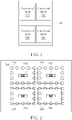
- FIG. 1 shows an exemplary block diagram of a semiconductor device according to an embodiment of the invention.
- the semiconductor device 100 may comprise multiple functional blocks, such as the functional blocks 110, 120, 130 and 140.
- Each functional block is configured to provide at least a predetermined function.
- each functional block may be equipped with a corresponding capacitive device, such as a capacitor or a decoupling capacitor, disposed physically proximate the corresponding functional block.
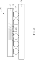
- FIG. 2 shows an exemplary perspective view of a semiconductor device according to an embodiment of the invention.
- each functional block may be implemented as a silicon die, such as the silicon dies 210, 220, 230 and 240.
- the silicon dies 210, 220, 230 and 240 may be disposed on a substrate or a thin film redistribution layer (RDL), depending on the process and/or packaging technology, and the substrate or the thin film RDL may be further connected to a printed circuit board (PCB) via solder balls.
- RDL thin film redistribution layer
- each silicon die may be equipped with a corresponding capacitive device, such as the capacitive device 215, 225, 235 and 245.
- the capacitive device 215 is disposed physically proximate the silicon die 210 (as well as the corresponding functional block).
- the capacitive device 225 is disposed physically proximate the silicon die 220 (as well as the corresponding functional block).
- the capacitive device 235 is disposed physically proximate the silicon die 230 (as well as the corresponding functional block).
- the capacitive device 245 is disposed physically proximate the silicon die 240 (as well as the corresponding functional block).
- the capacitive device 215, 225, 235 and 245 may be implemented as the capacitors attached on the land side under the die shadow (land-side capacitor, LSC) or adjacent to the die side (die-side capacitor, DSC).
- FIG. 3 shows an exemplary section view of a semiconductor device, for illustrating one possible placement of the capacitive device when adopting the Fan-Out Wafer-Level Packaging (WLP) technology, according to an embodiment of the invention.
- the semiconductor device 300 may comprise a silicon die 31 disposed on one side of the thin film RDL 32.
- the capacitive device 35 physically proximate the silicon die 31 may be disposed on an opposite side of the thin film RDL 32.
- the thin film RDL 32 may be connected to the PCB 34 via one or more solder balls 33.
- the capacitive device 35 may be a decoupling capacitor configured for the silicon die 31 to reduce the power noise and provide a relatively stable power supply.
- the capacitive device 35 in FIG. 3 may be any of the corresponding capacitive devices 215, 225, 235 and 245 in FIG. 2 .
- FIG. 4 shows an exemplary section view of a semiconductor device, for illustrating another possible placement of the capacitive device when adopting the flip chip packaging technology, according to another embodiment of the invention.
- the semiconductor device 400 may comprise a silicon die 41 disposed on a flip chip substrate 46.
- the silicon die 41 may be connected to one side of the flip chip substrate 46 via one or more solder balls 42.
- the capacitive device 45 physically proximate the silicon die 41 may be disposed on an opposite side of the flip chip substrate 46.
- the flip chip substrate 46 may be connected to the PCB 44 via one or more solder balls 43.
- the capacitive device 45 may be a decoupling capacitor configured for the silicon die 41 to reduce the power noise and provide a relatively stable power supply.
- the capacitive device 45 in FIG. 4 may be any of the corresponding capacitive devices 215, 225, 235 and 245 in FIG. 2 .
- one or more coupling paths may be introduced and configured in the corresponding semiconductor device, so as to implement the proposed method for sharing the capacitive devices among multiple functional blocks or silicon dies.
- FIG. 5 is a schematic diagram showing the equivalent circuit of a semiconductor device with one coupling path configured for sharing the capacitive devices among multiple functional blocks according to an embodiment of the invention.
- the semiconductor device 500 may comprise functional blocks 510, 520, 530 and 540, capacitive devices 515, 525, 535 and 545, switch devices 513, 523, 533 and 543 and a coupling path 550.
- Each functional block is configured to provide at least a predetermined function and is equipped with a corresponding capacitive device, such as a capacitor or a decoupling capacitor, disposed physically proximate the corresponding functional block.
- a capacitive device such as a capacitor or a decoupling capacitor
- the capacitive device 515 is disposed physically proximate the functional block 510
- the capacitive device 525 is disposed physically proximate the functional block 520
- the capacitive device 535 is disposed physically proximate the functional block 530
- the capacitive device 545 is disposed physically proximate the functional block 540.
- the way to make a capacitive device physically proximate to a functional block may refer to the schematic diagram as shown in FIG. 3 or FIG. 4 .
- the coupling path 550 may comprise connection nodes N1, N2 and N3, where the connection nodes N1, N2 and N3 are all connected to the functional block 510.
- the switch device 513 is connected to the capacitive device 515 and is controlled to selectively connect the capacitive device 515 to the connection node N1.
- the switch device 523 is connected to the capacitive device 525 and is controlled to selectively connect the capacitive device 525 to the functional block 520 or the connection node N2. To be more specific, the switch device 523 may be controlled to connect the capacitive device 525 to the switching node SN2-1 or the switching node SN2-2, where the switching node SN2-1 is connected to the functional block 520 and the switching node SN2-2 is connected to the connection node N2.
- the switch device 533 is connected to the capacitive device 535 and is controlled to selectively connect the capacitive device 535 to the functional block 530 or the connection node N3.
- the switch device 533 may be controlled to connect the capacitive device 535 to the switching node SN3-1 or the switching node SN3-2, where the switching node SN3-1 is connected to the functional block 530 and the switching node SN3-2 is connected to the connection node N3.
- the switch device 543 may be controlled to connect the capacitive device 545 to the switching node SN4-1 or the switching node SN4-2, where the switching node SN4-1 is connected to the functional block 540 and the switching node SN4-2 is connected to the connection node N3.
- the semiconductor device 500 may be a multi-core processor chip, and the functional blocks 510 ⁇ 540 may be respectively a processing core of the multi-core processor chip.
- the semiconductor device 500 may be a chip device, and the functional blocks 510 ⁇ 540 may be different processing units, as examples but not limited to, the Central Processing Unit (CPU), the Graphic Processing Unit (GPU), the Neural Processing Unit (NPU)... etc., of the chip device.
- the functional block 510 may be a master functional block, such as a big core or a master processing unit. However, whether to design one functional block as a master functional block is not a limit of the invention.
- the corresponding switch devices 523 ⁇ 543 may be controlled, as an example but not limited to, under the control of the functional block 510, to connect the corresponding capacitive devices 525 ⁇ 545 to the switching nodes SN2-2 ⁇ SN4-2, thereby coupling the corresponding capacitive device to the connection node N2 and/or N3 (as well as to the connection node N1 and the functional block 510).
- the switch device 523 may be controlled, as an example but not limited to, under the control of the functional block 510, to connect the capacitive device 525 to the switching node SN2-2, thereby coupling the corresponding capacitive device 525 to the connection node N2, which will be then connected to the connection node N1 and the functional block 510.
- the capacitive device 525 configured for the functional block 520 is shared with and provided for the functional block 510 as a supplementary capacitive device thereof.
- the mechanisms of controlling the switch devices 533 and 543 may be deduced by analogy.
- more than one of the capacitive devices configured for the corresponding functional blocks 520 ⁇ 540 may be shared with and provided for the functional block 510 in the similar manner.
- to connect how many capacitive devices to the functional block 510 may be flexibly controlled based on the actual loading of the functional block 510.
- the switch devices 523 ⁇ 543 may be controlled, as an example but not limited to, under the control of the functional block 510, to connect the corresponding capacitive devices 525 ⁇ 545 to the switching nodes SN2-2 ⁇ SN4-2, thereby coupling the corresponding capacitive device to the connection node N2 and/or N3 (as well as to the connection node N1 and the functional block 510).
- the switch device 523 may be controlled, as an example but not limited to, under the control of the functional block 510, to connect the capacitive device 525 to the switching node SN2-2, thereby coupling the corresponding capacitive device 525 to the connection node N2, and then to the connection node N1 and the functional block 510.
- the capacitive device 525 configured for the functional block 520 is shared with and provided for the functional block 510 as a supplementary capacitive device thereof.
- the mechanisms of controlling the switch devices 533 and 543 may be deduced by analogy.
- the capacitive devices corresponding to said more than one of the functional blocks 520 ⁇ 540 may be flexibly controlled to be connected to the functional block 510.
- 4 levels such as level 1 ⁇ level 4, may be set to define the loading of the functional block 510.
- the functional block 510 is determined functioning in the load condition of level 1, no supplementary capacitive device is required.
- the functional block 510 is determined functioning in the load condition of level 2
- one supplementary capacitive device may be required.
- two supplementary capacitive devices may be required.
- three supplementary capacitive devices may be required.
- the corresponding number of switch devices may be controlled to connect the corresponding capacitive devices to the functional block 510 via the corresponding switching nodes, connection nodes and the coupling path 550 by the way as described above.
- 4 share conditions such as share condition 1 ⁇ share condition 4 may be set to define how to share the capacitive devices with the functional block 510.
- the share condition 1 is satisfied and no capacitive device will be shared with the functional block 510.
- the share condition 2 is satisfied and the capacitive device corresponding to (that is, configured for) the non-functioning functional block, will be shared with and provided for the functional block 510 via the corresponding switching node, connection node and coupling path 550 by the way as described above.
- the share condition 3 is satisfied and the capacitive devices corresponding to (that is, configured for) the non-functioning functional blocks, will be shared with and provided for the functional block 510 via the corresponding switching nodes, connection nodes and coupling path 550 by the way as described above.
- the share condition 4 is satisfied and the capacitive devices corresponding to (that is, configured for) the non-functioning functional blocks, will be shared with and provided for the functional block 510 via the corresponding switching nodes, connection nodes and coupling path 550 by the way as described above.
- FIG. 6 is a schematic diagram showing the equivalent circuit of a semiconductor device with two coupling paths configured for sharing the capacitive devices among multiple functional blocks according to another embodiment of the invention.
- the semiconductor device 600 may comprise functional blocks 610, 620, 630 and 640, capacitive devices 615, 625, 635 and 645, switch devices 613, 623, 633 and 643 and two coupling paths 650 and 660.
- the equivalent circuit of the semiconductor device 600 is similar to that of the semiconductor device 500, except for that one more coupling path 660 is introduced.
- the coupling path 660 may comprise connection nodes N4 and N5, where the connection nodes N4 and N5 are all connected to the functional block 620.
- connection nodes N4 and N5 are all connected to the functional block 620.
- connection nodes N4 and N5 are all connected to the functional block 620.
- connection nodes N4 and N5 are all connected to the functional block 620.
- Like reference numbers in FIG. 5 and FIG. 6 may indicate similar or functionally similar elements. Therefore, some descriptions are omitted here for brevity.
- the switch device 613 is connected to the capacitive device 615 and is controlled to selectively connect the capacitive device 615 to the connection node N1 or connection node N4.
- the switch device 623 is connected to the capacitive device 625 and is controlled to selectively connect the capacitive device 625 to the connection node N2 or the connection node N4.
- the switch device 633 is connected to the capacitive device 635 and is controlled to selectively connect the capacitive device 635 to the functional block 630, the connection node N3 or the connection node N5.
- the switch device 643 is connected to the capacitive device 645 and is controlled to selectively connect the capacitive device 645 to the functional block 640, the connection node N3 or the connection node N5.
- the switch devices 633 and 643 may be controlled to be switched among three switching nodes.
- the switch device 613 may be further controlled to selectively connect the capacitive device 615 to the connection node N1 or the fourth connection node N4, and when the second functional block is determined in a heavy load condition, the switch device 613 may be controlled to connect the capacitive device 615 to the connection node N2, and then to the functional block 620.
- the capacitive device 615 configured for the functional block 610 is shared with and provided to the functional block 620 as a supplementary capacitive device thereof.
- the mechanisms of controlling the switch devices 633 and 643 may be deduced by analogy.
- the semiconductor device 600 may be a multi-core processor chip, and the functional blocks 610 ⁇ 640 may be respectively a processing core of the multi-core processor chip.
- the semiconductor device 600 may be a chip device, and the functional blocks 610 ⁇ 640 may be different processing units, as examples but not limited to, the CPU, the GPU, the NPU... etc., of the chip device.
- the functional block 610 may be a master functional block, such as a big core or a master processing unit. However, whether to design one functional block as a master functional block is not a limit of the invention.
- the corresponding switch devices 613, 633 and 643 may be controlled, as an example but not limited to, under the control of the functional block 620 or the functional block 610, to connect the corresponding capacitive devices 615, 635 and 645 to the connection nodes N4 or N5 (and then to the functional block 620).
- the switch devices 613, 633 and 643 may be controlled, as an example but not limited to, under the control of the functional block 620 or the functional block 610, to connect the corresponding capacitive devices 615, 635 and 645 to the connection nodes N4 or N5 (and then to the functional block 620).
- the capacitive devices corresponding to said more than one of the functional blocks 610, 630 and 640 may be flexibly controlled to be connected to the functional block 620.
- the coupling paths 550, 650 and 660 may be implemented by traces, cooper or metal lines or any other signal transmission lines.
- FIG. 7 shows an exemplary flow chart of a method or sharing capacitive devices among multiple functional blocks according to an embodiment of the invention.
- the proposed method may comprise the following steps:
- Step S706 may further comprise: determining whether the first functional block is in a heavy load condition; and controlling the second capacitive device to connect to the second connection node when the first functional block is determined in the heavy load condition.
- the method may further comprise an optional step: controlling a third capacitive device to connect to a third connection node when a third functional block is not functioning, wherein the third connection node is disposed on the first coupling path and connecting to the first connection node and the third capacitive device is disposed physically proximate the third functional block.
- the method may further comprise some optional steps: configuring a second coupling path comprising at least a fourth connection node, wherein the fourth connection node is connected to the second functional block; controlling the second capacitive device to connect to the fourth connection node when the second functional block is functioning; controlling the first capacitive device to connect to the fourth connection node when the first functional block is not functioning; and controlling a third capacitive device to connect to a fifth connection node when a third functional block is not functioning, wherein the fifth connection node is disposed on the second coupling path and connecting to the fourth connection node and the third capacitive device is disposed physically proximate the third functional block.
Landscapes
- Semiconductor Integrated Circuits (AREA)
- Engineering & Computer Science (AREA)
- Power Engineering (AREA)
- Semiconductor Memories (AREA)
Abstract
Description
- This application claims the benefit of
U.S. Provisional Application No. 63/180,148, filed on April 27th, 2021 - Decoupling capacitor is a capacitor installed at power supply end of a component in a circuit. This capacitor can provide a relatively stable power supply, and at the same time, it can reduce the noise coupled from the component to the power supply terminal (that is, decoupling the noise), which can indirectly reduce the influence of other components by the noise of this component. Large decoupling capacitor usually provides greater power noise reduction performance. However, the cost gets higher and the circuit area increases as well.
- With the explosion of mobile phones, tablets and other portable electronic devices, the need for smaller form factor products with better electrical performance motivates the research in the decoupling capacitor design. Therefore, a semiconductor device with flexibility in capacitor design to achieve better electrical performance is highly required.
- A semiconductor device according to the invention and a method for sharing capacitive devices among multiple functional blocks according to the invention are defined in the independent claims. The dependent claims define preferred embodiments thereof. According to an embodiment of the invention, a semiconductor device comprises a first functional block, a second functional block, a first capacitive device, a second capacitive device, a first coupling path, a first switch device and a second switch device. The first functional block is configured to provide at least a first predetermined function. The second functional block is configured to provide at least a second predetermined function. The first capacitive device is disposed physically proximate the first functional block. The second capacitive device is disposed physically proximate the second functional block. The first coupling path comprises at least a first connection node connecting to the first functional block. The first switch device is coupled to the first capacitive device and controlled to selectively connect the first capacitive device to the first connection node. The second switch device is coupled to the second capacitive device and controlled to selectively connect the second capacitive device to the second functional block or a second connection node. The second connection node is disposed on the first coupling path and connecting to the first connection node.
- According to another embodiment of the invention, a semiconductor device comprises a first functional block, a second functional block, a first capacitive device, a second capacitive device, a first coupling path, a first switch device and a second switch device. The first functional block is configured to provide at least a first predetermined function. The second functional block is configured to provide at least a second predetermined function. The first capacitive device is disposed physically proximate the first functional block. The second capacitive device is disposed physically proximate the second functional block. The first coupling path comprises at least a first connection node connecting to the first functional block. The first switch device is coupled to the first capacitive device and controlled to selectively connect the first capacitive device to the first connection node. The second switch device is coupled to the second capacitive device and controlled to selectively connect the second capacitive device to the second functional block or a second connection node. The second connection node is disposed on the first coupling path and connecting to the first connection node. When the first functional block is determined in a heavy load condition, the second switch device is controlled to connect the second capacitive device to the second connection node under control of the first functional block.
- According to yet another embodiment of the invention, a method for sharing capacitive devices among multiple functional blocks includes: configuring a first coupling path comprising at least a first connection node and a second connection node, wherein the first connection node is connected to the second connection node and further connected to a first functional block; controlling a first capacitive device to connect to the first functional block when the first functional block is functioning, wherein the first capacitive device is disposed physically proximate the first functional block; and controlling a second capacitive device to connect to the second connection node when a second functional block is not functioning, wherein the second capacitive device is disposed physically proximate the second functional block.
- These and other objectives of the present invention will no doubt become obvious to those of ordinary skill in the art after reading the following detailed description of the preferred embodiment that is illustrated in the various figures and drawings.
-
-
FIG. 1 shows an exemplary block diagram of a semiconductor device according to an embodiment of the invention. -
FIG. 2 shows an exemplary perspective view of a semiconductor device according to an embodiment of the invention. -
FIG. 3 shows an exemplary section view of a semiconductor device according to an embodiment of the invention. -
FIG. 4 shows an exemplary section view of a semiconductor device according to another embodiment of the invention. -
FIG. 5 is a schematic diagram showing the equivalent circuit of a semiconductor device with one coupling path configured for sharing the capacitive devices among multiple functional blocks according to an embodiment of the invention. -
FIG. 6 is a schematic diagram showing the equivalent circuit of a semiconductor device with two coupling paths configured for sharing the capacitive devices among multiple functional blocks according to another embodiment of the invention. -
FIG. 7 shows an exemplary flow chart of a method or sharing capacitive devices among multiple functional blocks according to an embodiment of the invention. -
FIG. 1 shows an exemplary block diagram of a semiconductor device according to an embodiment of the invention. Thesemiconductor device 100 may comprise multiple functional blocks, such as thefunctional blocks -
FIG. 2 shows an exemplary perspective view of a semiconductor device according to an embodiment of the invention. In the embodiments of the invention, each functional block may be implemented as a silicon die, such as the silicon dies 210, 220, 230 and 240. The silicon dies 210, 220, 230 and 240 may be disposed on a substrate or a thin film redistribution layer (RDL), depending on the process and/or packaging technology, and the substrate or the thin film RDL may be further connected to a printed circuit board (PCB) via solder balls. - According to an embodiment of the invention, each silicon die may be equipped with a corresponding capacitive device, such as the
capacitive device capacitive device 215 is disposed physically proximate the silicon die 210 (as well as the corresponding functional block). Thecapacitive device 225 is disposed physically proximate the silicon die 220 (as well as the corresponding functional block). Thecapacitive device 235 is disposed physically proximate the silicon die 230 (as well as the corresponding functional block). Thecapacitive device 245 is disposed physically proximate the silicon die 240 (as well as the corresponding functional block). In the embodiments of the invention, thecapacitive device -
FIG. 3 shows an exemplary section view of a semiconductor device, for illustrating one possible placement of the capacitive device when adopting the Fan-Out Wafer-Level Packaging (WLP) technology, according to an embodiment of the invention. Thesemiconductor device 300 may comprise asilicon die 31 disposed on one side of thethin film RDL 32. Thecapacitive device 35 physically proximate thesilicon die 31 may be disposed on an opposite side of thethin film RDL 32. Thethin film RDL 32 may be connected to the PCB 34 via one ormore solder balls 33. In this embodiment, thecapacitive device 35 may be a decoupling capacitor configured for thesilicon die 31 to reduce the power noise and provide a relatively stable power supply. The silicon die 31 inFIG. 3 may be any of the silicon dies 210, 220, 230 and 240 inFIG. 2 , and thecapacitive device 35 inFIG. 3 may be any of the correspondingcapacitive devices FIG. 2 . -
FIG. 4 shows an exemplary section view of a semiconductor device, for illustrating another possible placement of the capacitive device when adopting the flip chip packaging technology, according to another embodiment of the invention. Thesemiconductor device 400 may comprise a silicon die 41 disposed on aflip chip substrate 46. The silicon die 41 may be connected to one side of theflip chip substrate 46 via one ormore solder balls 42. Thecapacitive device 45 physically proximate the silicon die 41 may be disposed on an opposite side of theflip chip substrate 46. Theflip chip substrate 46 may be connected to thePCB 44 via one ormore solder balls 43. In this embodiment, thecapacitive device 45 may be a decoupling capacitor configured for the silicon die 41 to reduce the power noise and provide a relatively stable power supply. The silicon die 41 inFIG. 4 may be any of the silicon dies 210, 220, 230 and 240 inFIG. 2 , and thecapacitive device 45 inFIG. 4 may be any of the correspondingcapacitive devices FIG. 2 . - According to an embodiment of the invention, in order to provide flexibility in capacitor design so as to achieve better electrical performance for a semiconductor device, one or more coupling paths may be introduced and configured in the corresponding semiconductor device, so as to implement the proposed method for sharing the capacitive devices among multiple functional blocks or silicon dies.
-
FIG. 5 is a schematic diagram showing the equivalent circuit of a semiconductor device with one coupling path configured for sharing the capacitive devices among multiple functional blocks according to an embodiment of the invention. Thesemiconductor device 500 may comprisefunctional blocks capacitive devices switch devices coupling path 550. - Each functional block is configured to provide at least a predetermined function and is equipped with a corresponding capacitive device, such as a capacitor or a decoupling capacitor, disposed physically proximate the corresponding functional block. As an example, the
capacitive device 515 is disposed physically proximate thefunctional block 510, thecapacitive device 525 is disposed physically proximate thefunctional block 520, thecapacitive device 535 is disposed physically proximate thefunctional block 530 and thecapacitive device 545 is disposed physically proximate thefunctional block 540. The way to make a capacitive device physically proximate to a functional block may refer to the schematic diagram as shown inFIG. 3 orFIG. 4 . - The
coupling path 550 may comprise connection nodes N1, N2 and N3, where the connection nodes N1, N2 and N3 are all connected to thefunctional block 510. Theswitch device 513 is connected to thecapacitive device 515 and is controlled to selectively connect thecapacitive device 515 to the connection node N1. Theswitch device 523 is connected to thecapacitive device 525 and is controlled to selectively connect thecapacitive device 525 to thefunctional block 520 or the connection node N2. To be more specific, theswitch device 523 may be controlled to connect thecapacitive device 525 to the switching node SN2-1 or the switching node SN2-2, where the switching node SN2-1 is connected to thefunctional block 520 and the switching node SN2-2 is connected to the connection node N2. - Similarly, the
switch device 533 is connected to thecapacitive device 535 and is controlled to selectively connect thecapacitive device 535 to thefunctional block 530 or the connection node N3. To be more specific, theswitch device 533 may be controlled to connect thecapacitive device 535 to the switching node SN3-1 or the switching node SN3-2, where the switching node SN3-1 is connected to thefunctional block 530 and the switching node SN3-2 is connected to the connection node N3. Similarly, theswitch device 543 may be controlled to connect thecapacitive device 545 to the switching node SN4-1 or the switching node SN4-2, where the switching node SN4-1 is connected to thefunctional block 540 and the switching node SN4-2 is connected to the connection node N3. - According to an embodiment of the invention, the
semiconductor device 500 may be a multi-core processor chip, and thefunctional blocks 510~540 may be respectively a processing core of the multi-core processor chip. According to another embodiment of the invention, thesemiconductor device 500 may be a chip device, and thefunctional blocks 510~540 may be different processing units, as examples but not limited to, the Central Processing Unit (CPU), the Graphic Processing Unit (GPU), the Neural Processing Unit (NPU)... etc., of the chip device. In an embodiment, thefunctional block 510 may be a master functional block, such as a big core or a master processing unit. However, whether to design one functional block as a master functional block is not a limit of the invention. - According to an embodiment of the invention, when any of the
functional blocks 520~540 is not functioning or is functioning but performing a relatively light loading task, thecorresponding switch devices 523~543 may be controlled, as an example but not limited to, under the control of thefunctional block 510, to connect the correspondingcapacitive devices 525~545 to the switching nodes SN2-2~SN4-2, thereby coupling the corresponding capacitive device to the connection node N2 and/or N3 (as well as to the connection node N1 and the functional block 510). - To be more specific, when
functional block 520 is not functioning or is functioning but performing a relatively light loading task, theswitch device 523 may be controlled, as an example but not limited to, under the control of thefunctional block 510, to connect thecapacitive device 525 to the switching node SN2-2, thereby coupling the correspondingcapacitive device 525 to the connection node N2, which will be then connected to the connection node N1 and thefunctional block 510. In this manner, thecapacitive device 525 configured for thefunctional block 520 is shared with and provided for thefunctional block 510 as a supplementary capacitive device thereof. The mechanisms of controlling theswitch devices - Note that in an embodiment of the invention, when the
functional block 510 is functioning and when more than one of thefunctional blocks 520~540 are not functioning or are functioning but performing a relatively light loading task, more than one of the capacitive devices configured for the correspondingfunctional blocks 520~540 may be shared with and provided for thefunctional block 510 in the similar manner. In the embodiments of the invention, to connect how many capacitive devices to thefunctional block 510 may be flexibly controlled based on the actual loading of thefunctional block 510. - According to another embodiment of the invention, when any of the
functional blocks 520~540 is not functioning or is functioning but performing a relatively light loading task, and when thefunctional block 510 is determined functioning in a relatively heavy load condition, theswitch devices 523~543 may be controlled, as an example but not limited to, under the control of thefunctional block 510, to connect the correspondingcapacitive devices 525~545 to the switching nodes SN2-2~SN4-2, thereby coupling the corresponding capacitive device to the connection node N2 and/or N3 (as well as to the connection node N1 and the functional block 510). - To be more specific, when
functional block 520 is not functioning or is functioning but performing a relatively light loading task and when thefunctional block 510 is determined functioning in a relatively heavy load condition, theswitch device 523 may be controlled, as an example but not limited to, under the control of thefunctional block 510, to connect thecapacitive device 525 to the switching node SN2-2, thereby coupling the correspondingcapacitive device 525 to the connection node N2, and then to the connection node N1 and thefunctional block 510. In this manner, thecapacitive device 525 configured for thefunctional block 520 is shared with and provided for thefunctional block 510 as a supplementary capacitive device thereof. The mechanisms of controlling theswitch devices - Similarly, in an embodiment of the invention, when the
functional block 510 is functioning in a relatively heavy load condition and when more than one of thefunctional blocks 520~540 are not functioning or are functioning but performing a relatively light loading task, the capacitive devices corresponding to said more than one of thefunctional blocks 520~540 may be flexibly controlled to be connected to thefunctional block 510. - According to an embodiment of the invention, 4 levels, such as level 1~level 4, may be set to define the loading of the
functional block 510. When thefunctional block 510 is determined functioning in the load condition of level 1, no supplementary capacitive device is required. When thefunctional block 510 is determined functioning in the load condition of level 2, one supplementary capacitive device may be required. When thefunctional block 510 is determined functioning in the load condition of level 3, two supplementary capacitive devices may be required. When thefunctional block 510 is determined functioning in the load condition of level 4, three supplementary capacitive devices may be required. When one or more supplementary capacitive devices are required, the corresponding number of switch devices may be controlled to connect the corresponding capacitive devices to thefunctional block 510 via the corresponding switching nodes, connection nodes and thecoupling path 550 by the way as described above. - According to another embodiment of the invention, 4 share conditions, such as share condition 1~share condition 4, may be set to define how to share the capacitive devices with the
functional block 510. As an example, when all the functional blocks are functioning, the share condition 1 is satisfied and no capacitive device will be shared with thefunctional block 510. When one functional block is not functioning, the share condition 2 is satisfied and the capacitive device corresponding to (that is, configured for) the non-functioning functional block, will be shared with and provided for thefunctional block 510 via the corresponding switching node, connection node andcoupling path 550 by the way as described above. When two functional blocks are not functioning, the share condition 3 is satisfied and the capacitive devices corresponding to (that is, configured for) the non-functioning functional blocks, will be shared with and provided for thefunctional block 510 via the corresponding switching nodes, connection nodes andcoupling path 550 by the way as described above. When three functional blocks are not functioning, the share condition 4 is satisfied and the capacitive devices corresponding to (that is, configured for) the non-functioning functional blocks, will be shared with and provided for thefunctional block 510 via the corresponding switching nodes, connection nodes andcoupling path 550 by the way as described above. - It is to be noted that although four functional blocks and four corresponding capacitive devices and switch devices are utilized in the examples for the ease of expression, the number of functional blocks as well as the corresponding capacitive devices and switch devices should not be limited to four, and may be any positive integer greater than 1.
-
FIG. 6 is a schematic diagram showing the equivalent circuit of a semiconductor device with two coupling paths configured for sharing the capacitive devices among multiple functional blocks according to another embodiment of the invention. Thesemiconductor device 600 may comprisefunctional blocks capacitive devices switch devices coupling paths - The equivalent circuit of the
semiconductor device 600 is similar to that of thesemiconductor device 500, except for that onemore coupling path 660 is introduced. Thecoupling path 660 may comprise connection nodes N4 and N5, where the connection nodes N4 and N5 are all connected to thefunctional block 620. Like reference numbers inFIG. 5 andFIG. 6 may indicate similar or functionally similar elements. Therefore, some descriptions are omitted here for brevity. - The
switch device 613 is connected to thecapacitive device 615 and is controlled to selectively connect thecapacitive device 615 to the connection node N1 or connection node N4. Theswitch device 623 is connected to thecapacitive device 625 and is controlled to selectively connect thecapacitive device 625 to the connection node N2 or the connection node N4. Theswitch device 633 is connected to thecapacitive device 635 and is controlled to selectively connect thecapacitive device 635 to thefunctional block 630, the connection node N3 or the connection node N5. Theswitch device 643 is connected to thecapacitive device 645 and is controlled to selectively connect thecapacitive device 645 to thefunctional block 640, the connection node N3 or the connection node N5. - Noted that in this embodiment, the
switch devices FIG. 5 , in this embodiment, theswitch device 613 may be further controlled to selectively connect thecapacitive device 615 to the connection node N1 or the fourth connection node N4, and when the second functional block is determined in a heavy load condition, theswitch device 613 may be controlled to connect thecapacitive device 615 to the connection node N2, and then to thefunctional block 620. In this manner, thecapacitive device 615 configured for thefunctional block 610 is shared with and provided to thefunctional block 620 as a supplementary capacitive device thereof. The mechanisms of controlling theswitch devices - According to an embodiment of the invention, the
semiconductor device 600 may be a multi-core processor chip, and thefunctional blocks 610~640 may be respectively a processing core of the multi-core processor chip. According to another embodiment of the invention, thesemiconductor device 600 may be a chip device, and thefunctional blocks 610~640 may be different processing units, as examples but not limited to, the CPU, the GPU, the NPU... etc., of the chip device. In an embodiment, thefunctional block 610 may be a master functional block, such as a big core or a master processing unit. However, whether to design one functional block as a master functional block is not a limit of the invention. - Similarly, according to an embodiment of the invention, in order to provide supplementary capacitive device to the
functional block 620, when any of thefunctional blocks corresponding switch devices functional block 620 or thefunctional block 610, to connect the correspondingcapacitive devices - According to another embodiment of the invention, when any of the
functional blocks functional block 620 is determined functioning in a relatively heavy load condition, theswitch devices functional block 620 or thefunctional block 610, to connect the correspondingcapacitive devices - In an embodiment of the invention, when the
functional block 620 is functioning (or, functioning in a relatively heavy load condition) and when more than one of thefunctional blocks functional blocks functional block 620. - Regarding the mechanism of using multiple levels to define the loading of the
functional block 620 and then controlling the switch devices corresponding to the remaining functional blocks to connect the corresponding capacitive devices to thefunctional block 620 via the switching nodes, connection nodes and thecoupling path 660, reference may be made to the paragraphs with respect toFIG. 5 , and are omitted here for brevity. - Similarly, regarding the mechanism of using multiple share conditions to define how to share the capacitive devices with the
functional block 620 and then controlling the switch devices corresponding to the remaining functional blocks to connect the corresponding capacitive devices to thefunctional block 620 via the switching nodes, connection nodes and thecoupling path 660, reference may be made to the corresponding paragraphs with respect toFIG. 5 , and are omitted here for brevity. - According to an embodiment of the invention, the
coupling paths - It is to be noted again that although four functional blocks and four corresponding capacitive devices and switch devices are utilized in the examples for the ease of expression, the number of functional blocks as well as the corresponding capacitive devices and switch devices should not be limited to four, and may be any positive integer greater than 1.
- In addition, although one or two coupling paths are utilized in the examples for expression, the invention should not be limited thereto. Since those skilled in the art will readily derive the structure of the semiconductor device with more than two coupling paths based on the teachings of
FIG. 5 andFIG. 6 , the corresponding drawing and descriptions are omitted here for brevity. -
FIG. 7 shows an exemplary flow chart of a method or sharing capacitive devices among multiple functional blocks according to an embodiment of the invention. The proposed method may comprise the following steps: - Step S702: Configuring a first coupling path comprising at least a first connection node and a second connection node connected to a first functional block.
- Step S704: Controlling a first capacitive device to connect to the first connection node as well as the first functional block when the first functional block is functioning, wherein the first capacitive device is disposed physically proximate the first functional block.
- Step S706: Controlling a second capacitive device to connect to the second connection node when a second functional block is not functioning, wherein the second capacitive device is disposed physically proximate the second functional block.
- In some embodiments of the invention, Step S706 may further comprise: determining whether the first functional block is in a heavy load condition; and controlling the second capacitive device to connect to the second connection node when the first functional block is determined in the heavy load condition.
- In addition, in some embodiments of the invention, the method may further comprise an optional step: controlling a third capacitive device to connect to a third connection node when a third functional block is not functioning, wherein the third connection node is disposed on the first coupling path and connecting to the first connection node and the third capacitive device is disposed physically proximate the third functional block.
- In addition, in some embodiments of the invention, the method may further comprise some optional steps: configuring a second coupling path comprising at least a fourth connection node, wherein the fourth connection node is connected to the second functional block; controlling the second capacitive device to connect to the fourth connection node when the second functional block is functioning; controlling the first capacitive device to connect to the fourth connection node when the first functional block is not functioning; and controlling a third capacitive device to connect to a fifth connection node when a third functional block is not functioning, wherein the fifth connection node is disposed on the second coupling path and connecting to the fourth connection node and the third capacitive device is disposed physically proximate the third functional block.
- Based on the proposed structures of a semiconductor device with flexibility in capacitor design, better electrical performance is achieved by sharing capacitive devices among functional blocks for one or more of the capacitive devices to be provided as supplementary capacitive devices when required.
- Those skilled in the art will readily observe that numerous modifications and alterations of the device and method may be made while retaining the teachings of the invention. Accordingly, the above disclosure should be construed as limited only by the metes and bounds of the appended claims.
Claims (15)
- A semiconductor device (500; 600), comprising:a first functional block (510; 610), configured to provide at least a first predetermined function;a second functional block (520; 620), configured to provide at least a second predetermined function;a first capacitive device (515; 615), disposed physically proximate the first functional block (510; 610);a second capacitive device (525; 625), disposed physically proximate the second functional block (520; 620);a first coupling path (550; 650), comprising at least a first connection node (N1) connecting to the first functional block (510; 610);a first switch device (513; 613), coupled to the first capacitive device (515; 615) and being controlled to selectively connect the first capacitive device (515; 615) to the first connection node (N1); anda second switch device (523; 623), coupled to the second capacitive device (525; 625) and being controlled to selectively connect the second capacitive device (525; 625) to the second functional block (520; 620) or a second connection node (N2),wherein the second connection node (N2) is disposed on the first coupling path (550; 650) and connecting to the first connection node (N1).
- The semiconductor device of claim 1, wherein when the first functional block (510; 610) is determined in a heavy load condition, the second switch device (523; 623) is controlled to connect the second capacitive device (525; 625) to the second connection node (N2), preferably under control of the first functional block (510; 610).
- The semiconductor device of claim 1 or 2, further comprising:a third functional block (530; 630), configured to provide at least a third predetermined function;a third capacitive device (535; 635), disposed physically proximate the third functional block (530; 630); anda third switch device (533; 633), coupled to the third capacitive device (535; 635) and being controlled to selectively connect the third capacitive device (535; 635) to the third functional block (530; 630) or a third connection node (N3),wherein the third connection node (N3) is disposed on the first coupling path (550; 650) and connecting to the first connection node (N1).
- The semiconductor device of claim 3, wherein when the first functional block (510; 610) is determined in a heavy load condition, the third switch device (533; 633) is controlled to connect the third capacitive device (535; 635) to the third connection node (N3), preferably under control of the first functional block (510; 610).
- The semiconductor device of any one of claims 1 to 4, further comprising:
a second coupling path (660), comprising at least a fourth connection node (N4) connecting to the second functional block (620). - The semiconductor device of claim 5, wherein the first switch device (613) is further controlled to selectively connect the first capacitive device (615) to the first connection node (N1) or the fourth connection node (N4), and when the second functional block (620) is determined in a heavy load condition, the first switch device (613) is controlled to connect the first capacitive device (615) to the fourth connection node (N4), preferably under control of the first functional block (610).
- The semiconductor device of claim 5 in combination with claim 3 or 4,wherein the third switch device (633) is further controlled to selectively connect the third capacitive device (635) to the third functional block (630), the third connection node (N3) or a fifth connection node (N5), andwherein the fifth connection node (N5) is disposed on the second coupling path (660) and connecting to the fourth connection node (N4), and when the second functional block (620) is determined in a heavy load condition, the third switch device (633) is controlled to connect the third capacitive device (635) to the fifth connection node (N5), preferably under control of the first functional block (610).
- The semiconductor device of any one of claims 1 to 7, wherein the semiconductor device (500; 600) is a multi-core processor chip, and the first functional block (510; 610) and the second functional block (520; 620) are respectively a processing core of the multi-core processor chip.
- The semiconductor device of any one of claims 1 to 7, wherein the semiconductor device (500; 600) is a chip device, and the first functional block (510; 610) and the second functional block (520; 620) are different processing units of the chip device.
- A method for sharing capacitive devices among multiple functional blocks, comprising:configuring a first coupling path comprising at least a first connection node and a second connection node (S702), wherein the first connection node is connected to the second connection node and further connected to a first functional block;controlling a first capacitive device to connect to the first functional block when the first functional block is functioning (S704), wherein the first capacitive device is disposed physically proximate the first functional block; andcontrolling a second capacitive device to connect to the second connection node when a second functional block is not functioning (S706), wherein the second capacitive device is disposed physically proximate the second functional block.
- The method of claim 10, wherein step of controlling the second capacitive device to connect to the second connection node when the second functional block is not functioning further comprises:determining whether the first functional block is in a heavy load condition; andcontrolling the second capacitive device to connect to the second connection node when the first functional block is determined in the heavy load condition.
- The method of claim 10 or 11, further comprising:controlling a third capacitive device to connect to a third connection node when a third functional block is not functioning,wherein the third connection node is disposed on the first coupling path and connecting to the first connection node and the third capacitive device is disposed physically proximate the third functional block.
- The method of any one of claims 10 to 12, further comprising:configuring a second coupling path comprising at least a fourth connection node, wherein the fourth connection node is connected to the second functional block;controlling the second capacitive device to connect to the fourth connection node when the second functional block is functioning;controlling the first capacitive device to connect to the fourth connection node when the first functional block is not functioning; andcontrolling a third capacitive device to connect to a fifth connection node when a third functional block is not functioning,wherein the fifth connection node is disposed on the second coupling path and connecting to the fourth connection node and the third capacitive device is disposed physically proximate the third functional block.
- The method of any one of claims 10 to 13, wherein the first functional block and the second functional block are respectively a processing core comprised in a multi-core processor chip.
- The method of any one of claims 10 to 13, wherein the first functional block and the second functional block are different processing units of a chip device.
Applications Claiming Priority (2)
| Application Number | Priority Date | Filing Date | Title |
|---|---|---|---|
| US202163180148P | 2021-04-27 | 2021-04-27 | |
| US17/727,825 US11804826B2 (en) | 2021-04-27 | 2022-04-25 | Semiconductor devices with flexibility in capacitor design for power noise reduction |
Publications (1)
| Publication Number | Publication Date |
|---|---|
| EP4084065A1 true EP4084065A1 (en) | 2022-11-02 |
Family
ID=81748300
Family Applications (1)
| Application Number | Title | Priority Date | Filing Date |
|---|---|---|---|
| EP22169927.5A Pending EP4084065A1 (en) | 2021-04-27 | 2022-04-26 | Semiconductor devices with flexibility in capacitor design for power noise reduction |
Country Status (3)
| Country | Link |
|---|---|
| US (1) | US11804826B2 (en) |
| EP (1) | EP4084065A1 (en) |
| TW (1) | TWI854223B (en) |
Citations (2)
| Publication number | Priority date | Publication date | Assignee | Title |
|---|---|---|---|---|
| US20040007918A1 (en) * | 2002-07-11 | 2004-01-15 | Clevenger Lawrence A. | Shared on-chip decoupling capacitor and heat-sink devices |
| US20090179669A1 (en) * | 2008-01-10 | 2009-07-16 | Bartley Gerald K | Techniques for Providing Switchable Decoupling Capacitors for an Integrated Circuit |
Family Cites Families (4)
| Publication number | Priority date | Publication date | Assignee | Title |
|---|---|---|---|---|
| KR100611506B1 (en) * | 2004-06-18 | 2006-08-11 | 삼성전자주식회사 | Decoupling capacitance control circuit of semiconductor memory device |
| US8338854B2 (en) * | 2009-03-31 | 2012-12-25 | Alpha And Omega Semiconductor Incorporated | TVS with low capacitance and forward voltage drop with depleted SCR as steering diode |
| US9459672B2 (en) * | 2013-06-28 | 2016-10-04 | International Business Machines Corporation | Capacitance management |
| US9929148B1 (en) * | 2017-02-22 | 2018-03-27 | Globalfoundries Inc. | Semiconductor device including buried capacitive structures and a method of forming the same |
-
2022
- 2022-04-25 US US17/727,825 patent/US11804826B2/en active Active
- 2022-04-26 EP EP22169927.5A patent/EP4084065A1/en active Pending
- 2022-04-27 TW TW111116009A patent/TWI854223B/en active
Patent Citations (2)
| Publication number | Priority date | Publication date | Assignee | Title |
|---|---|---|---|---|
| US20040007918A1 (en) * | 2002-07-11 | 2004-01-15 | Clevenger Lawrence A. | Shared on-chip decoupling capacitor and heat-sink devices |
| US20090179669A1 (en) * | 2008-01-10 | 2009-07-16 | Bartley Gerald K | Techniques for Providing Switchable Decoupling Capacitors for an Integrated Circuit |
Also Published As
| Publication number | Publication date |
|---|---|
| TWI854223B (en) | 2024-09-01 |
| US20220345113A1 (en) | 2022-10-27 |
| US11804826B2 (en) | 2023-10-31 |
| TW202243382A (en) | 2022-11-01 |
Similar Documents
| Publication | Publication Date | Title |
|---|---|---|
| US12051651B2 (en) | Size and efficiency of dies | |
| US9659850B2 (en) | Package substrate comprising capacitor, redistribution layer and discrete coaxial connection | |
| US20200107444A1 (en) | Compact semiconductor chip system and method | |
| US9232639B2 (en) | Non-uniform substrate stackup | |
| US11482481B2 (en) | Semiconductor device and system | |
| US20160093340A1 (en) | Compact microelectronic assembly having reduced spacing between controller and memory packages | |
| US9460990B1 (en) | Substrates and semiconductor packages including the same, electronic systems including the semiconductor packages, and memory cards including the semiconductor packages | |
| US12069805B2 (en) | Wideband millimeter wave via transition | |
| US11942412B2 (en) | Interposer with flexible portion | |
| US9824954B2 (en) | Semiconductor package comprising stacked integrated circuit chips having connection terminals and through electrodes symmetrically arranged | |
| US11804826B2 (en) | Semiconductor devices with flexibility in capacitor design for power noise reduction | |
| US20030223208A1 (en) | Power plane region of printed circuit board with power blocks having an arc-shaped boundary | |
| WO2018125493A1 (en) | Programmable redistribution die | |
| US8406005B2 (en) | Printed circuit board | |
| KR102188644B1 (en) | Semiconductor package having extanded bandwidth | |
| US11877403B2 (en) | Printed wiring-board islands for connecting chip packages and methods of assembling same | |
| US6812409B2 (en) | Layer allocating apparatus for multi-layer circuit board | |
| CN115360187A (en) | Semiconductor device and method for sharing capacitor device between functional blocks | |
| US20240332222A1 (en) | Configurable semiconductor package capacitors and method | |
| US10002850B2 (en) | Semiconductor chip flexibly applied to various routing structures and semiconductor chip module using the same | |
| Gupta | Packaging design considerations for mobile and Internet of things (IOT) | |
| EP4643265A1 (en) | Apparatus, system, and method for integrating passive elements into electronic bridge components | |
| US9459672B2 (en) | Capacitance management | |
| US20080112142A1 (en) | Memory module comprising memory devices |
Legal Events
| Date | Code | Title | Description |
|---|---|---|---|
| PUAI | Public reference made under article 153(3) epc to a published international application that has entered the european phase |
Free format text: ORIGINAL CODE: 0009012 |
|
| STAA | Information on the status of an ep patent application or granted ep patent |
Free format text: STATUS: THE APPLICATION HAS BEEN PUBLISHED |
|
| AK | Designated contracting states |
Kind code of ref document: A1 Designated state(s): AL AT BE BG CH CY CZ DE DK EE ES FI FR GB GR HR HU IE IS IT LI LT LU LV MC MK MT NL NO PL PT RO RS SE SI SK SM TR |
|
| STAA | Information on the status of an ep patent application or granted ep patent |
Free format text: STATUS: REQUEST FOR EXAMINATION WAS MADE |
|
| 17P | Request for examination filed |
Effective date: 20230428 |
|
| RBV | Designated contracting states (corrected) |
Designated state(s): AL AT BE BG CH CY CZ DE DK EE ES FI FR GB GR HR HU IE IS IT LI LT LU LV MC MK MT NL NO PL PT RO RS SE SI SK SM TR |
|
| P01 | Opt-out of the competence of the unified patent court (upc) registered |
Effective date: 20230627 |