EP4081003A1 - Device comprising a circuit member sealed by a film - Google Patents
Device comprising a circuit member sealed by a film Download PDFInfo
- Publication number
- EP4081003A1 EP4081003A1 EP22165018.7A EP22165018A EP4081003A1 EP 4081003 A1 EP4081003 A1 EP 4081003A1 EP 22165018 A EP22165018 A EP 22165018A EP 4081003 A1 EP4081003 A1 EP 4081003A1
- Authority
- EP
- European Patent Office
- Prior art keywords
- film
- sealing member
- circuit member
- circuit
- present
- Prior art date
- Legal status (The legal status is an assumption and is not a legal conclusion. Google has not performed a legal analysis and makes no representation as to the accuracy of the status listed.)
- Granted
Links
Images





Classifications
-
- H—ELECTRICITY
- H10—SEMICONDUCTOR DEVICES; ELECTRIC SOLID-STATE DEVICES NOT OTHERWISE PROVIDED FOR
- H10W—GENERIC PACKAGES, INTERCONNECTIONS, CONNECTORS OR OTHER CONSTRUCTIONAL DETAILS OF DEVICES COVERED BY CLASS H10
- H10W74/00—Encapsulations, e.g. protective coatings
- H10W74/40—Encapsulations, e.g. protective coatings characterised by their materials
- H10W74/47—Encapsulations, e.g. protective coatings characterised by their materials comprising organic materials, e.g. plastics or resins
-
- A—HUMAN NECESSITIES
- A61—MEDICAL OR VETERINARY SCIENCE; HYGIENE
- A61B—DIAGNOSIS; SURGERY; IDENTIFICATION
- A61B5/00—Measuring for diagnostic purposes; Identification of persons
- A61B5/02—Detecting, measuring or recording for evaluating the cardiovascular system, e.g. pulse, heart rate, blood pressure or blood flow
- A61B5/024—Measuring pulse rate or heart rate
- A61B5/02444—Details of sensor
-
- B—PERFORMING OPERATIONS; TRANSPORTING
- B32—LAYERED PRODUCTS
- B32B—LAYERED PRODUCTS, i.e. PRODUCTS BUILT-UP OF STRATA OF FLAT OR NON-FLAT, e.g. CELLULAR OR HONEYCOMB, FORM
- B32B15/00—Layered products comprising a layer of metal
- B32B15/04—Layered products comprising a layer of metal comprising metal as the main or only constituent of a layer, which is next to another layer of the same or of a different material
- B32B15/08—Layered products comprising a layer of metal comprising metal as the main or only constituent of a layer, which is next to another layer of the same or of a different material of synthetic resin
-
- B—PERFORMING OPERATIONS; TRANSPORTING
- B32—LAYERED PRODUCTS
- B32B—LAYERED PRODUCTS, i.e. PRODUCTS BUILT-UP OF STRATA OF FLAT OR NON-FLAT, e.g. CELLULAR OR HONEYCOMB, FORM
- B32B27/00—Layered products comprising a layer of synthetic resin
- B32B27/06—Layered products comprising a layer of synthetic resin as the main or only constituent of a layer, which is next to another layer of the same or of a different material
- B32B27/08—Layered products comprising a layer of synthetic resin as the main or only constituent of a layer, which is next to another layer of the same or of a different material of synthetic resin
-
- B—PERFORMING OPERATIONS; TRANSPORTING
- B32—LAYERED PRODUCTS
- B32B—LAYERED PRODUCTS, i.e. PRODUCTS BUILT-UP OF STRATA OF FLAT OR NON-FLAT, e.g. CELLULAR OR HONEYCOMB, FORM
- B32B27/00—Layered products comprising a layer of synthetic resin
- B32B27/30—Layered products comprising a layer of synthetic resin comprising vinyl (co)polymers; comprising acrylic (co)polymers
- B32B27/304—Layered products comprising a layer of synthetic resin comprising vinyl (co)polymers; comprising acrylic (co)polymers comprising vinyl halide (co)polymers, e.g. PVC, PVDC, PVF, PVDF
-
- B—PERFORMING OPERATIONS; TRANSPORTING
- B32—LAYERED PRODUCTS
- B32B—LAYERED PRODUCTS, i.e. PRODUCTS BUILT-UP OF STRATA OF FLAT OR NON-FLAT, e.g. CELLULAR OR HONEYCOMB, FORM
- B32B27/00—Layered products comprising a layer of synthetic resin
- B32B27/30—Layered products comprising a layer of synthetic resin comprising vinyl (co)polymers; comprising acrylic (co)polymers
- B32B27/306—Layered products comprising a layer of synthetic resin comprising vinyl (co)polymers; comprising acrylic (co)polymers comprising vinyl acetate or vinyl alcohol (co)polymers
-
- B—PERFORMING OPERATIONS; TRANSPORTING
- B32—LAYERED PRODUCTS
- B32B—LAYERED PRODUCTS, i.e. PRODUCTS BUILT-UP OF STRATA OF FLAT OR NON-FLAT, e.g. CELLULAR OR HONEYCOMB, FORM
- B32B27/00—Layered products comprising a layer of synthetic resin
- B32B27/32—Layered products comprising a layer of synthetic resin comprising polyolefins
-
- B—PERFORMING OPERATIONS; TRANSPORTING
- B32—LAYERED PRODUCTS
- B32B—LAYERED PRODUCTS, i.e. PRODUCTS BUILT-UP OF STRATA OF FLAT OR NON-FLAT, e.g. CELLULAR OR HONEYCOMB, FORM
- B32B27/00—Layered products comprising a layer of synthetic resin
- B32B27/34—Layered products comprising a layer of synthetic resin comprising polyamides
-
- B—PERFORMING OPERATIONS; TRANSPORTING
- B32—LAYERED PRODUCTS
- B32B—LAYERED PRODUCTS, i.e. PRODUCTS BUILT-UP OF STRATA OF FLAT OR NON-FLAT, e.g. CELLULAR OR HONEYCOMB, FORM
- B32B27/00—Layered products comprising a layer of synthetic resin
- B32B27/36—Layered products comprising a layer of synthetic resin comprising polyesters
-
- B—PERFORMING OPERATIONS; TRANSPORTING
- B32—LAYERED PRODUCTS
- B32B—LAYERED PRODUCTS, i.e. PRODUCTS BUILT-UP OF STRATA OF FLAT OR NON-FLAT, e.g. CELLULAR OR HONEYCOMB, FORM
- B32B3/00—Layered products comprising a layer with external or internal discontinuities or unevennesses, or a layer of non-planar shape; Layered products comprising a layer having particular features of form
- B32B3/02—Layered products comprising a layer with external or internal discontinuities or unevennesses, or a layer of non-planar shape; Layered products comprising a layer having particular features of form characterised by features of form at particular places, e.g. in edge regions
- B32B3/04—Layered products comprising a layer with external or internal discontinuities or unevennesses, or a layer of non-planar shape; Layered products comprising a layer having particular features of form characterised by features of form at particular places, e.g. in edge regions characterised by at least one layer folded at the edge, e.g. over another layer ; characterised by at least one layer enveloping or enclosing a material
-
- H—ELECTRICITY
- H05—ELECTRIC TECHNIQUES NOT OTHERWISE PROVIDED FOR
- H05K—PRINTED CIRCUITS; CASINGS OR CONSTRUCTIONAL DETAILS OF ELECTRIC APPARATUS; MANUFACTURE OF ASSEMBLAGES OF ELECTRICAL COMPONENTS
- H05K1/00—Printed circuits
- H05K1/02—Details
- H05K1/14—Structural association of two or more printed circuits
- H05K1/144—Stacked arrangements of planar printed circuit boards
-
- H—ELECTRICITY
- H10—SEMICONDUCTOR DEVICES; ELECTRIC SOLID-STATE DEVICES NOT OTHERWISE PROVIDED FOR
- H10W—GENERIC PACKAGES, INTERCONNECTIONS, CONNECTORS OR OTHER CONSTRUCTIONAL DETAILS OF DEVICES COVERED BY CLASS H10
- H10W70/00—Package substrates; Interposers; Redistribution layers [RDL]
- H10W70/60—Insulating or insulated package substrates; Interposers; Redistribution layers
- H10W70/62—Insulating or insulated package substrates; Interposers; Redistribution layers characterised by their interconnections
- H10W70/65—Shapes or dispositions of interconnections
-
- H—ELECTRICITY
- H10—SEMICONDUCTOR DEVICES; ELECTRIC SOLID-STATE DEVICES NOT OTHERWISE PROVIDED FOR
- H10W—GENERIC PACKAGES, INTERCONNECTIONS, CONNECTORS OR OTHER CONSTRUCTIONAL DETAILS OF DEVICES COVERED BY CLASS H10
- H10W74/00—Encapsulations, e.g. protective coatings
- H10W74/10—Encapsulations, e.g. protective coatings characterised by their shape or disposition
- H10W74/111—Encapsulations, e.g. protective coatings characterised by their shape or disposition the semiconductor body being completely enclosed
-
- H—ELECTRICITY
- H10—SEMICONDUCTOR DEVICES; ELECTRIC SOLID-STATE DEVICES NOT OTHERWISE PROVIDED FOR
- H10W—GENERIC PACKAGES, INTERCONNECTIONS, CONNECTORS OR OTHER CONSTRUCTIONAL DETAILS OF DEVICES COVERED BY CLASS H10
- H10W74/00—Encapsulations, e.g. protective coatings
- H10W74/10—Encapsulations, e.g. protective coatings characterised by their shape or disposition
- H10W74/111—Encapsulations, e.g. protective coatings characterised by their shape or disposition the semiconductor body being completely enclosed
- H10W74/124—Encapsulations, e.g. protective coatings characterised by their shape or disposition the semiconductor body being completely enclosed the encapsulations having cavities other than that occupied by chips
-
- B—PERFORMING OPERATIONS; TRANSPORTING
- B32—LAYERED PRODUCTS
- B32B—LAYERED PRODUCTS, i.e. PRODUCTS BUILT-UP OF STRATA OF FLAT OR NON-FLAT, e.g. CELLULAR OR HONEYCOMB, FORM
- B32B2255/00—Coating on the layer surface
- B32B2255/10—Coating on the layer surface on synthetic resin layer or on natural or synthetic rubber layer
-
- B—PERFORMING OPERATIONS; TRANSPORTING
- B32—LAYERED PRODUCTS
- B32B—LAYERED PRODUCTS, i.e. PRODUCTS BUILT-UP OF STRATA OF FLAT OR NON-FLAT, e.g. CELLULAR OR HONEYCOMB, FORM
- B32B2255/00—Coating on the layer surface
- B32B2255/20—Inorganic coating
-
- B—PERFORMING OPERATIONS; TRANSPORTING
- B32—LAYERED PRODUCTS
- B32B—LAYERED PRODUCTS, i.e. PRODUCTS BUILT-UP OF STRATA OF FLAT OR NON-FLAT, e.g. CELLULAR OR HONEYCOMB, FORM
- B32B2255/00—Coating on the layer surface
- B32B2255/20—Inorganic coating
- B32B2255/205—Metallic coating
-
- B—PERFORMING OPERATIONS; TRANSPORTING
- B32—LAYERED PRODUCTS
- B32B—LAYERED PRODUCTS, i.e. PRODUCTS BUILT-UP OF STRATA OF FLAT OR NON-FLAT, e.g. CELLULAR OR HONEYCOMB, FORM
- B32B2307/00—Properties of the layers or laminate
- B32B2307/30—Properties of the layers or laminate having particular thermal properties
- B32B2307/31—Heat sealable
-
- H—ELECTRICITY
- H05—ELECTRIC TECHNIQUES NOT OTHERWISE PROVIDED FOR
- H05K—PRINTED CIRCUITS; CASINGS OR CONSTRUCTIONAL DETAILS OF ELECTRIC APPARATUS; MANUFACTURE OF ASSEMBLAGES OF ELECTRICAL COMPONENTS
- H05K2201/00—Indexing scheme relating to printed circuits covered by H05K1/00
- H05K2201/04—Assemblies of printed circuits
- H05K2201/041—Stacked PCBs, i.e. having neither an empty space nor mounted components in between
-
- H—ELECTRICITY
- H05—ELECTRIC TECHNIQUES NOT OTHERWISE PROVIDED FOR
- H05K—PRINTED CIRCUITS; CASINGS OR CONSTRUCTIONAL DETAILS OF ELECTRIC APPARATUS; MANUFACTURE OF ASSEMBLAGES OF ELECTRICAL COMPONENTS
- H05K2203/00—Indexing scheme relating to apparatus or processes for manufacturing printed circuits covered by H05K3/00
- H05K2203/08—Treatments involving gases
- H05K2203/082—Suction, e.g. for holding solder balls or components
-
- H—ELECTRICITY
- H05—ELECTRIC TECHNIQUES NOT OTHERWISE PROVIDED FOR
- H05K—PRINTED CIRCUITS; CASINGS OR CONSTRUCTIONAL DETAILS OF ELECTRIC APPARATUS; MANUFACTURE OF ASSEMBLAGES OF ELECTRICAL COMPONENTS
- H05K2203/00—Indexing scheme relating to apparatus or processes for manufacturing printed circuits covered by H05K3/00
- H05K2203/08—Treatments involving gases
- H05K2203/085—Using vacuum or low pressure
-
- H—ELECTRICITY
- H05—ELECTRIC TECHNIQUES NOT OTHERWISE PROVIDED FOR
- H05K—PRINTED CIRCUITS; CASINGS OR CONSTRUCTIONAL DETAILS OF ELECTRIC APPARATUS; MANUFACTURE OF ASSEMBLAGES OF ELECTRICAL COMPONENTS
- H05K2203/00—Indexing scheme relating to apparatus or processes for manufacturing printed circuits covered by H05K3/00
- H05K2203/13—Moulding and encapsulation; Deposition techniques; Protective layers
- H05K2203/1305—Moulding and encapsulation
- H05K2203/1311—Foil encapsulation, e.g. of mounted components
-
- H—ELECTRICITY
- H05—ELECTRIC TECHNIQUES NOT OTHERWISE PROVIDED FOR
- H05K—PRINTED CIRCUITS; CASINGS OR CONSTRUCTIONAL DETAILS OF ELECTRIC APPARATUS; MANUFACTURE OF ASSEMBLAGES OF ELECTRICAL COMPONENTS
- H05K2203/00—Indexing scheme relating to apparatus or processes for manufacturing printed circuits covered by H05K3/00
- H05K2203/13—Moulding and encapsulation; Deposition techniques; Protective layers
- H05K2203/1305—Moulding and encapsulation
- H05K2203/1327—Moulding over PCB locally or completely
-
- H—ELECTRICITY
- H10—SEMICONDUCTOR DEVICES; ELECTRIC SOLID-STATE DEVICES NOT OTHERWISE PROVIDED FOR
- H10W—GENERIC PACKAGES, INTERCONNECTIONS, CONNECTORS OR OTHER CONSTRUCTIONAL DETAILS OF DEVICES COVERED BY CLASS H10
- H10W72/00—Interconnections or connectors in packages
- H10W72/20—Bump connectors, e.g. solder bumps or copper pillars; Dummy bumps; Thermal bumps
- H10W72/241—Dispositions, e.g. layouts
- H10W72/242—Dispositions, e.g. layouts relative to the surface, e.g. recessed, protruding
-
- H—ELECTRICITY
- H10—SEMICONDUCTOR DEVICES; ELECTRIC SOLID-STATE DEVICES NOT OTHERWISE PROVIDED FOR
- H10W—GENERIC PACKAGES, INTERCONNECTIONS, CONNECTORS OR OTHER CONSTRUCTIONAL DETAILS OF DEVICES COVERED BY CLASS H10
- H10W72/00—Interconnections or connectors in packages
- H10W72/20—Bump connectors, e.g. solder bumps or copper pillars; Dummy bumps; Thermal bumps
- H10W72/261—Functions other than electrical connecting
-
- H—ELECTRICITY
- H10—SEMICONDUCTOR DEVICES; ELECTRIC SOLID-STATE DEVICES NOT OTHERWISE PROVIDED FOR
- H10W—GENERIC PACKAGES, INTERCONNECTIONS, CONNECTORS OR OTHER CONSTRUCTIONAL DETAILS OF DEVICES COVERED BY CLASS H10
- H10W74/00—Encapsulations, e.g. protective coatings
- H10W74/10—Encapsulations, e.g. protective coatings characterised by their shape or disposition
- H10W74/111—Encapsulations, e.g. protective coatings characterised by their shape or disposition the semiconductor body being completely enclosed
- H10W74/121—Encapsulations, e.g. protective coatings characterised by their shape or disposition the semiconductor body being completely enclosed by multiple encapsulations, e.g. by a thin protective coating and a thick encapsulation
-
- H—ELECTRICITY
- H10—SEMICONDUCTOR DEVICES; ELECTRIC SOLID-STATE DEVICES NOT OTHERWISE PROVIDED FOR
- H10W—GENERIC PACKAGES, INTERCONNECTIONS, CONNECTORS OR OTHER CONSTRUCTIONAL DETAILS OF DEVICES COVERED BY CLASS H10
- H10W90/00—Package configurations
- H10W90/701—Package configurations characterised by the relative positions of pads or connectors relative to package parts
- H10W90/721—Package configurations characterised by the relative positions of pads or connectors relative to package parts of bump connectors
- H10W90/722—Package configurations characterised by the relative positions of pads or connectors relative to package parts of bump connectors between stacked chips
Definitions
- This invention relates to a device comprising a circuit member sealed by a film.
- Patent Document 1 JP2001-332654A (Patent Document 1), the content of which is incorporated herein by reference.
- Patent Document 1 discloses a module (device) 90 with built-in semiconductor chips.
- the device 90 comprises a thermosetting resin composition (sealing resin) 92 and a circuit member 94 including semiconductor chips 96 and wiring patterns 98.
- the sealing resin 92 is formed so that the circuit member 94 is embedded therewithin. Then, a surface of the sealing resin 92 is polished so that the device 90 is made thinner.
- An aspect of the present invention provides a device comprising a first sealing member, a second sealing member, a first circuit member and a second circuit member.
- the first sealing member comprises, as a base of the first sealing member, a first film formed of a film and comprises a conductive portion made of conductor.
- the device is formed with a closed space. The closed space is enclosed by the first sealing member and the second sealing member and is shut off from an outer space located outside the device. The first circuit member and the second circuit member are shut in the closed space.
- the first circuit member comprises a first contact point.
- the second circuit member comprises a second contact point. The first contact point and the second contact point are pressed against each other to be in contact with each other in the closed space.
- At least one of the first circuit member and the second circuit member comprises an electrode. The conductive portion is in contact with the electrode in the closed space and is partially exposed to the outer space located outside the device.
- the present invention provides a device comprising a first sealing member, a second sealing member, a first circuit member and a second circuit member.
- the first sealing member comprises, as a base of the first sealing member, a first film formed of a film and comprises a conductive gel.
- the device is formed with a closed space. The closed space is enclosed by the first sealing member and the second sealing member and is shut off from an outer space located outside the device. The first circuit member and the second circuit member are shut in the closed space.
- the first circuit member comprises a first contact point.
- the second circuit member comprises a second contact point. The first contact point and the second contact point are pressed against each other to be in contact with each other in the closed space.
- At least one of the first circuit member and the second circuit member comprises an electrode.
- the conductive gel comprises a conductive portion. The conductive portion is in contact with the electrode in the closed space and is partially exposed to the outer space located outside the device.
- the first sealing member and the second sealing member overlap with each other while the first circuit member and the second circuit member (hereafter, simply referred to as "circuit members") are sandwiched therebetween.
- the first sealing member is basically formed of a film.
- the structure of each of the circuit members is not restricted except that the circuit members should be provided with the contact points and the electrode.
- each of the circuit members of an aspect of the present invention has a simple structure and can be formed of various material.
- each of the circuit members may be an insulation film formed with a conductive pattern having the contact point and the electrode. In this instance, the thickness of the entire device can be made extremely thin.
- an aspect of the present invention provides a new device which can be made thinner.
- a device 10 is an independent electronic device. More specifically, the device 10 can work solely without another electronic device (not shown) physically attached thereto. For example, the device 10 measures the heart rate of a subject by attaching the device 10 near the heart of the subject and transmits the measurement result to another electronic device. Thus, the device 10 can be used as an electronic device for measuring biological information such as heart rate.
- the present invention is not limited thereto but is applicable to various devices having various functions.
- the device 10 of the present embodiment comprises a circuit structure 12 and a sealing member 14.
- the circuit structure 12 is a member for enabling the device 10 to work as an electronic device.
- the circuit structure 12 has an electronic circuit (not shown) for receiving electric signals (hereafter, referred to as "biological signals") generated from electric pulse of the heart of the subject, another electronic circuit (not shown) for measuring the electric pulse of the heart based on the received biological signals and still another electronic circuit (not shown) for transmitting the measurement result to another electronic device (not shown).
- the sealing member 14 entirely accommodates the circuit structure 12 therewithin and protects the circuit structure 12 from an external environment. Thus, the circuit structure 12 is shut in the sealing member 14.
- the circuit structure 12 of the present embodiment comprises a first circuit member 40 and a second circuit member 50.
- the sealing member 14 of the present embodiment comprises a first sealing member 20 and a second sealing member 30.
- the device 10 comprises the first sealing member 20, the second sealing member 30, the first circuit member 40 and the second circuit member 50.
- the four members of the device 10 i.e., the first sealing member 20, the second sealing member 30, the first circuit member 40 and the second circuit member 50, are stacked in an upper-lower direction (Z-direction) and are combined to form the device 10 as a single structure.
- the device 10 of the present embodiment comprises only the aforementioned four members. However, the present invention is not limited thereto, but the device 10 may further comprise another member in addition to the aforementioned four members.
- the first sealing member 20 of the present embodiment is formed of, as a base thereof, a first film 22 which is an insulation film.
- the first sealing member 20 comprises, as a base of the first sealing member 20, the first film 22 formed of a film.
- the first film 22 of the present embodiment is a thin, rectangular sheet and is bendable.
- the first film 22 has a thickness of about 0.01 to 0.5 mm.
- the first film 22 extends in parallel to a horizontal plane (sheet plane: XY-plane).
- the first film 22 has a peripheral edge 229 in the XY-plane.
- the first film 22 has an outer surface 232 and an inner surface 234.
- the outer surface 232 is an upper surface (positive Z-side surface) of the first film 22.
- the inner surface 234 is a lower surface (negative Z-side surface) of the first film 22.
- the first film 22 of the present embodiment comprises two layers consisting of a meltable layer 146 which is meltable by heat-treatment and an unmeltable layer 148 which is not meltable by heat-treatment.
- the meltable layer 146 is located under the unmeltable layer 148.
- the meltable layer 146 is made of polyethylene, and the unmeltable layer 148 is made of nylon. According to this structure, the meltable layer 146 can be fused to another meltable layer of another member while the unmeltable layer 148 is maintained.
- the present invention is not limited thereto.
- the first film 22 may comprise only one layer which is the unmeltable layer 148 or may comprise three or more layers.
- the first film 22 is formed with a main opening 244 and a valve opening 248.
- Each of the main opening 244 and the valve opening 248 of the present embodiment has a small circular shape in the XY-plane and passes through the first film 22 in the Z-direction.
- the main opening 244 has a diameter of 0.5 mm or less.
- Each of the main opening 244 and the valve opening 248 as described above can be formed by a forming method such as laser irradiation.
- the present invention is not limited thereto.
- the shape and the size in the XY-plane of each of the main opening 244 and the valve opening 248 are not specifically limited.
- the first sealing member 20 of the present embodiment comprises a sub-member 26 and an air valve 28 in addition to the first film 22.
- the sub-member 26 of the present embodiment is a circular, thin sheet and is bendable.
- the sub-member 26 comprises a thin bondable portion 262 made of resin such as polyethylene terephthalate (PET) or polyurethane (PU) and a thin conductive portion 266 made of conductor such as metal.
- PET polyethylene terephthalate
- PU polyurethane
- the first sealing member 20 comprises the bondable portion 262 formed of a film and the thin film-like conductive portion 266.
- each of the bondable portion 262 and the conductive portion 266 of the present embodiment has a thickness of about 0.01 to 0.5 mm.
- the sub-member 26 is formed with a sub-opening 264.
- the sub-opening 264 has a small circular shape in the XY-plane.
- the sub-opening 264 has a diameter of 0.5 mm or less.
- the sub-opening 264 passes through the bondable portion 262 in the Z-direction. However, the sub-opening 264 is filled with the conductive portion 266 so that no gap is left. In other words, the conductive portion 266 extends over the whole sub-opening 264 in the XY-plane and shuts the sub-opening 264.
- the conductive portion 266 is exposed upward and downward. In other words, the positive Z-side surface and the negative Z-side surface of the conductive portion 266 are exposed outward. Thus, the sub-member 26 is formed so as to be electrically connectable in the Z-direction.
- the sub-member 26 of the present embodiment can be formed as described below.
- a film having a thickness of about 0.01 to 0.5 mm is formed of resin such as PET or PU.
- the film is formed with the sub-opening 264 having a diameter of 0.5 mm or less by a forming method such as laser irradiation.
- the bondable portion 262 is formed.
- the sub-opening 264 is filled with conductive paste which is spread on one of opposite surfaces of the film by using a proper mask and a doctor blade.
- the film is heated so that the conductive paste is hardened.
- the sub-opening 264 is filled with conductive paste which is spread on a remaining one of the opposite surfaces of the film by using a proper mask and the doctor blade. Then, the film is heated so that the conductive paste is hardened.
- the conductive portion 266 is formed of the conductive paste as a result of the aforementioned twice heat-treatment.
- the sub-member 26 of the present embodiment is formed as described above and has the aforementioned structure.
- the present invention is not limited thereto.
- the conductive portion 266 may be formed by plating or by ink-jetting.
- the conductive portion 266 may be formed of metal foil which is laminated on an upper or lower surface of the bondable portion 262 so as to cover the whole sub-opening 264.
- the conductive portion 266 may partially protrude downward.
- the shape and the size of the sub-member 26 are not specifically limited.
- the diameter of the main opening 244 of the first film 22 is smaller than the diameter of the bondable portion 262 of the sub-member 26 but is larger than the diameter of the conductive portion 266 of the sub-member 26.
- the bondable portion 262 of the present embodiment is bonded on the outer surface 232 so as to surround the main opening 244 in the XY-plane.
- a part of the bondable portion 262 which is located around the sub-opening 264 is bonded to the first film 22 throughout its entire circumference so as to surround the main opening 244.
- the bondable portion 262 is firmly attached to the outer surface 232 and seals the edge of the main opening 244 in the XY-plane throughout its entire circumference.
- the sub-member 26 entirely shuts the main opening 244 and blocks air which might flow through the main opening 244.
- the bondable portion 262 of the present embodiment is bonded on the outer surface 232 of the first film 22 by using a fixing member such as an adhesive.
- the first film 22 may further comprises another meltable layer (not shown) which is located over the unmeltable layer 148.
- the bondable portion 262 may comprise a meltable layer (not shown) and an unmeltable layer (not shown).
- the meltable layer of the bondable portion 262 may be a lower layer of the bondable portion 262. According to the aforementioned modification, the bondable portion 262 can be bonded on the outer surface 232 of the first film 22 by fusing the meltable layer of the bondable portion 262 and the meltable layer of the first film 22 to each other.
- the bondable portion 262 of the present embodiment has an outer edge in the XY-plane which is located outward of the main opening 244 in the XY-plane. Moreover, the bondable portion 262 has an inner edge in the XY-plane which is located inward of the main opening 244 in the XY-plane.
- the conductive portion 266 of the present embodiment is located inward of the main opening 244 in the XY-plane.
- the thus-arranged conductive portion 266 is vertically movable while the bondable portion 262 is resiliently deformed partially.
- the bondable portion 262 is made of PU, the bondable portion 262 is resiliently deformable easily.
- the present invention is not limited thereto. For example, relationship in size in the XY-plane among the bondable portion 262, the main opening 244 and the conductive portion 266 can be variously modified as necessary.
- the air valve 28 of the present embodiment comprises a cover portion 282 formed of a thin insulation film and a base portion 286 made of insulator.
- the base portion 286 is formed with a passing hole 288.
- the passing hole 288 passes through the base portion 286 in the Z-direction.
- the cover portion 282 is formed with five valves 284 and five cuts 285 which correspond to the valves 284, respectively. Each of the cuts 285 passes through the cover portion 282 in the Z-direction.
- the valves 284 and the cuts 285 are located inward of an outer circumference of the cover portion 282 in the XY-plane.
- the cover portion 282 is adhered to and fixed on an upper surface of the base portion 286.
- the outer circumference of the cover portion 282 in the XY-plane is tightly adhered to the upper surface of the base portion 286 throughout its entire circumference.
- an inner part of the cover portion 282, which is located inward of the outer circumference of the cover portion 282 in the XY-plane can be pulled away from the upper surface of the base portion 286.
- a passage which allows air to pass therethrough can be formed between the passing hole 288 and each of the cuts 285.
- the base portion 286 has a lower surface which is adhered to and fixed on the first film 22 in such a way that the passing hole 288 communicates with the valve opening 248 of the first film 22.
- the air valve 28 can take either an open state shown in Fig. 7 or a closed state shown in Fig.1 .
- each of the valves 284 is apart from the corresponding cut 285.
- each of the valves 284 completely covers the corresponding cut 285.
- an air passage via the air valve 28 is formed between the inside and the outside of the device 10.
- the air valve 28 takes the closed state the inside of the device 10 is shut off from the outside of the device 10.
- the air valve 28 is used for vacuuming the inside of the device 10 upon fabrication of the device 10.
- the air valve 28 of the present embodiment has a structure suitable for this use.
- the present invention is not limited thereto.
- the structure of the air valve 28 is not specifically limited, provided that the inside air of the device 10 can be discharged by using the air valve 28.
- the inside of the device 10 may be vacuumed without provision of the air valve 28.
- the air valve 28 may be provided as necessary.
- the second sealing member 30 of the present embodiment is formed of, as a base thereof, a second film 32 which is an insulation film.
- the second sealing member 30 comprises, as a base of the second sealing member 30, the second film 32 formed of a film.
- the second film 32 of the present embodiment is formed of material similar to that of the first film 22 and has a structure similar to that of the first film 22.
- the second film 32 is a thin, rectangular sheet and is bendable.
- the second film 32 extends in parallel to the XY-plane.
- the second film 32 has a peripheral edge 329 in the XY-plane.
- the present invention is not limited thereto.
- the second sealing member 30 may comprise, as a base thereof, a rigid circuit board instead of the second film 32.
- the rigid circuit board may have rigidity and may be hardly bent.
- the second film 32 or the rigid circuit board of the present embodiment comprises, similarly to the first film 22, two layers consisting of the meltable layer 146 which is meltable by heat-treatment and the unmeltable layer 148 which is not meltable by heat-treatment.
- the meltable layer 146 is located over the unmeltable layer 148.
- the two meltable layers 146 of the first film 22 and the second film 32 can be fused to each other while the unmeltable layers 148 are maintained.
- the present invention is not limited thereto.
- Each of the first film 22 and the second film 32 may have any structure, provided that it is in accordance with a forming method of the device 10.
- the first film 22 and the second film 32 may be bonded together by using a fixing member such as an adhesive.
- each of the first film 22 and the second film 32 may comprise only one layer which is the unmeltable layer 148.
- each of the first film 22 and the second film 32 may comprise three or more layers.
- the second sealing member 30 of the present embodiment comprises an additional film 38 formed of an insulation film in addition to the second film 32.
- the additional film 38 has an uneven portion 382.
- the uneven portion 382 is provided in order to maintain a passage which allows air to pass therethrough upon vacuuming the inside of the device 10.
- the uneven portion 382 is formed with a large number of projections 384.
- Each of the projections 384 is a projection which projects upward and is resiliently deformable.
- the projections 384 are uniformly and continuously formed over the entire additional film 38 in the XY-plane. According to the structure described above, a passage which allows air to pass therethrough is formed between every adjacent two of the projections 384.
- the shape and the size of each of the projections 384 are not specifically limited, provided that the passage which allows air to pass therethrough can be formed.
- the first film 22 and the second film 32 of the present embodiment overlap with each other so that the position of the peripheral edge 229 and the position of the peripheral edge 329 are aligned with each other in the XY-plane.
- the present invention is not limited thereto.
- the size of the first film 22 in the XY-plane and the size of the second film 32 in the XY-plane may be different from each other.
- the shape of each of the first film 22 and the second film 32 is not limited to be rectangular but can be modified as necessary.
- the first circuit member 40 of the present embodiment has a first base portion 42 and a first conductive pattern 44.
- the first base portion 42 of the present embodiment is a thin, rectangular sheet formed of an insulation film and is bendable.
- the first base portion 42 extends in parallel to the XY-plane.
- the first conductive pattern 44 is formed on the first base portion 42.
- the first conductive pattern 44 is made of conductor such as copper and is formed on a lower surface of the first base portion 42 by a forming method such as silver ink printing or etching.
- the second circuit member 50 of the present embodiment has a second base portion 52 and a second conductive pattern 54.
- the second base portion 52 of the present embodiment is a thin, rectangular sheet formed of an insulation film and is bendable.
- the second base portion 52 extends in parallel to the XY-plane.
- the second conductive pattern 54 is formed on the second base portion 52.
- the second conductive pattern 54 is made of conductor such as copper and is formed on an upper surface of the second base portion 52 by a forming method such as silver ink printing or etching.
- each of the first circuit member 40 and the second circuit member 50 of the present embodiment has the aforementioned structure.
- the present invention is not limited thereto.
- each of the first circuit member 40 and the second circuit member 50 may be provided with one or more electronic components.
- One of the first circuit member 40 and the second circuit member 50 may be a single electronic component.
- Each of the first circuit member 40 and the second circuit member 50 may be a rigid circuit board.
- the forming method of each of the first conductive pattern 44 and the second conductive pattern 54 is not specifically limited, provided that each of the first conductive pattern 44 and the second conductive pattern 54 is made of conductor.
- the first conductive pattern 44 of the present embodiment has a first contact point 48.
- the second conductive pattern 54 of the present embodiment has a second contact point 58 and an electrode 59.
- the first circuit member 40 comprises the first contact point 48
- the second circuit member 50 comprises the second contact point 58 and the electrode 59.
- the first contact point 48 and the second contact point 58 are in contact with each other in the fabricated device 10.
- the electrode 59 and the conductive portion 266 are in contact with each other in the fabricated device 10.
- the first conductive pattern 44 and the second conductive pattern 54 are electrically connected with each other and are electrically connectable with a member located outside the device 10 through the conductive portion 266.
- the first conductive pattern 44 and the second conductive pattern 54 illustrated in Fig. 6 are abstract conductive patterns for simple explanation about the present invention and have no specific function. In other words, even when the illustrated first contact point 48 and the illustrated second contact point 58 are brought into contact with each other, the device 10 does not work as an electronic device.
- the actual first conductive pattern 44 and the actual second conductive pattern 54 are formed with an electronic circuit (not shown) which can measure the electric pulse of the heart of the subject. Referring to Fig. 1 , this electronic circuit can obtain biological signals based on the electric pulse of the heart of the subject via the conductive portion 266.
- each of the number of the first contact point 48 and the number of the second contact point 58 of the present embodiment is one.
- each of the number of the electrode 59 and the number of the conductive portion 266 is one.
- the present invention is not limited thereto.
- each of the number of the first contact points 48 and the number of the second contact points 58 may be two or more.
- each of the number of the electrodes 59 and the number of the conductive portions 266 may be two or more.
- the first contact points 48 should be in contact with the second contact points 58, respectively, and the electrodes 59 should be in contact with the conductive portions 266, respectively.
- the first film 22 of the present embodiment has a first inner portion 222 and a first outer portion 224.
- the first outer portion 224 of the present embodiment has a first seal portion 226 and a first contact portion 228.
- the first inner portion 222 is located inward of the first outer portion 224 in the XY-plane. In other words, the first outer portion 224 is a part of the first film 22 which surrounds the first inner portion 222.
- the second film 32 of the present embodiment has a second inner portion 322 and a second outer portion 324.
- the second outer portion 324 of the present embodiment has a second seal portion 326 and a second contact portion 328.
- the second inner portion 322 is located inward of the second outer portion 324 in the XY-plane.
- the second outer portion 324 is a part of the second film 32 which surrounds the second inner portion 322.
- the first inner portion 222 of the first film 22 and the second inner portion 322 of the second film 32 of the device 10 are parts for accommodating the circuit structure 12 and are apart from each other.
- the first seal portion 226 and the second seal portion 326 of the present embodiment are bonded together to form a seal trace 16.
- the first seal portion 226 and the second seal portion 326 are bonded together by heat-sealing.
- the seal trace 16 of the present embodiment is a trace where the first seal portion 226 and the second seal portion 326 are welded to each other by heat-treatment.
- the present invention is not limited thereto, but the first seal portion 226 and the second seal portion 326 can be bonded together by various methods such as high frequency, ultrasonic, laser or adhesive.
- the seal trace 16 of the present embodiment is formed throughout entire circumference of the first seal portion 226 and the second seal portion 326.
- the seal trace 16 surrounds the first contact portion 228 and the second contact portion 328 throughout their entire circumference in the XY-plane.
- the present invention is not limited thereto, but the seal trace 16 may be formed on a necessary part in accordance with the forming method of the device 10.
- the seal trace 16 may be partially formed or may not be formed at all.
- the inside of the device 10 is vacuumed after the first seal portion 226 and the second seal portion 326 are bonded together.
- the first contact portion 228 and the second contact portion 328 are brought into contact with each other in a contact region 17 because of air pressure difference.
- the device 10 is formed with a closed space 18.
- the closed space 18 is enclosed by the first inner portion 222 and the second inner portion 322.
- the contact region 17 of the present embodiment seamlessly surrounds the first inner portion 222 and the second inner portion 322 throughout their entire circumference in the XY-plane.
- the present invention is not limited thereto, but the contact region 17 may be formed on a necessary part in accordance with the forming method of the device 10.
- the contact region 17 may be partially formed or may not be formed at all.
- the first seal portion 226 and the second seal portion 326 are firmly bonded together.
- the contact region 17 is located inward of the seal trace 16 in the XY-plane and blocks air which might flow between the inside and the outside of the closed space 18.
- air pressure in the closed space 18 is kept to low pressure lower than the atmospheric pressure.
- the first circuit member 40 and the second circuit member 50 are shut in the closed space 18 which is kept to the aforementioned low pressure.
- the first contact point 48 and the second contact point 58 are pressed against each other to be in contact with each other in the closed space 18.
- a contact force is generated between the first contact point 48 and the second contact point 58 because of air pressure difference between the inside and the outside of the closed space 18.
- the first contact point 48 and the second contact point 58 are pressed against each other because of this air pressure difference. Therefore, the contact between the first contact point 48 and the second contact point 58 can be securely kept.
- first sealing member 20 and the second sealing member 30 of the device 10 of the present embodiment overlap with each other to be in contact with each other while the first circuit member 40 and the second circuit member 50 (hereafter, simply referred to as "circuit members") are sandwiched therebetween.
- first sealing member 20 and the second sealing member 30 of the present embodiment is basically formed of a film.
- each of the circuit members has a simple structure and can be formed of various material.
- the circuit members may be two insulation films formed with the conductive patterns consisting of the first conductive pattern 44 and the second conductive pattern 54.
- the conductive patterns may merely have the contact points and the electrode 59.
- the thickness of the entire device 10 can be made extremely thin.
- the present embodiment provides the device 10 which is new and can be made thinner.
- the first seal portion 226 and the second seal portion 326 are bonded together, and the first contact portion 228 and the second contact portion 328 are in contact with each other. According to this structure, the closed space 18 can be reliably kept airtight.
- the present invention is not limited to the present embodiment.
- the first seal portion 226 and the second seal portion 326 may partially surround the first contact portion 228 and the second contact portion 328 in the XY-plane.
- the first seal portion 226 and the second seal portion 326 may partially surround the first inner portion 222 and the second inner portion 322 in the XY-plane.
- the first circuit member 40 and the second circuit member 50 can be easily taken out from the closed space 18 by cutting off the first seal portion 226 and the second seal portion 326.
- the members can be easily collected separately and can be reused.
- the conductive portion 266 of the present embodiment is in contact with the electrode 59 in the closed space 18 and is partially exposed to the outer space located outside the device 10.
- the outer surface 232 of the first film 22 is located outside the closed space 18.
- the bondable portion 262 of the sub-member 26 is bonded on the thus-arranged outer surface 232.
- the conductive portion 266 and the electrode 59 are pressed against each other because of air pressure difference between the inside and the outside of the closed space 18 so that the contact between the conductive portion 266 and the electrode 59 can be reliably kept.
- the electronic circuits (not shown) formed in the first conductive pattern 44 and the second conductive pattern 54 should obtain biological signals of a subject with no contact with the subject.
- the electronic circuits should obtain biological signals of the subject by contactless communication.
- weak biological signals are difficult to be accurately obtained by contactless communication.
- biological signals can be accurately obtained via the conductive portion 266 which is in contact with a skin of the subject.
- Each of the first sealing member 20 and the second sealing member 30 is preferred to have a high barrier property against oxygen. More specifically, each of the first film 22 and the second film 32 (or rigid circuit board) is preferred to comprise a layer made of high oxygen barrier material which is material having a high barrier property against oxygen. According to this layer-structure, oxidation of the metal members of the circuit structure 12 can be reduced.
- the high oxygen barrier material may be linear low-density polyethylene (LLDPE). More specifically, the high oxygen barrier material may be PET/AI/PE which is formed by laminating polyethylene terephthalate, aluminum and polyethylene; ON/PE which is formed by laminating biaxially stretched nylon and polyethylene; PET/EVOH/PE which is formed by laminating polyethylene terephthalate, polyvinyl chloride and polyethylene; or may be formed by laminating a transparent high barrier film and polyethylene.
- the transparent high barrier film may be polyethylene terephthalate (PET) deposited with SiOx or aluminum oxide.
- each of the first sealing member 20 and the second sealing member 30 of the present embodiment is preferred to have a high barrier property against water vapor in addition to the high barrier property against oxygen.
- each of the first film 22 and the second film 32 (or rigid circuit board) is preferred to comprise a layer made of high water-vapor barrier material which is material having a high barrier property against water vapor.
- the circuit structure 12 can be water-proofed.
- the high water-vapor barrier material may be material which is a sheet made of ON/PE, biaxially stretched polypropylene (OPP) or PET and is coated with polyvinylidene chloride (PVDC).
- Each of the first sealing member 20 and the second sealing member 30 may have various barrier properties such as a barrier property against nitrogen in addition to the high barrier property against oxygen and the high barrier property against water vapor.
- each of the first sealing member 20 and the second sealing member 30 is preferred to have high barrier properties in accordance with its use.
- the device 10 (see Fig. 1 ) of the present embodiment is formed via four steps consisting of a preparing step (STEP 1), a stacking step (STEP 2), a shutting-in step (STEP 3) and a vacuuming step (STEP 4).
- a preparing step STEP 1
- a stacking step STEP 2
- a shutting-in step STP 3
- a vacuuming step STP 4
- the present invention is not limited thereto, but the forming method of the device 10 can be modified as necessary.
- explanation will be made about an example of the forming method of the device 10 of the present embodiment.
- the first sealing member 20, the second sealing member 30, the first circuit member 40 and the second circuit member 50 are prepared.
- the first sealing member 20, the first circuit member 40, the second circuit member 50 and the second sealing member 30 are stacked on each other in this order from top to bottom along the Z-direction.
- the first circuit member 40 and the second circuit member 50 are arranged so that the first contact point 48 and the second contact point 58 face each other in the Z-direction.
- the conductive portion 266 and the electrode 59 are arranged so as to face each other in the Z-direction.
- the additional film 38 is located at the middle of second film 32 in the XY-plane.
- the first circuit member 40 and the second circuit member 50 are located at the middle of the additional film 38 in the XY-plane.
- the first film 22 and the second film 32 are arranged so that two of the meltable layers 146 (see Fig. 6 ) thereof face each other in the Z-direction.
- heat-sealing is applied to the first film 22 and the second film 32.
- parts of the two meltable layers 146 which are located at outer circumferences of the first film 22 and the second film 32 in the XY-plane, are welded to each other via heat-sealing.
- the device 10 with the seal trace 16 is formed.
- the device 10 has an inner space which is enclosed by the first sealing member 20 and the second sealing member 30 and which is shut off from the outside of the device 10 except for the air valve 28.
- the air valve 28 and an instrument 80 are used to discharge the air of the inside of the device 10.
- the instrument 80 of the present embodiment is a syringe-type piston pump.
- the instrument 80 comprises a syringe 82 and a plunger 84.
- the syringe 82 has a lower end which has a ring shape in the XY-plane.
- the ring shape of the syringe 82 corresponds to the outer circumference of the cover portion 282 of the air valve 28.
- the vacuuming step first, the lower end of the syringe 82 is pressed against the upper surface of the cover portion 282. Then, the plunger 84 is pulled upward. Meanwhile, the air valve 28 takes the open state, and an air passage is formed between the inside of the device 10 and the inside of the syringe 82. The air in the inside of the device 10 is discharged into the inside of the syringe 82 through the passing hole 288 and the cuts 285 (see Fig. 7 ) of the air valve 28. As a result, air pressure of the inside of the device 10 is gradually lowered. When air pressure of the inside of the device 10 becomes low pressure close to that of a vacuum, the vacuuming by using the instrument 80 is stopped.
- the valves 284 (see Fig. 7 ) of the air valve 28 cover the cuts 285 (see Fig. 7 ) because of air pressure difference between air pressure of the inside of the device 10 and the atmospheric pressure, and thereby the air valve 28 takes the closed state.
- air pressure of the inside of the device 10 is kept to low pressure.
- the device 10 is formed with the closed space 18 which is shut off from the outside and has the low pressure.
- the first contact point 48 and the second contact point 58 are pressed against each other and are brought into contact with each other because of air pressure difference between the inside and the outside of the closed space 18.
- the conductive portion 266 and the electrode 59 are pressed against each other and are brought into contact with each other because of the air pressure difference between the inside and the outside of the closed space 18.
- the first film 22 and the second film 32 tend to be in close contact with each other upon vacuuming, and thereby tend to form a close contact part such as the contact region 17. If the additional film 38 is not provided, the close contact part of the first film 22 and the second film 32 will be formed in the closed space 18.
- the thus-formed close contact part might block an air passage between the air valve 28 and a contact point region where the first contact point 48 and the second contact point 58 are arranged.
- air pressure of a space in which the first contact point 48 and the second contact point 58 are located might be insufficiently lowered, and thereby the first contact point 48 and the second contact point 58 might be unreliably brought into contact with each other.
- the conductive portion 266 and the electrode 59 might be unreliably brought into contact with each other.
- the additional film 38 of the present embodiment is located between the first film 22 and the second film 32, direct contact between the first film 22 and the second film 32 is prevented. Moreover, since the additional film 38 has the uneven portion 382, the air passage through the air valve 28 can be kept even in a case where the first film 22 and the second film 32 are indirectly brought into contact with each other via the additional film 38. Therefore, the first contact point 48 and the second contact point 58 can be reliably brought into contact with each other. Similarly, the conductive portion 266 and the electrode 59 can be reliably brought into contact with each other.
- the additional film 38 of the present embodiment is an embossed film distinct and separable from the second film 32 and is arranged on the second film 32.
- the uneven portion 382 is formed over upper and lower surfaces of the additional film 38.
- the present invention is not limited thereto.
- the additional film 38 may be adhered to and fixed on an upper surface of the second film 32.
- the uneven portion 382 may be formed only on the upper surface of the additional film 38.
- the second film 32 may be embossed so as to be formed with the uneven portion 382. In this instance, the additional film 38 does not need to be provided.
- the second sealing member 30 may comprise only the second film 32 which has the uneven portion 382.
- the additional film 38 of the present embodiment forms the second sealing member 30 together with the second film 32.
- the present invention is not limited thereto.
- the additional film 38 may form the first sealing member 20 together with the first film 22.
- the additional film 38 may be arranged under the first film 22.
- the first film 22 may be embossed so as to be formed with the uneven portion 382. In this instance, the additional film 38 does not need to be provided.
- the first contact point 48 and the second contact point 58 are securely in contact with each other without using a fixing member such as an adhesive.
- the conductive portion 266 and the electrode 59 are securely in contact with each other without using a fixing member such as an adhesive. Therefore, when the device 10 is no longer used, the device 10 can be disassembled merely by cutting off the first outer portion 224 and the second outer portion 324.
- the first circuit member 40 and the second circuit member 50 can be shut in the closed space 18 having low pressure, and thereby degradation of the metal members due to oxidation can be reduced, for example.
- the simple instrument 80 can be used for easy vacuuming.
- the vacuuming by the instrument 80 can be repeatedly performed. For example, even when air pressure in the closed space 18 becomes higher during use of the device 10, the instrument 80 can be used for vacuuming again.
- the contact force between the first contact point 48 and the second contact point 58 can be kept, and the contact force between the conductive portion 266 and the electrode 59 can be kept.
- the present invention is not limited thereto, but the forming method of the device 10 can be modified as necessary.
- the structure of the instrument 80 is not specifically limited, provided that it can be used for vacuuming.
- a nozzle may be used instead of the illustrated instrument 80.
- the nozzle may be inserted into and vacuum the device 10.
- the air valve 28 does not need to be provided.
- a commercially available desktop vacuum packaging machine (not shown) may be used for sealing and vacuuming.
- the members of the device 10 may be arranged in a chamber (not shown) so that vacuuming is performed simultaneously with heat-sealing. According to this forming method, the additional film 38 does not need to be provided.
- the other member does not need to be provided with the uneven portion 382.
- a commercially available, simple instrument such as the instrument 80 (see Fig. 9 ) is preferable from a viewpoint of easy fabrication of the device 10.
- the sub-member 26 has been bonded to the first film 22 when the preparing step starts.
- the present invention is not limited thereto.
- the sub-member 26 may be bonded to the first film 22 by fusing after the vacuuming step ends.
- the forming method of the present embodiment is preferable from a viewpoint of reliably vacuuming the inside of the device 10.
- the present embodiment can be further variously modified as described below in addition to the already described modifications.
- a device 10A according to a first modification comprises the second sealing member 30 same as that of the device 10. Moreover, the device 10A comprises a first sealing member 20A, a first circuit member 40A and a second circuit member 50A which are different from the first sealing member 20, the first circuit member 40 and the second circuit member 50 of the device 10, respectively.
- the first sealing member 20A comprises a first film 22A similar to the first film 22 and comprises the sub-member 26 and the air valve 28 same as those of the first sealing member 20.
- the first film 22A is formed with a main opening 244A similar to the main opening 244.
- the main opening 244A is located above the first circuit member 40A.
- the second circuit member 50A has a structure similar to that of the second circuit member 50 except that the electrode 59 is not provided.
- the first circuit member 40A comprises an electrode 49A.
- the first circuit member 40A comprises a first base portion 42A and a first conductive pattern 44A.
- the first base portion 42A is formed with a via hole which vertically passes through the first base portion 42A.
- the electrode 49A is formed on an upper surface of the first base portion 42A and is connected to the first conductive pattern 44A, which is formed on a lower surface of the first base portion 42A, through the via hole.
- the sub-member 26 is bonded on the outer surface 232 of the first film 22A so as to shut the main opening 244A.
- the conductive portion 266 of the sub-member 26 is in contact with the electrode 49A the first conductive pattern 44A instead of the electrode 59 of the second conductive pattern 54.
- the device 10A has a structure similar to that of the device 10 and works similarly to the device 10.
- the effect similar to that of the aforementioned embodiment can be obtained.
- the first circuit member 40A may comprise the electrode 49A, while the second circuit member 50 may comprise the electrode 59.
- the first circuit member 40A may comprise the electrode 49A
- the second circuit member 50 may comprise the electrode 59.
- at least one of the first circuit member and the second circuit member should comprise an electrode configured to be connected to the conductive portion 266.
- a device 10B according to a second modification comprises the second sealing member 30, the first circuit member 40 and the second circuit member 50 same as those of the device 10.
- the device 10B comprises a first sealing member 20B different from the first sealing member 20 of the device 10.
- the first sealing member 20B comprises the first film 22, the sub-member 26 and the air valve 28 same as those of the first sealing member 20.
- the inner surface 234 of the first film 22 is located inside the closed space 18.
- the bondable portion 262 of the sub-member 26 is bonded on the thus-arranged inner surface 234 by using a fixing member such as an adhesive.
- the device 10B has a structure similar to that of the device 10 and works similarly to the device 10.
- a part of the bondable portion 262 which is located around the sub-opening 264 is bonded to the first film 22 throughout its entire circumference so as to surround the main opening 244.
- the conductive portion 266 is in contact with the electrode 59 in the closed space 18 and is partially exposed to the outer space located outside the device 10.
- the conductive portion 266 and the electrode 59 are pressed against each other because of air pressure difference between the inside and the outside of the closed space 18, and thereby the contact between the conductive portion 266 and the electrode 59 can be securely kept.
- the effect similar to that of the aforementioned embodiment and the first modification can be obtained.
- the bondable portion 262 of the present modification may comprise a meltable layer (not shown) and an unmeltable layer (not shown).
- the meltable layer of the bondable portion 262 may be an upper layer of the bondable portion 262.
- the bondable portion 262 may be fused to the meltable layer 146 (see Fig. 6 ) of the first film 22.
- a device 10C according to a third modification comprises the second sealing member 30, the first circuit member 40 and the second circuit member 50 same as those of the device 10. Moreover, the device 10C comprises a first sealing member 20C different from the first sealing member 20 of the device 10. The first sealing member 20C comprises the first film 22 and the air valve 28 same as those of the first sealing member 20. However, the first sealing member 20C does not comprise the sub-member 26. The first sealing member 20C comprises a conductive portion 246C instead of the conductive portion 266 of the sub-member 26.
- the conductive portion 246C is made of conductor such as metal similarly to the conductive portion 266 and is formed by a forming method similar to that of the conductive portion 266.
- the conductive portion 246C shuts the main opening 244 of the first film 22.
- the conductive portion 246C extends over the whole main opening 244 in the XY-plane and entirely shuts the main opening 244.
- the conductive portion 246C blocks air which might flow through the main opening 244.
- the device 10C has a structure similar to that of the device 10 and works similarly to the device 10.
- the conductive portion 246C is in contact with the electrode 59 in the closed space 18 and is partially exposed to the outer space located outside the device 10.
- the conductive portion 246C and the electrode 59 are pressed against each other because of air pressure difference between the inside and the outside of the closed space 18, and thereby the contact between the conductive portion 246C and the electrode 59 can be securely kept.
- the effect similar to that of the aforementioned embodiment, the first modification and the second modification can be obtained.
- the present embodiment can be further variously modified in addition to the already described modifications.
- the peripheral edge 229 of the first film 22 and the peripheral edge 329 of the second film 32 may be connected to each other at a rear end (negative X-side end) thereof in a front-rear direction (X-direction).
- each of the first film 22 and the second film 32 may be a part of a single planar sheet which is folded so that the first film 22 and the second film 32 overlap with each other.
- the peripheral edge 229 of the first film 22 and the peripheral edge 329 of the second film 32 may be connected to each other except for the rear end thereof.
- each of the first film 22 and the second film 32 may be a part of a single folder-like sheet.
- the aforementioned folder-like sheet may have an openable and closable fastener which is provided on a rear end part thereof.
- vacuuming may be performed under a state where the fastener is closed.
- parts of the first film 22 and the second film 32 which are located forward (positive X-side) of the fastener may be fused to each other.
- the part provided with the air valve 28 may be cut off after the fusing.
- the first circuit member 40 may be a member integral to the first sealing member 20.
- the second circuit member 50 may be a member integral to the second sealing member 30.
- the first base portion 42 may be adhered to and fixed on a lower surface of the first film 22.
- the first conductive pattern 44 may be formed on the lower surface of the first film 22.
- the second circuit member 50 may be provided on the additional film 38.
- the second base portion 52 may be adhered to and fixed on the upper surface of the additional film 38.
- the second conductive pattern 54 may be formed on the upper surface of the additional film 38.
- the second sealing member 30 does not comprise the additional film 38
- the second base portion 52 may be adhered to and fixed on the upper surface of the second film 32.
- the second conductive pattern 54 may be formed on the upper surface of the second film 32.
- the forming method of the conductive portion 266 of the sub-member 26 is not specifically limited.
- the sub-member 26 may be a conductive gel 26D.
- the first sealing member 20, 20A or 20B may comprise the conductive gel 26D (see the device 10D of Fig. 16 ) instead of the sub-member 26.
- the conductive gel 26D has flexibility and adhesiveness as well as conductivity and is thereby suitable to be directly attached to a human body. When the conductive gel 26D is used, the sub-opening 264 does not need to be formed.
- a part of the conductive gel 26D which covers the main opening 244 or 244A works as the conductive portion 266, and another part of the conductive gel 26D which is configured to be bonded to the first film 22 or 22A works as the bondable portion 262.
- the conductive gel 26D comprises the conductive portion 266 and the bondable portion 262 similarly to the sub-member 26 and works similarly to the sub-member 26.
Landscapes
- Health & Medical Sciences (AREA)
- Engineering & Computer Science (AREA)
- Life Sciences & Earth Sciences (AREA)
- Microelectronics & Electronic Packaging (AREA)
- Cardiology (AREA)
- Heart & Thoracic Surgery (AREA)
- Molecular Biology (AREA)
- Biophysics (AREA)
- Pathology (AREA)
- Biomedical Technology (AREA)
- Physiology (AREA)
- Medical Informatics (AREA)
- Physics & Mathematics (AREA)
- Surgery (AREA)
- Animal Behavior & Ethology (AREA)
- General Health & Medical Sciences (AREA)
- Public Health (AREA)
- Veterinary Medicine (AREA)
- Push-Button Switches (AREA)
- Casings For Electric Apparatus (AREA)
Abstract
Description
- This invention relates to a device comprising a circuit member sealed by a film.
- For example, a device which can be made thinner is disclosed in
JP2001-332654A - Referring to
Fig. 17 , Patent Document 1 discloses a module (device) 90 with built-in semiconductor chips. Thedevice 90 comprises a thermosetting resin composition (sealing resin) 92 and acircuit member 94 includingsemiconductor chips 96 andwiring patterns 98. The sealingresin 92 is formed so that thecircuit member 94 is embedded therewithin. Then, a surface of the sealingresin 92 is polished so that thedevice 90 is made thinner. - Further reduction in thickness is required for a device comprising a circuit member.
- It is therefore an object of the present invention to provide a new device which can be made thinner.
- An aspect of the present invention provides a device comprising a first sealing member, a second sealing member, a first circuit member and a second circuit member. The first sealing member comprises, as a base of the first sealing member, a first film formed of a film and comprises a conductive portion made of conductor. The device is formed with a closed space. The closed space is enclosed by the first sealing member and the second sealing member and is shut off from an outer space located outside the device. The first circuit member and the second circuit member are shut in the closed space. The first circuit member comprises a first contact point. The second circuit member comprises a second contact point. The first contact point and the second contact point are pressed against each other to be in contact with each other in the closed space. At least one of the first circuit member and the second circuit member comprises an electrode. The conductive portion is in contact with the electrode in the closed space and is partially exposed to the outer space located outside the device.
- Another aspect of the present invention provides a device comprising a first sealing member, a second sealing member, a first circuit member and a second circuit member. The first sealing member comprises, as a base of the first sealing member, a first film formed of a film and comprises a conductive gel. The device is formed with a closed space. The closed space is enclosed by the first sealing member and the second sealing member and is shut off from an outer space located outside the device. The first circuit member and the second circuit member are shut in the closed space. The first circuit member comprises a first contact point. The second circuit member comprises a second contact point. The first contact point and the second contact point are pressed against each other to be in contact with each other in the closed space. At least one of the first circuit member and the second circuit member comprises an electrode. The conductive gel comprises a conductive portion. The conductive portion is in contact with the electrode in the closed space and is partially exposed to the outer space located outside the device.
- According to the device of an aspect of the present invention, the first sealing member and the second sealing member overlap with each other while the first circuit member and the second circuit member (hereafter, simply referred to as "circuit members") are sandwiched therebetween. The first sealing member is basically formed of a film. Moreover, the structure of each of the circuit members is not restricted except that the circuit members should be provided with the contact points and the electrode. Thus, each of the circuit members of an aspect of the present invention has a simple structure and can be formed of various material. For example, each of the circuit members may be an insulation film formed with a conductive pattern having the contact point and the electrode. In this instance, the thickness of the entire device can be made extremely thin. Thus, an aspect of the present invention provides a new device which can be made thinner.
- An appreciation of the objectives of the present invention and a more complete understanding of its structure may be had by studying the following description of the preferred embodiment and by referring to the accompanying drawings.
-
-
Fig. 1 is a perspective view showing a device according to an embodiment of the present invention, wherein an outline of a hidden main opening of a first film and boundary lines of a contact region formed between a first sealing member and a second sealing member are illustrated with dashed line. -
Fig. 2 is a perspective view showing the device ofFig. 1 , wherein the first sealing member is removed, and an outline of the hidden main opening of the first film and boundary lines of the contact region are illustrated with dashed line. -
Fig. 3 is a top view showing the first sealing member of the device ofFig. 1 , wherein an outline of the hidden main opening of the first film is illustrated with dashed line. -
Fig. 4 is a bottom view showing the first sealing member ofFig. 3 , wherein hidden outlines of a sub-member and an air valve are illustrated with dashed line. -
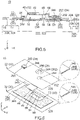
Fig. 5 is a schematic, cross-sectional view showing the device ofFig. 1 , taken along line V-V, wherein an inner structure of the device is merely schematically illustrated, and the size and arrangement of each member are not equal to the actual size and arrangement thereof. -
Fig. 6 is an exploded, perspective view showing the device ofFig. 1 , wherein a part of the first film enclosed by dashed line and a part of a second film enclosed by dashed line are enlarged and illustrated. -
Fig. 7 is a perspective view showing the air valve ofFig. 6 , wherein valves of the air valve are open. -
Fig. 8 is a side view showing the device ofFig. 1 , wherein the device is under manufacturing process. -
Fig. 9 is a schematic, cross-sectional view showing the device ofFig. 1 , taken along line V-V, wherein the device is under manufacturing process, the inner structure of the device is merely schematically illustrated, the size and arrangement of each member are not equal to the actual size and arrangement thereof, and a side surface of an instrument for vacuuming is illustrated. -
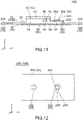
Fig. 10 is a cross-sectional view showing a modification of the device ofFig. 5 , wherein an inner structure of the device is merely schematically illustrated, and the size and arrangement of each member are not equal to the actual size and arrangement thereof. -
Fig. 11 is a cross-sectional view showing another modification of the device ofFig. 5 , wherein an inner structure of the device is merely schematically illustrated, and the size and arrangement of each member are not equal to the actual size and arrangement thereof. -
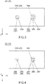
Fig. 12 is a top view showing a first sealing member of the device ofFig. 11 , wherein a hidden outline of a sub-member is illustrated with dashed line. -
Fig. 13 is a bottom view showing the first sealing member ofFig. 12 , wherein an outline of a hidden main opening of a first film and an outline of the hidden air valve are illustrated with dashed line. -
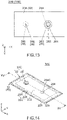
Fig. 14 is a perspective view showing a modification of the device ofFig. 1 , wherein boundary lines of a contact region formed between a first sealing member and a second sealing member are illustrated with dashed line. -
Fig. 15 is a schematic, cross-sectional view showing the device ofFig. 14 , taken along line XV-XV, wherein an inner structure of the device is merely schematically illustrated, and the size and arrangement of each member are not equal to the actual size and arrangement thereof. -
Fig. 16 is a perspective view showing another modification of the device ofFig. 1 , wherein an outline of a hidden main opening of a first film and boundary lines of a contact region formed between a first sealing member and a second sealing member are illustrated with dashed line. -
Fig. 17 is a cross-sectional view showing a device of Patent Document 1. - While the invention is susceptible to various modifications and alternative forms, specific embodiments thereof are shown by way of example in the drawings and will herein be described in detail. It should be understood, however, that the drawings and detailed description thereto are not intended to limit the invention to the particular form disclosed, but on the contrary, the intention is to cover all modifications, equivalents and alternatives falling within the spirit and scope of the present invention as defined by the appended claims.
- Referring to
Fig. 1 , adevice 10 according to an embodiment of the present invention is an independent electronic device. More specifically, thedevice 10 can work solely without another electronic device (not shown) physically attached thereto. For example, thedevice 10 measures the heart rate of a subject by attaching thedevice 10 near the heart of the subject and transmits the measurement result to another electronic device. Thus, thedevice 10 can be used as an electronic device for measuring biological information such as heart rate. However, the present invention is not limited thereto but is applicable to various devices having various functions. - Referring to
Fig. 2 together withFig. 1 , thedevice 10 of the present embodiment comprises acircuit structure 12 and a sealingmember 14. Thecircuit structure 12 is a member for enabling thedevice 10 to work as an electronic device. For example, thecircuit structure 12 has an electronic circuit (not shown) for receiving electric signals (hereafter, referred to as "biological signals") generated from electric pulse of the heart of the subject, another electronic circuit (not shown) for measuring the electric pulse of the heart based on the received biological signals and still another electronic circuit (not shown) for transmitting the measurement result to another electronic device (not shown). The sealingmember 14 entirely accommodates thecircuit structure 12 therewithin and protects thecircuit structure 12 from an external environment. Thus, thecircuit structure 12 is shut in the sealingmember 14. - The
circuit structure 12 of the present embodiment comprises afirst circuit member 40 and asecond circuit member 50. The sealingmember 14 of the present embodiment comprises a first sealingmember 20 and asecond sealing member 30. Thus, thedevice 10 comprises the first sealingmember 20, the second sealingmember 30, thefirst circuit member 40 and thesecond circuit member 50. Referring toFig. 8 together withFigs. 1 and 2 , the four members of thedevice 10, i.e., the first sealingmember 20, the second sealingmember 30, thefirst circuit member 40 and thesecond circuit member 50, are stacked in an upper-lower direction (Z-direction) and are combined to form thedevice 10 as a single structure. Thedevice 10 of the present embodiment comprises only the aforementioned four members. However, the present invention is not limited thereto, but thedevice 10 may further comprise another member in addition to the aforementioned four members. - Hereafter, explanation will be made about each member of the
device 10 of the present embodiment. - Referring to
Fig. 6 , the first sealingmember 20 of the present embodiment is formed of, as a base thereof, afirst film 22 which is an insulation film. In other words, the first sealingmember 20 comprises, as a base of the first sealingmember 20, thefirst film 22 formed of a film. Thefirst film 22 of the present embodiment is a thin, rectangular sheet and is bendable. For example, thefirst film 22 has a thickness of about 0.01 to 0.5 mm. Thefirst film 22 extends in parallel to a horizontal plane (sheet plane: XY-plane). Thefirst film 22 has aperipheral edge 229 in the XY-plane. - Referring to
Figs. 3 and 4 , thefirst film 22 has anouter surface 232 and aninner surface 234. Theouter surface 232 is an upper surface (positive Z-side surface) of thefirst film 22. Theinner surface 234 is a lower surface (negative Z-side surface) of thefirst film 22. - Referring to
Fig. 6 , thefirst film 22 of the present embodiment comprises two layers consisting of ameltable layer 146 which is meltable by heat-treatment and anunmeltable layer 148 which is not meltable by heat-treatment. Themeltable layer 146 is located under theunmeltable layer 148. For example, themeltable layer 146 is made of polyethylene, and theunmeltable layer 148 is made of nylon. According to this structure, themeltable layer 146 can be fused to another meltable layer of another member while theunmeltable layer 148 is maintained. However, the present invention is not limited thereto. For example, thefirst film 22 may comprise only one layer which is theunmeltable layer 148 or may comprise three or more layers. - The
first film 22 is formed with amain opening 244 and avalve opening 248. Each of themain opening 244 and thevalve opening 248 of the present embodiment has a small circular shape in the XY-plane and passes through thefirst film 22 in the Z-direction. For example, themain opening 244 has a diameter of 0.5 mm or less. Each of themain opening 244 and thevalve opening 248 as described above can be formed by a forming method such as laser irradiation. However, the present invention is not limited thereto. For example, the shape and the size in the XY-plane of each of themain opening 244 and thevalve opening 248 are not specifically limited. - Referring to
Figs. 1 and6 , the first sealingmember 20 of the present embodiment comprises a sub-member 26 and anair valve 28 in addition to thefirst film 22. - The sub-member 26 of the present embodiment is a circular, thin sheet and is bendable. The sub-member 26 comprises a thin
bondable portion 262 made of resin such as polyethylene terephthalate (PET) or polyurethane (PU) and a thinconductive portion 266 made of conductor such as metal. Thus, the first sealingmember 20 comprises thebondable portion 262 formed of a film and the thin film-likeconductive portion 266. - For example, each of the
bondable portion 262 and theconductive portion 266 of the present embodiment has a thickness of about 0.01 to 0.5 mm. The sub-member 26 is formed with a sub-opening 264. The sub-opening 264 has a small circular shape in the XY-plane. For example, the sub-opening 264 has a diameter of 0.5 mm or less. The sub-opening 264 passes through thebondable portion 262 in the Z-direction. However, the sub-opening 264 is filled with theconductive portion 266 so that no gap is left. In other words, theconductive portion 266 extends over the whole sub-opening 264 in the XY-plane and shuts the sub-opening 264. Theconductive portion 266 is exposed upward and downward. In other words, the positive Z-side surface and the negative Z-side surface of theconductive portion 266 are exposed outward. Thus, the sub-member 26 is formed so as to be electrically connectable in the Z-direction. - For example, the
sub-member 26 of the present embodiment can be formed as described below. First, a film having a thickness of about 0.01 to 0.5 mm is formed of resin such as PET or PU. Then, the film is formed with the sub-opening 264 having a diameter of 0.5 mm or less by a forming method such as laser irradiation. As a result, thebondable portion 262 is formed. Then, the sub-opening 264 is filled with conductive paste which is spread on one of opposite surfaces of the film by using a proper mask and a doctor blade. Then, the film is heated so that the conductive paste is hardened. Then, the sub-opening 264 is filled with conductive paste which is spread on a remaining one of the opposite surfaces of the film by using a proper mask and the doctor blade. Then, the film is heated so that the conductive paste is hardened. Theconductive portion 266 is formed of the conductive paste as a result of the aforementioned twice heat-treatment. - The sub-member 26 of the present embodiment is formed as described above and has the aforementioned structure. However, the present invention is not limited thereto. For example, the
conductive portion 266 may be formed by plating or by ink-jetting. Theconductive portion 266 may be formed of metal foil which is laminated on an upper or lower surface of thebondable portion 262 so as to cover thewhole sub-opening 264. Theconductive portion 266 may partially protrude downward. Moreover, the shape and the size of the sub-member 26 are not specifically limited. - In the present embodiment, the diameter of the
main opening 244 of thefirst film 22 is smaller than the diameter of thebondable portion 262 of the sub-member 26 but is larger than the diameter of theconductive portion 266 of the sub-member 26. Thebondable portion 262 of the present embodiment is bonded on theouter surface 232 so as to surround themain opening 244 in the XY-plane. In other words, a part of thebondable portion 262 which is located around the sub-opening 264 is bonded to thefirst film 22 throughout its entire circumference so as to surround themain opening 244. Thebondable portion 262 is firmly attached to theouter surface 232 and seals the edge of themain opening 244 in the XY-plane throughout its entire circumference. Thus, the sub-member 26 entirely shuts themain opening 244 and blocks air which might flow through themain opening 244. - The
bondable portion 262 of the present embodiment is bonded on theouter surface 232 of thefirst film 22 by using a fixing member such as an adhesive. However, the present invention is not limited thereto. For example, referring toFig. 6 , thefirst film 22 may further comprises another meltable layer (not shown) which is located over theunmeltable layer 148. Thebondable portion 262 may comprise a meltable layer (not shown) and an unmeltable layer (not shown). The meltable layer of thebondable portion 262 may be a lower layer of thebondable portion 262. According to the aforementioned modification, thebondable portion 262 can be bonded on theouter surface 232 of thefirst film 22 by fusing the meltable layer of thebondable portion 262 and the meltable layer of thefirst film 22 to each other. - Referring to
Figs. 3 and 4 , thebondable portion 262 of the present embodiment has an outer edge in the XY-plane which is located outward of themain opening 244 in the XY-plane. Moreover, thebondable portion 262 has an inner edge in the XY-plane which is located inward of themain opening 244 in the XY-plane. Thus, theconductive portion 266 of the present embodiment is located inward of themain opening 244 in the XY-plane. The thus-arrangedconductive portion 266 is vertically movable while thebondable portion 262 is resiliently deformed partially. In particular, when thebondable portion 262 is made of PU, thebondable portion 262 is resiliently deformable easily. However, the present invention is not limited thereto. For example, relationship in size in the XY-plane among thebondable portion 262, themain opening 244 and theconductive portion 266 can be variously modified as necessary. - Referring to
Figs. 6 and7 , theair valve 28 of the present embodiment comprises acover portion 282 formed of a thin insulation film and abase portion 286 made of insulator. As shown inFig. 7 , thebase portion 286 is formed with a passinghole 288. The passinghole 288 passes through thebase portion 286 in the Z-direction. Thecover portion 282 is formed with fivevalves 284 and fivecuts 285 which correspond to thevalves 284, respectively. Each of thecuts 285 passes through thecover portion 282 in the Z-direction. Thevalves 284 and thecuts 285 are located inward of an outer circumference of thecover portion 282 in the XY-plane. - Referring to
Fig. 7 together withFig. 6 , thecover portion 282 is adhered to and fixed on an upper surface of thebase portion 286. In particular, the outer circumference of thecover portion 282 in the XY-plane is tightly adhered to the upper surface of thebase portion 286 throughout its entire circumference. In contrast, an inner part of thecover portion 282, which is located inward of the outer circumference of thecover portion 282 in the XY-plane, can be pulled away from the upper surface of thebase portion 286. Thus, a passage which allows air to pass therethrough can be formed between the passinghole 288 and each of thecuts 285. Thebase portion 286 has a lower surface which is adhered to and fixed on thefirst film 22 in such a way that the passinghole 288 communicates with thevalve opening 248 of thefirst film 22. - Referring to
Fig. 1 together withFig. 7 , theair valve 28 can take either an open state shown inFig. 7 or a closed state shown inFig.1 . When theair valve 28 takes the open state, each of thevalves 284 is apart from thecorresponding cut 285. When theair valve 28 takes the closed state, each of thevalves 284 completely covers thecorresponding cut 285. When theair valve 28 takes the open state, an air passage via theair valve 28 is formed between the inside and the outside of thedevice 10. When theair valve 28 takes the closed state, the inside of thedevice 10 is shut off from the outside of thedevice 10. - As described later, the
air valve 28 is used for vacuuming the inside of thedevice 10 upon fabrication of thedevice 10. Theair valve 28 of the present embodiment has a structure suitable for this use. However, the present invention is not limited thereto. For example, the structure of theair valve 28 is not specifically limited, provided that the inside air of thedevice 10 can be discharged by using theair valve 28. Moreover, the inside of thedevice 10 may be vacuumed without provision of theair valve 28. In other words, theair valve 28 may be provided as necessary. - Referring to
Fig. 6 , the second sealingmember 30 of the present embodiment is formed of, as a base thereof, asecond film 32 which is an insulation film. In other words, the second sealingmember 30 comprises, as a base of the second sealingmember 30, thesecond film 32 formed of a film. Thesecond film 32 of the present embodiment is formed of material similar to that of thefirst film 22 and has a structure similar to that of thefirst film 22. For example, thesecond film 32 is a thin, rectangular sheet and is bendable. Thesecond film 32 extends in parallel to the XY-plane. Thesecond film 32 has aperipheral edge 329 in the XY-plane. However, the present invention is not limited thereto. For example, the second sealingmember 30 may comprise, as a base thereof, a rigid circuit board instead of thesecond film 32. The rigid circuit board may have rigidity and may be hardly bent. - The
second film 32 or the rigid circuit board of the present embodiment comprises, similarly to thefirst film 22, two layers consisting of themeltable layer 146 which is meltable by heat-treatment and theunmeltable layer 148 which is not meltable by heat-treatment. Themeltable layer 146 is located over theunmeltable layer 148. According to this structure, the twomeltable layers 146 of thefirst film 22 and thesecond film 32 can be fused to each other while theunmeltable layers 148 are maintained. However, the present invention is not limited thereto. Each of thefirst film 22 and thesecond film 32 may have any structure, provided that it is in accordance with a forming method of thedevice 10. For example, thefirst film 22 and thesecond film 32 may be bonded together by using a fixing member such as an adhesive. In this instance, each of thefirst film 22 and thesecond film 32 may comprise only one layer which is theunmeltable layer 148. Instead, each of thefirst film 22 and thesecond film 32 may comprise three or more layers. - Referring to
Figs. 2 and6 , the second sealingmember 30 of the present embodiment comprises anadditional film 38 formed of an insulation film in addition to thesecond film 32. Theadditional film 38 has anuneven portion 382. As described later, theuneven portion 382 is provided in order to maintain a passage which allows air to pass therethrough upon vacuuming the inside of thedevice 10. In detail, theuneven portion 382 is formed with a large number ofprojections 384. Each of theprojections 384 is a projection which projects upward and is resiliently deformable. Theprojections 384 are uniformly and continuously formed over the entireadditional film 38 in the XY-plane. According to the structure described above, a passage which allows air to pass therethrough is formed between every adjacent two of theprojections 384. The shape and the size of each of theprojections 384 are not specifically limited, provided that the passage which allows air to pass therethrough can be formed. - Referring to
Fig. 1 together withFig. 2 , thefirst film 22 and thesecond film 32 of the present embodiment overlap with each other so that the position of theperipheral edge 229 and the position of theperipheral edge 329 are aligned with each other in the XY-plane. However, the present invention is not limited thereto. For example, the size of thefirst film 22 in the XY-plane and the size of thesecond film 32 in the XY-plane may be different from each other. The shape of each of thefirst film 22 and thesecond film 32 is not limited to be rectangular but can be modified as necessary. - Referring to
Fig. 6 , thefirst circuit member 40 of the present embodiment has afirst base portion 42 and a firstconductive pattern 44. Thefirst base portion 42 of the present embodiment is a thin, rectangular sheet formed of an insulation film and is bendable. Thefirst base portion 42 extends in parallel to the XY-plane. The firstconductive pattern 44 is formed on thefirst base portion 42. In detail, the firstconductive pattern 44 is made of conductor such as copper and is formed on a lower surface of thefirst base portion 42 by a forming method such as silver ink printing or etching. - The
second circuit member 50 of the present embodiment has asecond base portion 52 and a secondconductive pattern 54. Thesecond base portion 52 of the present embodiment is a thin, rectangular sheet formed of an insulation film and is bendable. Thesecond base portion 52 extends in parallel to the XY-plane. The secondconductive pattern 54 is formed on thesecond base portion 52. In detail, the secondconductive pattern 54 is made of conductor such as copper and is formed on an upper surface of thesecond base portion 52 by a forming method such as silver ink printing or etching. - Each of the
first circuit member 40 and thesecond circuit member 50 of the present embodiment has the aforementioned structure. However, the present invention is not limited thereto. For example, each of thefirst circuit member 40 and thesecond circuit member 50 may be provided with one or more electronic components. One of thefirst circuit member 40 and thesecond circuit member 50 may be a single electronic component. Each of thefirst circuit member 40 and thesecond circuit member 50 may be a rigid circuit board. The forming method of each of the firstconductive pattern 44 and the secondconductive pattern 54 is not specifically limited, provided that each of the firstconductive pattern 44 and the secondconductive pattern 54 is made of conductor. - The first
conductive pattern 44 of the present embodiment has afirst contact point 48. The secondconductive pattern 54 of the present embodiment has asecond contact point 58 and anelectrode 59. Thus, thefirst circuit member 40 comprises thefirst contact point 48, and thesecond circuit member 50 comprises thesecond contact point 58 and theelectrode 59. Referring toFigs. 2 and5 , thefirst contact point 48 and thesecond contact point 58 are in contact with each other in the fabricateddevice 10. Referring toFig. 5 , theelectrode 59 and theconductive portion 266 are in contact with each other in the fabricateddevice 10. Thus, the firstconductive pattern 44 and the secondconductive pattern 54 are electrically connected with each other and are electrically connectable with a member located outside thedevice 10 through theconductive portion 266. - The first
conductive pattern 44 and the secondconductive pattern 54 illustrated inFig. 6 are abstract conductive patterns for simple explanation about the present invention and have no specific function. In other words, even when the illustratedfirst contact point 48 and the illustratedsecond contact point 58 are brought into contact with each other, thedevice 10 does not work as an electronic device. For example, the actual firstconductive pattern 44 and the actual secondconductive pattern 54 are formed with an electronic circuit (not shown) which can measure the electric pulse of the heart of the subject. Referring toFig. 1 , this electronic circuit can obtain biological signals based on the electric pulse of the heart of the subject via theconductive portion 266. - Referring to
Fig. 2 , each of the number of thefirst contact point 48 and the number of thesecond contact point 58 of the present embodiment is one. Moreover, each of the number of theelectrode 59 and the number of theconductive portion 266 is one. However, the present invention is not limited thereto. For example, each of the number of the first contact points 48 and the number of the second contact points 58 may be two or more. Moreover, each of the number of theelectrodes 59 and the number of theconductive portions 266 may be two or more. In the fabricateddevice 10, the first contact points 48 should be in contact with the second contact points 58, respectively, and theelectrodes 59 should be in contact with theconductive portions 266, respectively. - Hereafter, more specific explanation will be made about the
device 10 of the present embodiment. - Referring to
Figs. 1 and 2 , thefirst film 22 of the present embodiment has a firstinner portion 222 and a firstouter portion 224. The firstouter portion 224 of the present embodiment has afirst seal portion 226 and afirst contact portion 228. The firstinner portion 222 is located inward of the firstouter portion 224 in the XY-plane. In other words, the firstouter portion 224 is a part of thefirst film 22 which surrounds the firstinner portion 222. - Referring to
Fig. 2 , thesecond film 32 of the present embodiment has a secondinner portion 322 and a secondouter portion 324. The secondouter portion 324 of the present embodiment has asecond seal portion 326 and asecond contact portion 328. The secondinner portion 322 is located inward of the secondouter portion 324 in the XY-plane. In other words, the secondouter portion 324 is a part of thesecond film 32 which surrounds the secondinner portion 322. - Referring to
Figs. 1 and 2 , the firstinner portion 222 of thefirst film 22 and the secondinner portion 322 of thesecond film 32 of thedevice 10 are parts for accommodating thecircuit structure 12 and are apart from each other. Thefirst seal portion 226 and thesecond seal portion 326 of the present embodiment are bonded together to form aseal trace 16. According to the present embodiment, thefirst seal portion 226 and thesecond seal portion 326 are bonded together by heat-sealing. Thus, theseal trace 16 of the present embodiment is a trace where thefirst seal portion 226 and thesecond seal portion 326 are welded to each other by heat-treatment. However, the present invention is not limited thereto, but thefirst seal portion 226 and thesecond seal portion 326 can be bonded together by various methods such as high frequency, ultrasonic, laser or adhesive. - The
seal trace 16 of the present embodiment is formed throughout entire circumference of thefirst seal portion 226 and thesecond seal portion 326. Theseal trace 16 surrounds thefirst contact portion 228 and thesecond contact portion 328 throughout their entire circumference in the XY-plane. However, the present invention is not limited thereto, but theseal trace 16 may be formed on a necessary part in accordance with the forming method of thedevice 10. For example, theseal trace 16 may be partially formed or may not be formed at all. - Referring to
Fig. 5 , as described later, the inside of thedevice 10 is vacuumed after thefirst seal portion 226 and thesecond seal portion 326 are bonded together. According to the present embodiment, upon vacuuming, thefirst contact portion 228 and thesecond contact portion 328 are brought into contact with each other in acontact region 17 because of air pressure difference. As a result, thedevice 10 is formed with aclosed space 18. Theclosed space 18 is enclosed by the firstinner portion 222 and the secondinner portion 322. Thecontact region 17 of the present embodiment seamlessly surrounds the firstinner portion 222 and the secondinner portion 322 throughout their entire circumference in the XY-plane. However, the present invention is not limited thereto, but thecontact region 17 may be formed on a necessary part in accordance with the forming method of thedevice 10. For example, thecontact region 17 may be partially formed or may not be formed at all. - The
closed space 18, which is formed as described above, is enclosed by the first sealingmember 20 and the second sealingmember 30 and is shut off from an outer space outside thedevice 10. According to the present embodiment, thefirst seal portion 226 and thesecond seal portion 326 are firmly bonded together. In addition, thecontact region 17 is located inward of theseal trace 16 in the XY-plane and blocks air which might flow between the inside and the outside of the closedspace 18. Thus, air pressure in the closedspace 18 is kept to low pressure lower than the atmospheric pressure. - The
first circuit member 40 and thesecond circuit member 50 are shut in the closedspace 18 which is kept to the aforementioned low pressure. Thefirst contact point 48 and thesecond contact point 58 are pressed against each other to be in contact with each other in the closedspace 18. In detail, a contact force is generated between thefirst contact point 48 and thesecond contact point 58 because of air pressure difference between the inside and the outside of the closedspace 18. Thefirst contact point 48 and thesecond contact point 58 are pressed against each other because of this air pressure difference. Therefore, the contact between thefirst contact point 48 and thesecond contact point 58 can be securely kept. - Summarizing the explanation described above, the first sealing
member 20 and the second sealingmember 30 of thedevice 10 of the present embodiment overlap with each other to be in contact with each other while thefirst circuit member 40 and the second circuit member 50 (hereafter, simply referred to as "circuit members") are sandwiched therebetween. Each of the first sealingmember 20 and the second sealingmember 30 of the present embodiment is basically formed of a film. - Moreover, the structure of each of the circuit members is not restricted except that the circuit members should be provided with the
electrode 59 and the contact points consisting of thefirst contact point 48 and thesecond contact point 58. Thus, each of the circuit members of the present embodiment has a simple structure and can be formed of various material. For example, the circuit members may be two insulation films formed with the conductive patterns consisting of the firstconductive pattern 44 and the secondconductive pattern 54. The conductive patterns may merely have the contact points and theelectrode 59. In this instance, the thickness of theentire device 10 can be made extremely thin. Thus, the present embodiment provides thedevice 10 which is new and can be made thinner. - According to the present embodiment, the
first seal portion 226 and thesecond seal portion 326 are bonded together, and thefirst contact portion 228 and thesecond contact portion 328 are in contact with each other. According to this structure, the closedspace 18 can be reliably kept airtight. However, the present invention is not limited to the present embodiment. For example, thefirst seal portion 226 and thesecond seal portion 326 may partially surround thefirst contact portion 228 and thesecond contact portion 328 in the XY-plane. Thefirst seal portion 226 and thesecond seal portion 326 may partially surround the firstinner portion 222 and the secondinner portion 322 in the XY-plane. - According to the present embodiment, the
first circuit member 40 and thesecond circuit member 50 can be easily taken out from the closedspace 18 by cutting off thefirst seal portion 226 and thesecond seal portion 326. Thus, according to the present embodiment, the members can be easily collected separately and can be reused. - The
conductive portion 266 of the present embodiment is in contact with theelectrode 59 in the closedspace 18 and is partially exposed to the outer space located outside thedevice 10. In detail, theouter surface 232 of thefirst film 22 is located outside theclosed space 18. Thebondable portion 262 of the sub-member 26 is bonded on the thus-arrangedouter surface 232. Theconductive portion 266 and theelectrode 59 are pressed against each other because of air pressure difference between the inside and the outside of the closedspace 18 so that the contact between theconductive portion 266 and theelectrode 59 can be reliably kept. - If the
conductive portion 266 as described above is not provided, electronic circuits (not shown) formed in the firstconductive pattern 44 and the secondconductive pattern 54 should obtain biological signals of a subject with no contact with the subject. For example, the electronic circuits should obtain biological signals of the subject by contactless communication. However, weak biological signals are difficult to be accurately obtained by contactless communication. In contrast, according to the present embodiment, biological signals can be accurately obtained via theconductive portion 266 which is in contact with a skin of the subject. - Each of the first sealing
member 20 and the second sealingmember 30 is preferred to have a high barrier property against oxygen. More specifically, each of thefirst film 22 and the second film 32 (or rigid circuit board) is preferred to comprise a layer made of high oxygen barrier material which is material having a high barrier property against oxygen. According to this layer-structure, oxidation of the metal members of thecircuit structure 12 can be reduced. - For example, the high oxygen barrier material may be linear low-density polyethylene (LLDPE). More specifically, the high oxygen barrier material may be PET/AI/PE which is formed by laminating polyethylene terephthalate, aluminum and polyethylene; ON/PE which is formed by laminating biaxially stretched nylon and polyethylene; PET/EVOH/PE which is formed by laminating polyethylene terephthalate, polyvinyl chloride and polyethylene; or may be formed by laminating a transparent high barrier film and polyethylene. The transparent high barrier film may be polyethylene terephthalate (PET) deposited with SiOx or aluminum oxide.
- Each of the first sealing
member 20 and the second sealingmember 30 of the present embodiment is preferred to have a high barrier property against water vapor in addition to the high barrier property against oxygen. More specifically, each of thefirst film 22 and the second film 32 (or rigid circuit board) is preferred to comprise a layer made of high water-vapor barrier material which is material having a high barrier property against water vapor. According to this layer-structure, thecircuit structure 12 can be water-proofed. For example, the high water-vapor barrier material may be material which is a sheet made of ON/PE, biaxially stretched polypropylene (OPP) or PET and is coated with polyvinylidene chloride (PVDC). - Each of the first sealing
member 20 and the second sealingmember 30 may have various barrier properties such as a barrier property against nitrogen in addition to the high barrier property against oxygen and the high barrier property against water vapor. Thus, each of the first sealingmember 20 and the second sealingmember 30 is preferred to have high barrier properties in accordance with its use. - The device 10 (see
Fig. 1 ) of the present embodiment is formed via four steps consisting of a preparing step (STEP 1), a stacking step (STEP 2), a shutting-in step (STEP 3) and a vacuuming step (STEP 4). However, the present invention is not limited thereto, but the forming method of thedevice 10 can be modified as necessary. Hereafter, explanation will be made about an example of the forming method of thedevice 10 of the present embodiment. - Referring to
Fig. 8 , first, in the preparing step, the first sealingmember 20, the second sealingmember 30, thefirst circuit member 40 and thesecond circuit member 50 are prepared. - Then, in the stacking step, the first sealing
member 20, thefirst circuit member 40, thesecond circuit member 50 and the second sealingmember 30 are stacked on each other in this order from top to bottom along the Z-direction. Meanwhile, thefirst circuit member 40 and thesecond circuit member 50 are arranged so that thefirst contact point 48 and thesecond contact point 58 face each other in the Z-direction. Moreover, theconductive portion 266 and theelectrode 59 are arranged so as to face each other in the Z-direction. Theadditional film 38 is located at the middle ofsecond film 32 in the XY-plane. Thefirst circuit member 40 and thesecond circuit member 50 are located at the middle of theadditional film 38 in the XY-plane. In addition, thefirst film 22 and thesecond film 32 are arranged so that two of the meltable layers 146 (seeFig. 6 ) thereof face each other in the Z-direction. - Then, in the shutting-in step, heat-sealing is applied to the
first film 22 and thesecond film 32. In detail, parts of the twomeltable layers 146, which are located at outer circumferences of thefirst film 22 and thesecond film 32 in the XY-plane, are welded to each other via heat-sealing. Referring toFig. 9 , as a result of the heat-sealing, thedevice 10 with theseal trace 16 is formed. Thedevice 10 has an inner space which is enclosed by the first sealingmember 20 and the second sealingmember 30 and which is shut off from the outside of thedevice 10 except for theair valve 28. - Then, in the vacuuming step, the inside of the
device 10 is vacuumed. According to the present embodiment, theair valve 28 and aninstrument 80 are used to discharge the air of the inside of thedevice 10. Theinstrument 80 of the present embodiment is a syringe-type piston pump. Theinstrument 80 comprises asyringe 82 and aplunger 84. Thesyringe 82 has a lower end which has a ring shape in the XY-plane. The ring shape of thesyringe 82 corresponds to the outer circumference of thecover portion 282 of theair valve 28. - In the vacuuming step, first, the lower end of the
syringe 82 is pressed against the upper surface of thecover portion 282. Then, theplunger 84 is pulled upward. Meanwhile, theair valve 28 takes the open state, and an air passage is formed between the inside of thedevice 10 and the inside of thesyringe 82. The air in the inside of thedevice 10 is discharged into the inside of thesyringe 82 through the passinghole 288 and the cuts 285 (seeFig. 7 ) of theair valve 28. As a result, air pressure of the inside of thedevice 10 is gradually lowered. When air pressure of the inside of thedevice 10 becomes low pressure close to that of a vacuum, the vacuuming by using theinstrument 80 is stopped. - Referring to
Fig. 5 together withFig. 9 , when the vacuuming is stopped, the valves 284 (seeFig. 7 ) of theair valve 28 cover the cuts 285 (seeFig. 7 ) because of air pressure difference between air pressure of the inside of thedevice 10 and the atmospheric pressure, and thereby theair valve 28 takes the closed state. As a result, air pressure of the inside of thedevice 10 is kept to low pressure. Thus, thedevice 10 is formed with the closedspace 18 which is shut off from the outside and has the low pressure. Thefirst contact point 48 and thesecond contact point 58 are pressed against each other and are brought into contact with each other because of air pressure difference between the inside and the outside of the closedspace 18. Theconductive portion 266 and theelectrode 59 are pressed against each other and are brought into contact with each other because of the air pressure difference between the inside and the outside of the closedspace 18. - The
first film 22 and thesecond film 32 tend to be in close contact with each other upon vacuuming, and thereby tend to form a close contact part such as thecontact region 17. If theadditional film 38 is not provided, the close contact part of thefirst film 22 and thesecond film 32 will be formed in the closedspace 18. The thus-formed close contact part might block an air passage between theair valve 28 and a contact point region where thefirst contact point 48 and thesecond contact point 58 are arranged. As a result, air pressure of a space in which thefirst contact point 48 and thesecond contact point 58 are located might be insufficiently lowered, and thereby thefirst contact point 48 and thesecond contact point 58 might be unreliably brought into contact with each other. Similarly, theconductive portion 266 and theelectrode 59 might be unreliably brought into contact with each other. - In contrast, since the
additional film 38 of the present embodiment is located between thefirst film 22 and thesecond film 32, direct contact between thefirst film 22 and thesecond film 32 is prevented. Moreover, since theadditional film 38 has theuneven portion 382, the air passage through theair valve 28 can be kept even in a case where thefirst film 22 and thesecond film 32 are indirectly brought into contact with each other via theadditional film 38. Therefore, thefirst contact point 48 and thesecond contact point 58 can be reliably brought into contact with each other. Similarly, theconductive portion 266 and theelectrode 59 can be reliably brought into contact with each other. - The
additional film 38 of the present embodiment is an embossed film distinct and separable from thesecond film 32 and is arranged on thesecond film 32. Theuneven portion 382 is formed over upper and lower surfaces of theadditional film 38. However, the present invention is not limited thereto. For example, theadditional film 38 may be adhered to and fixed on an upper surface of thesecond film 32. Theuneven portion 382 may be formed only on the upper surface of theadditional film 38. Thesecond film 32 may be embossed so as to be formed with theuneven portion 382. In this instance, theadditional film 38 does not need to be provided. Thus, the second sealingmember 30 may comprise only thesecond film 32 which has theuneven portion 382. - The
additional film 38 of the present embodiment forms the second sealingmember 30 together with thesecond film 32. However, the present invention is not limited thereto. For example, theadditional film 38 may form the first sealingmember 20 together with thefirst film 22. More specifically, theadditional film 38 may be arranged under thefirst film 22. Moreover, thefirst film 22 may be embossed so as to be formed with theuneven portion 382. In this instance, theadditional film 38 does not need to be provided. - According to the forming method of the present embodiment, the
first contact point 48 and thesecond contact point 58 are securely in contact with each other without using a fixing member such as an adhesive. Theconductive portion 266 and theelectrode 59 are securely in contact with each other without using a fixing member such as an adhesive. Therefore, when thedevice 10 is no longer used, thedevice 10 can be disassembled merely by cutting off the firstouter portion 224 and the secondouter portion 324. In addition, thefirst circuit member 40 and thesecond circuit member 50 can be shut in the closedspace 18 having low pressure, and thereby degradation of the metal members due to oxidation can be reduced, for example. - Referring to
Fig. 9 , according to the forming method of the present embodiment, thesimple instrument 80 can be used for easy vacuuming. The vacuuming by theinstrument 80 can be repeatedly performed. For example, even when air pressure in the closedspace 18 becomes higher during use of thedevice 10, theinstrument 80 can be used for vacuuming again. Thus, during use of thedevice 10, the contact force between thefirst contact point 48 and thesecond contact point 58 can be kept, and the contact force between theconductive portion 266 and theelectrode 59 can be kept. However, the present invention is not limited thereto, but the forming method of thedevice 10 can be modified as necessary. - For example, the structure of the
instrument 80 is not specifically limited, provided that it can be used for vacuuming. A nozzle may be used instead of the illustratedinstrument 80. The nozzle may be inserted into and vacuum thedevice 10. In this instance, theair valve 28 does not need to be provided. Alternatively, a commercially available desktop vacuum packaging machine (not shown) may be used for sealing and vacuuming. Referring toFig. 8 , the members of thedevice 10 may be arranged in a chamber (not shown) so that vacuuming is performed simultaneously with heat-sealing. According to this forming method, theadditional film 38 does not need to be provided. In addition, the other member does not need to be provided with theuneven portion 382. However, a commercially available, simple instrument such as the instrument 80 (seeFig. 9 ) is preferable from a viewpoint of easy fabrication of thedevice 10. - According to the forming method of the present embodiment, the sub-member 26 has been bonded to the
first film 22 when the preparing step starts. However, the present invention is not limited thereto. For example, the sub-member 26 may be bonded to thefirst film 22 by fusing after the vacuuming step ends. However, the forming method of the present embodiment is preferable from a viewpoint of reliably vacuuming the inside of thedevice 10. - The present embodiment can be further variously modified as described below in addition to the already described modifications.
- Comparing
Fig. 10 withFig. 5 , adevice 10A according to a first modification comprises the second sealingmember 30 same as that of thedevice 10. Moreover, thedevice 10A comprises afirst sealing member 20A, afirst circuit member 40A and asecond circuit member 50A which are different from the first sealingmember 20, thefirst circuit member 40 and thesecond circuit member 50 of thedevice 10, respectively. - The
first sealing member 20A comprises afirst film 22A similar to thefirst film 22 and comprises the sub-member 26 and theair valve 28 same as those of the first sealingmember 20. Thefirst film 22A is formed with amain opening 244A similar to themain opening 244. Themain opening 244A is located above thefirst circuit member 40A. - The
second circuit member 50A has a structure similar to that of thesecond circuit member 50 except that theelectrode 59 is not provided. On the other hand, thefirst circuit member 40A comprises anelectrode 49A. In detail, thefirst circuit member 40A comprises afirst base portion 42A and a firstconductive pattern 44A. Thefirst base portion 42A is formed with a via hole which vertically passes through thefirst base portion 42A. Theelectrode 49A is formed on an upper surface of thefirst base portion 42A and is connected to the firstconductive pattern 44A, which is formed on a lower surface of thefirst base portion 42A, through the via hole. The sub-member 26 is bonded on theouter surface 232 of thefirst film 22A so as to shut themain opening 244A. Theconductive portion 266 of the sub-member 26 is in contact with theelectrode 49A the firstconductive pattern 44A instead of theelectrode 59 of the secondconductive pattern 54. - Except for the differences described above, the
device 10A has a structure similar to that of thedevice 10 and works similarly to thedevice 10. Thus, according to the present modification, the effect similar to that of the aforementioned embodiment can be obtained. - As can be seen from the explanation described above, the
first circuit member 40A may comprise theelectrode 49A, while thesecond circuit member 50 may comprise theelectrode 59. Instead, thefirst circuit member 40A may comprise theelectrode 49A, and thesecond circuit member 50 may comprise theelectrode 59. Thus, at least one of the first circuit member and the second circuit member should comprise an electrode configured to be connected to theconductive portion 266. - Comparing
Fig. 11 withFig. 5 , adevice 10B according to a second modification comprises the second sealingmember 30, thefirst circuit member 40 and thesecond circuit member 50 same as those of thedevice 10. Moreover, thedevice 10B comprises afirst sealing member 20B different from the first sealingmember 20 of thedevice 10. Thefirst sealing member 20B comprises thefirst film 22, the sub-member 26 and theair valve 28 same as those of the first sealingmember 20. Theinner surface 234 of thefirst film 22 is located inside the closedspace 18. Thebondable portion 262 of the sub-member 26 is bonded on the thus-arrangedinner surface 234 by using a fixing member such as an adhesive. - Except for the differences described above, the
device 10B has a structure similar to that of thedevice 10 and works similarly to thedevice 10. For example, referringFigs. 11 to 13 , a part of thebondable portion 262 which is located around the sub-opening 264 is bonded to thefirst film 22 throughout its entire circumference so as to surround themain opening 244. Theconductive portion 266 is in contact with theelectrode 59 in the closedspace 18 and is partially exposed to the outer space located outside thedevice 10. Theconductive portion 266 and theelectrode 59 are pressed against each other because of air pressure difference between the inside and the outside of the closedspace 18, and thereby the contact between theconductive portion 266 and theelectrode 59 can be securely kept. Thus, according to the present modification, the effect similar to that of the aforementioned embodiment and the first modification can be obtained. - The
bondable portion 262 of the present modification may comprise a meltable layer (not shown) and an unmeltable layer (not shown). The meltable layer of thebondable portion 262 may be an upper layer of thebondable portion 262. In this instance, thebondable portion 262 may be fused to the meltable layer 146 (seeFig. 6 ) of thefirst film 22. - Comparing
Figs. 14 and15 withFigs. 1 and5 , adevice 10C according to a third modification comprises the second sealingmember 30, thefirst circuit member 40 and thesecond circuit member 50 same as those of thedevice 10. Moreover, thedevice 10C comprises afirst sealing member 20C different from the first sealingmember 20 of thedevice 10. Thefirst sealing member 20C comprises thefirst film 22 and theair valve 28 same as those of the first sealingmember 20. However, thefirst sealing member 20C does not comprise the sub-member 26. Thefirst sealing member 20C comprises aconductive portion 246C instead of theconductive portion 266 of the sub-member 26. - The
conductive portion 246C is made of conductor such as metal similarly to theconductive portion 266 and is formed by a forming method similar to that of theconductive portion 266. Theconductive portion 246C shuts themain opening 244 of thefirst film 22. Theconductive portion 246C extends over the wholemain opening 244 in the XY-plane and entirely shuts themain opening 244. Thus, theconductive portion 246C blocks air which might flow through themain opening 244. - Except for the differences described above, the
device 10C has a structure similar to that of thedevice 10 and works similarly to thedevice 10. For example, referringFig. 15 , theconductive portion 246C is in contact with theelectrode 59 in the closedspace 18 and is partially exposed to the outer space located outside thedevice 10. Theconductive portion 246C and theelectrode 59 are pressed against each other because of air pressure difference between the inside and the outside of the closedspace 18, and thereby the contact between theconductive portion 246C and theelectrode 59 can be securely kept. Thus, according to the present modification, the effect similar to that of the aforementioned embodiment, the first modification and the second modification can be obtained. - The present embodiment can be further variously modified in addition to the already described modifications.
- For example, referring to
Fig. 6 , theperipheral edge 229 of thefirst film 22 and theperipheral edge 329 of thesecond film 32 may be connected to each other at a rear end (negative X-side end) thereof in a front-rear direction (X-direction). In other words, each of thefirst film 22 and thesecond film 32 may be a part of a single planar sheet which is folded so that thefirst film 22 and thesecond film 32 overlap with each other. Instead, theperipheral edge 229 of thefirst film 22 and theperipheral edge 329 of thesecond film 32 may be connected to each other except for the rear end thereof. In other words, each of thefirst film 22 and thesecond film 32 may be a part of a single folder-like sheet. - The aforementioned folder-like sheet may have an openable and closable fastener which is provided on a rear end part thereof. In this instance, vacuuming may be performed under a state where the fastener is closed. Thereafter, parts of the
first film 22 and thesecond film 32 which are located forward (positive X-side) of the fastener may be fused to each other. The part provided with theair valve 28 may be cut off after the fusing. - The
first circuit member 40 may be a member integral to the first sealingmember 20. Thesecond circuit member 50 may be a member integral to the second sealingmember 30. For example, thefirst base portion 42 may be adhered to and fixed on a lower surface of thefirst film 22. Instead, the firstconductive pattern 44 may be formed on the lower surface of thefirst film 22. Thesecond circuit member 50 may be provided on theadditional film 38. For example, thesecond base portion 52 may be adhered to and fixed on the upper surface of theadditional film 38. Instead, the secondconductive pattern 54 may be formed on the upper surface of theadditional film 38. Moreover, when the second sealingmember 30 does not comprise theadditional film 38, thesecond base portion 52 may be adhered to and fixed on the upper surface of thesecond film 32. Instead, the secondconductive pattern 54 may be formed on the upper surface of thesecond film 32. - Referring to
Fig. 16 together withFigs. 9 to 11 , as previously described, the forming method of theconductive portion 266 of the sub-member 26 is not specifically limited. For example, the sub-member 26 may be aconductive gel 26D. In other words, the first sealingmember conductive gel 26D (see thedevice 10D ofFig. 16 ) instead of the sub-member 26. Theconductive gel 26D has flexibility and adhesiveness as well as conductivity and is thereby suitable to be directly attached to a human body. When theconductive gel 26D is used, the sub-opening 264 does not need to be formed. A part of theconductive gel 26D which covers themain opening conductive portion 266, and another part of theconductive gel 26D which is configured to be bonded to thefirst film bondable portion 262. Thus, theconductive gel 26D comprises theconductive portion 266 and thebondable portion 262 similarly to the sub-member 26 and works similarly to the sub-member 26.
Claims (8)
- A device comprising a first sealing member, a second sealing member, a first circuit member and a second circuit member, wherein:the first sealing member comprises, as a base of the first sealing member, a first film formed of a film and comprises a conductive portion made of conductor;the device is formed with a closed space;the closed space is enclosed by the first sealing member and the second sealing member and is shut off from an outer space located outside the device;the first circuit member and the second circuit member are shut in the closed space;the first circuit member comprises a first contact point;the second circuit member comprises a second contact point;the first contact point and the second contact point are pressed against each other to be in contact with each other in the closed space;at least one of the first circuit member and the second circuit member comprises an electrode; andthe conductive portion is in contact with the electrode in the closed space and is partially exposed to the outer space located outside the device.
- The device as recited in claim 1, wherein:the first film is formed with a main openingthe main opening passes through the first film; andthe conductive portion shuts the main opening.
- The device as recited in claim 1, wherein:the first sealing member comprises a sub-member in addition to the first film;the first film is formed with a main opening;the main opening passes through the first film;the sub-member comprises a bondable portion and the conductive portion;the sub-member is formed with a sub-opening;the sub-opening passes through the bondable portion;the conductive portion shuts the sub-opening; anda part of the bondable portion which is located around the sub-opening is bonded to the first film throughout its entire circumference.
- The device as recited in claim 3, wherein:the first film has an outer surface;the outer surface is located outside the closed space; andthe bondable portion is bonded on the outer surface.
- The device as recited in claim 3, wherein:the first film has an inner surface;the inner surface is located inside the closed space; andthe bondable portion is bonded on the inner surface.
- The device as recited in one of claims 3 to 5, wherein the bondable portion of the sub-member is formed of a film.
- The device as recited in one of claims 1 to 6, wherein the second sealing member comprises, as a base of the second sealing member, a second film formed of a film.
- A device comprising a first sealing member, a second sealing member, a first circuit member and a second circuit member, wherein:the first sealing member comprises, as a base of the first sealing member, a first film formed of a film and comprises a conductive gel;the device is formed with a closed space;the closed space is enclosed by the first sealing member and the second sealing member and is shut off from an outer space located outside the device;the first circuit member and the second circuit member are shut in the closed space;the first circuit member comprises a first contact point;the second circuit member comprises a second contact point;the first contact point and the second contact point are pressed against each other to be in contact with each other in the closed space;at least one of the first circuit member and the second circuit member comprises an electrode;the conductive gel comprises a conductive portion; andthe conductive portion is in contact with the electrode in the closed space and is partially exposed to the outer space located outside the device.
Applications Claiming Priority (2)
| Application Number | Priority Date | Filing Date | Title |
|---|---|---|---|
| JP2021064367 | 2021-04-05 | ||
| JP2022008089A JP7822186B2 (en) | 2021-04-05 | 2022-01-21 | device |
Publications (2)
| Publication Number | Publication Date |
|---|---|
| EP4081003A1 true EP4081003A1 (en) | 2022-10-26 |
| EP4081003B1 EP4081003B1 (en) | 2024-09-04 |
Family
ID=80978809
Family Applications (1)
| Application Number | Title | Priority Date | Filing Date |
|---|---|---|---|
| EP22165018.7A Active EP4081003B1 (en) | 2021-04-05 | 2022-03-29 | Device comprising a circuit member sealed by a film |
Country Status (3)
| Country | Link |
|---|---|
| US (1) | US11800643B2 (en) |
| EP (1) | EP4081003B1 (en) |
| CN (1) | CN115206896B (en) |
Families Citing this family (2)
| Publication number | Priority date | Publication date | Assignee | Title |
|---|---|---|---|---|
| JP7638690B2 (en) * | 2020-12-11 | 2025-03-04 | 日本航空電子工業株式会社 | DEVICE AND METHOD FOR MANUFACTURING DEVICE - Patent application |
| JP7638767B2 (en) | 2021-04-05 | 2025-03-04 | 日本航空電子工業株式会社 | device |
Citations (4)
| Publication number | Priority date | Publication date | Assignee | Title |
|---|---|---|---|---|
| US5403973A (en) * | 1994-01-18 | 1995-04-04 | Santilli; Michael A. | Custom conformal heat sinking device for electronic circuit cards and methods of making the same |
| JP2001332654A (en) | 2000-03-17 | 2001-11-30 | Matsushita Electric Ind Co Ltd | Electric element built-in module and method of manufacturing the same |
| US20090076363A1 (en) * | 2007-09-14 | 2009-03-19 | Corventis, Inc. | Adherent Device with Multiple Physiological Sensors |
| US20190287892A1 (en) * | 2018-03-19 | 2019-09-19 | Tactotek Oy | Multilayer structure and related method of manufacture for electronics |
Family Cites Families (21)
| Publication number | Priority date | Publication date | Assignee | Title |
|---|---|---|---|---|
| US3044415A (en) | 1960-07-27 | 1962-07-17 | Webb Co Jervis B | Mechanism for propelling a load carrying vehicle between main and branch lines of a material handling system |
| US5000256A (en) | 1990-07-20 | 1991-03-19 | Minnesota Mining And Manufacturing Company | Heat transfer bag with thermal via |
| US5285619A (en) | 1992-10-06 | 1994-02-15 | Williams International Corporation | Self tooling, molded electronics packaging |
| US5406945A (en) * | 1993-05-24 | 1995-04-18 | Ndm Acquisition Corp. | Biomedical electrode having a secured one-piece conductive terminal |
| JP2984205B2 (en) | 1996-01-10 | 1999-11-29 | 日東電工株式会社 | Anisotropic conductive film |
| US5689878A (en) | 1996-04-17 | 1997-11-25 | Lucent Technologies Inc. | Method for protecting electronic circuit components |
| JPH11126037A (en) | 1997-10-23 | 1999-05-11 | Futaba Corp | Semiconductor display device and method of manufacturing the same |
| JP3375908B2 (en) | 1998-04-24 | 2003-02-10 | 日本写真印刷株式会社 | Touch panel device |
| JP3654279B2 (en) | 2002-09-25 | 2005-06-02 | 松下電器産業株式会社 | Circuit board and method for printing on circuit board |
| JP2004342967A (en) | 2003-05-19 | 2004-12-02 | Matsushita Electric Ind Co Ltd | Optical semiconductor device and method of manufacturing the same |
| JP2006024054A (en) | 2004-07-09 | 2006-01-26 | Shido Technics Kk | Rfid member and manufacturing method for the same |
| US7615406B2 (en) * | 2005-01-28 | 2009-11-10 | Panasonic Corporation | Electronic device package manufacturing method and electronic device package |
| FR2892594B1 (en) | 2005-10-21 | 2007-12-07 | Saint Gobain | LIGHT STRUCTURE COMPRISING AT LEAST ONE ELECTROLUMINESCENT DIODE, ITS MANUFACTURE AND ITS APPLICATIONS |
| JP4320330B2 (en) | 2006-03-03 | 2009-08-26 | ソニーケミカル&インフォメーションデバイス株式会社 | Functional element mounting module, manufacturing method thereof, and resin sealing substrate structure |
| JP4581011B2 (en) * | 2008-01-25 | 2010-11-17 | 株式会社東芝 | Electrical parts and manufacturing method |
| JP6204731B2 (en) | 2013-07-12 | 2017-09-27 | スタンレー電気株式会社 | Luminescent panel and manufacturing method thereof |
| JP2018106796A (en) | 2015-05-07 | 2018-07-05 | 三洋電機株式会社 | Battery pack and manufacturing method of battery pack |
| US10790238B2 (en) * | 2018-05-10 | 2020-09-29 | Samsung Electro-Mechanics Co., Ltd. | Electronic device module and method of manufacturing the same |
| US11837513B2 (en) | 2019-07-17 | 2023-12-05 | Texas Instruments Incorporated | O-ring seals for fluid sensing |
| JP7638690B2 (en) * | 2020-12-11 | 2025-03-04 | 日本航空電子工業株式会社 | DEVICE AND METHOD FOR MANUFACTURING DEVICE - Patent application |
| JP7638767B2 (en) * | 2021-04-05 | 2025-03-04 | 日本航空電子工業株式会社 | device |
-
2022
- 2022-03-22 US US17/700,747 patent/US11800643B2/en active Active
- 2022-03-29 EP EP22165018.7A patent/EP4081003B1/en active Active
- 2022-03-30 CN CN202210324788.6A patent/CN115206896B/en active Active
Patent Citations (4)
| Publication number | Priority date | Publication date | Assignee | Title |
|---|---|---|---|---|
| US5403973A (en) * | 1994-01-18 | 1995-04-04 | Santilli; Michael A. | Custom conformal heat sinking device for electronic circuit cards and methods of making the same |
| JP2001332654A (en) | 2000-03-17 | 2001-11-30 | Matsushita Electric Ind Co Ltd | Electric element built-in module and method of manufacturing the same |
| US20090076363A1 (en) * | 2007-09-14 | 2009-03-19 | Corventis, Inc. | Adherent Device with Multiple Physiological Sensors |
| US20190287892A1 (en) * | 2018-03-19 | 2019-09-19 | Tactotek Oy | Multilayer structure and related method of manufacture for electronics |
Also Published As
| Publication number | Publication date |
|---|---|
| CN115206896A (en) | 2022-10-18 |
| US11800643B2 (en) | 2023-10-24 |
| EP4081003B1 (en) | 2024-09-04 |
| CN115206896B (en) | 2025-03-04 |
| US20220319938A1 (en) | 2022-10-06 |
Similar Documents
| Publication | Publication Date | Title |
|---|---|---|
| EP4081002A1 (en) | Device comprising a circuit member sealed by a film | |
| EP4081003B1 (en) | Device comprising a circuit member sealed by a film | |
| US11792949B2 (en) | Device including a circuit member sealed by a film, and method of forming the device | |
| JP7822186B2 (en) | device | |
| US12289825B2 (en) | Device comprising stacked circuit members | |
| US11315809B2 (en) | Device and forming method of device | |
| CN113496964B (en) | Device and method for forming the same | |
| JPH0475672B2 (en) | ||
| US11469150B2 (en) | Device and forming method of device | |
| TW201233523A (en) | Resin molded article and mold for manufacturing the same | |
| JPS63183423A (en) | liquid crystal display device | |
| JP2011191878A (en) | Coordinate input apparatus and manufacturing method therefor |
Legal Events
| Date | Code | Title | Description |
|---|---|---|---|
| PUAI | Public reference made under article 153(3) epc to a published international application that has entered the european phase |
Free format text: ORIGINAL CODE: 0009012 |
|
| STAA | Information on the status of an ep patent application or granted ep patent |
Free format text: STATUS: THE APPLICATION HAS BEEN PUBLISHED |
|
| AK | Designated contracting states |
Kind code of ref document: A1 Designated state(s): AL AT BE BG CH CY CZ DE DK EE ES FI FR GB GR HR HU IE IS IT LI LT LU LV MC MK MT NL NO PL PT RO RS SE SI SK SM TR |
|
| STAA | Information on the status of an ep patent application or granted ep patent |
Free format text: STATUS: REQUEST FOR EXAMINATION WAS MADE |
|
| 17P | Request for examination filed |
Effective date: 20230331 |
|
| RBV | Designated contracting states (corrected) |
Designated state(s): AL AT BE BG CH CY CZ DE DK EE ES FI FR GB GR HR HU IE IS IT LI LT LU LV MC MK MT NL NO PL PT RO RS SE SI SK SM TR |
|
| GRAP | Despatch of communication of intention to grant a patent |
Free format text: ORIGINAL CODE: EPIDOSNIGR1 |
|
| STAA | Information on the status of an ep patent application or granted ep patent |
Free format text: STATUS: GRANT OF PATENT IS INTENDED |
|
| INTG | Intention to grant announced |
Effective date: 20231030 |
|
| GRAJ | Information related to disapproval of communication of intention to grant by the applicant or resumption of examination proceedings by the epo deleted |
Free format text: ORIGINAL CODE: EPIDOSDIGR1 |
|
| STAA | Information on the status of an ep patent application or granted ep patent |
Free format text: STATUS: REQUEST FOR EXAMINATION WAS MADE |
|
| GRAP | Despatch of communication of intention to grant a patent |
Free format text: ORIGINAL CODE: EPIDOSNIGR1 |
|
| STAA | Information on the status of an ep patent application or granted ep patent |
Free format text: STATUS: GRANT OF PATENT IS INTENDED |
|
| INTC | Intention to grant announced (deleted) | ||
| RAP3 | Party data changed (applicant data changed or rights of an application transferred) |
Owner name: JAPAN AVIATION ELECTRONICS INDUSTRY, LIMITED |
|
| INTG | Intention to grant announced |
Effective date: 20240325 |
|
| GRAS | Grant fee paid |
Free format text: ORIGINAL CODE: EPIDOSNIGR3 |
|
| GRAA | (expected) grant |
Free format text: ORIGINAL CODE: 0009210 |
|
| STAA | Information on the status of an ep patent application or granted ep patent |
Free format text: STATUS: THE PATENT HAS BEEN GRANTED |
|
| AK | Designated contracting states |
Kind code of ref document: B1 Designated state(s): AL AT BE BG CH CY CZ DE DK EE ES FI FR GB GR HR HU IE IS IT LI LT LU LV MC MK MT NL NO PL PT RO RS SE SI SK SM TR |
|
| REG | Reference to a national code |
Ref country code: GB Ref legal event code: FG4D |
|
| REG | Reference to a national code |
Ref country code: CH Ref legal event code: EP |
|
| REG | Reference to a national code |
Ref country code: IE Ref legal event code: FG4D |
|
| REG | Reference to a national code |
Ref country code: DE Ref legal event code: R096 Ref document number: 602022005778 Country of ref document: DE |
|
| RAP4 | Party data changed (patent owner data changed or rights of a patent transferred) |
Owner name: JAPAN AVIATION ELECTRONICS INDUSTRY, LIMITED |
|
| REG | Reference to a national code |
Ref country code: LT Ref legal event code: MG9D |
|
| REG | Reference to a national code |
Ref country code: NL Ref legal event code: MP Effective date: 20240904 |
|
| PG25 | Lapsed in a contracting state [announced via postgrant information from national office to epo] |
Ref country code: NO Free format text: LAPSE BECAUSE OF FAILURE TO SUBMIT A TRANSLATION OF THE DESCRIPTION OR TO PAY THE FEE WITHIN THE PRESCRIBED TIME-LIMIT Effective date: 20241204 |
|
| PG25 | Lapsed in a contracting state [announced via postgrant information from national office to epo] |
Ref country code: PL Free format text: LAPSE BECAUSE OF FAILURE TO SUBMIT A TRANSLATION OF THE DESCRIPTION OR TO PAY THE FEE WITHIN THE PRESCRIBED TIME-LIMIT Effective date: 20240904 Ref country code: GR Free format text: LAPSE BECAUSE OF FAILURE TO SUBMIT A TRANSLATION OF THE DESCRIPTION OR TO PAY THE FEE WITHIN THE PRESCRIBED TIME-LIMIT Effective date: 20241205 Ref country code: FI Free format text: LAPSE BECAUSE OF FAILURE TO SUBMIT A TRANSLATION OF THE DESCRIPTION OR TO PAY THE FEE WITHIN THE PRESCRIBED TIME-LIMIT Effective date: 20240904 |
|
| PG25 | Lapsed in a contracting state [announced via postgrant information from national office to epo] |
Ref country code: BG Free format text: LAPSE BECAUSE OF FAILURE TO SUBMIT A TRANSLATION OF THE DESCRIPTION OR TO PAY THE FEE WITHIN THE PRESCRIBED TIME-LIMIT Effective date: 20240904 |
|
| PG25 | Lapsed in a contracting state [announced via postgrant information from national office to epo] |
Ref country code: LV Free format text: LAPSE BECAUSE OF FAILURE TO SUBMIT A TRANSLATION OF THE DESCRIPTION OR TO PAY THE FEE WITHIN THE PRESCRIBED TIME-LIMIT Effective date: 20240904 |
|
| PG25 | Lapsed in a contracting state [announced via postgrant information from national office to epo] |
Ref country code: HR Free format text: LAPSE BECAUSE OF FAILURE TO SUBMIT A TRANSLATION OF THE DESCRIPTION OR TO PAY THE FEE WITHIN THE PRESCRIBED TIME-LIMIT Effective date: 20240904 |
|
| PG25 | Lapsed in a contracting state [announced via postgrant information from national office to epo] |
Ref country code: ES Free format text: LAPSE BECAUSE OF FAILURE TO SUBMIT A TRANSLATION OF THE DESCRIPTION OR TO PAY THE FEE WITHIN THE PRESCRIBED TIME-LIMIT Effective date: 20240904 Ref country code: RS Free format text: LAPSE BECAUSE OF FAILURE TO SUBMIT A TRANSLATION OF THE DESCRIPTION OR TO PAY THE FEE WITHIN THE PRESCRIBED TIME-LIMIT Effective date: 20241204 |
|
| PG25 | Lapsed in a contracting state [announced via postgrant information from national office to epo] |
Ref country code: RS Free format text: LAPSE BECAUSE OF FAILURE TO SUBMIT A TRANSLATION OF THE DESCRIPTION OR TO PAY THE FEE WITHIN THE PRESCRIBED TIME-LIMIT Effective date: 20241204 Ref country code: PL Free format text: LAPSE BECAUSE OF FAILURE TO SUBMIT A TRANSLATION OF THE DESCRIPTION OR TO PAY THE FEE WITHIN THE PRESCRIBED TIME-LIMIT Effective date: 20240904 Ref country code: NO Free format text: LAPSE BECAUSE OF FAILURE TO SUBMIT A TRANSLATION OF THE DESCRIPTION OR TO PAY THE FEE WITHIN THE PRESCRIBED TIME-LIMIT Effective date: 20241204 Ref country code: LV Free format text: LAPSE BECAUSE OF FAILURE TO SUBMIT A TRANSLATION OF THE DESCRIPTION OR TO PAY THE FEE WITHIN THE PRESCRIBED TIME-LIMIT Effective date: 20240904 Ref country code: HR Free format text: LAPSE BECAUSE OF FAILURE TO SUBMIT A TRANSLATION OF THE DESCRIPTION OR TO PAY THE FEE WITHIN THE PRESCRIBED TIME-LIMIT Effective date: 20240904 Ref country code: GR Free format text: LAPSE BECAUSE OF FAILURE TO SUBMIT A TRANSLATION OF THE DESCRIPTION OR TO PAY THE FEE WITHIN THE PRESCRIBED TIME-LIMIT Effective date: 20241205 Ref country code: FI Free format text: LAPSE BECAUSE OF FAILURE TO SUBMIT A TRANSLATION OF THE DESCRIPTION OR TO PAY THE FEE WITHIN THE PRESCRIBED TIME-LIMIT Effective date: 20240904 Ref country code: ES Free format text: LAPSE BECAUSE OF FAILURE TO SUBMIT A TRANSLATION OF THE DESCRIPTION OR TO PAY THE FEE WITHIN THE PRESCRIBED TIME-LIMIT Effective date: 20240904 Ref country code: BG Free format text: LAPSE BECAUSE OF FAILURE TO SUBMIT A TRANSLATION OF THE DESCRIPTION OR TO PAY THE FEE WITHIN THE PRESCRIBED TIME-LIMIT Effective date: 20240904 |
|
| REG | Reference to a national code |
Ref country code: AT Ref legal event code: MK05 Ref document number: 1721765 Country of ref document: AT Kind code of ref document: T Effective date: 20240904 |
|
| PG25 | Lapsed in a contracting state [announced via postgrant information from national office to epo] |
Ref country code: NL Free format text: LAPSE BECAUSE OF FAILURE TO SUBMIT A TRANSLATION OF THE DESCRIPTION OR TO PAY THE FEE WITHIN THE PRESCRIBED TIME-LIMIT Effective date: 20240904 |
|
| PG25 | Lapsed in a contracting state [announced via postgrant information from national office to epo] |
Ref country code: IS Free format text: LAPSE BECAUSE OF FAILURE TO SUBMIT A TRANSLATION OF THE DESCRIPTION OR TO PAY THE FEE WITHIN THE PRESCRIBED TIME-LIMIT Effective date: 20250104 Ref country code: PT Free format text: LAPSE BECAUSE OF FAILURE TO SUBMIT A TRANSLATION OF THE DESCRIPTION OR TO PAY THE FEE WITHIN THE PRESCRIBED TIME-LIMIT Effective date: 20250106 |
|
| PG25 | Lapsed in a contracting state [announced via postgrant information from national office to epo] |
Ref country code: RO Free format text: LAPSE BECAUSE OF FAILURE TO SUBMIT A TRANSLATION OF THE DESCRIPTION OR TO PAY THE FEE WITHIN THE PRESCRIBED TIME-LIMIT Effective date: 20240904 Ref country code: SM Free format text: LAPSE BECAUSE OF FAILURE TO SUBMIT A TRANSLATION OF THE DESCRIPTION OR TO PAY THE FEE WITHIN THE PRESCRIBED TIME-LIMIT Effective date: 20240904 |
|
| PG25 | Lapsed in a contracting state [announced via postgrant information from national office to epo] |
Ref country code: EE Free format text: LAPSE BECAUSE OF FAILURE TO SUBMIT A TRANSLATION OF THE DESCRIPTION OR TO PAY THE FEE WITHIN THE PRESCRIBED TIME-LIMIT Effective date: 20240904 Ref country code: AT Free format text: LAPSE BECAUSE OF FAILURE TO SUBMIT A TRANSLATION OF THE DESCRIPTION OR TO PAY THE FEE WITHIN THE PRESCRIBED TIME-LIMIT Effective date: 20240904 |
|
| PG25 | Lapsed in a contracting state [announced via postgrant information from national office to epo] |
Ref country code: CZ Free format text: LAPSE BECAUSE OF FAILURE TO SUBMIT A TRANSLATION OF THE DESCRIPTION OR TO PAY THE FEE WITHIN THE PRESCRIBED TIME-LIMIT Effective date: 20240904 |
|
| PG25 | Lapsed in a contracting state [announced via postgrant information from national office to epo] |
Ref country code: IT Free format text: LAPSE BECAUSE OF FAILURE TO SUBMIT A TRANSLATION OF THE DESCRIPTION OR TO PAY THE FEE WITHIN THE PRESCRIBED TIME-LIMIT Effective date: 20240904 Ref country code: SK Free format text: LAPSE BECAUSE OF FAILURE TO SUBMIT A TRANSLATION OF THE DESCRIPTION OR TO PAY THE FEE WITHIN THE PRESCRIBED TIME-LIMIT Effective date: 20240904 |
|
| REG | Reference to a national code |
Ref country code: DE Ref legal event code: R097 Ref document number: 602022005778 Country of ref document: DE |
|
| PG25 | Lapsed in a contracting state [announced via postgrant information from national office to epo] |
Ref country code: DK Free format text: LAPSE BECAUSE OF FAILURE TO SUBMIT A TRANSLATION OF THE DESCRIPTION OR TO PAY THE FEE WITHIN THE PRESCRIBED TIME-LIMIT Effective date: 20240904 |
|
| PLBE | No opposition filed within time limit |
Free format text: ORIGINAL CODE: 0009261 |
|
| STAA | Information on the status of an ep patent application or granted ep patent |
Free format text: STATUS: NO OPPOSITION FILED WITHIN TIME LIMIT |
|
| 26N | No opposition filed |
Effective date: 20250605 |
|
| PG25 | Lapsed in a contracting state [announced via postgrant information from national office to epo] |
Ref country code: SE Free format text: LAPSE BECAUSE OF FAILURE TO SUBMIT A TRANSLATION OF THE DESCRIPTION OR TO PAY THE FEE WITHIN THE PRESCRIBED TIME-LIMIT Effective date: 20240904 |
|
| PG25 | Lapsed in a contracting state [announced via postgrant information from national office to epo] |
Ref country code: MC Free format text: LAPSE BECAUSE OF FAILURE TO SUBMIT A TRANSLATION OF THE DESCRIPTION OR TO PAY THE FEE WITHIN THE PRESCRIBED TIME-LIMIT Effective date: 20240904 |
|
| PG25 | Lapsed in a contracting state [announced via postgrant information from national office to epo] |
Ref country code: LU Free format text: LAPSE BECAUSE OF NON-PAYMENT OF DUE FEES Effective date: 20250329 |
|
| REG | Reference to a national code |
Ref country code: BE Ref legal event code: MM Effective date: 20250331 |
|
| PG25 | Lapsed in a contracting state [announced via postgrant information from national office to epo] |
Ref country code: FR Free format text: LAPSE BECAUSE OF NON-PAYMENT OF DUE FEES Effective date: 20250331 |
|
| PG25 | Lapsed in a contracting state [announced via postgrant information from national office to epo] |
Ref country code: BE Free format text: LAPSE BECAUSE OF NON-PAYMENT OF DUE FEES Effective date: 20250331 |
|
| PG25 | Lapsed in a contracting state [announced via postgrant information from national office to epo] |
Ref country code: IE Free format text: LAPSE BECAUSE OF NON-PAYMENT OF DUE FEES Effective date: 20250329 |
|
| REG | Reference to a national code |
Ref country code: CH Ref legal event code: U11 Free format text: ST27 STATUS EVENT CODE: U-0-0-U10-U11 (AS PROVIDED BY THE NATIONAL OFFICE) Effective date: 20260401 |
|
| PGFP | Annual fee paid to national office [announced via postgrant information from national office to epo] |
Ref country code: DE Payment date: 20260204 Year of fee payment: 5 |
|
| PG25 | Lapsed in a contracting state [announced via postgrant information from national office to epo] |
Ref country code: CY Free format text: LAPSE BECAUSE OF FAILURE TO SUBMIT A TRANSLATION OF THE DESCRIPTION OR TO PAY THE FEE WITHIN THE PRESCRIBED TIME-LIMIT Effective date: 20240904 |
|
| PG25 | Lapsed in a contracting state [announced via postgrant information from national office to epo] |
Ref country code: LT Free format text: LAPSE BECAUSE OF FAILURE TO SUBMIT A TRANSLATION OF THE DESCRIPTION OR TO PAY THE FEE WITHIN THE PRESCRIBED TIME-LIMIT Effective date: 20240904 |
|
| PG25 | Lapsed in a contracting state [announced via postgrant information from national office to epo] |
Ref country code: TR Free format text: LAPSE BECAUSE OF FAILURE TO SUBMIT A TRANSLATION OF THE DESCRIPTION OR TO PAY THE FEE WITHIN THE PRESCRIBED TIME-LIMIT Effective date: 20240904 |
|
| PGFP | Annual fee paid to national office [announced via postgrant information from national office to epo] |
Ref country code: CH Payment date: 20260401 Year of fee payment: 5 |