EP4080564A1 - Electrical contact of a circuit element which can be attached to a circuit holder or an electrical connector and method for producing an electrically conductive connection - Google Patents
Electrical contact of a circuit element which can be attached to a circuit holder or an electrical connector and method for producing an electrically conductive connection Download PDFInfo
- Publication number
- EP4080564A1 EP4080564A1 EP21169988.9A EP21169988A EP4080564A1 EP 4080564 A1 EP4080564 A1 EP 4080564A1 EP 21169988 A EP21169988 A EP 21169988A EP 4080564 A1 EP4080564 A1 EP 4080564A1
- Authority
- EP
- European Patent Office
- Prior art keywords
- contact
- porous
- foam
- circuit
- contacts
- Prior art date
- Legal status (The legal status is an assumption and is not a legal conclusion. Google has not performed a legal analysis and makes no representation as to the accuracy of the status listed.)
- Withdrawn
Links
Images
Classifications
-
- H—ELECTRICITY
- H01—ELECTRIC ELEMENTS
- H01L—SEMICONDUCTOR DEVICES NOT COVERED BY CLASS H10
- H01L24/00—Arrangements for connecting or disconnecting semiconductor or solid-state bodies; Methods or apparatus related thereto
- H01L24/80—Methods for connecting semiconductor or other solid state bodies using means for bonding being attached to, or being formed on, the surface to be connected
- H01L24/83—Methods for connecting semiconductor or other solid state bodies using means for bonding being attached to, or being formed on, the surface to be connected using a layer connector
-
- H—ELECTRICITY
- H01—ELECTRIC ELEMENTS
- H01L—SEMICONDUCTOR DEVICES NOT COVERED BY CLASS H10
- H01L24/00—Arrangements for connecting or disconnecting semiconductor or solid-state bodies; Methods or apparatus related thereto
- H01L24/80—Methods for connecting semiconductor or other solid state bodies using means for bonding being attached to, or being formed on, the surface to be connected
- H01L24/81—Methods for connecting semiconductor or other solid state bodies using means for bonding being attached to, or being formed on, the surface to be connected using a bump connector
-
- H—ELECTRICITY
- H01—ELECTRIC ELEMENTS
- H01L—SEMICONDUCTOR DEVICES NOT COVERED BY CLASS H10
- H01L2224/00—Indexing scheme for arrangements for connecting or disconnecting semiconductor or solid-state bodies and methods related thereto as covered by H01L24/00
- H01L2224/01—Means for bonding being attached to, or being formed on, the surface to be connected, e.g. chip-to-package, die-attach, "first-level" interconnects; Manufacturing methods related thereto
- H01L2224/10—Bump connectors; Manufacturing methods related thereto
- H01L2224/11—Manufacturing methods
- H01L2224/114—Manufacturing methods by blanket deposition of the material of the bump connector
- H01L2224/1146—Plating
- H01L2224/11462—Electroplating
-
- H—ELECTRICITY
- H01—ELECTRIC ELEMENTS
- H01L—SEMICONDUCTOR DEVICES NOT COVERED BY CLASS H10
- H01L2224/00—Indexing scheme for arrangements for connecting or disconnecting semiconductor or solid-state bodies and methods related thereto as covered by H01L24/00
- H01L2224/01—Means for bonding being attached to, or being formed on, the surface to be connected, e.g. chip-to-package, die-attach, "first-level" interconnects; Manufacturing methods related thereto
- H01L2224/10—Bump connectors; Manufacturing methods related thereto
- H01L2224/11—Manufacturing methods
- H01L2224/115—Manufacturing methods by chemical or physical modification of a pre-existing or pre-deposited material
- H01L2224/11505—Sintering
-
- H—ELECTRICITY
- H01—ELECTRIC ELEMENTS
- H01L—SEMICONDUCTOR DEVICES NOT COVERED BY CLASS H10
- H01L2224/00—Indexing scheme for arrangements for connecting or disconnecting semiconductor or solid-state bodies and methods related thereto as covered by H01L24/00
- H01L2224/01—Means for bonding being attached to, or being formed on, the surface to be connected, e.g. chip-to-package, die-attach, "first-level" interconnects; Manufacturing methods related thereto
- H01L2224/10—Bump connectors; Manufacturing methods related thereto
- H01L2224/11—Manufacturing methods
- H01L2224/118—Post-treatment of the bump connector
- H01L2224/1182—Applying permanent coating, e.g. in-situ coating
- H01L2224/11821—Spray coating
-
- H—ELECTRICITY
- H01—ELECTRIC ELEMENTS
- H01L—SEMICONDUCTOR DEVICES NOT COVERED BY CLASS H10
- H01L2224/00—Indexing scheme for arrangements for connecting or disconnecting semiconductor or solid-state bodies and methods related thereto as covered by H01L24/00
- H01L2224/01—Means for bonding being attached to, or being formed on, the surface to be connected, e.g. chip-to-package, die-attach, "first-level" interconnects; Manufacturing methods related thereto
- H01L2224/10—Bump connectors; Manufacturing methods related thereto
- H01L2224/12—Structure, shape, material or disposition of the bump connectors prior to the connecting process
- H01L2224/13—Structure, shape, material or disposition of the bump connectors prior to the connecting process of an individual bump connector
- H01L2224/13001—Core members of the bump connector
- H01L2224/13099—Material
- H01L2224/131—Material with a principal constituent of the material being a metal or a metalloid, e.g. boron [B], silicon [Si], germanium [Ge], arsenic [As], antimony [Sb], tellurium [Te] and polonium [Po], and alloys thereof
- H01L2224/13101—Material with a principal constituent of the material being a metal or a metalloid, e.g. boron [B], silicon [Si], germanium [Ge], arsenic [As], antimony [Sb], tellurium [Te] and polonium [Po], and alloys thereof the principal constituent melting at a temperature of less than 400°C
- H01L2224/13111—Tin [Sn] as principal constituent
-
- H—ELECTRICITY
- H01—ELECTRIC ELEMENTS
- H01L—SEMICONDUCTOR DEVICES NOT COVERED BY CLASS H10
- H01L2224/00—Indexing scheme for arrangements for connecting or disconnecting semiconductor or solid-state bodies and methods related thereto as covered by H01L24/00
- H01L2224/01—Means for bonding being attached to, or being formed on, the surface to be connected, e.g. chip-to-package, die-attach, "first-level" interconnects; Manufacturing methods related thereto
- H01L2224/10—Bump connectors; Manufacturing methods related thereto
- H01L2224/12—Structure, shape, material or disposition of the bump connectors prior to the connecting process
- H01L2224/13—Structure, shape, material or disposition of the bump connectors prior to the connecting process of an individual bump connector
- H01L2224/13001—Core members of the bump connector
- H01L2224/13099—Material
- H01L2224/131—Material with a principal constituent of the material being a metal or a metalloid, e.g. boron [B], silicon [Si], germanium [Ge], arsenic [As], antimony [Sb], tellurium [Te] and polonium [Po], and alloys thereof
- H01L2224/13117—Material with a principal constituent of the material being a metal or a metalloid, e.g. boron [B], silicon [Si], germanium [Ge], arsenic [As], antimony [Sb], tellurium [Te] and polonium [Po], and alloys thereof the principal constituent melting at a temperature of greater than or equal to 400°C and less than 950°C
- H01L2224/13124—Aluminium [Al] as principal constituent
-
- H—ELECTRICITY
- H01—ELECTRIC ELEMENTS
- H01L—SEMICONDUCTOR DEVICES NOT COVERED BY CLASS H10
- H01L2224/00—Indexing scheme for arrangements for connecting or disconnecting semiconductor or solid-state bodies and methods related thereto as covered by H01L24/00
- H01L2224/01—Means for bonding being attached to, or being formed on, the surface to be connected, e.g. chip-to-package, die-attach, "first-level" interconnects; Manufacturing methods related thereto
- H01L2224/10—Bump connectors; Manufacturing methods related thereto
- H01L2224/12—Structure, shape, material or disposition of the bump connectors prior to the connecting process
- H01L2224/13—Structure, shape, material or disposition of the bump connectors prior to the connecting process of an individual bump connector
- H01L2224/13001—Core members of the bump connector
- H01L2224/13099—Material
- H01L2224/131—Material with a principal constituent of the material being a metal or a metalloid, e.g. boron [B], silicon [Si], germanium [Ge], arsenic [As], antimony [Sb], tellurium [Te] and polonium [Po], and alloys thereof
- H01L2224/13138—Material with a principal constituent of the material being a metal or a metalloid, e.g. boron [B], silicon [Si], germanium [Ge], arsenic [As], antimony [Sb], tellurium [Te] and polonium [Po], and alloys thereof the principal constituent melting at a temperature of greater than or equal to 950°C and less than 1550°C
- H01L2224/13139—Silver [Ag] as principal constituent
-
- H—ELECTRICITY
- H01—ELECTRIC ELEMENTS
- H01L—SEMICONDUCTOR DEVICES NOT COVERED BY CLASS H10
- H01L2224/00—Indexing scheme for arrangements for connecting or disconnecting semiconductor or solid-state bodies and methods related thereto as covered by H01L24/00
- H01L2224/01—Means for bonding being attached to, or being formed on, the surface to be connected, e.g. chip-to-package, die-attach, "first-level" interconnects; Manufacturing methods related thereto
- H01L2224/10—Bump connectors; Manufacturing methods related thereto
- H01L2224/12—Structure, shape, material or disposition of the bump connectors prior to the connecting process
- H01L2224/13—Structure, shape, material or disposition of the bump connectors prior to the connecting process of an individual bump connector
- H01L2224/13001—Core members of the bump connector
- H01L2224/13099—Material
- H01L2224/131—Material with a principal constituent of the material being a metal or a metalloid, e.g. boron [B], silicon [Si], germanium [Ge], arsenic [As], antimony [Sb], tellurium [Te] and polonium [Po], and alloys thereof
- H01L2224/13138—Material with a principal constituent of the material being a metal or a metalloid, e.g. boron [B], silicon [Si], germanium [Ge], arsenic [As], antimony [Sb], tellurium [Te] and polonium [Po], and alloys thereof the principal constituent melting at a temperature of greater than or equal to 950°C and less than 1550°C
- H01L2224/13144—Gold [Au] as principal constituent
-
- H—ELECTRICITY
- H01—ELECTRIC ELEMENTS
- H01L—SEMICONDUCTOR DEVICES NOT COVERED BY CLASS H10
- H01L2224/00—Indexing scheme for arrangements for connecting or disconnecting semiconductor or solid-state bodies and methods related thereto as covered by H01L24/00
- H01L2224/01—Means for bonding being attached to, or being formed on, the surface to be connected, e.g. chip-to-package, die-attach, "first-level" interconnects; Manufacturing methods related thereto
- H01L2224/10—Bump connectors; Manufacturing methods related thereto
- H01L2224/12—Structure, shape, material or disposition of the bump connectors prior to the connecting process
- H01L2224/13—Structure, shape, material or disposition of the bump connectors prior to the connecting process of an individual bump connector
- H01L2224/13001—Core members of the bump connector
- H01L2224/13099—Material
- H01L2224/131—Material with a principal constituent of the material being a metal or a metalloid, e.g. boron [B], silicon [Si], germanium [Ge], arsenic [As], antimony [Sb], tellurium [Te] and polonium [Po], and alloys thereof
- H01L2224/13138—Material with a principal constituent of the material being a metal or a metalloid, e.g. boron [B], silicon [Si], germanium [Ge], arsenic [As], antimony [Sb], tellurium [Te] and polonium [Po], and alloys thereof the principal constituent melting at a temperature of greater than or equal to 950°C and less than 1550°C
- H01L2224/13147—Copper [Cu] as principal constituent
-
- H—ELECTRICITY
- H01—ELECTRIC ELEMENTS
- H01L—SEMICONDUCTOR DEVICES NOT COVERED BY CLASS H10
- H01L2224/00—Indexing scheme for arrangements for connecting or disconnecting semiconductor or solid-state bodies and methods related thereto as covered by H01L24/00
- H01L2224/01—Means for bonding being attached to, or being formed on, the surface to be connected, e.g. chip-to-package, die-attach, "first-level" interconnects; Manufacturing methods related thereto
- H01L2224/10—Bump connectors; Manufacturing methods related thereto
- H01L2224/12—Structure, shape, material or disposition of the bump connectors prior to the connecting process
- H01L2224/13—Structure, shape, material or disposition of the bump connectors prior to the connecting process of an individual bump connector
- H01L2224/13001—Core members of the bump connector
- H01L2224/13099—Material
- H01L2224/131—Material with a principal constituent of the material being a metal or a metalloid, e.g. boron [B], silicon [Si], germanium [Ge], arsenic [As], antimony [Sb], tellurium [Te] and polonium [Po], and alloys thereof
- H01L2224/13138—Material with a principal constituent of the material being a metal or a metalloid, e.g. boron [B], silicon [Si], germanium [Ge], arsenic [As], antimony [Sb], tellurium [Te] and polonium [Po], and alloys thereof the principal constituent melting at a temperature of greater than or equal to 950°C and less than 1550°C
- H01L2224/13155—Nickel [Ni] as principal constituent
-
- H—ELECTRICITY
- H01—ELECTRIC ELEMENTS
- H01L—SEMICONDUCTOR DEVICES NOT COVERED BY CLASS H10
- H01L2224/00—Indexing scheme for arrangements for connecting or disconnecting semiconductor or solid-state bodies and methods related thereto as covered by H01L24/00
- H01L2224/01—Means for bonding being attached to, or being formed on, the surface to be connected, e.g. chip-to-package, die-attach, "first-level" interconnects; Manufacturing methods related thereto
- H01L2224/10—Bump connectors; Manufacturing methods related thereto
- H01L2224/12—Structure, shape, material or disposition of the bump connectors prior to the connecting process
- H01L2224/13—Structure, shape, material or disposition of the bump connectors prior to the connecting process of an individual bump connector
- H01L2224/13001—Core members of the bump connector
- H01L2224/13099—Material
- H01L2224/131—Material with a principal constituent of the material being a metal or a metalloid, e.g. boron [B], silicon [Si], germanium [Ge], arsenic [As], antimony [Sb], tellurium [Te] and polonium [Po], and alloys thereof
- H01L2224/13138—Material with a principal constituent of the material being a metal or a metalloid, e.g. boron [B], silicon [Si], germanium [Ge], arsenic [As], antimony [Sb], tellurium [Te] and polonium [Po], and alloys thereof the principal constituent melting at a temperature of greater than or equal to 950°C and less than 1550°C
- H01L2224/1316—Iron [Fe] as principal constituent
-
- H—ELECTRICITY
- H01—ELECTRIC ELEMENTS
- H01L—SEMICONDUCTOR DEVICES NOT COVERED BY CLASS H10
- H01L2224/00—Indexing scheme for arrangements for connecting or disconnecting semiconductor or solid-state bodies and methods related thereto as covered by H01L24/00
- H01L2224/01—Means for bonding being attached to, or being formed on, the surface to be connected, e.g. chip-to-package, die-attach, "first-level" interconnects; Manufacturing methods related thereto
- H01L2224/10—Bump connectors; Manufacturing methods related thereto
- H01L2224/12—Structure, shape, material or disposition of the bump connectors prior to the connecting process
- H01L2224/13—Structure, shape, material or disposition of the bump connectors prior to the connecting process of an individual bump connector
- H01L2224/13001—Core members of the bump connector
- H01L2224/13099—Material
- H01L2224/131—Material with a principal constituent of the material being a metal or a metalloid, e.g. boron [B], silicon [Si], germanium [Ge], arsenic [As], antimony [Sb], tellurium [Te] and polonium [Po], and alloys thereof
- H01L2224/13163—Material with a principal constituent of the material being a metal or a metalloid, e.g. boron [B], silicon [Si], germanium [Ge], arsenic [As], antimony [Sb], tellurium [Te] and polonium [Po], and alloys thereof the principal constituent melting at a temperature of greater than 1550°C
- H01L2224/1318—Molybdenum [Mo] as principal constituent
-
- H—ELECTRICITY
- H01—ELECTRIC ELEMENTS
- H01L—SEMICONDUCTOR DEVICES NOT COVERED BY CLASS H10
- H01L2224/00—Indexing scheme for arrangements for connecting or disconnecting semiconductor or solid-state bodies and methods related thereto as covered by H01L24/00
- H01L2224/01—Means for bonding being attached to, or being formed on, the surface to be connected, e.g. chip-to-package, die-attach, "first-level" interconnects; Manufacturing methods related thereto
- H01L2224/10—Bump connectors; Manufacturing methods related thereto
- H01L2224/12—Structure, shape, material or disposition of the bump connectors prior to the connecting process
- H01L2224/13—Structure, shape, material or disposition of the bump connectors prior to the connecting process of an individual bump connector
- H01L2224/13001—Core members of the bump connector
- H01L2224/13099—Material
- H01L2224/131—Material with a principal constituent of the material being a metal or a metalloid, e.g. boron [B], silicon [Si], germanium [Ge], arsenic [As], antimony [Sb], tellurium [Te] and polonium [Po], and alloys thereof
- H01L2224/13163—Material with a principal constituent of the material being a metal or a metalloid, e.g. boron [B], silicon [Si], germanium [Ge], arsenic [As], antimony [Sb], tellurium [Te] and polonium [Po], and alloys thereof the principal constituent melting at a temperature of greater than 1550°C
- H01L2224/13184—Tungsten [W] as principal constituent
-
- H—ELECTRICITY
- H01—ELECTRIC ELEMENTS
- H01L—SEMICONDUCTOR DEVICES NOT COVERED BY CLASS H10
- H01L2224/00—Indexing scheme for arrangements for connecting or disconnecting semiconductor or solid-state bodies and methods related thereto as covered by H01L24/00
- H01L2224/01—Means for bonding being attached to, or being formed on, the surface to be connected, e.g. chip-to-package, die-attach, "first-level" interconnects; Manufacturing methods related thereto
- H01L2224/10—Bump connectors; Manufacturing methods related thereto
- H01L2224/12—Structure, shape, material or disposition of the bump connectors prior to the connecting process
- H01L2224/13—Structure, shape, material or disposition of the bump connectors prior to the connecting process of an individual bump connector
- H01L2224/1354—Coating
- H01L2224/13599—Material
- H01L2224/136—Material with a principal constituent of the material being a metal or a metalloid, e.g. boron [B], silicon [Si], germanium [Ge], arsenic [As], antimony [Sb], tellurium [Te] and polonium [Po], and alloys thereof
- H01L2224/13601—Material with a principal constituent of the material being a metal or a metalloid, e.g. boron [B], silicon [Si], germanium [Ge], arsenic [As], antimony [Sb], tellurium [Te] and polonium [Po], and alloys thereof the principal constituent melting at a temperature of less than 400°C
- H01L2224/13611—Tin [Sn] as principal constituent
-
- H—ELECTRICITY
- H01—ELECTRIC ELEMENTS
- H01L—SEMICONDUCTOR DEVICES NOT COVERED BY CLASS H10
- H01L2224/00—Indexing scheme for arrangements for connecting or disconnecting semiconductor or solid-state bodies and methods related thereto as covered by H01L24/00
- H01L2224/01—Means for bonding being attached to, or being formed on, the surface to be connected, e.g. chip-to-package, die-attach, "first-level" interconnects; Manufacturing methods related thereto
- H01L2224/10—Bump connectors; Manufacturing methods related thereto
- H01L2224/12—Structure, shape, material or disposition of the bump connectors prior to the connecting process
- H01L2224/13—Structure, shape, material or disposition of the bump connectors prior to the connecting process of an individual bump connector
- H01L2224/1354—Coating
- H01L2224/13599—Material
- H01L2224/136—Material with a principal constituent of the material being a metal or a metalloid, e.g. boron [B], silicon [Si], germanium [Ge], arsenic [As], antimony [Sb], tellurium [Te] and polonium [Po], and alloys thereof
- H01L2224/13638—Material with a principal constituent of the material being a metal or a metalloid, e.g. boron [B], silicon [Si], germanium [Ge], arsenic [As], antimony [Sb], tellurium [Te] and polonium [Po], and alloys thereof the principal constituent melting at a temperature of greater than or equal to 950°C and less than 1550°C
- H01L2224/13639—Silver [Ag] as principal constituent
-
- H—ELECTRICITY
- H01—ELECTRIC ELEMENTS
- H01L—SEMICONDUCTOR DEVICES NOT COVERED BY CLASS H10
- H01L2224/00—Indexing scheme for arrangements for connecting or disconnecting semiconductor or solid-state bodies and methods related thereto as covered by H01L24/00
- H01L2224/01—Means for bonding being attached to, or being formed on, the surface to be connected, e.g. chip-to-package, die-attach, "first-level" interconnects; Manufacturing methods related thereto
- H01L2224/10—Bump connectors; Manufacturing methods related thereto
- H01L2224/12—Structure, shape, material or disposition of the bump connectors prior to the connecting process
- H01L2224/13—Structure, shape, material or disposition of the bump connectors prior to the connecting process of an individual bump connector
- H01L2224/1354—Coating
- H01L2224/13599—Material
- H01L2224/136—Material with a principal constituent of the material being a metal or a metalloid, e.g. boron [B], silicon [Si], germanium [Ge], arsenic [As], antimony [Sb], tellurium [Te] and polonium [Po], and alloys thereof
- H01L2224/13638—Material with a principal constituent of the material being a metal or a metalloid, e.g. boron [B], silicon [Si], germanium [Ge], arsenic [As], antimony [Sb], tellurium [Te] and polonium [Po], and alloys thereof the principal constituent melting at a temperature of greater than or equal to 950°C and less than 1550°C
- H01L2224/13644—Gold [Au] as principal constituent
-
- H—ELECTRICITY
- H01—ELECTRIC ELEMENTS
- H01L—SEMICONDUCTOR DEVICES NOT COVERED BY CLASS H10
- H01L2224/00—Indexing scheme for arrangements for connecting or disconnecting semiconductor or solid-state bodies and methods related thereto as covered by H01L24/00
- H01L2224/01—Means for bonding being attached to, or being formed on, the surface to be connected, e.g. chip-to-package, die-attach, "first-level" interconnects; Manufacturing methods related thereto
- H01L2224/10—Bump connectors; Manufacturing methods related thereto
- H01L2224/12—Structure, shape, material or disposition of the bump connectors prior to the connecting process
- H01L2224/14—Structure, shape, material or disposition of the bump connectors prior to the connecting process of a plurality of bump connectors
- H01L2224/141—Disposition
- H01L2224/1412—Layout
- H01L2224/1413—Square or rectangular array
- H01L2224/14131—Square or rectangular array being uniform, i.e. having a uniform pitch across the array
-
- H—ELECTRICITY
- H01—ELECTRIC ELEMENTS
- H01L—SEMICONDUCTOR DEVICES NOT COVERED BY CLASS H10
- H01L2224/00—Indexing scheme for arrangements for connecting or disconnecting semiconductor or solid-state bodies and methods related thereto as covered by H01L24/00
- H01L2224/01—Means for bonding being attached to, or being formed on, the surface to be connected, e.g. chip-to-package, die-attach, "first-level" interconnects; Manufacturing methods related thereto
- H01L2224/10—Bump connectors; Manufacturing methods related thereto
- H01L2224/15—Structure, shape, material or disposition of the bump connectors after the connecting process
- H01L2224/16—Structure, shape, material or disposition of the bump connectors after the connecting process of an individual bump connector
- H01L2224/161—Disposition
- H01L2224/16151—Disposition the bump connector connecting between a semiconductor or solid-state body and an item not being a semiconductor or solid-state body, e.g. chip-to-substrate, chip-to-passive
- H01L2224/16221—Disposition the bump connector connecting between a semiconductor or solid-state body and an item not being a semiconductor or solid-state body, e.g. chip-to-substrate, chip-to-passive the body and the item being stacked
- H01L2224/16225—Disposition the bump connector connecting between a semiconductor or solid-state body and an item not being a semiconductor or solid-state body, e.g. chip-to-substrate, chip-to-passive the body and the item being stacked the item being non-metallic, e.g. insulating substrate with or without metallisation
-
- H—ELECTRICITY
- H01—ELECTRIC ELEMENTS
- H01L—SEMICONDUCTOR DEVICES NOT COVERED BY CLASS H10
- H01L2224/00—Indexing scheme for arrangements for connecting or disconnecting semiconductor or solid-state bodies and methods related thereto as covered by H01L24/00
- H01L2224/01—Means for bonding being attached to, or being formed on, the surface to be connected, e.g. chip-to-package, die-attach, "first-level" interconnects; Manufacturing methods related thereto
- H01L2224/26—Layer connectors, e.g. plate connectors, solder or adhesive layers; Manufacturing methods related thereto
- H01L2224/28—Structure, shape, material or disposition of the layer connectors prior to the connecting process
- H01L2224/29—Structure, shape, material or disposition of the layer connectors prior to the connecting process of an individual layer connector
- H01L2224/29001—Core members of the layer connector
- H01L2224/29099—Material
- H01L2224/29198—Material with a principal constituent of the material being a combination of two or more materials in the form of a matrix with a filler, i.e. being a hybrid material, e.g. segmented structures, foams
- H01L2224/29199—Material of the matrix
- H01L2224/292—Material of the matrix with a principal constituent of the material being a metal or a metalloid, e.g. boron [B], silicon [Si], germanium [Ge], arsenic [As], antimony [Sb], tellurium [Te] and polonium [Po], and alloys thereof
-
- H—ELECTRICITY
- H01—ELECTRIC ELEMENTS
- H01L—SEMICONDUCTOR DEVICES NOT COVERED BY CLASS H10
- H01L2224/00—Indexing scheme for arrangements for connecting or disconnecting semiconductor or solid-state bodies and methods related thereto as covered by H01L24/00
- H01L2224/01—Means for bonding being attached to, or being formed on, the surface to be connected, e.g. chip-to-package, die-attach, "first-level" interconnects; Manufacturing methods related thereto
- H01L2224/26—Layer connectors, e.g. plate connectors, solder or adhesive layers; Manufacturing methods related thereto
- H01L2224/28—Structure, shape, material or disposition of the layer connectors prior to the connecting process
- H01L2224/29—Structure, shape, material or disposition of the layer connectors prior to the connecting process of an individual layer connector
- H01L2224/29001—Core members of the layer connector
- H01L2224/29099—Material
- H01L2224/29198—Material with a principal constituent of the material being a combination of two or more materials in the form of a matrix with a filler, i.e. being a hybrid material, e.g. segmented structures, foams
- H01L2224/29298—Fillers
- H01L2224/29299—Base material
- H01L2224/29395—Base material with a principal constituent of the material being a gas not provided for in groups H01L2224/293 - H01L2224/29391
-
- H—ELECTRICITY
- H01—ELECTRIC ELEMENTS
- H01L—SEMICONDUCTOR DEVICES NOT COVERED BY CLASS H10
- H01L2224/00—Indexing scheme for arrangements for connecting or disconnecting semiconductor or solid-state bodies and methods related thereto as covered by H01L24/00
- H01L2224/73—Means for bonding being of different types provided for in two or more of groups H01L2224/10, H01L2224/18, H01L2224/26, H01L2224/34, H01L2224/42, H01L2224/50, H01L2224/63, H01L2224/71
- H01L2224/732—Location after the connecting process
- H01L2224/73201—Location after the connecting process on the same surface
- H01L2224/73203—Bump and layer connectors
- H01L2224/73204—Bump and layer connectors the bump connector being embedded into the layer connector
-
- H—ELECTRICITY
- H01—ELECTRIC ELEMENTS
- H01L—SEMICONDUCTOR DEVICES NOT COVERED BY CLASS H10
- H01L2224/00—Indexing scheme for arrangements for connecting or disconnecting semiconductor or solid-state bodies and methods related thereto as covered by H01L24/00
- H01L2224/80—Methods for connecting semiconductor or other solid state bodies using means for bonding being attached to, or being formed on, the surface to be connected
- H01L2224/81—Methods for connecting semiconductor or other solid state bodies using means for bonding being attached to, or being formed on, the surface to be connected using a bump connector
- H01L2224/8112—Aligning
- H01L2224/81136—Aligning involving guiding structures, e.g. spacers or supporting members
- H01L2224/81138—Aligning involving guiding structures, e.g. spacers or supporting members the guiding structures being at least partially left in the finished device
- H01L2224/81141—Guiding structures both on and outside the body
-
- H—ELECTRICITY
- H01—ELECTRIC ELEMENTS
- H01L—SEMICONDUCTOR DEVICES NOT COVERED BY CLASS H10
- H01L2224/00—Indexing scheme for arrangements for connecting or disconnecting semiconductor or solid-state bodies and methods related thereto as covered by H01L24/00
- H01L2224/80—Methods for connecting semiconductor or other solid state bodies using means for bonding being attached to, or being formed on, the surface to be connected
- H01L2224/81—Methods for connecting semiconductor or other solid state bodies using means for bonding being attached to, or being formed on, the surface to be connected using a bump connector
- H01L2224/812—Applying energy for connecting
- H01L2224/81201—Compression bonding
- H01L2224/81203—Thermocompression bonding, e.g. diffusion bonding, pressure joining, thermocompression welding or solid-state welding
-
- H—ELECTRICITY
- H01—ELECTRIC ELEMENTS
- H01L—SEMICONDUCTOR DEVICES NOT COVERED BY CLASS H10
- H01L2224/00—Indexing scheme for arrangements for connecting or disconnecting semiconductor or solid-state bodies and methods related thereto as covered by H01L24/00
- H01L2224/80—Methods for connecting semiconductor or other solid state bodies using means for bonding being attached to, or being formed on, the surface to be connected
- H01L2224/81—Methods for connecting semiconductor or other solid state bodies using means for bonding being attached to, or being formed on, the surface to be connected using a bump connector
- H01L2224/812—Applying energy for connecting
- H01L2224/81201—Compression bonding
- H01L2224/81205—Ultrasonic bonding
- H01L2224/81207—Thermosonic bonding
-
- H—ELECTRICITY
- H01—ELECTRIC ELEMENTS
- H01L—SEMICONDUCTOR DEVICES NOT COVERED BY CLASS H10
- H01L2224/00—Indexing scheme for arrangements for connecting or disconnecting semiconductor or solid-state bodies and methods related thereto as covered by H01L24/00
- H01L2224/80—Methods for connecting semiconductor or other solid state bodies using means for bonding being attached to, or being formed on, the surface to be connected
- H01L2224/81—Methods for connecting semiconductor or other solid state bodies using means for bonding being attached to, or being formed on, the surface to be connected using a bump connector
- H01L2224/812—Applying energy for connecting
- H01L2224/8122—Applying energy for connecting with energy being in the form of electromagnetic radiation
- H01L2224/81224—Applying energy for connecting with energy being in the form of electromagnetic radiation using a laser
-
- H—ELECTRICITY
- H01—ELECTRIC ELEMENTS
- H01L—SEMICONDUCTOR DEVICES NOT COVERED BY CLASS H10
- H01L2224/00—Indexing scheme for arrangements for connecting or disconnecting semiconductor or solid-state bodies and methods related thereto as covered by H01L24/00
- H01L2224/80—Methods for connecting semiconductor or other solid state bodies using means for bonding being attached to, or being formed on, the surface to be connected
- H01L2224/81—Methods for connecting semiconductor or other solid state bodies using means for bonding being attached to, or being formed on, the surface to be connected using a bump connector
- H01L2224/8138—Bonding interfaces outside the semiconductor or solid-state body
- H01L2224/81385—Shape, e.g. interlocking features
-
- H—ELECTRICITY
- H01—ELECTRIC ELEMENTS
- H01L—SEMICONDUCTOR DEVICES NOT COVERED BY CLASS H10
- H01L2224/00—Indexing scheme for arrangements for connecting or disconnecting semiconductor or solid-state bodies and methods related thereto as covered by H01L24/00
- H01L2224/80—Methods for connecting semiconductor or other solid state bodies using means for bonding being attached to, or being formed on, the surface to be connected
- H01L2224/83—Methods for connecting semiconductor or other solid state bodies using means for bonding being attached to, or being formed on, the surface to be connected using a layer connector
- H01L2224/8312—Aligning
- H01L2224/83136—Aligning involving guiding structures, e.g. spacers or supporting members
- H01L2224/83138—Aligning involving guiding structures, e.g. spacers or supporting members the guiding structures being at least partially left in the finished device
- H01L2224/83141—Guiding structures both on and outside the body
-
- H—ELECTRICITY
- H01—ELECTRIC ELEMENTS
- H01L—SEMICONDUCTOR DEVICES NOT COVERED BY CLASS H10
- H01L2224/00—Indexing scheme for arrangements for connecting or disconnecting semiconductor or solid-state bodies and methods related thereto as covered by H01L24/00
- H01L2224/80—Methods for connecting semiconductor or other solid state bodies using means for bonding being attached to, or being formed on, the surface to be connected
- H01L2224/83—Methods for connecting semiconductor or other solid state bodies using means for bonding being attached to, or being formed on, the surface to be connected using a layer connector
- H01L2224/832—Applying energy for connecting
- H01L2224/83201—Compression bonding
- H01L2224/83205—Ultrasonic bonding
- H01L2224/83207—Thermosonic bonding
-
- H—ELECTRICITY
- H01—ELECTRIC ELEMENTS
- H01L—SEMICONDUCTOR DEVICES NOT COVERED BY CLASS H10
- H01L2224/00—Indexing scheme for arrangements for connecting or disconnecting semiconductor or solid-state bodies and methods related thereto as covered by H01L24/00
- H01L2224/80—Methods for connecting semiconductor or other solid state bodies using means for bonding being attached to, or being formed on, the surface to be connected
- H01L2224/83—Methods for connecting semiconductor or other solid state bodies using means for bonding being attached to, or being formed on, the surface to be connected using a layer connector
- H01L2224/832—Applying energy for connecting
- H01L2224/8322—Applying energy for connecting with energy being in the form of electromagnetic radiation
- H01L2224/83224—Applying energy for connecting with energy being in the form of electromagnetic radiation using a laser
-
- H—ELECTRICITY
- H01—ELECTRIC ELEMENTS
- H01L—SEMICONDUCTOR DEVICES NOT COVERED BY CLASS H10
- H01L2224/00—Indexing scheme for arrangements for connecting or disconnecting semiconductor or solid-state bodies and methods related thereto as covered by H01L24/00
- H01L2224/80—Methods for connecting semiconductor or other solid state bodies using means for bonding being attached to, or being formed on, the surface to be connected
- H01L2224/83—Methods for connecting semiconductor or other solid state bodies using means for bonding being attached to, or being formed on, the surface to be connected using a layer connector
- H01L2224/8336—Bonding interfaces of the semiconductor or solid state body
- H01L2224/83365—Shape, e.g. interlocking features
-
- H—ELECTRICITY
- H01—ELECTRIC ELEMENTS
- H01L—SEMICONDUCTOR DEVICES NOT COVERED BY CLASS H10
- H01L2224/00—Indexing scheme for arrangements for connecting or disconnecting semiconductor or solid-state bodies and methods related thereto as covered by H01L24/00
- H01L2224/80—Methods for connecting semiconductor or other solid state bodies using means for bonding being attached to, or being formed on, the surface to be connected
- H01L2224/83—Methods for connecting semiconductor or other solid state bodies using means for bonding being attached to, or being formed on, the surface to be connected using a layer connector
- H01L2224/838—Bonding techniques
- H01L2224/8385—Bonding techniques using a polymer adhesive, e.g. an adhesive based on silicone, epoxy, polyimide, polyester
- H01L2224/83851—Bonding techniques using a polymer adhesive, e.g. an adhesive based on silicone, epoxy, polyimide, polyester being an anisotropic conductive adhesive
-
- H—ELECTRICITY
- H01—ELECTRIC ELEMENTS
- H01L—SEMICONDUCTOR DEVICES NOT COVERED BY CLASS H10
- H01L24/00—Arrangements for connecting or disconnecting semiconductor or solid-state bodies; Methods or apparatus related thereto
- H01L24/01—Means for bonding being attached to, or being formed on, the surface to be connected, e.g. chip-to-package, die-attach, "first-level" interconnects; Manufacturing methods related thereto
- H01L24/10—Bump connectors ; Manufacturing methods related thereto
- H01L24/11—Manufacturing methods
-
- H—ELECTRICITY
- H01—ELECTRIC ELEMENTS
- H01L—SEMICONDUCTOR DEVICES NOT COVERED BY CLASS H10
- H01L24/00—Arrangements for connecting or disconnecting semiconductor or solid-state bodies; Methods or apparatus related thereto
- H01L24/01—Means for bonding being attached to, or being formed on, the surface to be connected, e.g. chip-to-package, die-attach, "first-level" interconnects; Manufacturing methods related thereto
- H01L24/10—Bump connectors ; Manufacturing methods related thereto
- H01L24/12—Structure, shape, material or disposition of the bump connectors prior to the connecting process
- H01L24/13—Structure, shape, material or disposition of the bump connectors prior to the connecting process of an individual bump connector
-
- H—ELECTRICITY
- H01—ELECTRIC ELEMENTS
- H01L—SEMICONDUCTOR DEVICES NOT COVERED BY CLASS H10
- H01L24/00—Arrangements for connecting or disconnecting semiconductor or solid-state bodies; Methods or apparatus related thereto
- H01L24/01—Means for bonding being attached to, or being formed on, the surface to be connected, e.g. chip-to-package, die-attach, "first-level" interconnects; Manufacturing methods related thereto
- H01L24/10—Bump connectors ; Manufacturing methods related thereto
- H01L24/12—Structure, shape, material or disposition of the bump connectors prior to the connecting process
- H01L24/14—Structure, shape, material or disposition of the bump connectors prior to the connecting process of a plurality of bump connectors
-
- H—ELECTRICITY
- H01—ELECTRIC ELEMENTS
- H01L—SEMICONDUCTOR DEVICES NOT COVERED BY CLASS H10
- H01L24/00—Arrangements for connecting or disconnecting semiconductor or solid-state bodies; Methods or apparatus related thereto
- H01L24/01—Means for bonding being attached to, or being formed on, the surface to be connected, e.g. chip-to-package, die-attach, "first-level" interconnects; Manufacturing methods related thereto
- H01L24/10—Bump connectors ; Manufacturing methods related thereto
- H01L24/15—Structure, shape, material or disposition of the bump connectors after the connecting process
- H01L24/16—Structure, shape, material or disposition of the bump connectors after the connecting process of an individual bump connector
-
- H—ELECTRICITY
- H01—ELECTRIC ELEMENTS
- H01L—SEMICONDUCTOR DEVICES NOT COVERED BY CLASS H10
- H01L24/00—Arrangements for connecting or disconnecting semiconductor or solid-state bodies; Methods or apparatus related thereto
- H01L24/73—Means for bonding being of different types provided for in two or more of groups H01L24/10, H01L24/18, H01L24/26, H01L24/34, H01L24/42, H01L24/50, H01L24/63, H01L24/71
-
- H—ELECTRICITY
- H01—ELECTRIC ELEMENTS
- H01L—SEMICONDUCTOR DEVICES NOT COVERED BY CLASS H10
- H01L2924/00—Indexing scheme for arrangements or methods for connecting or disconnecting semiconductor or solid-state bodies as covered by H01L24/00
- H01L2924/10—Details of semiconductor or other solid state devices to be connected
- H01L2924/102—Material of the semiconductor or solid state bodies
- H01L2924/1025—Semiconducting materials
- H01L2924/10251—Elemental semiconductors, i.e. Group IV
- H01L2924/10253—Silicon [Si]
-
- H—ELECTRICITY
- H01—ELECTRIC ELEMENTS
- H01L—SEMICONDUCTOR DEVICES NOT COVERED BY CLASS H10
- H01L2924/00—Indexing scheme for arrangements or methods for connecting or disconnecting semiconductor or solid-state bodies as covered by H01L24/00
- H01L2924/10—Details of semiconductor or other solid state devices to be connected
- H01L2924/102—Material of the semiconductor or solid state bodies
- H01L2924/1025—Semiconducting materials
- H01L2924/1026—Compound semiconductors
- H01L2924/1027—IV
- H01L2924/10272—Silicon Carbide [SiC]
-
- H—ELECTRICITY
- H01—ELECTRIC ELEMENTS
- H01L—SEMICONDUCTOR DEVICES NOT COVERED BY CLASS H10
- H01L2924/00—Indexing scheme for arrangements or methods for connecting or disconnecting semiconductor or solid-state bodies as covered by H01L24/00
- H01L2924/10—Details of semiconductor or other solid state devices to be connected
- H01L2924/102—Material of the semiconductor or solid state bodies
- H01L2924/1025—Semiconducting materials
- H01L2924/1026—Compound semiconductors
- H01L2924/1032—III-V
- H01L2924/1033—Gallium nitride [GaN]
Definitions
- the present invention relates to a new construction and connection technology, in particular for power electronics.
- the construction and connection technology has the task of creating electrical and mechanical connections between the individual elements of a circuit and, if necessary, a circuit carrier.
- the wire bonding described there on the upper side has the disadvantage that forces are applied during the production of the connection, as a result of which the semiconductor component can be damaged.
- local temperature increases can occur during operation, which can only be counteracted to a limited extent by using several bonding wires and so-called stitching.
- the contacting points are unavoidably exposed to localized thermal stress and the bonding wires also heat up due to the current flowing through them during operation and their cross section, which is limited by the bonding process.
- undesired electrical interference signals can be introduced into the circuit due to induction in the bonding wires undesired crosstalk can occur, particularly with parallel bonding wires that lead to different contacts.
- sintering processes are known from the above-mentioned publication, which, in contrast to bonding wires, allow flat connections with significantly larger cross sections and can be used both on the carrier side and on the top side and are characterized by a significantly higher temperature resistance than soldered connections.
- a disadvantage of this sintering process is the high production cost when assembling the printed circuit boards or circuit carriers and, in particular, the high pressure that is required for the sintering process.
- pressure contacts are also known from the above-mentioned publication, among other things, which take the place of the aforementioned types of material-to-material connection.
- the connected partners slide on top of each other, thereby avoiding thermal stresses that inevitably occur with material connections during operation and must be compensated for, for example, using suitably flexible materials.
- pressure contacts have the disadvantage that pressure is constantly being exerted on the semiconductor, which pressure changes with temperature and can damage the semiconductor component over time.
- flat contacts require perfectly flat surfaces and it must be ensured that the contacts sliding on each other remain permanently free of dirt and oxide layers.
- One object of the present invention is to specify a further improved construction and connection technique.
- one of the contacts has a flat section on which a peg is formed, and the partner contact has an area with a porous or foam-like conductive material into which the peg can be inserted.
- the pin forms an electrically conductive connection with the area.
- the present invention also relates to a method for producing an electrically conductive connection between a circuit element which can be fitted on a circuit carrier and a further element which have contacts as described above.
- the peg is introduced into the region of the porous or foam-like conductive material, and the porous or foam-like conductive material is partially displaced by the peg, thus effecting an electrically conductive connection.
- the structure and connection technology according to the invention has the important advantage that reliable and permanent electrical and mechanical connections can be created, and in many cases without heating the connection point.
- Semiconductors can therefore be connected at room temperature and connections can also be made within polymer-based housings, for example, without having to worry (as with conventional heat-based joining methods such as soldering or sintering) that the Housing is damaged by heating. After the connection has been made, advantageously no more pressure is exerted on the circuit elements.
- the contacting is effected by a plurality of pegs which are introduced into an area with a porous or foam-like conductive material of the partner contact. It doesn't have to be a unified area. Rather, the partner contact can also have several separate areas with porous or foam-like conductive material, which accommodate the majority of the pins. In special cases, a structurally delimited area, preferably dimensioned to match the pin, can be provided on the partner contact for each pin. In the case of several pegs, provision can also be made for these to be joined essentially at the same time as the area(s) having the porous or foam-like conductive material.
- the pins can be arranged in a grid, preferably in a square grid.
- porous, porous or foam-like conductive material can be compacted after the pin has been introduced, for example in order to increase the conductivity and/or the current-carrying capacity of the connection.
- the compression can be effected by means of pressing and/or laser processing and/or heat treatment and/or by means of ultrasound.
- the pegs can be pegs that are not only designed for the joining described in detail here with a porous or foam-like material, but at the same time are designed to be occasionally connected to partner contacts which have recesses matching the pegs, the pegs entering into cold-welded connections with the recesses.
- This assembly and connection technique is described in detail in the European patent application filed on the same day as the present application by the same applicant entitled "Circuit element that can be applied to a circuit carrier, electrical connector and method for producing an electrical connection".
- one, two or more joining pairs each comprising a peg and a recess
- one, two or more joining pairs can be used, for example, for the precision alignment of the joining partners to one another and also serve as part of the electrical contacting, while other pegs make contact with the area with the porous or foam-like material and in this way, unnecessary mechanical stresses or even faulty contacts can be avoided, which can occur, for example, due to manufacturing tolerances when a plurality of pins are joined with a plurality of recesses.
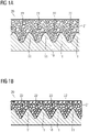
- Figure 1A shows a schematic sectional view of an electrical connection between a first contact 10 and a second contact 20 that has already been joined using the method according to the invention of the contact 10 are formed.
- the pins or rows of pins 11 are preferably arranged at regular intervals and particularly preferably in a square grid.
- the second contact 20 has an area 21 with a porous or foam-like, or more generally speaking, a soft, electrically conductive material compared to the pegs, into which the pegs 11 are already fully inserted.
- the material in the area 21 is partially displaced during the insertion of the pins, in particular in the partial areas 22 of the area 21 enclosing the pins 11, and in any case also partially compressed in the process.
- an at least slight, intentional deformation of the pins 11 during insertion into the area 21 take place.
- pins with a core made of a harder material can be covered with a soft(er) material in order to promote mutual deformation during the insertion process and to achieve better contact.
- the pins 11 are in the example Figure 1A essentially in the form of a circular cone, but can of course also assume other suitable shapes, for example cylindrical with a circular cross-section. However, other cross-sections such as ellipses, triangles, quadrilaterals, in particular squares, etc., can also be considered, which can also assume more complex shapes, which can therefore have tapers, undercuts or connections to one another (when viewed from the side). It is also possible to configure the pins in the form of a column or pillar, ie with a small diameter compared to the length, for example with a length of 2.0 mm and a diameter of 0.5 mm. In other configurations it is possible to choose tapered tenons, as in Figure 1A implied.
- the number, shape and dimensions of the pins can be freely selected within a wide range depending on the application and the manufacturing technology selected for the pins and the conductive material of the partner contact. It is thus possible, for example with only a low electrical or thermal load, to provide a few pins or just one pin. In other applications, however, it makes sense to use a large number of pegs, for example in order to increase the total contacting area, which increases with the number of pegs or pillars.
- the pegs can be made by various methods. For example, methods can be considered in which the respective contact 10 is produced with the pins 11 in one process step, ie for example embossing or die-casting methods, but also those described below Methods that are particularly suitable for producing studs or pillars directly on a semiconductor component.
- additive manufacturing processes are particularly useful there, but also galvanic manufacturing processes and thermal spraying processes and/or sintering processes, in particular with silver.
- thermal spraying process is used here as a generic term for the following processes, among others: application of material by atomization from a melt (melt pool spraying), application of material by electrical arc or gas discharge (e.g. arc spraying or plasma spraying), application of material by gas expansion without Combustion (e.g. cold gas spraying), application of material using combustion processes (e.g. wire flame spraying, powder flame spraying, high-velocity flame spraying, detonation spraying) or application of material using concentrated energetic beams (e.g. laser spraying).
- Cu, Ag, Au, Fe, Sn, Ni, Al, Mo, Wo or alloys of at least one of these elements come into consideration as material for the pins or pillars.
- semi-metals, metal-ceramics, highly doped semiconductors such as Si, SiC, GaN or graphite-based materials can also be used.
- the pegs or pillars can also be constructed from different material combinations, such as copper on one end of the pillar and graphite on the other end.
- the pegs can be plated with a metallic material or solder, for example Sn, Au, Ag.
- a metallic material or solder for example Sn, Au, Ag.
- Au oxide-free surface
- Sn soft metal
- the area 21 is in the in 1 example shown as uniform. In other embodiments, however, it is readily possible to divide the area provided for receiving the pins into sub-areas or connection islands which adjoin one another or can be separated by areas without soft material. It is also possible to equip these sub-areas with different soft material in order to ensure the contact quality over a wide temperature range, for example by choosing a soft material with good conductivity in a first, lower temperature range in a first sub-area and another in a second sub-area soft material is chosen with good conductivity in a second temperature range above the first temperature range.
- the contacts 10, 20 can be arranged on or on any circuit elements, connectors and the circuit carrier itself or formed integrally therewith (not shown).
- the circuit carrier can be a conventional Printed Circuit Board (PCB), an Active Metal Braze Substrate (AMB) or a Direct Copper Bond (DCB) carrier, one or more lead frames or an organic thick copper polymer substrate.
- Thick copper substrate means copper thicknesses of more than 0.3 mm, for example 1.0 mm, 2.0 mm or 4.0 mm.
- the circuit element can be an active or passive circuit element, in particular a power semiconductor.
- the circuit element can be applied to the carrier on the carrier side using the method described here or using a conventional method, for example by soldering or by sintering methods or by the method disclosed in the parallel patent application described in more detail above.
- a circuit element can have contacts of the type described here on one side or on several sides. In this case, the circuit element can only have contacts with pins or only contacts with soft areas as well as a combination of both types of contact.
- the contact that can be achieved after joining with only a low joining force is already sufficient, both for the electrical conductivity of the contact and for the thermal conductivity of the contact, as far as the thermal conductivity of the contact is concerned respective use case matters at all.
- the soft material 21 after joining it is advantageous to further compress the soft material 21 after joining.
- the result of the compression is in Figure 1B shown in a schematic sectional view.
- the compaction can be achieved by various measures. In particular, the following are possible: the exercise of a joint force with which the in Figure 1A condition shown is reached, exceeding compaction force; laser machining; heat treatment, preferably at temperatures lower than those encountered in soldering; delivery of energy by means of ultrasound; as well as suitable combinations of these measures, for example heating the joint before exerting a compression force.
- the entire area 21 and in particular the partial areas 22 enclosing the pegs 11 is compressed, as a result of which, for example, the electrical conductivity of the soft material and/or its temperature resistance can be improved.
- the pegs 11 and the contact 20 by suitably designing the pegs 11 and the contact 20 and in particular the area 21 equipped with material that is soft in relation to the peg material, it can be achieved that the pegs 11 are in direct mechanical and electrical contact with a harder base layer after compression of the soft material 21 (see also 2 ) of the contact 20 are, for example, to further increase the electrical conductivity and reliability of the contact.
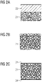
- the electrically conductive material 21 of the contact 20 which is soft compared to the pins and is applied to a flat carrier 23 which is harder in comparison, for example a metal sheet 23 .
- a gradual transition between the carrier and the porous material can be designed.
- the carrier and the soft material are delimited from one another largely without transitions.
- the connection with the pins takes place from below, ie on the side of the contact which has the soft material 21 .
- the contact 20 essentially consists of the porous or foam-like or soft, electrically conductive material 21 compared to the pin, ie the soft material 21 is selected so that it forms a mechanically stable contact 20 without a separate carrier, but is still soft compared to the pin material is enough to allow penetration of the studs (possibly using a tool that secures the shape of the contact 20) without deforming the contact 20 to the point of being unusable.
- the soft material 21 is selected so that it forms a mechanically stable contact 20 without a separate carrier, but is still soft compared to the pin material is enough to allow penetration of the studs (possibly using a tool that secures the shape of the contact 20) without deforming the contact 20 to the point of being unusable.
- it makes sense to compact the soft material 21 after it has been joined to the pins 11, as in connection with FIG Figure 1B already explained.
- Advantageous has the in Figure 2B
- the contact shown does not have a preferred mounting direction, so it can be joined to the pins from any
- a sandwich design for a contact 20 is shown, in which the porous or foam-like material 21 of the contact 20, which is soft relative to the pin, is embedded between two flat carriers 24, which consist of a material that is harder than the soft material and in which it can be sheet metal, for example.
- the thickness of the sheets 24 can be approximately the same, or a greater thickness and/or a harder material is selected for one of the sheets than for the other sheet. This more resistant sheet then forms the contact support, while the other sheet stabilizes and protects the soft material 21 .
- the assembly with the tenons is carried out on the side of the contact that has the less resistive sheet 24, the tenons being suitably shaped to pierce the less resistive sheet during the assembly operation, or with appropriate holes being made prior to assembly with the tenons be introduced into the less resistant sheet metal.
- the two sheets 24 are of approximately the same strength and are selected together with the soft material 21 in such a way that the combination of sandwich sheets 24 and soft material 21, which holds the sheets 24 together, ensures the desired mechanical properties of the contact 20.
- the joining with the pegs can take place from two directions, namely preferably perpendicular to the planes spanned by the metal sheets 24, in the representation of FIG Figure 2C i.e. from above and below.
- bent metal sheets at least partially cover the soft material enclose, and/or contacts in which several, preferably four, metal sheets enclose the soft material in the longitudinal direction (ie from left to right in the representation of the Figure 2C ) completely enclose, which then result in corresponding further contacting directions.
- "sandwich shape" is to be understood here as limited to two substantially parallel sheets 24 .
- the soft material 21 and, if necessary, the metal sheets 23, 24 are selected in such a way that the desired mechanical properties of the contact 20 are ensured.
- the contact 20 can be in the form of a contact tab protruding from the component, with corresponding requirements for flexibility combined with mechanical strength.
- the contact 20 can be arranged flat on a surface of the component and is mechanically stabilized by this surface or by the component itself.
- the soft material can be used as in Figure 2B shown without further layers or as in Figures 2A and 2C shown with limiting outer layers 23, 24 are used,
- a layer 23, 24 can act as a carrier material and can preferably consist of copper. It is used for mechanical stability and additional enlargement of the conductor cross-section.
- the side that is intended for joining with the pin(s) can be made thinner than a side that is not intended for joining.
- This joining side can in particular be made very thin in the manner of a skin and preferably consist of the same material as the soft material.
- asymmetrical sandwich designs are also possible, for example by applying a soft, porous or foam-like metal to a flat copper carrier, which has a flat outer skin, i.e. a thin layer, on the joining side, which is created during the manufacturing process, for example and is not subsequently removed or is applied in an additional manufacturing step.
- the exemplary embodiments of the present invention refer to power semiconductors, because reliable contacting that is as large as possible, as close as possible to the chip and therefore as possible without the supply of heat is of particular importance there.
- the invention is of course not limited to power semiconductors, but can be used in connection with all components that can be mounted on circuit carriers, either actively or passively.
Abstract
Die vorliegende Erfindung betrifft elektrische Kontakte und ein Verfahren zum Herstellen einer elektrischen Verbindung zwischen diesen Kontakten. Ein erster elektrischer Kontakt (10) weist einen flächigen Abschnitt auf, auf dem mindestens ein Zapfen (11) ausgebildet ist, der zum Einbringen in einen ein poröses oder schaumartiges leitfähiges Material aufweisenden Bereich (21) des zweiten Kontakts (20) ausgebildet ist. Die elektrische Verbindung entsteht durch Einbringen der Zapfen (11) in den weichen Bereich (21), wobei dabei eine zumindest teilweise Verdrängung des porösen oder schaumartigen leitfähigen Materials (21) durch den Zapfen (11) stattfindet.The present invention relates to electrical contacts and a method of making an electrical connection between these contacts. A first electrical contact (10) has a flat section on which at least one peg (11) is formed, which is formed for introduction into a porous or foam-like conductive material having area (21) of the second contact (20). The electrical connection is created by inserting the pegs (11) into the soft area (21), with the porous or foam-like conductive material (21) being at least partially displaced by the peg (11).
Description
Die vorliegende Erfindung betrifft eine neuartige Aufbau- und Verbindungstechnik, insbesondere für die Leistungselektronik.The present invention relates to a new construction and connection technology, in particular for power electronics.
Die Aufbau- und Verbindungstechnik hat die Aufgabe, elektrische und mechanische Verbindungen zwischen den einzelnen Elementen einer Schaltung und ggf. einem Schaltungsträger zu schaffen.The construction and connection technology has the task of creating electrical and mechanical connections between the individual elements of a circuit and, if necessary, a circuit carrier.
Insbesondere für Leistungshalbleiter hat es sich als vorteilhaft herausgestellt, diese mit Kontakten oder Kontaktflächen an mehreren Seiten auszustatten, also beispielsweise leiterplattenseitigen Kontakten und oberseitigen Kontakten. Verschiedene Aufbau- und Verbindungstechniken sind bekannt und in der Publikation "
Das dort beschriebene Drahtbonden an der Oberseite hat allerdings den Nachteil, dass während der Herstellung der Verbindung Kräfte aufgewendet werden, durch welche das Halbleiterbauelement beschädigt werden können. Zudem können im Betrieb lokale Temperaturerhöhungen entstehen, denen durch die Verwendung von mehreren Bonddrähten und dem sogenannten Stitching nur bedingt entgegengewirkt werden kann. Die Kontaktierungspunkte sind unvermeidbar einer punktuellen thermischen Belastung ausgesetzt und auch die Bonddrähte erwärmen sich aufgrund des während des Betriebs durch sie fließenden Stroms und ihres durch das Bondverfahren begrenzten Querschnitts. Ferner können aufgrund von Induktion in den Bonddrähten unerwünschte elektrische Störsignale in die Schaltung eingebracht werden, insbesondere kann bei parallel verlaufenden Bonddrähten, die zu verschiedenen Kontakten führen, ein unerwünschtes Übersprechen auftreten.However, the wire bonding described there on the upper side has the disadvantage that forces are applied during the production of the connection, as a result of which the semiconductor component can be damaged. In addition, local temperature increases can occur during operation, which can only be counteracted to a limited extent by using several bonding wires and so-called stitching. The contacting points are unavoidably exposed to localized thermal stress and the bonding wires also heat up due to the current flowing through them during operation and their cross section, which is limited by the bonding process. Furthermore, undesired electrical interference signals can be introduced into the circuit due to induction in the bonding wires undesired crosstalk can occur, particularly with parallel bonding wires that lead to different contacts.
Als Alternative zu Bonddrähten sind u.a. aus vorstehend genannter Publikation Sinterverfahren bekannt, die im Gegensatz zu den Bonddrähten flächige Verbindungen mit deutlich größeren Querschnitten erlauben und sowohl trägerseitig als auch oberseitig einsetzbar sind und sich gegenüber Lötverbindungen durch eine deutlich höhere Temperaturbeständigkeit auszeichnen. Nachteilig an diesen Sinterverfahren ist jedoch der hohe Fertigungsaufwand bei Bestückung der Leiterplatten bzw. Schaltungsträger und insbesondere der hohe Druck, der für den Sintervorgang erforderlich ist.As an alternative to bonding wires, sintering processes are known from the above-mentioned publication, which, in contrast to bonding wires, allow flat connections with significantly larger cross sections and can be used both on the carrier side and on the top side and are characterized by a significantly higher temperature resistance than soldered connections. A disadvantage of this sintering process, however, is the high production cost when assembling the printed circuit boards or circuit carriers and, in particular, the high pressure that is required for the sintering process.
Schließlich sind u.a. ebenfalls aus der vorstehend genannten Publikation Druckkontaktierungen bekannt, die an die Stelle der vorgenannten stoffschlüssigen Verbindungsarten treten. Dabei gleiten die verbundenen Partner aufeinander und vermeiden damit thermische Spannungen, die bei den stoffschlüssigen Verbindungen im Betrieb zwangsläufig auftreten und z.B. mittels geeignet flexibler Materialien kompensiert werden müssen. Druckkontaktierungen haben allerdings den Nachteil, dass auf den Halbleiter dauerhaft Druck ausgeübt wird, der sich mit der Temperatur ändert und das Halbleiterbauelement im Laufe der Zeit beschädigen kann. Zudem erfordern flächige Kontaktierungen perfekt ebene Flächen und es muss sichergestellt werden, dass die aufeinander gleitenden Kontakte dauerhaft frei von Verschmutzungen und Oxidschichten bleiben.Finally, pressure contacts are also known from the above-mentioned publication, among other things, which take the place of the aforementioned types of material-to-material connection. The connected partners slide on top of each other, thereby avoiding thermal stresses that inevitably occur with material connections during operation and must be compensated for, for example, using suitably flexible materials. However, pressure contacts have the disadvantage that pressure is constantly being exerted on the semiconductor, which pressure changes with temperature and can damage the semiconductor component over time. In addition, flat contacts require perfectly flat surfaces and it must be ensured that the contacts sliding on each other remain permanently free of dirt and oxide layers.
Aus der
Eine Aufgabe der vorliegenden Erfindung ist es, eine weiter verbesserte Aufbau- und Verbindungstechnik anzugeben.One object of the present invention is to specify a further improved construction and connection technique.
Diese Aufgabe wird durch besonders geformte elektrische Kontakte eines auf einen Schaltungsträger aufbringbaren Schaltungselements sowie des dazu passenden elektrischen Verbinders gelöst. Erfindungsgemäß weist einer der Kontakte einen flächigen Abschnitt auf, auf dem ein Zapfen ausgebildet ist, und der Partnerkontakt weist einen Bereich mit einem porösen oder schaumartigen leitfähigen Material auf, in welches der Zapfen eingebracht werden kann. Im gefügten Zustand bildet der Zapfen mit dem Bereich eine elektrisch leitende Verbindung.This object is achieved by specially shaped electrical contacts of a circuit element that can be applied to a circuit carrier and the electrical connector that matches it. According to the invention, one of the contacts has a flat section on which a peg is formed, and the partner contact has an area with a porous or foam-like conductive material into which the peg can be inserted. In the joined state, the pin forms an electrically conductive connection with the area.
Die vorliegende Erfindung betrifft ferner ein Verfahren zum Herstellen einer elektrisch leitenden Verbindung zwischen einem auf einem Schaltungsträger anbringbaren Schaltungselement und einem weiteren Element, die über Kontakte wie vorstehend beschrieben verfügen. Zur Herstellung der elektrisch leitenden Verbindung wird der Zapfens in den Bereich dem porösen oder schaumartigen leitfähigen Material eingebracht und dabei erfolgt eine teilweises Verdrängung des porösen oder schaumartigen leitfähigen Materials durch den Zapfen und somit wird eine elektrisch leitfähige Verbindung bewirkt.The present invention also relates to a method for producing an electrically conductive connection between a circuit element which can be fitted on a circuit carrier and a further element which have contacts as described above. To produce the electrically conductive connection, the peg is introduced into the region of the porous or foam-like conductive material, and the porous or foam-like conductive material is partially displaced by the peg, thus effecting an electrically conductive connection.
Die erfindungsgemäße Aufbau- und Verbindungstechnik hat dabei den wichtigen Vorteil, dass zuverlässige und dauerhafte elektrische und mechanische Verbindungen geschaffen werden können, und zwar in vielen Fällen ohne Erhitzen der Verbindungsstelle. Halbleiter können also bei Raumtemperatur angebunden werden und es können damit z.B. auch innerhalb polymerbasierter Gehäuse Verbindungen hergestellt werden, ohne dass (wie bei herkömmlichen wärmebasierten Fügeverfahren wie Löten oder Sintern) Sorge getragen werden muss, dass das Gehäuse durch die Erwärmung beschädigt wird. Nach Herstellen der Verbindung wird vorteilhafterweise kein Druck mehr auf die Schaltungselemente ausgeübt.The structure and connection technology according to the invention has the important advantage that reliable and permanent electrical and mechanical connections can be created, and in many cases without heating the connection point. Semiconductors can therefore be connected at room temperature and connections can also be made within polymer-based housings, for example, without having to worry (as with conventional heat-based joining methods such as soldering or sintering) that the Housing is damaged by heating. After the connection has been made, advantageously no more pressure is exerted on the circuit elements.
Dabei spielt es keine Rolle, welcher der Kontakte den Zapfen und welcher der Kontakte den Bereich mit einem porösen oder schaumartigen leitfähigen Material aufweist.It does not matter which of the contacts has the pin and which of the contacts has the area with a porous or foam-like conductive material.
In Ausführungsbeispielen wird die Kontaktierung durch mehrere Zapfen bewirkt, die in einen Bereich mit einem porösen oder schaumartigen leitfähigen Material des Partnerkontakts eingebracht werden. Dabei muss es sich nicht um einen einheitlichen Bereich handeln. Vielmehr kann der Partnerkontakt auch mehrere getrennte Bereiche mit porösem oder schaumartigem leitfähigen Material aufweisen, die die Mehrzahl der Zapfen aufnehmen. In besonderen Fällen kann dabei je Zapfen ein strukturell abgegrenzter, vorzugsweise zum Zapfen passend dimensionierter Bereich am Partnerkontakt vorgesehen sein. Im Falle mehrerer Zapfen kann zudem vorgesehen sein, dass diese im Wesentlichen zeitgleich mit dem/den das poröse oder schaumartige leitfähige Material aufweisenden Bereich/en gefügt werden.In exemplary embodiments, the contacting is effected by a plurality of pegs which are introduced into an area with a porous or foam-like conductive material of the partner contact. It doesn't have to be a unified area. Rather, the partner contact can also have several separate areas with porous or foam-like conductive material, which accommodate the majority of the pins. In special cases, a structurally delimited area, preferably dimensioned to match the pin, can be provided on the partner contact for each pin. In the case of several pegs, provision can also be made for these to be joined essentially at the same time as the area(s) having the porous or foam-like conductive material.
Die Zapfen können in einem Raster angeordnet sein, vorzugsweise in einem quadratischen Raster.The pins can be arranged in a grid, preferably in a square grid.
Das poröse das poröse oder schaumartige leitfähige Material kann nach Einbringen des Zapfens verdichtet werden, beispielsweise um die Leitfähigkeit und/oder die Stromtragefähigkeit der Verbindung zu erhöhen.The porous, porous or foam-like conductive material can be compacted after the pin has been introduced, for example in order to increase the conductivity and/or the current-carrying capacity of the connection.
Dabei kann die Verdichtung mittels Pressung und/oder Laserbearbeitung und/oder Wärmebehandlung und/oder mittels Ultraschall bewirkt werden.In this case, the compression can be effected by means of pressing and/or laser processing and/or heat treatment and/or by means of ultrasound.
Bei den Zapfen kann es sich dabei um Zapfen handeln, die nicht nur für die hier detailliert beschriebene Fügung mit einem porösen oder schaumartigen Material ausgebildet sind, sondern gleichzeitig ausgebildet sind, fallweise mit Partnerkontakten verbunden zu werden, welche zu den Zapfen passende Aussparungen aufweisen, wobei die Zapfen mit den Aussparungen kaltgeschweißte Verbindungen eingehen. Diese Aufbau- und Verbindungstechnik ist in der taggleich mit der vorliegenden Anmeldung eingereichten europäischen Patentanmeldung der gleichen Anmelderin im dem Titel "Auf einen Schaltungsträger aufbringbares Schaltungselement, elektrischer Verbinder sowie Verfahren zum Herstellen einer elektrischen Verbindung" detailliert beschrieben. Zudem ist es auch möglich, einen oder mehrere Zapfen mittels Kaltverschweißung oder Verpressung in Aussparungen des Partnerkontakts, insbesondere in solchen der in der genannten parallelen Anmeldung offenbarten Art, mit dem Partnerkontakt elektrisch leitend zu verbinden und einen oder mehrere Zapfen mittels Fügung mit einem Bereich mit einem porösen oder schaumartigen Material gemäß der vorliegenden Erfindung zu verbinden. Insbesondere kann/können dabei ein, zwei oder mehrere Fügepaare umfassend jeweils einen Zapfen und eine Aussparung beispielsweise zur Präzisionsausrichtung der Fügepartner zueinander verwendet werden und zudem als Teil der elektrischen Kontaktierung dienen, während andere Zapfen mit dem Bereich mit dem porösen oder schaumartigen Material kontaktiert und auf diese Weise unnötige mechanische Beanspruchungen oder sogar Fehlkontaktierungen zu vermieden werden, die beispielsweise aufgrund von Fertigungstoleranzen auftreten können, wenn eine Mehrzahl von Zapfen mit einer Mehrzahl von Aussparungen gefügt werden.The pegs can be pegs that are not only designed for the joining described in detail here with a porous or foam-like material, but at the same time are designed to be occasionally connected to partner contacts which have recesses matching the pegs, the pegs entering into cold-welded connections with the recesses. This assembly and connection technique is described in detail in the European patent application filed on the same day as the present application by the same applicant entitled "Circuit element that can be applied to a circuit carrier, electrical connector and method for producing an electrical connection". In addition, it is also possible to connect one or more pins to the partner contact in an electrically conductive manner by means of cold welding or pressing in recesses of the partner contact, in particular in those of the type disclosed in the parallel application mentioned, and to connect one or more pins by means of joining to an area with a to connect porous or foam-like material according to the present invention. In particular, one, two or more joining pairs, each comprising a peg and a recess, can be used, for example, for the precision alignment of the joining partners to one another and also serve as part of the electrical contacting, while other pegs make contact with the area with the porous or foam-like material and in this way, unnecessary mechanical stresses or even faulty contacts can be avoided, which can occur, for example, due to manufacturing tolerances when a plurality of pins are joined with a plurality of recesses.
Anders ausgedrückt ist es möglich, die hier beschriebene Erfindung einschließlich aller hier beschriebenen Ausführungsbeispiele mit der in der vorstehend näher bezeichneten parallelen Anmeldung beschriebenen Erfindung einschließlich aller dort beschriebenen Ausführungsbeispiele zu kombinieren. Zur Vermeidung von Wiederholungen wird die parallele Anmeldung in vollem Umfang hier durch Verweis mit einbezogen.In other words, it is possible to combine the invention described here, including all exemplary embodiments described here, with the invention described in the parallel application described in more detail above, including all exemplary embodiments described there. To avoid repetition, the parallel application is incorporated herein by reference in its entirety.
Im folgenden werden Ausführungsbeispiele der vorliegenden Erfindung anhand von Zeichnungen näher erläutert. Es sei darauf hingewiesen, dass sämtliche vorstehend und nachfolgend offenbarten Varianten, Ausgestaltungen und Ausführungsbeispiele uneingeschränkt miteinander kombinierbar sind, und zwar sowohl hinsichtlich der Kontakte des Schaltungselements, des elektrischen Verbinders, als auch des Verfahrens.In the following, exemplary embodiments of the present invention are explained in more detail with reference to drawings. be it It is pointed out that all the variants, configurations and exemplary embodiments disclosed above and below can be combined with one another without restriction, both with regard to the contacts of the circuit element, the electrical connector and the method.
Es zeigen:
-
Fig. 1A in schematischer Darstellung ein Kontaktierung zwischen Zapfen und einem Bereich mit einem porösen oder schaumartigen Material gemäß eines Ausführungsbeispiels der vorliegenden Erfindung; -
Fig. 1B die Kontaktierung ausFig. 1A nach Verdichtung des porösen oder schaumartigen Materials; und -
Fig. 2A-C drei verschiedene Ausführungsbeispiele für den Aufbau eines Bereichs mit einem porösen oder schaumartigen Material in stark schematisierter Darstellung.
-
Figure 1A in a schematic representation of a contact between pins and an area with a porous or foam-like material according to an embodiment of the present invention; -
Figure 1B the contactFigure 1A after compaction of the porous or foam-like material; and -
Figures 2A-C three different exemplary embodiments for the construction of an area with a porous or foam-like material in a highly schematic representation.
Der zweite Kontakt 20 weist einen Bereich 21 mit einem porösen oder schaumartigen, oder allgemeiner ausgedrückt, einem gegenüber den Zapfen weichen, elektrisch leitfähigen Material auf, in das die Zapfen 11 bereits vollständig eingeführt sind. Das Material im Bereich 21 wird während des Einführens der Zapfen teilweise verdrängt, insbesondere in den die Zapfen 11 umschließenden Teilbereichen 22 des Bereichs 21, und dabei auch jedenfalls teilweise verdichtet. Umgekehrt kann in Ausführungsbeispielen auch eine zumindest leichte, gewollte Verformung der Zapfen 11 während des Einführens in den Bereich 21 stattfinden. So können beispielsweise Zapfen mit einem Kern aus einem härteren Material mit einem weich(er)en Material umkleidet werden, um die wechselseitige Verformung während des Einführvorgangs zu befördern und eine bessere Kontaktierung zu erreichen.The
Die Zapfen 11 sind im Beispiel der
Anzahl, Form und Dimension der Zapfen kann je nach Anwendung und der für Zapfen und das leitfähige Material des Partnerkontakts gewählten Herstellungstechnologie in einem breiten Rahmen frei gewählt werden. So ist es möglich, beispielsweise bei nur geringer elektrischer oder thermischer Belastung, wenige Zapfen oder auch nur einen Zapfen vorzusehen. In anderen Anwendungen ist es hingegen sinnvoll, eine Vielzahl von Zapfen zu verwenden, beispielsweise um die gesamte Kontaktierungsfläche, die mit der Zahl der Zapfen bzw. Pillars steigt, zu erhöhen.The number, shape and dimensions of the pins can be freely selected within a wide range depending on the application and the manufacturing technology selected for the pins and the conductive material of the partner contact. It is thus possible, for example with only a low electrical or thermal load, to provide a few pins or just one pin. In other applications, however, it makes sense to use a large number of pegs, for example in order to increase the total contacting area, which increases with the number of pegs or pillars.
Die Zapfen können durch verschiedene Verfahren hergestellt werden. Beispielsweise kommen Verfahren in Betracht, bei denen in einem Verfahrensgang der jeweiligen Kontakt 10 mit den Zapfen 11 erzeugt wird, also beispielsweise Präge- oder Druckgussverfahren, aber auch die im folgenden beschriebenen Verfahren, die sich besonders zum Herstellen von Zapfen oder Pillars direkt auf einem Halbleiterbauelement eignen.The pegs can be made by various methods. For example, methods can be considered in which the
Insbesondere dort bieten sich additive Fertigungsverfahren an, aber auch galvanische Fertigungsverfahren sowie thermische Sprühverfahren und/oder Sinterverfahren, insbesondere mit Silber. Der Begriff "thermische Sprühverfahren" wird hier als Oberbegriff u.a. für folgende Verfahren verwendet: Aufbringen von Material durch Zerstäuben aus einer Schmelze (Schmelzbadspritzen), Aufbringen von Material durch elektrische Lichtbogen- oder Gasentladung (z.B. Lichtbogenspritzen oder Plasmaspritzen), Aufbringen von Material durch Gasexpansion ohne Verbrennung (z.B. Kaltgasspritzen), Aufbringen von Material mit Hilfe von Verbrennungsprozessen (z.B. Drahtflammspritzen, Pulverflammspritzen, Hochgeschwindigkeitsflammspritzen, Detonationsspritzen) oder Aufbringen von Material mit Hilfe gebündelter energetischer Strahlen (z.B. Laserspritzen) .Additive manufacturing processes are particularly useful there, but also galvanic manufacturing processes and thermal spraying processes and/or sintering processes, in particular with silver. The term "thermal spraying process" is used here as a generic term for the following processes, among others: application of material by atomization from a melt (melt pool spraying), application of material by electrical arc or gas discharge (e.g. arc spraying or plasma spraying), application of material by gas expansion without Combustion (e.g. cold gas spraying), application of material using combustion processes (e.g. wire flame spraying, powder flame spraying, high-velocity flame spraying, detonation spraying) or application of material using concentrated energetic beams (e.g. laser spraying).
Als Material für die Zapfen bzw. Pillars kommen insbesondere Cu, Ag, Au, Fe, Sn, Ni, Al, Mo, Wo bzw. Legierungen aus mindestens einem dieser Elemente in Betracht. Aber auch Halbmetalle, Metall-Keramiken, hochdotierte Halbleiter wie beispielsweise Si, SiC, GaN oder graphitbasierte Materialien können verwendet werden. Die Zapfen bzw. Pillars können auch aus verschiedenen Materialkombinationen aufgebaut sein, wie z.B. Kupfer an einem Ende des Pillars und Graphit am anderen Ende.In particular, Cu, Ag, Au, Fe, Sn, Ni, Al, Mo, Wo or alloys of at least one of these elements come into consideration as material for the pins or pillars. However, semi-metals, metal-ceramics, highly doped semiconductors such as Si, SiC, GaN or graphite-based materials can also be used. The pegs or pillars can also be constructed from different material combinations, such as copper on one end of the pillar and graphite on the other end.
Um einen effizienten elektrischen Kontakt zwischen Zapfen und weichem Material zu gewährleisten, können die Zapfen mit einem metallischen Material oder Lot überzogen sein, beispielsweise mit Sn, Au, Ag. Hierdurch kann beispielsweise durch eine oxidfreie Oberfläche (Au) und/oder durch ein "Verschmieren" eines weichen Metalls (Sn) auf dem Zapfen eine Verbindung hoher Qualität mit dem weichen Material 21 erleichtert werden.In order to ensure efficient electrical contact between the pegs and the soft material, the pegs can be plated with a metallic material or solder, for example Sn, Au, Ag. As a result, a high-quality connection to the
Der Bereich 21 ist im in
Die Kontakte 10, 20 können auf bzw. an beliebigen Schaltungselementen, Verbindern sowie dem Schaltungsträger selbst angeordnet bzw. integral damit ausgebildet sein (nicht dargestellt). Beim Schaltungsträger kann es sich um ein herkömmliches Printed Circuit Board (PCB) handeln, ein Active Metal Braze Substrat (AMB) oder um einen Direct Copper Bond (DCB) Träger, um einen oder mehrere Leadframes oder um ein organische Dick-Kupfer-Polymer-Substrat. Mit Dick-Kupfer-Substrat sind dabei Kupferdicken von mehr als 0,3 mm gemeint, also beispielsweise 1,0 mm, 2,0 mm oder 4,0 mm.The
Beim Schaltungselement kann es sich um ein aktives oder passives Schaltungselement handeln, insbesondere um einen Leistungshalbleiter. Das Schaltungselement kann trägerseitig mit dem hier beschriebenen Verfahren auf dem Träger aufgebracht sein oder mit einem herkömmlichen Verfahren, beispielsweise durch Auflöten oder durch Sinterverfahren oder durch das in der weiter oben genauer bezeichneten parallelen Patentanmeldung offenbarte Verfahren. Ein Schaltungselement kann dabei einseitig oder auf mehreren Seiten Kontakte der hier beschriebenen Art aufweisen. Dabei kann das Schaltungselement sowohl nur Kontakte mit Zapfen als auch nur Kontakte mit weichen Bereichen als auch eine Kombination beider Kontaktformen aufweisen.The circuit element can be an active or passive circuit element, in particular a power semiconductor. The circuit element can be applied to the carrier on the carrier side using the method described here or using a conventional method, for example by soldering or by sintering methods or by the method disclosed in the parallel patent application described in more detail above. A circuit element can have contacts of the type described here on one side or on several sides. In this case, the circuit element can only have contacts with pins or only contacts with soft areas as well as a combination of both types of contact.
Für bestimmte Anwendungen und bestimmte Materialkombinationen zwischen Zapfenmaterial und weichem Material ist die nach Fügen mit einer nur geringen Fügekraft erreichbare Kontaktierung bereits ausreichend, sowohl für die elektrische Leitfähigkeit der Kontaktierung als auch für die thermische Leitfähigkeit der Kontaktierung, soweit es auf die thermische Leitfähigkeit der Kontaktierung im jeweiligen Anwendungsfall überhaupt ankommt.For certain applications and certain material combinations between pin material and soft material, the contact that can be achieved after joining with only a low joining force is already sufficient, both for the electrical conductivity of the contact and for the thermal conductivity of the contact, as far as the thermal conductivity of the contact is concerned respective use case matters at all.
In anderen Ausführungsbeispielen ist es vorteilhaft, das weiche Material 21 nach dem Fügen weiter zu verdichten. Das Ergebnis der Verdichtung ist in
Im Ergebnis ist der gesamte Bereich 21 und insbesondere die die Zapfen 11 umschließenden Teilbereichen 22 verdichtet, wodurch beispielsweise die elektrische Leitfähigkeit des weichen Materials und/oder seine Temperaturbeständigkeit verbessert werden können.As a result, the
In besonderen Ausführungsbeispielen kann durch geeignete Gestaltung der Zapfen 11 und des Kontakts 20 und insbesondere des mit bezüglich des Zapfenmaterials weichem Material ausgestatteten Bereichs 21 erreicht werden, dass die Zapfen 11 nach Verdichtung des weichen Materials 21 in direktem mechanischen und elektrischen Kontakt mit einer härteren Basisschicht (siehe hierzu
In
Im Beispiel der
Im Beispiel der
Im Beispiel der
In anderen Ausgestaltungen der in
In allen drei in
Für das weiche Material eignen sich besonders duktile und gut leitfähige reine Metall wie Kupfer, Silber, Aluminium, Nickel oder Zinn. Je nach Ausführung kann das weiche Material wie in
Bei Bauteilen, bei denen die Kontakte viel Wärme ableiten und/oder hohe Ströme transportieren sollen, kann eine Schicht 23, 24 als Trägermaterial fungieren und bevorzugt aus Kupfer bestehen. Es dient der mechanischen Stabilität und zusätzlichen Vergrößerung des Leiterquerschnitts.In the case of components in which the contacts are intended to dissipate a great deal of heat and/or transport high currents, a
Bei der Gestaltung als Sandwich gemäß
Es sind mit anderen Worten auch asymmetrische Sandwich-Ausführungen möglich, beispielsweise indem auf einem flächigen Träger aus Kupfer ein weiches poröses oder schaumartiges Metall aufgebracht ist, das auf der Fügeseite eine flächige Außenhaut, d.h. eine dünne Schicht, aufweist, die beispielsweise während des Herstellungsprozesses entsteht und anschließend nicht entfernt wird oder die in einem zusätzlichen Herstellungsschritt aufgetragen wird.In other words, asymmetrical sandwich designs are also possible, for example by applying a soft, porous or foam-like metal to a flat copper carrier, which has a flat outer skin, i.e. a thin layer, on the joining side, which is created during the manufacturing process, for example and is not subsequently removed or is applied in an additional manufacturing step.
Es sei darauf hingewiesen, dass die Ausführungsbeispiele der vorliegenden Erfindung auf Leistungshalbleiter Bezug nehmen, weil dort die zuverlässige, möglichst großflächige, möglichst chipnahe und deswegen möglichst ohne Zuführung von Wärme durchgeführte Kontaktierung von besonderer Bedeutung ist. Die Erfindung ist aber natürlich nicht auf Leistungshalbleiter beschränkt, sondern im Zusammenhang mit allen auf Schaltungsträgern montierbaren Bauelementen, aktiv oder passiv, einsetzbar.It should be pointed out that the exemplary embodiments of the present invention refer to power semiconductors, because reliable contacting that is as large as possible, as close as possible to the chip and therefore as possible without the supply of heat is of particular importance there. However, the invention is of course not limited to power semiconductors, but can be used in connection with all components that can be mounted on circuit carriers, either actively or passively.
Claims (9)
Priority Applications (1)
| Application Number | Priority Date | Filing Date | Title |
|---|---|---|---|
| EP21169988.9A EP4080564A1 (en) | 2021-04-22 | 2021-04-22 | Electrical contact of a circuit element which can be attached to a circuit holder or an electrical connector and method for producing an electrically conductive connection |
Applications Claiming Priority (1)
| Application Number | Priority Date | Filing Date | Title |
|---|---|---|---|
| EP21169988.9A EP4080564A1 (en) | 2021-04-22 | 2021-04-22 | Electrical contact of a circuit element which can be attached to a circuit holder or an electrical connector and method for producing an electrically conductive connection |
Publications (1)
| Publication Number | Publication Date |
|---|---|
| EP4080564A1 true EP4080564A1 (en) | 2022-10-26 |
Family
ID=75674605
Family Applications (1)
| Application Number | Title | Priority Date | Filing Date |
|---|---|---|---|
| EP21169988.9A Withdrawn EP4080564A1 (en) | 2021-04-22 | 2021-04-22 | Electrical contact of a circuit element which can be attached to a circuit holder or an electrical connector and method for producing an electrically conductive connection |
Country Status (1)
| Country | Link |
|---|---|
| EP (1) | EP4080564A1 (en) |
Citations (4)
| Publication number | Priority date | Publication date | Assignee | Title |
|---|---|---|---|---|
| US20140126165A1 (en) * | 2012-11-06 | 2014-05-08 | Infineon Technologies Austria Ag | Packaged Nano-Structured Component and Method of Making a Packaged Nano-Structured Component |
| DE102013219433A1 (en) * | 2013-09-26 | 2015-03-26 | Siemens Aktiengesellschaft | Electronic power module with elastic contacts and stack construction with such a power module |
| US20200006243A1 (en) * | 2017-03-24 | 2020-01-02 | Mitsubishi Electric Corporation | Semiconductor device and method of manufacturing same |
| WO2021013401A1 (en) | 2019-07-25 | 2021-01-28 | Siemens Aktiengesellschaft | Method and cooling body arrangement for cooling semidconductor chips having integrated electronic circuits for power electronic applications |
-
2021
- 2021-04-22 EP EP21169988.9A patent/EP4080564A1/en not_active Withdrawn
Patent Citations (4)
| Publication number | Priority date | Publication date | Assignee | Title |
|---|---|---|---|---|
| US20140126165A1 (en) * | 2012-11-06 | 2014-05-08 | Infineon Technologies Austria Ag | Packaged Nano-Structured Component and Method of Making a Packaged Nano-Structured Component |
| DE102013219433A1 (en) * | 2013-09-26 | 2015-03-26 | Siemens Aktiengesellschaft | Electronic power module with elastic contacts and stack construction with such a power module |
| US20200006243A1 (en) * | 2017-03-24 | 2020-01-02 | Mitsubishi Electric Corporation | Semiconductor device and method of manufacturing same |
| WO2021013401A1 (en) | 2019-07-25 | 2021-01-28 | Siemens Aktiengesellschaft | Method and cooling body arrangement for cooling semidconductor chips having integrated electronic circuits for power electronic applications |
Non-Patent Citations (1)
| Title |
|---|
| "Applikationshandbuch Leistungshalbleiter", 2015, HERAUSGEBER SEMIKRON INTERNATIONAL GMBH |
Similar Documents
| Publication | Publication Date | Title |
|---|---|---|
| EP3262666B1 (en) | Electrical element and method for manufacturing it | |
| DE102008005547B4 (en) | Power semiconductor module and circuit arrangement with a power semiconductor module | |
| DE2813968C2 (en) | Semiconductor device | |
| CH652533A5 (en) | SEMICONDUCTOR BLOCK. | |
| DE19830820A1 (en) | Electronic ceramic component and method for producing the electronic ceramic component | |
| EP2516321B1 (en) | Sensor comprising a preferably multilayered ceramic substrate and method for producing it | |
| EP1208573B1 (en) | Anode for electrolytic capacitors, electrolytic capacitor and method of producing said anode | |
| WO2003094252A2 (en) | Piezoactuator and method for the production thereof | |
| DE19809138A1 (en) | Printed circuit board with SMD components | |
| DE102013100701B4 (en) | SEMICONDUCTOR MODULE ARRANGEMENT AND METHOD FOR MANUFACTURING A SEMICONDUCTOR MODULE ARRANGEMENT | |
| DE102013211405A1 (en) | METHOD FOR PRODUCING A SEMICONDUCTOR MODULE | |
| EP1741162A2 (en) | Electric functional unit and method for the production thereof | |
| DE102014105000B4 (en) | Method for manufacturing and equipping a circuit carrier | |
| DE19924341A1 (en) | Electronic ceramic component and an attachment structure for the same | |
| WO2012076166A1 (en) | Printed circuit board | |
| EP3229566A1 (en) | Connection element for an electronic component arrangement and process to produce the same, electronic component arrangement and process to produce the same | |
| WO2006013145A1 (en) | Printed circuit board with smd components and at least one wired component and a method for picking fixing and electrical contacting of said components | |
| DE4015463A1 (en) | METHOD FOR ATTACHING CONDUCTIVE CONNECTIONS TO CERAMIC COMPONENTS | |
| DE19523977A1 (en) | Microchip fuse | |
| DE10103084B4 (en) | Semiconductor module and method for its production | |
| EP4080564A1 (en) | Electrical contact of a circuit element which can be attached to a circuit holder or an electrical connector and method for producing an electrically conductive connection | |
| EP4080563A1 (en) | Circuit element which can be attached to a circuit carrier, electrical connector and method for producing an electrical connection | |
| DE102009044933B4 (en) | Power semiconductor module with at least two connected circuit carriers and method for producing a power semiconductor module with at least two connected circuit carriers | |
| EP1714328A2 (en) | Piezo actuator and a method for the production thereof | |
| EP3740050A1 (en) | Printed circuit board with a connector |
Legal Events
| Date | Code | Title | Description |
|---|---|---|---|
| PUAI | Public reference made under article 153(3) epc to a published international application that has entered the european phase |
Free format text: ORIGINAL CODE: 0009012 |
|
| STAA | Information on the status of an ep patent application or granted ep patent |
Free format text: STATUS: THE APPLICATION HAS BEEN PUBLISHED |
|
| AK | Designated contracting states |
Kind code of ref document: A1 Designated state(s): AL AT BE BG CH CY CZ DE DK EE ES FI FR GB GR HR HU IE IS IT LI LT LU LV MC MK MT NL NO PL PT RO RS SE SI SK SM TR |
|
| STAA | Information on the status of an ep patent application or granted ep patent |
Free format text: STATUS: THE APPLICATION IS DEEMED TO BE WITHDRAWN |
|
| 18D | Application deemed to be withdrawn |
Effective date: 20230427 |