EP4080530A1 - Film capacitor element and film capacitor - Google Patents
Film capacitor element and film capacitor Download PDFInfo
- Publication number
- EP4080530A1 EP4080530A1 EP20903793.6A EP20903793A EP4080530A1 EP 4080530 A1 EP4080530 A1 EP 4080530A1 EP 20903793 A EP20903793 A EP 20903793A EP 4080530 A1 EP4080530 A1 EP 4080530A1
- Authority
- EP
- European Patent Office
- Prior art keywords
- film
- electrode
- films
- dielectric
- film capacitor
- Prior art date
- Legal status (The legal status is an assumption and is not a legal conclusion. Google has not performed a legal analysis and makes no representation as to the accuracy of the status listed.)
- Withdrawn
Links
Images


Classifications
-
- H—ELECTRICITY
- H01—ELECTRIC ELEMENTS
- H01G—CAPACITORS; CAPACITORS, RECTIFIERS, DETECTORS, SWITCHING DEVICES, LIGHT-SENSITIVE OR TEMPERATURE-SENSITIVE DEVICES OF THE ELECTROLYTIC TYPE
- H01G4/00—Fixed capacitors; Processes of their manufacture
- H01G4/30—Stacked capacitors
-
- H—ELECTRICITY
- H01—ELECTRIC ELEMENTS
- H01G—CAPACITORS; CAPACITORS, RECTIFIERS, DETECTORS, SWITCHING DEVICES, LIGHT-SENSITIVE OR TEMPERATURE-SENSITIVE DEVICES OF THE ELECTROLYTIC TYPE
- H01G4/00—Fixed capacitors; Processes of their manufacture
- H01G4/32—Wound capacitors
-
- H—ELECTRICITY
- H01—ELECTRIC ELEMENTS
- H01G—CAPACITORS; CAPACITORS, RECTIFIERS, DETECTORS, SWITCHING DEVICES, LIGHT-SENSITIVE OR TEMPERATURE-SENSITIVE DEVICES OF THE ELECTROLYTIC TYPE
- H01G4/00—Fixed capacitors; Processes of their manufacture
- H01G4/002—Details
- H01G4/005—Electrodes
- H01G4/012—Form of non-self-supporting electrodes
-
- H—ELECTRICITY
- H01—ELECTRIC ELEMENTS
- H01G—CAPACITORS; CAPACITORS, RECTIFIERS, DETECTORS, SWITCHING DEVICES, LIGHT-SENSITIVE OR TEMPERATURE-SENSITIVE DEVICES OF THE ELECTROLYTIC TYPE
- H01G4/00—Fixed capacitors; Processes of their manufacture
- H01G4/002—Details
- H01G4/018—Dielectrics
- H01G4/06—Solid dielectrics
- H01G4/14—Organic dielectrics
- H01G4/18—Organic dielectrics of synthetic material, e.g. derivatives of cellulose
-
- H—ELECTRICITY
- H01—ELECTRIC ELEMENTS
- H01G—CAPACITORS; CAPACITORS, RECTIFIERS, DETECTORS, SWITCHING DEVICES, LIGHT-SENSITIVE OR TEMPERATURE-SENSITIVE DEVICES OF THE ELECTROLYTIC TYPE
- H01G4/00—Fixed capacitors; Processes of their manufacture
- H01G4/002—Details
- H01G4/224—Housing; Encapsulation
-
- H—ELECTRICITY
- H01—ELECTRIC ELEMENTS
- H01G—CAPACITORS; CAPACITORS, RECTIFIERS, DETECTORS, SWITCHING DEVICES, LIGHT-SENSITIVE OR TEMPERATURE-SENSITIVE DEVICES OF THE ELECTROLYTIC TYPE
- H01G4/00—Fixed capacitors; Processes of their manufacture
- H01G4/002—Details
- H01G4/018—Dielectrics
- H01G4/02—Gas or vapour dielectrics
Definitions
- the present disclosure relates to a film capacitor element and a film capacitor including the film capacitor element.
- Patent Literature 1 A known technique is described in, for example, Patent Literature 1.
- Patent Literature 1 Japanese Unexamined Patent Application Publication No. 2015-211071
- a film capacitor element includes a body including a plurality of dielectric films, a plurality of first electrode films, and a plurality of second electrode films being stacked on one another or being wound together, a first external electrode at one end of the body and electrically connected to the plurality of first electrode films, and a second external electrode at another end of the body and electrically connected to the plurality of second electrode films.
- the body includes a capacitance portion in which each of the plurality of first electrode films faces a corresponding second electrode film of the plurality of second electrode films with a corresponding dielectric film of the plurality of dielectric films in between, and the capacitance portion includes spaces each between a corresponding dielectric film of the plurality of dielectric films and a corresponding first electrode film of the plurality of first electrode films or between a corresponding dielectric film of the plurality of dielectric films and a corresponding second electrode film of the plurality of second electrode films.
- a film capacitor according to one aspect of the present disclosure includes the film capacitor element, a housing accommodating the film capacitor element, and a sealant sealing the film capacitor element accommodated in the housing.
- a film capacitor element and a film capacitor including a wound body with at least a pair of dielectric films each including an electrode film on the surface wound together, and a pair of metal-sprayed electrodes on both ends of the wound body are described.
- the wound body includes an active portion in which electrode films in the pair of dielectric films overlap each other, and the diameter of the active portion is greater than the diameter of each metal-sprayed electrode in the cross section perpendicular to the winding axis of the wound body to reduce the volume ratio of each metal-sprayed electrode.
- the resultant film capacitor can have a smaller size and larger capacity.
- FIG. 1 is a schematic cross-sectional view of a film capacitor element according to one embodiment of the present disclosure, taken along one plane in a first direction X.
- a film capacitor element 1 includes a body 20 including multiple dielectric films 2a and 2b and film electrodes 6 including electrode films 4a and 4b on the surfaces of the dielectric films 2a and 2b stacked on one another or wound together.
- the film capacitor element 1 also includes a pair of external electrodes 3a and 3b on both ends of the body 20 in the first direction X connected to the electrode films 4a and 4b in the multiple film electrodes 6 to form a capacitance portion 20c (active portion).
- the capacitance portion 20c is at the middle between the ends of the body 20 in the first direction X.
- the body 20 has spaces S between the film electrodes 6.
- the dielectric films 2a and 2b are plastically deformed with the spaces S in the stacking direction.
- the width of each space S or specifically, the distance in the stacking direction between adjacent film electrodes 6 across the space S, is, for example, at least 0.5 ⁇ m.
- the width of each space S may be, for example, one or more times the thickness of the dielectric film 2a or 2b, or two or more times the thickness of the dielectric film 2a or 2b.
- Each film electrode 6 has multiple microscopic recesses 7 on its surface.
- Each recess 7 may be replaced by a hole that is circular, oval, polygonal, or star-shaped in a plan view, or a groove that is linear, arc-shaped, or dendritic in a plan view.
- Each recess 7 may also be replaced by two or more holes or grooves connected together.
- the depth of each recess 7 may be, for example, 10 nm or greater and less than or equal to half the thickness of the dielectric film 2a or 2b.
- the diameter of the recess 7 in a plan view may be, for example, from 10 nm to 2 ⁇ m inclusive.
- the width of the recess 7 in a plan view may be, for example, from 10 nm to 2 ⁇ m inclusive, and the length may be, for example, 200 ⁇ m or less.
- the density of the recesses 7 may be, for example, 1 to 1000 recesses/mm 2 or less.
- the recesses 7 have the ratio of the diameter to the depth of the hole (diameter/depth) or the ratio of the width to the depth of the groove (width/depth) being 3 or less.
- the dielectric film 2a or 2b may be simply referred to as the dielectric film 2.
- the electrode film 4a or 4b may be simply referred to as the electrode film 4.
- the film capacitor element 1 may be fabricated with the procedure described below.
- the dielectric film 2 is prepared first.
- the dielectric film 2 is obtained by, for example, preparing a resin solution by dissolving an insulating resin in a solvent, applying the resin solution on the surface of a base film of, for example, polyethylene terephthalate (PET) in a sheet, and drying the sheet to volatilize the solvent.
- PET polyethylene terephthalate
- the sheet may be applied with a method selected as appropriate from known film deposition methods including doctor blading, die coating, and knife coating.
- Examples of the solvent used for the sheet include methanol, isopropanol, n-butanol, ethylene glycol, ethylene glycol monopropyl ether, methyl ethyl ketone, methyl isobutyl ketone, xylene, propylene glycol monomethyl ether, propylene glycol monomethyl ether acetate, dimethylacetamide, cyclohexane, and an organic solvent containing a mixture of two or more solvents selected from the above solvents.
- the dielectric film 2 can also be formed by stretching a film of resin formed by melt extrusion.
- the dielectric film 2 may have the thickness of, for example, 5 ⁇ m or less, or specifically the thickness of 0.5 to 2 ⁇ m.
- the insulating resin for the dielectric film 2 examples include polypropylene (PP), PET, polyphenylene sulfide (PPS), polyethylene naphthalate (PEN), polyarylate (PAR), polyphenylene ether (PPE), polyetherimide (PEI), and cycloolefin polymers (COPs).
- the insulating resin may specifically be COPs having a high insulation breakdown voltage.
- the dielectric film 2 may contain the insulating resin selected from the above examples alone or may include other materials.
- the materials that may be included in the dielectric film 2 other than the resin include, for example, the above organic solvent and an inorganic filler.
- the inorganic filler include an inorganic oxide such as alumina, titanium oxide, or silicon dioxide, an inorganic nitride such as silicon nitride, and glass.
- a material with a high relative dielectric constant such as a composite oxide having a perovskite structure may be used as an inorganic filler.
- the dielectric film 2 has a higher relative dielectric constant across the film.
- the film capacitor using this dielectric film 2 can have a smaller size.
- the inorganic filler may be surface-treated by, for example, silane coupling treatment or titanate coupling treatment.
- FIG. 2A is a diagram describing a procedure for expanding air and other gases remaining in the film electrodes 6.
- the electrode films 4 are eliminated for ease of illustration.
- the film capacitor element 1 including the film electrodes 6 with the multiple microscopic recesses 7 being stacked may be, for example, heated to expand air remaining in the microscopic recesses 7.
- the expanded air enters between the film electrodes 6, forming the spaces S between the film electrodes 6.
- the dielectric film 2 is plastically deformed with the spaces S being formed. When the film capacitor element 1 is cooled, the spaces S remain between the film electrodes 6.
- the film capacitor element 1 including the film electrodes 6 with the multiple microscopic recesses 7 being stacked may be accommodated in a container, and the container accommodating the film capacitor element 1 may be evacuated to expand the air in the microscopic recesses 7 on the film electrode 6.
- the expanded air enters between the film electrodes 6, forming the spaces S between the film electrodes 6.
- the dielectric film 2 is plastically deformed with the spaces S being formed.
- the container accommodating the film capacitor element 1 is under the atmospheric pressure, the spaces S remain between the film electrodes 6.
- the film capacitor element 1 including the film electrodes 6 with the multiple microscopic recesses 7 being stacked may be accommodated in a container.
- the container accommodating the film capacitor element 1 may be evacuated, and the film capacitor element 1 may be heated to expand the air in the recesses 7 on the film electrode 6 more easily.
- FIG. 2B is a diagram describing a procedure for vaporizing a solvent remaining in the film electrodes 6.
- the electrode films 4 are eliminated for ease of illustration.
- the film capacitor element 1 including the film electrodes 6 being stacked may be, for example, heated to vaporize the solvent remaining between the film electrodes 6.
- the vaporized solvent enters between the film electrodes 6 to form the spaces S between the film electrodes 6.
- the dielectric film 2 is plastically deformed with the spaces S being formed. When the film capacitor element 1 is cooled, the spaces S remain between the film electrodes 6.
- FIG. 3 is a diagram of the film capacitor element 1 encapsulated with a resin.
- L max - 1 m is the maximum thickness difference
- (L max - l m )/l m ⁇ 100 is the maximum expansion rate (%) in the stacking direction, where L max is the dimension of the expanded body 20 in the stacking direction, and l m is the dimension of the external electrode 3a or 3b in the stacking direction.
- the maximum thickness difference and the maximum expansion rate in the stacking direction are both greater than 0.
- the maximum thickness difference may be, for example, greater than or equal to the thickness of the dielectric film 2 or greater than or equal to 0.5 ⁇ m.
- the maximum expansion rate in the stacking direction may be 100% or less, 50% or less, or specifically 25% or less.
- Terminals 5 are connected to the external electrodes 3a and 3b.
- FIG. 4 is a schematic diagram describing the pressure from the resin encapsulation applied to the film capacitor element 1.
- the dielectric film 2 in each layer is plastically deformed with the capacitance portion 20c between the pair of external electrodes 3a and 3b expanding in the stacking direction and the spaces S between the film electrodes 6 in the layers.
- the pressure applied to the capacitance portion 20c in the stacking direction is reduced with air or other gases in the spaces S between the film electrodes 6 in the layers.
- the gases in the spaces S may flow from gaps around the external electrodes 3a and 3b into the spaces S in the other layers. This further reduces the pressure applied to the capacitance portion 20c.
- This structure reduces the likelihood of high pressure being applied to the capacitance portion 20c in the stacking direction and reduces thermal damage to the film electrodes 6 due to contact between the film electrodes 6 under high pressure and thus reduces breaks from any short circuit.
- the spaces S may be formed at least partially in the stacking direction of the body 20.
- the spaces S may extend over both ends of the body 20 in the first direction X, or may extend partially between the two ends.
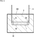
- FIG. 5 is a schematic cross-sectional view of a film capacitor according to one embodiment.
- a film capacitor 100 includes the film capacitor element 1 according to the above embodiment, a housing 10 accommodating the film capacitor element 1, and a sealant 9 sealing the film capacitor element 1 accommodated in the housing 10.
- the sealant 9 is, for example, a resin.
- the film capacitor 100 can be less susceptible to breaks due to a short circuit and is highly reliable.
- the film capacitor element is not limited to the film capacitor element 1 described in FIGs. 1 to 4 , but may be any other film capacitor element.
- the electrode films 4a and 4b and the dielectric films 2a and 2b without being joined together may be stacked on one another or wound together, without the electrode films 4a and 4b being formed on the dielectric films 2a and 2b.
- the film electrode 6 including the dielectric film 2a with an electrode film 4a on one surface of the dielectric film 2a and an electrode film 4b on the other surface of the dielectric film 2a, and the dielectric film 2b with no electrode films 4a and 4b may be stacked on one another or wound together.
- a film capacitor element includes a body including a plurality of dielectric films, a plurality of first electrode films, and a plurality of second electrode films being stacked on one another or being wound together, a first external electrode at one end of the body and electrically connected to the plurality of first electrode films, and a second external electrode at another end of the body and electrically connected to the plurality of second electrode films.
- the body includes a capacitance portion in which each of the plurality of first electrode films faces a corresponding second electrode film of the plurality of second electrode films with a corresponding dielectric film of the plurality of dielectric films in between, and the capacitance portion includes spaces each between a corresponding dielectric film of the plurality of dielectric films and a corresponding first electrode film of the plurality of first electrode films or between a corresponding dielectric film of the plurality of dielectric films and a corresponding second electrode film of the plurality of second electrode films.
- a film capacitor according to one aspect of the present disclosure includes the film capacitor element, a housing accommodating the film capacitor element, and a sealant sealing the film capacitor element accommodated in the housing.
- the film capacitor element and the film capacitor according to the embodiments of the present disclosure can reduce breaks due to a short circuit and are highly reliable.
Landscapes
- Engineering & Computer Science (AREA)
- Power Engineering (AREA)
- Manufacturing & Machinery (AREA)
- Microelectronics & Electronic Packaging (AREA)
- Fixed Capacitors And Capacitor Manufacturing Machines (AREA)
Abstract
Description
- The present disclosure relates to a film capacitor element and a film capacitor including the film capacitor element.
- A known technique is described in, for example,
Patent Literature 1. - Patent Literature 1:
Japanese Unexamined Patent Application Publication No. 2015-211071 - A film capacitor element according to one aspect of the present disclosure includes a body including a plurality of dielectric films, a plurality of first electrode films, and a plurality of second electrode films being stacked on one another or being wound together, a first external electrode at one end of the body and electrically connected to the plurality of first electrode films, and a second external electrode at another end of the body and electrically connected to the plurality of second electrode films. The body includes a capacitance portion in which each of the plurality of first electrode films faces a corresponding second electrode film of the plurality of second electrode films with a corresponding dielectric film of the plurality of dielectric films in between, and the capacitance portion includes spaces each between a corresponding dielectric film of the plurality of dielectric films and a corresponding first electrode film of the plurality of first electrode films or between a corresponding dielectric film of the plurality of dielectric films and a corresponding second electrode film of the plurality of second electrode films.
- A film capacitor according to one aspect of the present disclosure includes the film capacitor element, a housing accommodating the film capacitor element, and a sealant sealing the film capacitor element accommodated in the housing.
- The objects, features, and advantages of the present disclosure will be more apparent from the detailed description and the drawings below.
-
FIG. 1 is a schematic cross-sectional view of a film capacitor element according to one embodiment of the present disclosure, taken along one plane in a first direction X. -
FIG. 2A is a diagram describing a procedure for expanding air and other gases remaining in film electrodes. -
FIG. 2B is a diagram describing a procedure for vaporizing and expanding a solvent remaining in the film electrodes. -
FIG. 3 is a diagram of the film capacitor element encapsulated with a resin. -
FIG. 4 is a schematic diagram describing the pressure from the resin encapsulation applied to the film capacitor element. -
FIG. 5 is a schematic cross-sectional view of a film capacitor according to one embodiment of the present disclosure. - As the structure that forms the basis of the present disclosure, a film capacitor element and a film capacitor including a wound body with at least a pair of dielectric films each including an electrode film on the surface wound together, and a pair of metal-sprayed electrodes on both ends of the wound body are described. In this structure, the wound body includes an active portion in which electrode films in the pair of dielectric films overlap each other, and the diameter of the active portion is greater than the diameter of each metal-sprayed electrode in the cross section perpendicular to the winding axis of the wound body to reduce the volume ratio of each metal-sprayed electrode. The resultant film capacitor can have a smaller size and larger capacity.
- One or more embodiments of the film capacitor element will now be described.
- One or more embodiments of the present disclosure will now be described with reference to the drawings. The embodiments described below are mere examples of the present disclosure, and may be modified in various manners without departing from the spirit and scope of the present disclosure.
-
FIG. 1 is a schematic cross-sectional view of a film capacitor element according to one embodiment of the present disclosure, taken along one plane in a first direction X. Afilm capacitor element 1 includes abody 20 including multipledielectric films film electrodes 6 includingelectrode films dielectric films film capacitor element 1 also includes a pair ofexternal electrodes body 20 in the first direction X connected to theelectrode films multiple film electrodes 6 to form acapacitance portion 20c (active portion). Thecapacitance portion 20c is at the middle between the ends of thebody 20 in the first direction X. Thebody 20 has spaces S between thefilm electrodes 6. In other words, thedielectric films adjacent film electrodes 6 across the space S, is, for example, at least 0.5 µm. The width of each space S may be, for example, one or more times the thickness of thedielectric film dielectric film film electrode 6 has multiplemicroscopic recesses 7 on its surface. - Each
recess 7 may be replaced by a hole that is circular, oval, polygonal, or star-shaped in a plan view, or a groove that is linear, arc-shaped, or dendritic in a plan view. Eachrecess 7 may also be replaced by two or more holes or grooves connected together. The depth of eachrecess 7 may be, for example, 10 nm or greater and less than or equal to half the thickness of thedielectric film recess 7 being replaced by a hole, the diameter of therecess 7 in a plan view may be, for example, from 10 nm to 2 µm inclusive. For eachrecess 7 being replaced by a groove, the width of therecess 7 in a plan view may be, for example, from 10 nm to 2 µm inclusive, and the length may be, for example, 200 µm or less. The density of therecesses 7 may be, for example, 1 to 1000 recesses/mm2 or less. - The
recesses 7 have the ratio of the diameter to the depth of the hole (diameter/depth) or the ratio of the width to the depth of the groove (width/depth) being 3 or less. - The
dielectric film electrode film - The
film capacitor element 1 may be fabricated with the procedure described below. The dielectric film 2 is prepared first. The dielectric film 2 is obtained by, for example, preparing a resin solution by dissolving an insulating resin in a solvent, applying the resin solution on the surface of a base film of, for example, polyethylene terephthalate (PET) in a sheet, and drying the sheet to volatilize the solvent. The sheet may be applied with a method selected as appropriate from known film deposition methods including doctor blading, die coating, and knife coating. Examples of the solvent used for the sheet include methanol, isopropanol, n-butanol, ethylene glycol, ethylene glycol monopropyl ether, methyl ethyl ketone, methyl isobutyl ketone, xylene, propylene glycol monomethyl ether, propylene glycol monomethyl ether acetate, dimethylacetamide, cyclohexane, and an organic solvent containing a mixture of two or more solvents selected from the above solvents. The dielectric film 2 can also be formed by stretching a film of resin formed by melt extrusion. - The dielectric film 2 may have the thickness of, for example, 5 µm or less, or specifically the thickness of 0.5 to 2 µm.
- Examples of the insulating resin for the dielectric film 2 include polypropylene (PP), PET, polyphenylene sulfide (PPS), polyethylene naphthalate (PEN), polyarylate (PAR), polyphenylene ether (PPE), polyetherimide (PEI), and cycloolefin polymers (COPs). The insulating resin may specifically be COPs having a high insulation breakdown voltage.
- The dielectric film 2 may contain the insulating resin selected from the above examples alone or may include other materials. The materials that may be included in the dielectric film 2 other than the resin include, for example, the above organic solvent and an inorganic filler. Examples of the inorganic filler include an inorganic oxide such as alumina, titanium oxide, or silicon dioxide, an inorganic nitride such as silicon nitride, and glass. In particular, a material with a high relative dielectric constant such as a composite oxide having a perovskite structure may be used as an inorganic filler. In this case, the dielectric film 2 has a higher relative dielectric constant across the film. The film capacitor using this dielectric film 2 can have a smaller size. The inorganic filler may be surface-treated by, for example, silane coupling treatment or titanate coupling treatment.
-
FIG. 2A is a diagram describing a procedure for expanding air and other gases remaining in thefilm electrodes 6. InFIG. 2A , the electrode films 4 are eliminated for ease of illustration. Thefilm capacitor element 1 including thefilm electrodes 6 with the multiplemicroscopic recesses 7 being stacked may be, for example, heated to expand air remaining in themicroscopic recesses 7. The expanded air enters between thefilm electrodes 6, forming the spaces S between thefilm electrodes 6. The dielectric film 2 is plastically deformed with the spaces S being formed. When thefilm capacitor element 1 is cooled, the spaces S remain between thefilm electrodes 6. - In some embodiments, the
film capacitor element 1 including thefilm electrodes 6 with the multiplemicroscopic recesses 7 being stacked may be accommodated in a container, and the container accommodating thefilm capacitor element 1 may be evacuated to expand the air in themicroscopic recesses 7 on thefilm electrode 6. The expanded air enters between thefilm electrodes 6, forming the spaces S between thefilm electrodes 6. The dielectric film 2 is plastically deformed with the spaces S being formed. When the container accommodating thefilm capacitor element 1 is under the atmospheric pressure, the spaces S remain between thefilm electrodes 6. - In some embodiments, the
film capacitor element 1 including thefilm electrodes 6 with the multiplemicroscopic recesses 7 being stacked may be accommodated in a container. The container accommodating thefilm capacitor element 1 may be evacuated, and thefilm capacitor element 1 may be heated to expand the air in therecesses 7 on thefilm electrode 6 more easily. -
FIG. 2B is a diagram describing a procedure for vaporizing a solvent remaining in thefilm electrodes 6. InFIG. 2B , the electrode films 4 are eliminated for ease of illustration. Thefilm capacitor element 1 including thefilm electrodes 6 being stacked may be, for example, heated to vaporize the solvent remaining between thefilm electrodes 6. The vaporized solvent enters between thefilm electrodes 6 to form the spaces S between thefilm electrodes 6. The dielectric film 2 is plastically deformed with the spaces S being formed. When thefilm capacitor element 1 is cooled, the spaces S remain between thefilm electrodes 6. -
FIG. 3 is a diagram of thefilm capacitor element 1 encapsulated with a resin. Lmax - 1m is the maximum thickness difference, and (Lmax - lm)/lm × 100 is the maximum expansion rate (%) in the stacking direction, where Lmax is the dimension of the expandedbody 20 in the stacking direction, and lm is the dimension of theexternal electrode Terminals 5 are connected to theexternal electrodes -
FIG. 4 is a schematic diagram describing the pressure from the resin encapsulation applied to thefilm capacitor element 1. The dielectric film 2 in each layer is plastically deformed with thecapacitance portion 20c between the pair ofexternal electrodes film electrodes 6 in the layers. The pressure applied to thecapacitance portion 20c in the stacking direction is reduced with air or other gases in the spaces S between thefilm electrodes 6 in the layers. The gases in the spaces S may flow from gaps around theexternal electrodes capacitance portion 20c. - This structure reduces the likelihood of high pressure being applied to the
capacitance portion 20c in the stacking direction and reduces thermal damage to thefilm electrodes 6 due to contact between thefilm electrodes 6 under high pressure and thus reduces breaks from any short circuit. - The spaces S may be formed at least partially in the stacking direction of the
body 20. The spaces S may extend over both ends of thebody 20 in the first direction X, or may extend partially between the two ends. -
FIG. 5 is a schematic cross-sectional view of a film capacitor according to one embodiment. Afilm capacitor 100 includes thefilm capacitor element 1 according to the above embodiment, ahousing 10 accommodating thefilm capacitor element 1, and asealant 9 sealing thefilm capacitor element 1 accommodated in thehousing 10. Thesealant 9 is, for example, a resin. Thefilm capacitor 100 can be less susceptible to breaks due to a short circuit and is highly reliable. The film capacitor element is not limited to thefilm capacitor element 1 described inFIGs. 1 to 4 , but may be any other film capacitor element. - In another embodiment, the
electrode films dielectric films electrode films dielectric films film electrode 6 including thedielectric film 2a with anelectrode film 4a on one surface of thedielectric film 2a and anelectrode film 4b on the other surface of thedielectric film 2a, and thedielectric film 2b with noelectrode films - The present disclosure may be implemented in the following forms.
- A film capacitor element according to one aspect of the present disclosure includes a body including a plurality of dielectric films, a plurality of first electrode films, and a plurality of second electrode films being stacked on one another or being wound together, a first external electrode at one end of the body and electrically connected to the plurality of first electrode films, and a second external electrode at another end of the body and electrically connected to the plurality of second electrode films. The body includes a capacitance portion in which each of the plurality of first electrode films faces a corresponding second electrode film of the plurality of second electrode films with a corresponding dielectric film of the plurality of dielectric films in between, and the capacitance portion includes spaces each between a corresponding dielectric film of the plurality of dielectric films and a corresponding first electrode film of the plurality of first electrode films or between a corresponding dielectric film of the plurality of dielectric films and a corresponding second electrode film of the plurality of second electrode films.
- A film capacitor according to one aspect of the present disclosure includes the film capacitor element, a housing accommodating the film capacitor element, and a sealant sealing the film capacitor element accommodated in the housing.
- The film capacitor element and the film capacitor according to the embodiments of the present disclosure can reduce breaks due to a short circuit and are highly reliable.
- Although the embodiments of the present disclosure have been described in detail, the present disclosure is not limited to the above embodiments, and may be modified or changed variously without departing from the spirit and scope of the present disclosure. The components described in the above embodiments may be entirely or partially combined as appropriate unless any contradiction arises.
-
- 100
- film capacitor
- 1
- film capacitor element
- 2a, 2b
- dielectric film
- 3a, 3b
- external electrode
- 4a, 4b
- electrode film
- 20
- body
- 20c
- capacitance portion
- 6
- film electrode
- 9
- sealant
- S
- space
Claims (4)
- A film capacitor element, comprising:a body including a plurality of dielectric films, a plurality of first electrode films, and a plurality of second electrode films being stacked on one another or being wound together;a first external electrode at one end of the body and electrically connected to the plurality of first electrode films; anda second external electrode at another end of the body and electrically connected to the plurality of second electrode films,wherein the body includes a capacitance portion in which each of the plurality of first electrode films faces a corresponding second electrode film of the plurality of second electrode films with a corresponding dielectric film of the plurality of dielectric films in between, andthe capacitance portion includes spaces each between a corresponding dielectric film of the plurality of dielectric films and a corresponding first electrode film of the plurality of first electrode films or between a corresponding dielectric film of the plurality of dielectric films and a corresponding second electrode film of the plurality of second electrode films.
- The film capacitor element according to claim 1, further comprising:a plurality of electrode films each including, on a surface of each of the plurality of dielectric films, a first electrode film of the plurality of first electrode films or a second electrode film of the plurality of the second electrode films,wherein a surface of each of the plurality of electrode films has a plurality of microscopic recesses.
- The film capacitor element according to claim 1 or claim 2, wherein
each space has a width in a stacking direction of the films being greater than or equal to a thickness of each of the plurality of dielectric films. - A film capacitor, comprising:the film capacitor element according to any one of claims 1 to 3;a housing accommodating the film capacitor element; anda sealant sealing the film capacitor element accommodated in the housing.
Applications Claiming Priority (2)
| Application Number | Priority Date | Filing Date | Title |
|---|---|---|---|
| JP2019230984 | 2019-12-20 | ||
| PCT/JP2020/045815 WO2021125006A1 (en) | 2019-12-20 | 2020-12-09 | Film capacitor element and film capacitor |
Publications (2)
| Publication Number | Publication Date |
|---|---|
| EP4080530A1 true EP4080530A1 (en) | 2022-10-26 |
| EP4080530A4 EP4080530A4 (en) | 2024-01-03 |
Family
ID=76476590
Family Applications (1)
| Application Number | Title | Priority Date | Filing Date |
|---|---|---|---|
| EP20903793.6A Withdrawn EP4080530A4 (en) | 2019-12-20 | 2020-12-09 | Film capacitor element and film capacitor |
Country Status (5)
| Country | Link |
|---|---|
| US (1) | US12062499B2 (en) |
| EP (1) | EP4080530A4 (en) |
| JP (1) | JP7666834B2 (en) |
| CN (1) | CN114868215B (en) |
| WO (1) | WO2021125006A1 (en) |
Family Cites Families (20)
| Publication number | Priority date | Publication date | Assignee | Title |
|---|---|---|---|---|
| GB995507A (en) * | 1963-01-29 | 1965-06-16 | Telegraph Condenser Co Ltd | Improvements in or relating to capacitors |
| JPS5193358A (en) * | 1975-02-14 | 1976-08-16 | ||
| JPS58109237U (en) * | 1982-12-15 | 1983-07-25 | ニチコン株式会社 | plastic film capacitor |
| FR2684796A1 (en) * | 1991-12-10 | 1993-06-11 | Europ Composants Electron | METAL DIELECTRIC FILM CAPACITOR AND METHOD FOR PRODUCING SUCH CAPACITOR. |
| KR960000953B1 (en) * | 1992-12-10 | 1996-01-15 | 삼성전자주식회사 | Semiconductor memory device and the manufacturing method |
| JP2893568B2 (en) * | 1993-12-30 | 1999-05-24 | 岡谷電機産業株式会社 | Manufacturing method of capacitor |
| JPH0897081A (en) * | 1994-09-21 | 1996-04-12 | Matsushita Electric Ind Co Ltd | Method of manufacturing film capacitor |
| GB9817120D0 (en) * | 1998-08-07 | 1998-10-07 | Abb Power T & D Limited | Improvements in or relating to electronic components |
| WO2002101770A1 (en) * | 2001-06-08 | 2002-12-19 | Matsushita Electric Industrial Co., Ltd. | Metallized film capacitor |
| JP5439944B2 (en) * | 2009-05-18 | 2014-03-12 | 株式会社村田製作所 | Multilayer electronic component and manufacturing method thereof |
| JP6215635B2 (en) * | 2013-09-30 | 2017-10-18 | 京セラ株式会社 | Laminate and film capacitor |
| JP6199711B2 (en) * | 2013-11-26 | 2017-09-20 | 京セラ株式会社 | Dielectric film and film capacitor |
| DE102014202067B4 (en) * | 2014-02-05 | 2016-11-24 | Siemens Aktiengesellschaft | film capacitor |
| JP6441585B2 (en) | 2014-04-24 | 2018-12-19 | 京セラ株式会社 | Film capacitor |
| JP2016086114A (en) * | 2014-10-28 | 2016-05-19 | トヨタ自動車株式会社 | Film capacitor |
| CN107430936B (en) * | 2015-03-26 | 2019-07-05 | 京瓷株式会社 | Film capacitors and junction capacitors, inverters, and electric vehicles |
| JP2016219752A (en) * | 2015-05-26 | 2016-12-22 | 小島プレス工業株式会社 | Laminated film capacitor |
| JP7193070B2 (en) * | 2018-02-05 | 2022-12-20 | 株式会社指月電機製作所 | Film capacitor |
| EP3913645A4 (en) * | 2019-02-07 | 2023-06-28 | Murata Manufacturing Co., Ltd. | Film capacitor |
| WO2021005823A1 (en) * | 2019-07-10 | 2021-01-14 | 株式会社村田製作所 | Film capacitor and film for film capacitor |
-
2020
- 2020-12-09 JP JP2021565512A patent/JP7666834B2/en active Active
- 2020-12-09 EP EP20903793.6A patent/EP4080530A4/en not_active Withdrawn
- 2020-12-09 CN CN202080088036.3A patent/CN114868215B/en active Active
- 2020-12-09 WO PCT/JP2020/045815 patent/WO2021125006A1/en not_active Ceased
- 2020-12-09 US US17/785,258 patent/US12062499B2/en active Active
Also Published As
| Publication number | Publication date |
|---|---|
| JP7666834B2 (en) | 2025-04-22 |
| CN114868215A (en) | 2022-08-05 |
| CN114868215B (en) | 2024-08-20 |
| US20230021057A1 (en) | 2023-01-19 |
| WO2021125006A1 (en) | 2021-06-24 |
| JPWO2021125006A1 (en) | 2021-06-24 |
| US12062499B2 (en) | 2024-08-13 |
| EP4080530A4 (en) | 2024-01-03 |
Similar Documents
| Publication | Publication Date | Title |
|---|---|---|
| KR20140138701A (en) | Micro -and nanoscale capacitors that incorporate an array of conductive elements having elongated bodies | |
| EP3358586B1 (en) | Film capacitor, coupled-type capacitor, inverter, and electric vehicle | |
| EP3029694B1 (en) | Dielectric film, film capacitor and electric device | |
| CN108431914A (en) | Multicomponent layered dielectric film and application thereof | |
| US10726995B2 (en) | Dielectric structures for electrical insulation with vacuum or gas | |
| CN111279445A (en) | Film capacitor, connection type capacitor, inverter using the same, and electric vehicle | |
| US12062499B2 (en) | Film capacitor element and film capacitor | |
| CN112912980B (en) | Film capacitor with acrylic dielectric layer inside | |
| JP2014107394A (en) | Metalized film capacitor | |
| JP2015103700A (en) | Film capacitor | |
| CN114041263B (en) | Laminated capacitor, connection-type capacitor, inverter, and electric vehicle | |
| JP6339344B2 (en) | Film capacitor | |
| JP6441585B2 (en) | Film capacitor | |
| US20240128027A1 (en) | Long-Life Capacitors | |
| KR102815854B1 (en) | Hybrid metal film forming method for film capacitors | |
| US20190287721A1 (en) | Very high capacitance fim capacitor and method for the production of same | |
| JPH07130215A (en) | Compound dielectric film and capacitor | |
| JP2010040573A (en) | Film capacitor, and method of manufacturing the same | |
| JP2000357623A (en) | Metallized capacitors | |
| JP2900751B2 (en) | Film capacitor and manufacturing method thereof | |
| JP2016046291A (en) | Film capacitor element and method for manufacturing the same | |
| HK40053055A (en) | Film capacitor with coated acrylic dielectric layer inside | |
| JPH07105311B2 (en) | Metallized film capacitor and manufacturing method thereof | |
| HK40053055B (en) | Film capacitor with coated acrylic dielectric layer inside | |
| JP2006294789A (en) | Metallized film capacitor, case mold type capacitor using the same, inverter circuit, drive circuit for vehicle drive motor |
Legal Events
| Date | Code | Title | Description |
|---|---|---|---|
| STAA | Information on the status of an ep patent application or granted ep patent |
Free format text: STATUS: THE INTERNATIONAL PUBLICATION HAS BEEN MADE |
|
| PUAI | Public reference made under article 153(3) epc to a published international application that has entered the european phase |
Free format text: ORIGINAL CODE: 0009012 |
|
| STAA | Information on the status of an ep patent application or granted ep patent |
Free format text: STATUS: REQUEST FOR EXAMINATION WAS MADE |
|
| 17P | Request for examination filed |
Effective date: 20220613 |
|
| AK | Designated contracting states |
Kind code of ref document: A1 Designated state(s): AL AT BE BG CH CY CZ DE DK EE ES FI FR GB GR HR HU IE IS IT LI LT LU LV MC MK MT NL NO PL PT RO RS SE SI SK SM TR |
|
| DAV | Request for validation of the european patent (deleted) | ||
| DAX | Request for extension of the european patent (deleted) | ||
| P01 | Opt-out of the competence of the unified patent court (upc) registered |
Effective date: 20230505 |
|
| A4 | Supplementary search report drawn up and despatched |
Effective date: 20231205 |
|
| RIC1 | Information provided on ipc code assigned before grant |
Ipc: H01G 4/02 20060101ALN20231129BHEP Ipc: H01G 4/30 20060101ALI20231129BHEP Ipc: H01G 4/224 20060101ALI20231129BHEP Ipc: H01G 4/18 20060101ALI20231129BHEP Ipc: H01G 4/012 20060101ALI20231129BHEP Ipc: H01G 4/32 20060101AFI20231129BHEP |
|
| STAA | Information on the status of an ep patent application or granted ep patent |
Free format text: STATUS: THE APPLICATION HAS BEEN WITHDRAWN |
|
| 18W | Application withdrawn |
Effective date: 20250610 |