EP4080333B1 - Aktiver stift - Google Patents
Aktiver stift Download PDFInfo
- Publication number
- EP4080333B1 EP4080333B1 EP22178635.3A EP22178635A EP4080333B1 EP 4080333 B1 EP4080333 B1 EP 4080333B1 EP 22178635 A EP22178635 A EP 22178635A EP 4080333 B1 EP4080333 B1 EP 4080333B1
- Authority
- EP
- European Patent Office
- Prior art keywords
- signal
- pen
- active pen
- active
- electrode
- Prior art date
- Legal status (The legal status is an assumption and is not a legal conclusion. Google has not performed a legal analysis and makes no representation as to the accuracy of the status listed.)
- Active
Links
Images








Classifications
-
- G—PHYSICS
- G06—COMPUTING OR CALCULATING; COUNTING
- G06F—ELECTRIC DIGITAL DATA PROCESSING
- G06F3/00—Input arrangements for transferring data to be processed into a form capable of being handled by the computer; Output arrangements for transferring data from processing unit to output unit, e.g. interface arrangements
- G06F3/01—Input arrangements or combined input and output arrangements for interaction between user and computer
- G06F3/03—Arrangements for converting the position or the displacement of a member into a coded form
- G06F3/033—Pointing devices displaced or positioned by the user, e.g. mice, trackballs, pens or joysticks; Accessories therefor
- G06F3/0354—Pointing devices displaced or positioned by the user, e.g. mice, trackballs, pens or joysticks; Accessories therefor with detection of two-dimensional [2D] relative movements between the device, or an operating part thereof, and a plane or surface, e.g. 2D mice, trackballs, pens or pucks
- G06F3/03545—Pens or stylus
-
- G—PHYSICS
- G06—COMPUTING OR CALCULATING; COUNTING
- G06F—ELECTRIC DIGITAL DATA PROCESSING
- G06F3/00—Input arrangements for transferring data to be processed into a form capable of being handled by the computer; Output arrangements for transferring data from processing unit to output unit, e.g. interface arrangements
- G06F3/01—Input arrangements or combined input and output arrangements for interaction between user and computer
- G06F3/03—Arrangements for converting the position or the displacement of a member into a coded form
- G06F3/033—Pointing devices displaced or positioned by the user, e.g. mice, trackballs, pens or joysticks; Accessories therefor
- G06F3/038—Control and interface arrangements therefor, e.g. drivers or device-embedded control circuitry
- G06F3/0383—Signal control means within the pointing device
-
- G—PHYSICS
- G06—COMPUTING OR CALCULATING; COUNTING
- G06F—ELECTRIC DIGITAL DATA PROCESSING
- G06F3/00—Input arrangements for transferring data to be processed into a form capable of being handled by the computer; Output arrangements for transferring data from processing unit to output unit, e.g. interface arrangements
- G06F3/01—Input arrangements or combined input and output arrangements for interaction between user and computer
- G06F3/03—Arrangements for converting the position or the displacement of a member into a coded form
- G06F3/041—Digitisers, e.g. for touch screens or touch pads, characterised by the transducing means
- G06F3/0416—Control or interface arrangements specially adapted for digitisers
- G06F3/04162—Control or interface arrangements specially adapted for digitisers for exchanging data with external devices, e.g. smart pens, via the digitiser sensing hardware
-
- G—PHYSICS
- G06—COMPUTING OR CALCULATING; COUNTING
- G06F—ELECTRIC DIGITAL DATA PROCESSING
- G06F2203/00—Indexing scheme relating to G06F3/00 - G06F3/048
- G06F2203/038—Indexing scheme relating to G06F3/038
- G06F2203/0382—Plural input, i.e. interface arrangements in which a plurality of input device of the same type are in communication with a PC
-
- G—PHYSICS
- G06—COMPUTING OR CALCULATING; COUNTING
- G06F—ELECTRIC DIGITAL DATA PROCESSING
- G06F3/00—Input arrangements for transferring data to be processed into a form capable of being handled by the computer; Output arrangements for transferring data from processing unit to output unit, e.g. interface arrangements
- G06F3/01—Input arrangements or combined input and output arrangements for interaction between user and computer
- G06F3/03—Arrangements for converting the position or the displacement of a member into a coded form
- G06F3/041—Digitisers, e.g. for touch screens or touch pads, characterised by the transducing means
- G06F3/044—Digitisers, e.g. for touch screens or touch pads, characterised by the transducing means by capacitive means
- G06F3/0442—Digitisers, e.g. for touch screens or touch pads, characterised by the transducing means by capacitive means using active external devices, e.g. active pens, for transmitting changes in electrical potential to be received by the digitiser
-
- G—PHYSICS
- G06—COMPUTING OR CALCULATING; COUNTING
- G06F—ELECTRIC DIGITAL DATA PROCESSING
- G06F3/00—Input arrangements for transferring data to be processed into a form capable of being handled by the computer; Output arrangements for transferring data from processing unit to output unit, e.g. interface arrangements
- G06F3/01—Input arrangements or combined input and output arrangements for interaction between user and computer
- G06F3/03—Arrangements for converting the position or the displacement of a member into a coded form
- G06F3/041—Digitisers, e.g. for touch screens or touch pads, characterised by the transducing means
- G06F3/044—Digitisers, e.g. for touch screens or touch pads, characterised by the transducing means by capacitive means
- G06F3/0446—Digitisers, e.g. for touch screens or touch pads, characterised by the transducing means by capacitive means using a grid-like structure of electrodes in at least two directions, e.g. using row and column electrodes
Definitions
- the present invention relates to an active pen.
- An example of a system that realizes pen input in a tablet terminal or the like includes a system using an active pen with a built-in power supply.
- the active pen can be capacitively coupled to sensor electrodes provided on a panel surface (touch surface) of the tablet terminal to thereby transmit and receive signals to and from a sensor controller in the table terminal.
- Examples of the system using the active pen are disclosed in Japanese Patent No. 6230755 and U.S. Patent Application Publication No. 2016/0246390 .
- the sensor controller and the active pen use a frame including a plurality of time slots to communicate with each other.
- the "time slot" in the present specification denotes a unit of communication specified by a temporal position in the frame.
- the sensor controller described in Japanese Patent No. 6230755 is configured to use the time slot positioned at the top of each frame to transmit a beacon signal for designating time slots to be used by the active pen to transmit downlink signals.
- the sensor controller described in U.S. Patent Application Publication No. 2016/0246390 is configured to use a similar beacon signal to designate, for each of a plurality of active pens, time slots to be used for transmitting downlink signals.
- US 9,606,680 B1 describes a stylus device that enables a computing device to communicate to the stylus device using a capacitive link.
- the stylus device detects a change in an electric field generated by the computing device.
- a message including data is received from the computing device via the change in the electric field.
- the message includes an identifier corresponding to a data encoding scheme to be used for sending data to the computing device. Based on the identifier, the stylus device configures itself to operate using the data encoding scheme.
- KR 20170127991 A describes a touch screen device capable of recognizing a real position of a touch pen without an error even when the touch pen contacts to a touch screen in a tilted state, and a driving method thereof.
- the touch screen device comprises: a display panel having multiple touch electrodes; a touch driving circuit applying a touch electrode driving signal to the multiple touch electrodes; and the touch pen receiving the touch electrode driving signal from the touch electrode, responding to the received touch electrode driving signal to transmit a pen output signal to the display panel, and transmitting a reversed output signal having the same amplitude with the pen output signal and a phase reversed 180 degrees.
- US 2012/327042 A1 describes stylus orientation detection.
- the orientation of a stylus relative to a contacting surface e.g., a touch panel
- the orientation of a stylus relative to a contacting surface e.g., a touch panel
- US 2016/306447 A1 describes a method to interface an active stylus with a sensor controller, wherein the sensor controller is coupled to a sensor configured to receive input from the active stylus.
- the sensor controller defines data frames consisting of more than one time slot usable for receiving packets from the stylus.
- the active stylus transmits, in response to a request from the sensor controller, a signal including stylus capability information.
- the sensor controller determines, based on the stylus capability information, a downlink time slot allocation for use by the active stylus to transmit packets to the sensor controller.
- the sensor controller transmits the downlink time slot allocation to the active stylus.
- a communication method that is executed between active pens and a sensor controller and that can provide time slots in a timely manner according to functions of each active pen.
- some conventional systems using the active pens have a problem that when, for example, the hand of the user holding the active pen is touching the panel surface, part of the downlink signal flowing in the sensor electrode flows in the direction of the hand of the user. As a result, the sensor controller may falsely detect the contact position of the hand as the instruction position of the active pen.
- the present invention relates to an active pen according to claim 1.
- Claims 2 to 6 refer to specifically advantageous realizations of the active pen according to claim 1
- FIGS. 15-20 and the corresponding passages of the following description refer to unclaimed aspects of the present disclosure.
- FIG. 1A is a diagram illustrating an overall configuration of a position detection system 1 according to the present embodiment. As illustrated in FIG. 1A , the position detection system 1 includes three types of active pens 2A to 2C and a tablet terminal 3.
- Each of the active pens 2A to 2C is a pen-type apparatus that transmits and receives, through coupling capacitance, signals to and from a sensor electrode group 30 connected to a sensor controller 31 in the tablet terminal 3, and each of the active pens 2A to 2C includes a signal processing unit 20.
- the active pens 2A to 2C vary in the number, the shape, and the arrangement of electrodes. In the following description, the active pens 2A to 2C will be collectively referred to as an active pens 2 when the active pens 2A to 2C do not have to be particularly distinguished.
- the active pen 2A includes a pen tip electrode 21 provided at a leading end in a pen axis direction.
- the signal processing unit 20 of the active pen 2A uses the pen tip electrode 21 as an antenna to transmit and receive signals to and from the sensor controller 31
- the active pen 2B includes the pen tip electrode 21 provided at the leading end in the pen axis direction and a peripheral electrode 22a provided behind in the pen axis direction as viewed from the pen tip electrode 21.
- the signal processing unit 20 of the active pen 2B uses any one or both of the pen tip electrode 21 and the peripheral electrode 22a as antennas to transmit and receive signals to and from the sensor controller 31
- the active pen 2C includes the pen tip electrode 21 provided at the leading end in the pen axis direction and peripheral electrodes 22b and 22c provided behind in the pen axis direction as viewed from the pen tip direction 21.
- the signal processing unit 20 of the active pen 2C uses any one, two, or three of the pen tip electrode 21 and the peripheral electrodes 22b and 22c as antennas to transmit and receive signals to and from the sensor controller 31.
- FIG. 1B is a top view of the peripheral electrode 22a as viewed from the trailing end side of the active pen 2B
- FIG. 1C is a top view of the peripheral electrodes 22b and 22c as viewed from the trailing end side of the active pen 2C.
- the peripheral electrode 22a is formed in a ring shape, and the pen axis extends through the center of the peripheral electrode 22a.
- the peripheral electrode 22a has an isotropic shape with respect to the rotation about the pen axis.
- FIG. 1B is a top view of the peripheral electrode 22a as viewed from the trailing end side of the active pen 2B
- FIG. 1C is a top view of the peripheral electrodes 22b and 22c as viewed from the trailing end side of the active pen 2C.
- the peripheral electrode 22a is formed in a ring shape, and the pen axis extends through the center of the peripheral electrode 22a.
- the peripheral electrode 22a has an isotropic shape with respect to the rotation about the pen axis.
- the peripheral electrodes 22b and 22c are equivalent to two fragments (a plurality of segmented electrodes) obtained by segmenting the peripheral electrode 22a into two parts at a plane including the pen axis.
- the peripheral electrodes 22b and 22c have anisotropic shapes with respect to the rotation about the pen axis.
- the tablet terminal 3 includes the sensor electrode group 30, the sensor controller 31, and a host processor 32.
- the tablet terminal 3 is also provided with a display apparatus including a display surface arranged on top of the sensor electrode group 30.
- a panel surface 3a of the tablet terminal 3 includes the display surface of the display apparatus.
- the sensor electrode group 30 includes a plurality of conductors (sensor electrodes 30X and 30Y illustrated in FIG. 2 described later) arranged to overlap the display surface of the display apparatus.
- the sensor electrode group 30 is provided over the entire panel surface 3a, and this allows to detect the position of an indicator, such as the active pen 2 and a finger of the user, over the entire panel surface 3a.
- the sensor controller 31 is an apparatus that uses the sensor electrode group 30 to detect the position (x, y) of the indicator, such as the active pen 2 and the finger of the user, in the panel surface 3a and to receive the data transmitted by the active pen 2. Although described in detail later, the sensor controller 31 further detects, for the active pens 2B and 2C, an inclination ⁇ with respect to the panel surface 3a and an azimuth ⁇ indicating the direction of the inclination. In addition, the sensor controller 31 also detects a rotation angle ⁇ about the pen axis for the active pen 2C. The sensor controller 31 is configured to output, to the host processor 32, the detected position (x, y), inclination ⁇ , azimuth ⁇ , and rotation angle ⁇ and the data received from the active pen 2.
- the host processor 32 is an apparatus that controls the entire tablet terminal 3 including the sensor controller 31 and the display apparatus. Processes executed by the host processor 32 include a process of rendering ink data based on the position (x, y), the inclination ⁇ , the azimuth ⁇ , and the rotation angle ⁇ supplied from the sensor controller 31 and based on the transmission data of the active pen 2 and causing the display apparatus to display the result of rendering.
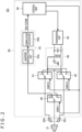
- FIG. 2 is a diagram illustrating an internal configuration of the active pen 2C.
- the active pen 2C configurations of the active pens 2A and 2B will also be mentioned.
- the pen tip electrode 21 is a conductor that plays a role of an antenna for transmitting a downlink signal DS and that also plays a role of an antenna for receiving a beacon signal BS transmitted by the sensor controller 31 through the sensor electrode group 30. Note that a member that provides the pen tip may be arranged separately from the pen tip electrode 21. In addition, an electrode that receives the beacon signal BS may be arranged separately from the pen tip electrode 21.
- the peripheral electrodes 22b and 22c are conductors that play a role of antennas for transmitting the downlink signal DS.
- the signal processing unit 20 can transmit the downlink signal DS or a reverse-phase signal of the downlink signal DS from each of the peripheral electrodes 22b and 22c. In other words, the signal processing unit 20 can individually switch each of the peripheral electrodes 22b and 22c to transmit the downlink signal DS or to transmit the reverse-phase signal of the downlink signal DS.
- the signal processing unit 20 has a function of starting or stopping the downlink signal DS or the reverse-phase signal of the downlink signal DS from each of the pen tip electrode 21 and the peripheral electrodes 22b and 22c according to a predetermined trigger.
- the predetermined trigger is provided by the beacon signal BS transmitted by the sensor controller 31. More specifically, the signal processing unit 20 starts or stops the downlink signal DS or the reverse-phase signal of the downlink signal DS from each of the pen tip electrode 21 and the peripheral electrodes 22b and 22c according to a transmission schedule indicated by setting information (described later) arranged in the beacon signal BS.
- the signal processing unit 20 includes functional units including switching units 40 to 42, a detection unit 43, a control unit 44, a transmission unit 45, and a reverse-phase signal generation unit 46.
- the functional units will be sequentially described.
- the switching unit 40 is a single-pole double-throw switching element in which a common terminal and any one of a T terminal and an R terminal are connected.
- the common terminal of the switching unit 40 is connected to the pen tip electrode 21.
- the T terminal is connected to a normal-phase signal output terminal of the reverse-phase signal generation unit 46, and the R terminal is connected to an input terminal of the detection unit 43.
- the state of the switching unit 40 is controlled by a control signal SWC1 from the control unit 44.
- the control unit 44 uses the control signal SWC1 to control the switching unit 40 to connect the R terminal and the common terminal.
- the control unit 44 uses the control signal SWC1 to control the switching unit 40 to connect the T terminal and the common terminal.
- the switching unit 41 is a single-pole double-throw switching element in which a common terminal and any one of a positive terminal and a negative terminal are connected.
- the common terminal of the switching unit 41 is connected to the peripheral electrode 22b.
- the positive terminal is connected to the normal-phase signal output terminal of the reverse-phase signal generation unit 46, and the negative terminal is connected to a reverse-phase signal output terminal of the reverse-phase signal generation unit 46.
- the state of the switching unit 41 is controlled by a control signal SWC2 from the control unit 44.
- the control unit 44 uses the control signal SWC2 to control the switching unit 41 to connect the positive terminal and the common terminal.
- the control unit 44 uses the control signal SWC2 to control the switching unit 41 to connect the negative terminal and the common terminal.
- the switching unit 42 is a single-pole double-throw switching element in which a common terminal and any one of a positive terminal and a negative terminal are connected.
- the common terminal of the switching unit 42 is connected to the peripheral electrode 22c.
- the positive terminal is connected to the normal-phase signal output terminal of the reverse-phase signal generation unit 46, and the negative terminal is connected to the reverse-phase signal output terminal of the reverse-phase signal generation unit 46.
- the state of the switching unit 42 is controlled by a control signal SWC3 from the control unit 44.
- the control unit 44 uses the control signal SWC3 to control the switching unit 42 to connect the positive terminal and the common terminal.
- the control unit 44 uses the control signal SWC3 to control the switching unit 42 to connect the negative terminal and the common terminal.
- the active pen 2A does not include the switching units 41 and 42 and the reverse-phase signal generation unit 46, and an output terminal of the transmission unit 45 is directly connected to the T terminal of the switching unit 40.
- the active pen 2B does not include the switching unit 42, and the common terminal of the switching unit 41 is connected to the peripheral electrode 22a.
- the detection unit 43 is a circuit that detects a signal supplied from the switching unit 40 (signal arriving at the pen tip electrode 21) and that decodes a code sequence included in the detected signal.
- the detection unit 43 includes a waveform reproduction unit 43a and a correlation calculator 43b. Through the decoding, the detection unit 43 can detect the beacon signal BS.
- the waveform reproduction unit 43a binarizes the level of the charge (voltage) induced to the pen tip electrode 21 by using a clock at a rate several times (for example, four times) the chip rate of the spreading code used by the sensor controller 31 to spread the beacon signal BS.
- the waveform reproduction unit 43a shapes a binary sequence (chip sequence) of positive and negative polarity values and outputs the binary sequence.
- the correlation calculator 43b stores the chip sequence output by the waveform reproduction unit 43a in a register and performs a correlation operation with each of a plurality of spreading codes that may be transmitted by the sensor controller 31 while using the clock to sequentially shift the chip sequence. In this way, the correlation calculator 43b decodes the chip sequence included in the reception signal into a format of symbols.
- the symbol is a unit of information associated with one spreading code, and the symbols include a symbol D corresponding to the bit sequence and a symbol P not corresponding to the bit sequence.
- the beacon signal BS includes a preamble PRE for causing the active pen 2 to detect the beacon signal BS and a command COM indicating an instruction for the active pens 2, and the preamble PRE and the command COM are included in this order.
- the preamble PRE includes two consecutive symbols P
- the command COM includes four consecutive symbols D.
- the detection unit 43 successively performs a detection operation of the preamble PRE based on the decoding result of the correlation calculator 43b.
- the detection operation is an operation for determining whether or not two consecutive symbols P are acquired.
- the detection unit 43 detects the existence of the sensor controller 31 by detecting the preamble PRE
- the detection unit 43 issues, to the control unit 44, a start signal EN for starting the control unit 44 and then performs a detection operation of the command COM.
- the detection unit 43 sequentially demodulates the series of symbols D, which are sequentially obtained by decoding, to a bit sequence.
- the detection unit 43 ultimately obtains a bit sequence of a predetermined number of bits and outputs the bit sequence to the control unit 44.
- the transmission unit 45 is a circuit that generates the downlink signal DS according to the control of the control unit 44 and that supplies the downlink signal DS to the reverse-phase signal generation unit 46.
- the downlink signal DS generated by the transmission unit 45 includes a response signal transmitted just after the reception of the beacon signal BS and an in-slot signal transmitted in a time slot described later.
- the response signal includes a burst signal, which is a non-modulated carrier signal, and a data signal, which is a carrier signal modulated based on data transmitted by the active pen 2C to the sensor controller 31.
- the data transmitted to the sensor controller 31 includes functional information indicating the number, the shape, and the arrangement of electrodes provided on the active pen 2C.
- the in-slot signal includes a burst signal that is a non-modulated carrier signal.
- the reverse-phase signal generation unit 46 is a circuit that generates a reverse-phase signal obtained by inverting the phase of the downlink signal DS.
- the reverse-phase signal generation unit 46 includes the normal-phase signal output terminal that outputs the downlink signal DS and the reverse-phase signal output terminal that outputs the reverse-phase signal of the downlink signal DS.
- the control unit 44 includes a read-only memory (ROM) and a random-access memory (RAM) inside and is a microprocessor that operates by executing programs stored in the ROM and the RAM.
- the control unit 44 is activated by the supply of the start signal EN from the detection unit 43.
- the activated control unit 44 performs an operation according to the command COM supplied from the detection unit 43.
- the operation includes a process of outputting the downlink signal DS to the transmission unit 45 and a process of using the control signals SWC1 to SWC3 to control the switching units 40 to 42.
- the control unit 44 stores a flag that is true when the sensor controller 31 is detected and that is false when the sensor controller 31 is not detected.
- the control unit 44 receiving the command COM when the flag is false transmits a response signal from the pen tip electrode 21 just after the start signal EN is supplied from the detection unit 43.
- the control unit 44 causes the transmission unit 45 to output the response signal and uses the control signals SWC1 to SWC3 to connect the pen tip electrode 21 to the normal-phase signal output terminal of the reverse-phase signal generation unit 46.
- the control unit 44 can transmit the response signal in this way to cause the sensor controller 31 to detect the active pen 2C and notify the sensor controller 31 of the functional information of the active pen 2C.
- the control unit 44 rewrites the flag to true along with the transmission of the response signal.
- the sensor controller 31 when the sensor controller 31 correctly receives the response signal transmitted by the active pen 2C, the sensor controller 31 acquires the number, the shape, and the arrangement of electrodes included in the active pen 2C from the functional information included in the response signal. Furthermore, based on the acquired information, the sensor controller 31 allocates one or more time slots to each electrode and determines the type of signal (downlink signal DS or reverse-phase signal of downlink signal DS) to be transmitted by the active pen 2C from each electrode.
- the command COM in the beacon signal BS includes setting information indicating results of the allocation and the determination.
- the control unit 44 When the control unit 44 receives the command COM after storing the flag in the memory, the control unit 44 acquires, for each electrode, the transmission timing of the downlink signal DS or the reverse-phase signal of the downlink signal DS from the setting information included in the command COM. Furthermore, the control unit 44 transmits the in-slot signal or a reverse-phase signal of the in-slot signal from at least one of the pen tip electrode 21 and the peripheral electrodes 22b and 22c according to the acquired transmission timing. Specifically, to transmit the in-slot signal from an electrode, the control unit 44 causes the transmission unit 45 to output the in-slot signal and uses the control signals SWC1 to SWC3 to connect the electrode to the normal-phase signal output terminal of the reverse-phase signal generation unit 46.
- control unit 44 causes the transmission unit 45 to output the in-slot signal and uses the control signals SWC1 to SWC3 to connect the electrode to the reverse-phase signal output terminal of the reverse-phase signal generation unit 46.
- FIG. 3 is a diagram illustrating internal configurations of the sensor electrode group 30 and the sensor controller 31.
- the sensor electrode group 30 provides a mutual-capacitance touch sensor and includes the plurality of sensor electrodes 30X and the plurality of sensor electrodes 30Y arranged in a matrix, in which the plurality of sensor electrodes 30X are transparent conductors extending in a Y-direction and arranged at equal intervals in an X-direction orthogonal to the Y-direction, and the plurality of sensor electrodes 30Y are transparent conductors extending in the X-direction and arranged at equal intervals in the Y-direction.
- the sensor electrodes 30X and 30Y include linear conductors in the example illustrated here, conductors in other shapes can be included in the sensor electrode group 30. For example, a plurality of two-dimensionally arranged rectangular conductors may be included in the sensor electrode group 30.
- the sensor electrode group 30 may provide a self-capacitance touch sensor instead of the mutual-capacitance touch sensor.
- One of the sensor electrodes 30X and 30Y may also be used as common electrodes in the display apparatus.
- the type of tablet terminal 3 in which one of the sensor electrodes 30X and 30Y is used as common electrodes in the display apparatus is called, for example, an "in-cell type.”
- the type of tablet terminal 3 in which the sensor electrodes 30X and 30Y and the common electrodes in the display apparatus are separately provided is called, for example, an "out-cell type” or an "on-cell type.”
- the description will be continued by assuming that the tablet terminal 3 is the in-cell type, the present invention can be similarly applied to the out-cell type or on-cell type tablet terminal.
- the sensor electrodes 30Y may be used as the common electrodes.
- the display apparatus needs to maintain the potential of the common electrodes at a predetermined common potential Vcom to execute the driving process of pixels. Therefore, in the in-cell type tablet terminal 3, the sensor controller 31 cannot communicate with the active pens 2A to 2C or detect the finger while the display apparatus is executing the driving process of pixels. Therefore, the host processor 32 uses a horizontal blanking interval and a vertical blanking interval in which the driving process of pixels is not executed and causes the sensor controller 31 to communicate with the active pen 2 and detect the finger. Specifically, the host processor 32 sets the display period corresponding to one screen as one frame and regards the horizontal blanking interval and the vertical blanking interval included in the frame as time slots to control the sensor controller 31 to communicate with the active pen 2 and detect the finger within individual time slots.
- the sensor controller 31 includes a memory control unit (MCU) 50, a logic unit 51, transmission units 52 and 53, a reception unit 54, and a selection unit 55 as illustrated in FIG. 3 .
- MCU memory control unit
- the MCU 50 and the logic unit 51 are control units that control the transmission units 52 and 53, the reception unit 54, and the selection unit 55 to control transmission and reception operations of the sensor controller 31.
- the MCU 50 includes a ROM and a RAM inside and is a microprocessor that operates by executing programs stored in the ROM and the RAM.
- the MCU 50 also has a function of outputting the common potential Vcom and the command COM.
- the logic unit 51 is configured to output control signals ctrl_t1 to ctrl_t4, ctrl_r, sTRx, sTRy, selX, and selY based on the control of the MCU 50.
- the order based on the command COM output by the MCU 50 includes the setting information indicating the allocation of one or more time slots for each electrode included in each of the detected active pens 2 and indicating the type of signal (downlink signal DS or reverse-phase signal of downlink signal DS) to be transmitted by the active pen 2 from each electrode in the allocated time slots.
- the MCU 50 is configured to select one of a plurality of pieces of predefined setting information described later for each of the active pens 2 and to arrange, in the command COM, one or more indices respectively indicating one or more pieces of selected setting information.
- the order based on the command COM may also include transmission of pen pressure data indicating the pressure applied to the pen tip of the active pen 2, transmission of data indicating the pressed state of a switch (not illustrated) provided on the surface of the active pen 2, transmission of a stylus identification (ID) stored in advance in the active pen 2, and the like.
- the active pen 2 receiving the orders may include the instructed data in the data signal of the response signal to transmit the data or may use short-range wireless communication, such as Bluetooth (registered trademark), to transmit the data.
- the in-slot signal to be transmitted from the pen tip electrode 21 may be provided as a signal modulated by the instructed data to thereby transmit the instructed data.
- the transmission unit 52 is a circuit that generates a finger detection signal FDS used for detecting the finger according to the control of the MCU 50.
- the finger detection signal FDS may be, for example, a non-modulated pulse sequence signal or a sinusoidal signal.
- the transmission unit 53 is a circuit that generates the beacon signal BS according to the control of the MCU 50 and the logic unit 51, and the transmission unit 53 includes a preamble supply unit 61, a switch 62, a code sequence holding unit 63, a spread processing unit 64, and a transmission guard unit 65 as illustrated in FIG. 2 . Note that among these, the preamble supply unit 61 may be included in the MCU 50.
- the preamble supply unit 61 holds the preamble PRE and has a function of outputting the preamble PRE according to an instruction of the control signal ctrl_t1 supplied from the logic unit 51.
- the preamble PRE output by the preamble supply unit 61 is supplied to the switch 62.
- the command COM is also supplied from the MCU 50 to the switch 62.
- the switch 62 has a function of selecting any one of the preamble supply unit 61 and the MCU 50 according to the control signal ctrl_t2 supplied from the logic unit 51 and supplying the output of the selected one to the spread processing unit 64.
- the switch 62 selects the preamble supply unit 61, two symbols P included in the preamble PRE are sequentially supplied to the spread processing unit 64.
- the switch 62 selects the MCU 50, four symbols D included in the command COM are sequentially supplied to the spread processing unit 64.
- the code sequence holding unit 63 has a function of generating and holding a spreading code with autocorrelation properties, with a length of, for example, 11 chips, based on the control signal ctrl_t3 supplied from the logic unit 51.
- the spreading code held by the code sequence holding unit 63 is supplied to the spread processing unit 64.
- the spread processing unit 64 has a function of modulating the spreading code held by the code sequence holding unit 63 based on the values of the symbols supplied through the switch 62.
- the modulation is performed by, for example, a cyclic shift, and in that case, a spreading code with a length of 12 chips is output for each symbol as a result of the modulation.
- the spreading codes output from the spread processing unit 64 are sequentially supplied to the transmission guard unit 65.
- the transmission guard unit 65 plays a role of inserting a guard period, which is a period in which both of the transmission and the reception are not performed, between a transmission period of the beacon signal BS and a period of a reception operation performed by the reception unit 54 described later based on the control signal ctrl_t4 supplied from the logic unit 51.
- the reception unit 54 is a circuit for receiving the downlink signal DS transmitted by the active pen 2 or the finger detection signal FDS transmitted by the transmission unit 52 based on the control signal ctrl_r of the logic unit 51.
- the reception unit 54 includes an amplifier circuit 70, a detection circuit 71, and an analog-digital (AD) converter 72.
- the amplifier circuit 70 amplifies and outputs the signal supplied from the selection unit 55.
- the detection circuit 71 is a circuit that generates a voltage corresponding to the level of the output signal of the amplifier circuit 70.
- the AD converter 72 is a circuit that samples, at predetermined time intervals, the voltage output from the detection circuit 71 to thereby generate a digital signal.
- the digital signal output by the AD converter 72 is supplied to the MCU 50. Based on the digital signal supplied in this way, the MCU 50 detects the position (x, y) of the active pen 2 or the finger, the inclination ⁇ and the azimuth ⁇ of the active pens 2B and 2C, and the rotation angle ⁇ of the active pen 2C and acquires data Res transmitted by the active pen 2.
- the MCU 50 successively outputs the detected position (x, y), inclination ⁇ , azimuth ⁇ , and rotation angle ⁇ and the acquired data Res to the host processor 32.
- the selection unit 55 includes switches 68x and 68y and conductor selection circuits 69x and 69y.
- the switch 68y is a switching element in which a common terminal and any one of a T terminal and an R terminal are connected.
- the common terminal of the switch 68y is connected to the conductor selection circuit 69y.
- the T terminal is connected to an output terminal of the transmission unit 53, and the R terminal is connected to an input terminal of the reception unit 54.
- the switch 68x is a switching element in which a common terminal and any one of a T1 terminal, a T2 terminal, a D terminal, and an R terminal are connected.
- the common terminal of the switch 68x is connected to the conductor selection circuit 69x.
- the T1 terminal is connected to the output terminal of the transmission unit 53.
- the T2 terminal is connected to an output terminal of the transmission unit 52.
- the D terminal is connected to an output terminal of the MCU 50 that outputs the common potential Vcom.
- the R terminal is connected to the input terminal of the reception unit 54.
- the conductor selection circuit 69x is a switching element for selectively connecting the plurality of sensor electrodes 30X to the common terminal of the switch 68x.
- the conductor selection circuit 69x can also connect part or all of the plurality of sensor electrodes 30X to the common terminal of the switch 68x at the same time.
- the conductor selection circuit 69y is a switching element for selectively connecting the plurality of sensor electrodes 30Y to the common terminal of the switch 68y.
- the conductor selection circuit 69y can also connect part or all of the plurality of sensor electrodes 30Y to the common terminal of the switch 68y at the same time.
- control signals sTRx, sTRy, selX, and selY are supplied from the logic unit 51 to the selection unit 55.
- the control signal sTRx is supplied to the switch 68x.
- the control signal sTRy is supplied to the switch 68y.
- the control signal selX is supplied to the conductor selection circuit 69x.
- the control signal selY is supplied to the conductor selection circuit 69y.
- the logic unit 51 uses the control signals sTRx, sTRy, selX, and selY to control the selection unit 55 to realize the transmission of the beacon signal BS or the finger detection signal FDS, the application of the common potential Vcom, and the reception of the downlink signal DS or the finger detection signal FDS.
- the logic unit 51 in detecting the finger controls the switch 68x to connect the T2 terminal to the common terminal and controls the switch 68y to connect the R terminal to the common terminal. Furthermore, the logic unit 51 controls the conductor selection circuits 69x and 69y to sequentially select the combinations of the plurality of sensor electrodes 30X and 30Y In this way, the finger detection signals FDS passing through a plurality of intersections of the plurality of sensor electrodes 30X and 30Y are sequentially received by the reception unit 54.
- the MCU 50 detects the position of the finger on the panel surface 3a based on the reception intensity of the finger detection signals FDS sequentially received in this way.
- the logic unit 51 in executing the pixel driving operation controls the switch 68x to connect the D terminal to the common terminal and controls the conductor selection circuit 69x to connect all of the plurality of sensor electrodes 30X to the switch 68x at the same time.
- the common potential Vcom is supplied from the MCU 50 to each sensor electrode 30X, and the display apparatus can execute the pixel driving operation.
- the MCU 50 causes the logic unit 51 to execute the control at timing based on a timing signal supplied from the host processor 32.
- the logic unit 51 in transmitting the beacon signal BS controls the switch 68x to connect the R terminal to the common terminal and controls the switch 68y to connect the T terminal to the common terminal.
- the beacon signal BS output from the transmission unit 53 is supplied to the conductor selection circuit 69y.
- the logic unit 51 further controls the conductor selection circuit 69y to connect all of the plurality of sensor electrodes 30Y to the switch 68y at the same time.
- the beacon signals BS are transmitted from all of the sensor electrodes 30Y at the same time, and the active pen 2 can receive the beacon signal BS anywhere in the panel surface 3 a.
- the logic unit 51 in receiving the response signal controls each of the switches 68x and 68y to connect the R terminal to the common terminal. Furthermore, the logic unit 51 first executes a process of using the control signals selX and selY to control the conductor selection circuits 69x and 69y to sequentially select the plurality of sensor electrodes 30X and 30Y one by one while the burst signal in the response signal is transmitted. As a result, the plurality of sensor electrodes 30X and 30Y are sequentially connected to the input terminal of the reception unit 54 one by one, and the reception intensity of the burst signal in each of the sensor electrodes 30X and 30Y is sequentially supplied from the reception unit 54 to the MCU 50.
- the MCU 50 determines the position of the active pens 2 that has transmitted the response signal, based on the series of reception intensity supplied in this way.
- the logic unit 51 controls the conductor selection circuits 69x and 69y to select only a predetermined number (for example, one) of the plurality of sensor electrodes 30X and 30Y near the detected position.
- the response signals received by the selected predetermined number of sensor electrodes are supplied to the MCU 50 through the reception unit 54.
- the data signal transmitted after the burst signal is supplied to the MCU 50.
- the MCU 50 demodulates and decodes the data signal supplied in this way to acquire the data Res.
- the logic unit 51 in receiving the in-slot signal controls each of the switches 68x and 68y to connect the R terminal to the common terminal and then executes a process of using the control signals selX and selY to control the conductor selection circuits 69x and 69y to sequentially select a predetermined number (for example, five) of the plurality of sensor electrodes 30X positioned near the latest position detected for the corresponding active pens 2 and a predetermined number (for example, five) of the plurality of sensor electrodes 30Y positioned near the latest position detected for the corresponding active pen 2.
- a predetermined number for example, five
- the selected sensor electrodes 30X and 30Y are sequentially connected to the input terminal of the reception unit 54 one by one, and the reception intensity of the in-slot signal in each of the sensor electrodes 30X and 30Y is sequentially supplied from the reception unit 54 to the MCU 50.
- the MCU 50 updates the position (x, y) of the active pen 2 that has transmitted the in-slot signal, detects the inclination ⁇ and the azimuth ⁇ , and detects the rotation angle ⁇ .
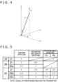
- FIG. 4 is an explanatory view of the inclination ⁇ , the azimuth ⁇ , and the rotation angle ⁇ of the active pen 2.
- the X-axis and the Y-axis indicate directions on the panel surface 3a
- the Z-axis indicates the normal direction of the panel surface 3a.
- the thick line represents the pen axis of the active pen 2
- a position P indicates the contact position of the pen tip of the active pen 2 and the panel surface 3a.
- the inclination ⁇ of the active pen 2 is expressed by an angle formed by the Z-axis and the pen axis of the active pen 2.
- T represents a position of intersection between a perpendicular line, which is drawn from one point on the pen axis to the XY plane, and the XY plane
- the azimuth ⁇ of the active pens 2 is expressed by an angle formed by a line segment, which connects the position P and the position T, and the X-axis.
- the rotation angle ⁇ denotes a rotation angle of the active pen 2 about the pen axis.
- FIG. 5 is a diagram illustrating in-slot signals to be transmitted by the active pen 2, the transmission of which is ordered by the sensor controller 31, in each of the case of detecting the position (x, y), the case of detecting the inclination ⁇ and the azimuth ⁇ , and the case of detecting the rotation angle ⁇ .
- "+” denotes transmission of a normal-phase signal of the in-slot signal (burst signal) output from the transmission unit 45 illustrated in FIG. 2
- "-" denotes transmission of a reverse-phase signal of the in-slot signal (burst signal) output from the transmission unit 45 illustrated in FIG. 2 .
- the active pens 2A corresponds to only the detection of the position (x, y) and does not correspond to the detection of the inclination ⁇ , the azimuth ⁇ , and the rotation angle ⁇ .
- the sensor controller 31 In detecting the position (x, y) of the active pen 2A, the sensor controller 31 causes the active pens 2A to transmit the normal-phase signal of the in-slot signal from the pen tip electrode 21.
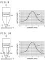
- FIG. 9 is a diagram illustrating a reception intensity distribution on the panel surface 3a when the active pen 2A transmits the burst signal from the pen tip electrode 21.
- a coordinate 0 represents the contact position of the pen tip electrode 21 and the panel surface 3a.
- a broken-line graph indicates a case in which the angle formed by the panel surface 3a and the pen axis is 0 degrees (case in which active pen 2A is upright with respect to panel surface 3a), and a solid-line graph indicates a case in which the angle formed by the panel surface 3a and the pen axis is 45 degrees (case in which active pen 2A is tilted with respect to panel surface 3a).
- the reception intensity distribution of the case in which the active pen 2A is upright with respect to the panel surface 3a is a substantially normal distribution with the peak at the contact position (coordinate 0) of the pen tip electrode 21 and the panel surface 3 a.
- the sensor controller 31 uses such a property of the reception intensity distribution to calculate the position (x, y) of the active pen 2A. Specifically, the sensor controller 31 uses the normal distribution curve to approximate the reception intensity in each of the predetermined number of sensor electrodes 30X and obtains the peak position to thereby calculate the x-coordinate at the position of the active pen 2A. In addition, the sensor controller 31 uses the normal distribution curve to approximate the reception intensity in each of the predetermined number of sensor electrodes 30Y and obtains the peak position to thereby calculate the y-coordinate at the position of the active pen 2A.
- the peak of the reception intensity distribution of the case in which the active pen 2A is tilted with respect to the panel surface 3a is moved toward the tilt of the active pen 2A compared to the case where the active pen 2A is upright.
- the position (x, y) of the active pens 2A calculated as described above is also shifted toward the tilt of the active pen 2A as viewed from the original contact position.
- the peripheral electrodes 22a to 22c can be used to reduce the positional shift in the active pens 2B and 2C.
- the active pen 2B corresponds to the detection of the position (x, y), the inclination ⁇ , and the azimuth ⁇ and does not correspond to the detection of the rotation angle ⁇ as illustrated in FIG. 5 .
- the sensor controller 31 causes the active pen 2B to transmit the normal-phase signal of the in-slot signal from the pen tip electrode 21 and causes the active pen 2B to transmit the reverse-phase signal of the in-slot signal from the peripheral electrode 22a at the same time.
- the sensor controller 31 causes the active pen 2B to transmit the normal-phase signals of the in-slot signals from the pen tip electrode 21 and the peripheral electrode 22a at the same time.
- FIG. 10 is a diagram illustrating a reception intensity distribution on the panel surface 3a when the active pen 2B transmits the burst signal from the pen tip electrode 21 and transmits the reverse-phase signal of the burst signal from the peripheral electrode 22a at the same time.
- the specific method of calculating the position (x, y) of the active pen 2B performed by the sensor controller 31 based on the reception intensity illustrated in FIG. 10 is similar to the case of the active pen 2A.
- the positional shift of the peak in the solid-line graph is smaller in the example of FIG. 10 than in the example of FIG. 9 .
- the transmission of the burst signal from the pen tip electrode 21 and the transmission of the reverse-phase signal of the burst signal from the peripheral electrode 22a at the same time selectively reduce the intensity of the downlink signal DS in the direction of the tilt of the active pen 2B. Therefore, even when the active pen 2B is tilted with respect to the panel surface 3a, the sensor controller 31 can correctly detect the instruction position compared to the case of the active pens 2A.
- the signal may not be transmitted from the peripheral electrode 22a in detecting the position (x, y) of the active pen 2B. Even in this way, the position (x, y) of the active pen 2B can also be detected with accuracy at least equivalent to the accuracy of the active pen 2A.
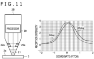
- FIG. 11 is a diagram illustrating a reception intensity distribution on the panel surface 3a when the active pen 2B transmits the burst signal from each of the pen tip electrode 21 and the peripheral electrode 22a.
- the positional shift of the peak of the reception intensity distribution in the case where the active pen 2B is tilted with respect to the panel surface 3a is larger in the example of FIG. 11 than in the case of FIG. 10 . This is because the tilt of the active pen 2B significantly changes the position of the peripheral electrode 22a.
- the sensor controller 31 uses such a property of the reception intensity distribution to calculate the inclination ⁇ and the azimuth ⁇ of the active pen 2B.
- FIG. 6 is a diagram illustrating a principle of calculating the inclination ⁇ and the azimuth ⁇ of the active pen 2B.
- the position T illustrated in FIG. 6 indicates the position of the active pen 2B detected when the active pen 2B transmits the in-slot signals from the pen tip electrode 21 and the peripheral electrode 22a at the same time.
- the sensor controller 31 first calculates the distance d and applies the result of the calculation to the equation to calculate the angle ⁇ .
- the sensor controller 31 obtains an angle formed by a vector from the position P toward the position T and the X-axis to calculate the azimuth ⁇ . In this way, the sensor controller 31 is configured to use the position P and the position T to calculate the inclination ⁇ and the azimuth ⁇ of the active pen 2B.
- the signal may not be transmitted from the pen tip electrode 21 in detecting the inclination ⁇ and the azimuth ⁇ of the active pen 2B.
- the distance d can be a larger value, and the angle ⁇ can be calculated with higher accuracy.
- the active pen 2C corresponds to the detection of all of the position (x, y), the inclination ⁇ , the azimuth ⁇ , and the rotation angle ⁇ as illustrated in FIG. 5 .
- the signals transmitted from the electrodes in detecting the position (x, y) of the active pen 2C and in detecting the inclination ⁇ and the azimuth ⁇ of the active pen 2C are similar to the case of the active pen 2B.
- the signals transmitted from the peripheral electrodes 22b and 22c are the same as the signals transmitted from the peripheral electrode 22a of the active pen 2B.
- step R1 The signal transmission in detecting the rotation angle ⁇ of the active pen 2C is executed in two steps R1 and R2.
- step R1 the sensor controller 31 causes the active pen 2C to transmit the in-slot signals from the pen tip electrode 21 and the peripheral electrode 22b at the same time, and at the same time, transmit the reverse-phase signal of the in-slot signal from the peripheral electrode 22c.
- step R2 the sensor controller 31 causes the active pen 2C to transmit the in-slot signals from the pen tip electrode 21 and the peripheral electrode 22c at the same time, and at the same time, transmit the reverse-phase signal of the in-slot signal from the peripheral electrode 22b.
- the reception intensity distribution on the panel surface 3a in detecting the position (x, y) is similar to the reception intensity distribution in FIG. 10 .
- the sensor controller 31 calculates the position (x, y) of the active pen 2C as in the case of the active pen 2B. As a result, even when the active pen 2C is tilted with respect to the panel surface 3a, the sensor controller 31 can correctly detect the instruction position of the active pen 2C compared to the case of the active pen 2A.
- the reception intensity distribution on the panel surface 3a in detecting the inclination ⁇ and the azimuth ⁇ is similar to the reception intensity distribution in FIG. 11 .
- the sensor controller 31 calculates the inclination ⁇ and the azimuth ⁇ as in the case of the active pen 2B.
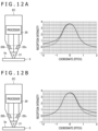
- FIG. 12A is a diagram illustrating the reception intensity distribution on the panel surface 3a in step R1 illustrated in FIG. 5 .
- FIG. 12B is a diagram illustrating the reception intensity distribution on the panel surface 3a in step R2 illustrated in FIG. 5 .
- the inclination ⁇ of the active pen 2C is 0 degrees.
- the broken-line graph in the case of 0 degrees in FIG. 10 is illustrated again for comparison.
- the reception intensity on the side of one of the peripheral electrodes 22b and 22c that transmits the normal-phase signal of the burst signal is larger than the reception intensity on the side of the other of the peripheral electrodes 22b and 22c that transmits the reverse-phase signal of the burst signal.
- the sensor controller 31 uses such a property of the reception intensity distribution to calculate the rotation angle ⁇ of the active pen 2C.
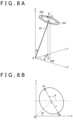
- FIG. 7 and FIG. 8 illustrate a principle of calculating the rotation angle ⁇ of the active pen 2C.
- FIG. 7 illustrates a case in which the inclination ⁇ is 0, and
- FIG. 8 illustrates a case in which the inclination ⁇ is not 0.
- Positions R1 and R2 illustrated in FIGS. 7 and 8 indicate positions detected in steps R1 and R2 illustrated in FIG. 5 , respectively.
- FIGS. 12A and 12B although the actual position of the peak of the reception intensity distribution is about the same in step R1 and step R2, the position of the peak obtained by approximation using the normal distribution curve significantly varies between step R1 and step R2 due to the bias. Therefore, as illustrated in FIGS.
- the position R1 detected in step R1 and the position R2 detected in step R2 are significantly different.
- the position R1 and the position R2 are at positions symmetric about the position P when the inclination ⁇ is 0 and are at positions symmetric about the position T when the inclination ⁇ is not 0.
- the position R1 is a position detected when the peripheral electrode 22b transmits the normal-phase signal of the burst signal, and therefore, the position R1 corresponds to the side provided with the peripheral electrode 22b in the periphery of the active pen 2C.
- the position R2 is a position detected when the peripheral electrode 22c transmits the normal-phase signal of the burst signal, and therefore, the position R2 corresponds to the side provided with the peripheral electrode 22c in the periphery of the active pen 2C. Therefore, it can be stated that an angle formed by a vector v (vector from position R2 toward position R1) and the X-axis illustrated in FIG. 7(b) and FIG. 8(b) corresponds to the rotation angle ⁇ of the active pen 2C.
- the sensor controller 31 obtains the angle formed by the vector v and the X-axis to calculate the rotation angle ⁇ . In this way, the sensor controller 31 is configured to use the position R1 and the position R2 to calculate the rotation angle ⁇ of the active pen 2C.
- the signal may not be transmitted from the pen tip electrode 21 in detecting the rotation angle ⁇ of the active pen 2C. Furthermore, instead of transmitting the reverse-phase signal, a signal may not be transmitted. Even in this way, the position R1 and the position R2 can be used to calculate the rotation angle ⁇ of the active pen 2C as described above.
- the intensity of the downlink signal DS in the direction of the tilt of the active pens 2B and 2C can be selectively reduced. Therefore, the sensor controller 31 can correctly detect the instruction positions of the active pens 2B and 2C tilted with respect to the panel surface 3a.
- the inclination ⁇ and the azimuth ⁇ can be calculated in addition to the instruction position. Furthermore, according to the active pen 2C of the present embodiment, the rotation angle ⁇ can be further calculated.
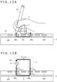
- FIG. 13A is a diagram illustrating a state in which the user uses the active pen 2A to write on the panel surface 3a of the tablet terminal 3.
- FIG. 13B is a diagram illustrating an equivalent circuit of FIG. 13A . Note that the pictures of the tablet terminal 3 illustrated in FIGS. 13A and 13B are cross-sectional views schematically illustrating a cross section cut in the X-direction.
- a sensor electrode 30X 1 illustrated in FIG. 13A represents the sensor electrode 30X closest to the pen tip electrode 21.
- a sensor electrode 30X 2 illustrated in FIG. 13A represents the sensor electrode 30X closest to the hand of the user holding the active pen 2A. Note that in the example of FIG. 13A , the hand of the user holding the active pen 2 is touching the panel surface 3a near the sensor electrode 30X 2 .
- Capacitance C pen_tip illustrated in FIG. 13B is coupling capacitance formed between the pen tip electrode 21 of the active pen 2A and the sensor electrode 30X 1 .
- capacitance C pen_GND is coupling capacitance formed between a housing (ground terminal) of the active pen 2A and the hand of the user
- capacitance C palm is coupling capacitance formed between the hand of the user touching the panel surface 3a and the sensor electrode 30X 2 .
- capacitance C X_Y is coupling capacitance formed between each sensor electrode 30X and a sensor electrode 30Y
- a current path A is formed from the pen tip electrode 21 to the sensor electrode 30Y through the sensor electrode 30X 1 and further from the sensor electrode 30Y to the ground terminal of the active pen 2A through the sensor electrode 30X 2 and a human body 4.
- part of the downlink signal DS sent out from the pen tip electrode 21 of the active pen 2A flows through the current path A, and at that time, a current is induced in the sensor electrode 30X 2 .
- the sensor controller 31 also detects the pen tip electrode 21 of the active pen 2A near the sensor electrode 30X 2 . This is the reason that the sensor controller 31 falsely detects the contact position of the hand as the instruction position of the active pen 2.
- the active pens 2B and 2C according to the present embodiment can be used to prevent such a false detection. This will be described in detail with reference to FIG. 14 .
- FIG. 14 is a diagram illustrating an equivalent circuit similar to FIG. 13B regarding the case in which the active pen 2B transmits the reverse-phase signal of the downlink signal DS from the peripheral electrode 22a. As indicated by parentheses in FIG. 14 , the equivalent circuit is also similar in the case where the active pen 2C transmits the reverse-phase signals of the downlink signals DS from the peripheral electrodes 22b and 22c.
- the reverse-phase signal of the downlink signal DS can be transmitted from the peripheral electrode at the same time as the transmission of the downlink signal DS from the pen tip electrode, and this allows the peripheral electrode to absorb the downlink signal DS originally absorbed by the hand of the user. This prevents the sensor controller 31 from falsely detecting the contact position of the hand as the instruction position of the active pen 2.
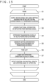
- FIG. 15 is a flow chart illustrating a flow of the sensor controller 31 according to the present embodiment. As illustrated in FIG. 15 , the sensor controller 31 is configured to repeat processes of steps S2 to S7 for each frame including a plurality of time slots (step S1).
- step S2 the sensor controller 31 supplies the beacon signal BS as reference time of the frame to the sensor electrode group 30 (beacon signal supply step). At this point, the sensor controller 31 arranges, in the beacon signal BS, the setting information of each active pen 2 necessary for executing the transmission schedule determined in step S4 of the previous cycle. As a result, the setting information is transmitted to each of one or more active pens 2 detected by the sensor controller 31 (setting step).
- the sensor controller 31 then detects the response signal returned by the active pen 2 in response to the beacon signal BS and acquires the functional information of the active pen 2 from the response signal (step S3, functional information acquisition step). In addition, the sensor controller 31 determines the transmission schedule of each active pen 2 based on the functional information of each of one or more detected active pens 2 including the active pen 2 for which the functional information is newly acquired (step S4).
- the determination includes determination of the type of detection operation (one or more of position detection, inclination and azimuth detection, and rotation angle detection) executed for each active pen 2, allocation of one or more time slots to each electrode based on the result of the determination of the type of detection operation, and determination of the type of signal (downlink signal DS or reverse-phase signal of downlink signal DS) to be transmitted by the active pen 2 from each electrode in the allocated time slots.
- the type of detection operation one or more of position detection, inclination and azimuth detection, and rotation angle detection
- the execution of the position detection and the inclination and azimuth detection is determined for the active pen 2 (for example, active pen 2B) with functional information indicating that the peripheral electrode is isotropic with respect to the rotation about the pen axis
- the execution of the position detection, the inclination and azimuth detection, and the rotation angle detection is determined for the active pen 2 (for example, active pen 2C) with functional information indicating that the peripheral electrode is anisotropic with respect to the rotation about the pen axis.
- the latter determination includes, for example, determination of whether or not to allocate one or more time slots to only the pen tip electrode 21 or to allocate one or more time slots to each of the pen tip electrode 21 and the peripheral electrode (allocation determination step).
- the sensor controller 31 generates the setting information of each active pen 2 based on the result of the determination of step S4 (step S5). Specifically, the sensor controller 31 generates the setting information by selecting one of a plurality of pieces of predefined setting information described later.
- the sensor controller 31 is configured to arrange, in the beacon signal BS to be transmitted in step S2 of the next time, the setting information generated in this way.
- the sensor controller 31 executes processes of steps S7 and S8 for each time slot included in the frame (step S6). Specifically, the sensor controller 31 first carries out the detection operation of the in-slot signal (step S7) and detects the position (x, y), the inclination ⁇ , the azimuth ⁇ , and the rotation angle ⁇ of the active pen 2 based on the result of the detection operation (step S8). The details of the detection are as described above.
- FIG. 16 is a flow chart illustrating the process of the active pen 2 according to the present embodiment.
- the active pen 2 first receives the beacon signal BS transmitted by the sensor controller 31 (step S10) and transmits the response signal in response to the beacon signal BS (step S11).
- the active pen 2 arranges, in the response signal, the functional information indicating the number, the shape, and the arrangement of the electrodes provided in the active pen 2.
- the functional information arranged in the response signal includes information indicating whether or not the active pen 2 includes the peripheral electrode.
- step S12 When the active pen 2 receives the beacon signal BS again after the execution of step S11 (step S12), the active pen 2 extracts the setting information for the active pen 2 from the beacon signal BS (step S13). The active pen 2 then transmits the in-slot signal from each electrode according to the transmission schedule indicated in the extracted setting information (step S14).
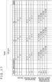
- FIG. 17 is a diagram illustrating an example of the plurality of pieces of predefined setting information (to be selected in step S5 of FIG. 15 ).
- k is an integer equal to or greater than 2.
- the index is an identifier of the setting information
- "P,” "T,” “R1,” and “R2" in the time slots correspond to the position detection, the inclination and azimuth detection, step R1 of the rotation angle detection, and step R2 of the rotation angle detection illustrated in FIG. 5 , respectively.
- an example of the setting information transmitted to the active pen 2C will be illustrated to describe specific content of the setting information.
- the setting information transmitted to the active pen 2C is information including signal content designation information which specifies a first time slot set indicating one or more time slots to be allocated to the pen tip electrode 21, a second time slot set indicating one or more time slots to be allocated to the peripheral electrode 22b, and a third time slot set indicating one or more time slots to be allocated to the peripheral electrode 22c and designates the content of the signal to be transmitted by the active pen 2C from each of the pen tip electrode 21 and the peripheral electrodes 22b and 22c in each time slot.
- the setting information of an index n (0 ⁇ n ⁇ k) specifies time slots such as S n , S k+n , and S 2k+n as the first to third time slot sets.
- all of the specified time slots are used for the position detection (P)
- the signal content designation information included in the setting information is information which designates the normal-phase signal of the in-slot signal as a signal to be transmitted from the pen tip electrode 21 and designates the reverse-phase signal of the in-slot signal as a signal to be transmitted from each of the peripheral electrodes 22b and 22c regarding all of the specified time slots as can be understood from FIG. 5 .
- the active pen 2C transmits the normal-phase signal of the in-slot signal from the pen tip electrode 21 and transmits the reverse-phase signal of the in-slot signal from each of the peripheral electrodes 22b and 22c in each of the specified time slots, and the sensor controller 31 can accurately detect the position (x, y) of the active pen 2C in each time slot.
- the setting information of an index k+n (0 ⁇ n ⁇ k) specifies time slots such as S n , S n+1 , S k+n , S k+n+1 , S 2k+n , and S 2k+n+1 as the first to third time slot sets.
- the signal content designation information included in the setting information is information which designates the normal-phase signal of the in-slot signal as a signal to be transmitted from the pen tip electrode 21 and the reverse-phase signal of the in-slot signal as a signal to be transmitted from each of the peripheral electrodes 22b and 22c regarding the time slots such as S n , S k+n , and S 2k+n used for the position detection (P) and designates the normal-phase signal of the in-slot signal as a signal to be transmitted from each of the pen tip electrode 21 and the peripheral electrodes 22b and 22c regarding the time slots such as S n+1 , S k+n+1 , and S 2k+n+1 used for the inclination and azimuth detection (T).
- the active pen 2C transmits the normal-phase signal of the in-slot signal from the pen tip electrode 21 and transmits the reverse-phase signal of the in-slot signal from each of the peripheral electrodes 22b and 22c in the time slots such as S n , S k+n , and S 2k+n , and the sensor controller 31 can accurately detect the position (x, y) of the active pen 2C in each of the time slots.
- the active pen 2C transmits the normal-phase signal of the in-slot signal from each of the pen tip electrode 21 and the peripheral electrodes 22b and 22c in the time slots such as S n+1 , S k+n+1 , and S 2k+n+1 , and the sensor controller 31 can detect the inclination ⁇ and the azimuth ⁇ of the active pen 2C in each of the time slots.
- the setting information of an index 2k+n (0 ⁇ n ⁇ k) specifies time slots such as S n , S n+1 , S n+2 , S n+3 , S k+n , S k+n+1 , S k+n+2 , S k+n+3 , S 2k+n , S 2k+n+1 , S 2k+n+2 , and S 2k+n+3 as the first to third time slot sets.
- the signal content designation information included in the setting information is information which designates the normal-phase signal of the in-slot signal as a signal to be transmitted from the pen tip electrode 21 and the reverse-phase signal of the in-slot signal as a signal to be transmitted from each of the peripheral electrodes 22b and 22c regarding the time slots such as S n , S k+n , and S 2k+n used for the position detection (P), designates the normal-phase signal of the in-slot signal as a signal to be transmitted from each of the pen tip electrode 21 and the peripheral electrodes 22b and 22c regarding the time slots such as S n+1 , S k+n+1 , and S 2k+n+1 used for the inclination and azimuth detection (T), designates the normal-phase signal of the in-slot signal as a signal to be transmitted from each of the pen tip electrode 21 and the peripheral electrode 22b and the reverse-phase signal of the in-slot signal as a signal to be transmitted from the peripheral electrode 22c regarding the time slots such as S n
- the active pen 2C transmits the normal-phase signal of the in-slot signal from the pen tip electrode 21 and transmits the reverse-phase signal of the in-slot signal from each of the peripheral electrodes 22b and 22c in the time slots such as S n , S k+n , and S 2k+n , and the sensor controller 31 can accurately detect the position (x, y) of the active pen 2C in each of the time slots.
- the active pen 2C transmits the normal-phase signal of the in-slot signal from each of the pen tip electrode 21 and the peripheral electrodes 22b and 22c in the time slots such as S n+1 , S k+n+1 , and S 2k+n+1 , and the sensor controller 31 can detect the inclination ⁇ and the azimuth ⁇ of the active pen 2C in each of the time slots. Furthermore, the active pen 2C transmits the normal-phase signal of the in-slot signal from each of the pen tip electrode 21 and the peripheral electrode 22b and transmits the reverse-phase signal of the in-slot signal from the peripheral electrode 22c in the time slots such as S n+2 , S k+n+2 , and S 2k+n+2 .
- the active pen 2C transmits the normal-phase signal of the in-slot signal from each of the pen tip electrode 21 and the peripheral electrode 22c and transmits the reverse-phase signal of the in-slot signal from the peripheral electrode 22b in the following time slots such as S n+3 , S k+n+3 , and S 2k+n+3 . Therefore, the sensor controller 31 can calculate the rotation angle ⁇ of the active pen 2C after the end of each of the time slots such as S n+3 , S k+n+3 , and S 2k+n+3 .
- the active pen 2A does not correspond to the detection of the inclination and the azimuth and the detection of the rotation angle, and it is preferable that the setting information to be selected by the sensor controller 31 include only the setting information corresponding to the index n (0 ⁇ n ⁇ k) in the setting information illustrated in FIG. 17 .
- the active pen 2B does not correspond to the detection of the rotation angle, and it is preferable that the setting information to be selected by the sensor controller 31 include only the setting information corresponding to the index n (0 ⁇ n ⁇ k) and the index k+n (0 ⁇ n ⁇ k) in the setting information illustrated in FIG. 17 . In this way, the setting information adapted to the functional information of each of the active pens 2A and 2B can be transmitted.
- the sensor controller 31 when the sensor controller 31 is detecting a plurality of active pens 2, it is preferable that the sensor controller 31 selects the setting information without overlapping in electrodes to prevent the active pens 2 from trying to transmit the signals in the same time slot. For example, when the sensor controller 31 is detecting one active pen 2A and one active pen 2C, the sensor controller 31 can, for example, transmit the setting information corresponding to the index 0 to the active pen 2A and transmit the setting information corresponding to the index 2k+1 to the active pen 2C.
- the sensor controller 31 when, for example, the sensor controller 31 is detecting one active pen 2B and one active pen 2C, the sensor controller 31 can, for example, transmit the setting information corresponding to the index k to the active pen 2B and transmit the setting information corresponding to the index 2k+2 to the active pen 2C. In this way, one or more time slots can be allocated to each of the plurality of detected active pens 2 without overlapping in electrodes to thereby favorably calculate the position (x, y), the inclination ⁇ , the azimuth ⁇ , and the rotation angle ⁇ of each active pen 2.
- the sensor controller 31 can designate the time slots on the basis of electrodes according to the number of electrodes of each of one or more detected active pens 2. Therefore, the time slots can be provided in a timely manner according to the functions of each active pen 2. Furthermore, as a result, the position (x, y), the inclination ⁇ , the azimuth ⁇ , and the rotation angle ⁇ of the active pen 2 can be calculated according to the number of electrodes of the active pen 2.
- the transmission rate of the in-slot signal varies among the setting information of the index n (0 ⁇ n ⁇ k) corresponding to only the detection of the position, the setting information of the index k+n (0 ⁇ n ⁇ k) corresponding to the detection of the position, the inclination, and the azimuth, and the setting information of the index 2k+n (0 ⁇ n ⁇ k) corresponding to the detection of the position, the inclination, the azimuth, and the rotation angle in the example of FIG. 17 , the content of the setting information can also be defined to set the transmission rates to a certain value.
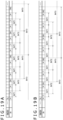
- FIG. 18 is a diagram illustrating a first modification of the plurality of pieces of predefined setting information.
- the setting information of the index n (0 ⁇ n ⁇ k) is the same as the setting information illustrated in FIG. 17 .
- the transmission rate of the active pen 2 based on the setting information is a rate of transmitting once every k time slots.
- the setting information of the index k+n (0 ⁇ n ⁇ k) indicates that the time slots such as S n and S 2k+n are used for the position detection (P), and the time slots such as S k+n and S 3k+n are used for the inclination and azimuth detection (T). Therefore, the transmission rate of the active pen 2 based on the setting information is a rate of transmitting once every k time slots as in the case of the index n (0 ⁇ n ⁇ k).
- the setting information of the index 2k+n (0 ⁇ n ⁇ k) indicates that the time slots such as S n and S 4k+n are used for the position detection (P), the time slots such as S k+n and S 5k+n are used for the inclination and azimuth detection (T), the time slots such as S 2k+n and S 6k+n are used for step R1 of the rotation angle detection, and the time slots such as S 3k+n and S 7k+n are used for step R2 of the rotation angle detection. Therefore, the transmission rate of the active pen 2 based on the setting information is a rate of transmitting once every k time slots as in the case of the index n (0 ⁇ n ⁇ k).
- the content of the setting information can be defined to set, to a certain value, the transmission rate of the active pen 2 based on the setting information.
- the position detection, the inclination and azimuth detection, and the rotation angle detection are performed at the same frequency according to the example of FIG. 17 , the detections may be executed at different frequencies.
- FIG. 19A is a diagram illustrating a second modification of the predefined setting information. Although only the setting information of the index 2k is illustrated in FIG. 19A due to space limitations, this is similar in the setting information of the other indices.
- the setting information illustrated in FIG. 19A indicates that the time slots such as S k , S k+4 , S k+8 , S k+12 , S k+16 , S k+20 , S k+24 , and S k+28 are used for the position detection (P), the time slots such as S k+2 , S k+10 , S k+18 , and S k+26 are used for the inclination and azimuth detection (T), the time slots such as S k+6 and S k+22 are used for step R1 of the rotation angle detection, and the time slots such as S k+14 and S k+30 are used for step R2 of the rotation angle detection. Therefore, execution frequencies of the position detection, the inclination and azimuth detection, and the rotation angle detection can be expressed by a ratio of 4:2:1.
- the content of the setting information can be defined so that the position detection, the inclination and azimuth detection, and the rotation angle detection are executed at different frequencies.
- the position detection, the inclination and azimuth detection, step R1 of the rotation angle detection, and step R2 of the rotation angle detection are executed at certain time intervals. Specifically, the position detection is executed every time INT1 equivalent to time of four time slots, the inclination and azimuth detection is executed every time INT2 equivalent to time of eight time slots, and steps R1 and R2 of the rotation angle detection are executed every time INT3 equivalent to time of sixteen time slots.
- This can increase the accuracy of the ink data generated by the host processor 32 (see FIG. 1 ) according to the results of the position detection, the inclination and azimuth detection, and the rotation angle detection.
- FIG. 19B is a diagram illustrating a modification of the second modification illustrated in FIG. 19A .
- each of the inclination and azimuth detection, step R1 of the rotation angle detection, and step R2 of the rotation angle detection is executed in a time slot that is one time slot before the modification in FIG. 19A .
- This can also define the setting information to execute the position detection, the inclination and azimuth detection, and the rotation angle detection at different frequencies, and in addition, the position detection, the inclination and azimuth detection, step R1 of the rotation angle detection, and step R2 of the rotation angle detection can be executed at certain time intervals.
- the sensor controller 31 determines the setting information for each of the active pens 2 in the example described in FIG. 17 , one piece of setting information may be determined in advance, and a plurality of active pens 2 may be applied to the setting information.
- FIG. 20 is a diagram illustrating a third modification of the predefined setting information.
- An index Z illustrated in FIG. 20 is an example of the setting information corresponding to a plurality of active pens 2.
- time slots such as S 0 , S k , and S 2k are allocated to a first active pen 2
- time slots such as S 1 , S k+1 , and S 2k+1 are allocated to a second active pen 2
- time slots such as S 2 , S k+2 , and S 2k+2 are allocated to a third active pen 2.
- the content of the signal transmitted by each active pen 2 in each time slot may be determined according to the functional information of each active pen 2.
- FIG. 20 illustrates an example in which the first active pen 2 is the active pen 2A, the second active pen 2 is the active pen 2B, and the third active pen 2 is the active pen 2C.
- the signal for the position detection that is, normal-phase signal of in-slot signal transmitted from pen tip electrode 21
- the signals for the position detection that is, normal-phase signal of in-slot signal transmitted from pen tip electrode 21 and reverse-phase signal of in-slot signal transmitted from peripheral electrode 22a
- the signals for the inclination and azimuth detection that is, normal-phase signals of in-slot signals transmitted from pen tip electrode 21 and peripheral electrode 22a
- the signals for the position detection that is, normal-phase signal of in-slot signal transmitted from pen tip electrode 21 and reverse-phase signals of in-slot signals transmitted from peripheral electrodes 22b and 22c
- the signals for the inclination and azimuth detection that is, normal-phase signals of in-slot signals transmitted from pen tip electrode 21 and peripheral electrodes 22b and 22c
- the signals for step R1 of the rotation angle detection that is, normal-phase signals of in-slot signals transmitted from pen tip electrode 21 and peripheral electrode 22b and reverse-phase signal of in-slot signal transmitted from peripheral electrode 22c
- the signals for step R2 of the rotation angle detection that is, normal-phase signals of in-slot signals transmitted from pen tip electrode 21 and peripheral electrode 22c and reverse-phase signal of in-slot signal transmitted from peripheral electrode 22b
- the signals for step R2 of the rotation angle detection that is, normal-phase signals of in-slot signals transmitted from pen tip electrode 21 and peripheral electrode 22c and reverse-phase signal of in-slot signal transmitted from peripheral electrode 22b
- Such a transmission method according to the functional information can be predefined, and the sensor controller 31 can perform the detection operation according to the content of the signal transmitted by the active pen 2. Therefore, the position detection, the inclination and azimuth detection, and the rotation angle detection of each active pen 2 can be favorably executed.
- each of the active pens 2 transmits the downlink signals DS on the basis of the time slots in the example of the system described in the embodiment
- the present disclosure can also be applied to a system that does not use the time slots.
- information designating only the active pen 2 and the content of the signal to be transmitted by the active pen 2 may be arranged in the beacon signal BS, and the designated active pen 2 may transmit the signal including the designated content at arbitrary timing.
- each of the active pens 2 can respond to a predetermined trigger provided from a built-in timer (not illustrated) to transmit the signals from the electrodes in an order determined in advance between the active pen 2 and the sensor controller 31
- the functional information may include information indicating the positional relationship between the pen tip electrode and the peripheral electrode, information indicating the angle of the peripheral electrode with respect to the pen axis, and the like in addition to the number, the shape, and the arrangement of the electrodes provided in the active pen 2C.
- the sensor controller 31 can calculate the inclination, the azimuth, and the rotation angle based on also the information to more accurately obtain the inclination, the azimuth, and the rotation angle of the active pen 2.
- the functional information may include an electrode characteristic profile identifier for specifying one of a plurality of electrode characteristic profiles predefined in relation to the peripheral electrode.
- the sensor controller 31 may determine the type of detection operation (at least any one of position detection, inclination and azimuth detection, and rotation angle detection) to be performed for the active pen 2 based on the electrode characteristic profile identifier.
- the plurality of electrode characteristic profiles may include, for example, an electrode characteristic profile indicating that the peripheral electrode is isotropic with respect to the rotation about the pen axis and an electrode characteristic profile indicating that the peripheral electrode is anisotropic with respect to the rotation about the pen axis.
- the functional information can specify the information described above, and the functional information may be information, such as what is called a pen ID or a pen type ID.
- the setting information may be segmented and transmitted in a plurality of beacon signals BS.
- a first part for specifying the first time slot set in the setting information and a second part for specifying the second time slot set in the setting information may be included and transmitted in different beacon signals BS.
- the first part may include information for designating the length of time of the signals transmitted by using the first time slot set
- the second part may include information for designating the length of time of the signals transmitted by using the second time slot set.
- the active pen 2 may transmit a response signal through the pen tip electrode 21 or the peripheral electrode when the active pen 2 receives the beacon signal BS including the second part.
- the setting information may include information for specifying the type of detection operation corresponding to the sensor controller 31 (for example, information indicating whether or not sensor controller 31 corresponds to inclination detection using peripheral electrode). In this way, the type of signal to be transmitted can be selected on the side of the active pen 2.
- time slot is allocated to each electrode of each active pen 2 in the description of the embodiment
- a unit of communication expressed by a combination of one of a frequency and a code and the time slot may be allocated when the signals transmitted or received in the same time slot can be distinguished by changing the frequency or changing the code. In this case, there may be a case in which the same time slot is allocated to different electrodes.
- the active pen 2C including two peripheral electrodes 22b and 22c obtained by segmenting the peripheral electrode 22a into two parts at a plane including the pen axis is described as an example of the active pen 2 corresponding to the detection of the rotation angle in the embodiment, any active pen 2 including peripheral electrodes in anisotropic shapes with respect to the rotation about the pen axis can detect the rotation angle.
- FIG. 21 is a diagram illustrating peripheral electrodes 22d to 22f included in the active pen 2 according to a modification of the embodiment of the present invention.
- the active pen 2 according to the present modification includes three peripheral electrodes 22d to 22f obtained by dividing the peripheral electrode 22a of the active pen 2B into three equal parts as illustrated in FIG. 21 .
- the peripheral electrodes 22d to 22f also have anisotropic shapes with respect to the rotation about the pen axis, and the active pen 2 according to the present modification can detect the rotation angle.
- FIGS. 21A to 21C illustrate an example of signals transmitted from each of the peripheral electrodes 22d to 22f when the active pen 2 according to the present modification is used to detect the rotation angle.
- the meaning of "+,” “-,” and parentheses in FIGS. 21A to 21C are the same as the meaning in FIG. 5 .
- a step of transmitting the normal-phase signal of the downlink signal DS from the peripheral electrode 22d and transmitting the reverse-phase signals of the downlink signal DS from the peripheral electrodes 22e and 22f ( FIG. 21A ), a step of transmitting the normal-phase signal of the downlink signal DS from the peripheral electrode 22e and transmitting the reverse-phase signals of the downlink signal DS from the peripheral electrodes 22d and 22f ( FIG. 21B ), and a step of transmitting the normal-phase signal of the downlink signal DS from the peripheral electrode 22f and transmitting the reverse-phase signals of the downlink signal DS from the peripheral electrodes 22d and 22e ( FIG. 21C ) can be executed to obtain three positions corresponding to the peripheral electrodes 22d to 22f on the XY plane.
- the sensor controller 31 can calculate the rotation angle of the triangle indicated by the three positions to detect the rotation angle ⁇ of the active pen 2.
- a signal may not be transmitted in the active pen 2 according to the present embodiment, instead of transmitting the reverse-phase signal from each peripheral electrode.
- only one of the two peripheral electrodes that transmit the reverse-phase signals in each of FIGS. 21A to 21C may be configured not to transmit a signal.
- the peripheral electrode 22e may not transmit a signal in FIG. 21A
- the peripheral electrode 22d may not transmit a signal in FIG. 21B
- the peripheral electrode 22f may not transmit a signal in FIG. 21C .
- three positions can also be similarly used to calculate the rotation angle ⁇ of the active pen 2.
Landscapes
- Engineering & Computer Science (AREA)
- General Engineering & Computer Science (AREA)
- Theoretical Computer Science (AREA)
- Human Computer Interaction (AREA)
- Physics & Mathematics (AREA)
- General Physics & Mathematics (AREA)
- Position Input By Displaying (AREA)
- User Interface Of Digital Computer (AREA)
Claims (6)
- Aktiver Stift (2C), der dazu eingerichtet ist, durch kapazitive Kopplung ein Signal an eine Sensorelektrodengruppe (30) zu übertragen, die mit einer Sensorsteuervorrichtung (31) verbunden ist, wobei der aktive Stift (2C) aufweist:eine Stiftspitzenelektrode (21), die in einer Stiftachsenrichtung des aktiven Stifts (2C) an einem vorderen Ende bereitgestellt ist;eine periphere Elektrode, die bei Betrachtung von der Stiftspitzenelektrode (21) her in der Stiftachsenrichtung hinten bereitgestellt ist; undeine Signalverarbeitungseinheit (20), die dazu eingerichtet ist, über die Stiftspitzenelektrode (21) ein Downlinksignal zu übertragen, und die dazu eingerichtet ist, zur gleichen Zeit von der peripheren Elektrode ein Signal mit umgekehrter Phase des Downlinksignals zu übertragen,dadurch gekennzeichnet, dass:um der Sensorsteuervorrichtung (31) zu ermöglichen, einen Rotationswinkel des aktiven Stifts (2C) um die Stiftachse zu erkennen, die periphere Elektrode mehrere segmentierte Elektroden (22b, 22c) mit in Bezug auf eine Rotation um die Stiftachse anisotropischen Formen aufweist, unddie Signalverarbeitungseinheit (20) dazu eingerichtet ist, jede der mehreren segmentierten Elektroden (22b, 22c) einzeln zu schalten, um das Downlinksignal zu übertragen oder das Signal mit umgekehrter Phase zu übertragen.
- Aktiver Stift (2C) nach Anspruch 1, wobei
die Signalverarbeitungseinheit (20) dazu eingerichtet ist, das Übertragen des Signals mit umgekehrter Phase von der peripheren Elektrode gemäß einem vordefinierten Auslöser zu beenden. - Aktiver Stift (2C) nach Anspruch 1, wobei
die Signalverarbeitungseinheit (20) dazu eingerichtet ist, das Übertragen des Downlinksignals von der Stiftspitzenelektrode (21) gemäß einem vordefinierten Auslöser zu starten. - Aktiver Stift (2C) nach Anspruch 1, wobei
die Signalverarbeitungseinheit (20) dazu eingerichtet ist, ein vorbestimmtes Kommunikationsverfahren zu benutzen, um die Sensorsteuervorrichtung (31) darüber zu benachrichtigen, dass die periphere Elektrode die mehreren segmentierten Elektroden (22b, 22c) aufweist. - Aktiver Stift (2C) nach Anspruch 2 oder 3, wobei
der vorbestimmte Auslöser von einem in den aktiven Stift (2C) eingebauten Zeitgeber bereitgestellt wird. - Aktiver Stift (2C) nach Anspruch 2 oder 3, wobei
der vorbestimmte Auslöser von einem Bakensignal bereitgestellt wird, das von der Sensorsteuervorrichtung (31) übertragen wird.
Priority Applications (1)
| Application Number | Priority Date | Filing Date | Title |
|---|---|---|---|
| EP22178635.3A EP4080333B1 (de) | 2017-11-29 | 2017-11-29 | Aktiver stift |
Applications Claiming Priority (3)
| Application Number | Priority Date | Filing Date | Title |
|---|---|---|---|
| PCT/JP2017/042777 WO2019106747A1 (ja) | 2017-11-29 | 2017-11-29 | アクティブペンとセンサコントローラとの間で実行される通信方法及びアクティブペン |
| EP22178635.3A EP4080333B1 (de) | 2017-11-29 | 2017-11-29 | Aktiver stift |
| EP17933372.9A EP3719620B1 (de) | 2017-11-29 | 2017-11-29 | Kommunikationsverfahren, das zwischen einem aktiven stift und einer sensorsteuerung ausgeführt wird |
Related Parent Applications (2)
| Application Number | Title | Priority Date | Filing Date |
|---|---|---|---|
| EP17933372.9A Division EP3719620B1 (de) | 2017-11-29 | 2017-11-29 | Kommunikationsverfahren, das zwischen einem aktiven stift und einer sensorsteuerung ausgeführt wird |
| EP17933372.9A Division-Into EP3719620B1 (de) | 2017-11-29 | 2017-11-29 | Kommunikationsverfahren, das zwischen einem aktiven stift und einer sensorsteuerung ausgeführt wird |
Publications (2)
| Publication Number | Publication Date |
|---|---|
| EP4080333A1 EP4080333A1 (de) | 2022-10-26 |
| EP4080333B1 true EP4080333B1 (de) | 2024-07-17 |
Family
ID=66665600
Family Applications (2)
| Application Number | Title | Priority Date | Filing Date |
|---|---|---|---|
| EP17933372.9A Active EP3719620B1 (de) | 2017-11-29 | 2017-11-29 | Kommunikationsverfahren, das zwischen einem aktiven stift und einer sensorsteuerung ausgeführt wird |
| EP22178635.3A Active EP4080333B1 (de) | 2017-11-29 | 2017-11-29 | Aktiver stift |
Family Applications Before (1)
| Application Number | Title | Priority Date | Filing Date |
|---|---|---|---|
| EP17933372.9A Active EP3719620B1 (de) | 2017-11-29 | 2017-11-29 | Kommunikationsverfahren, das zwischen einem aktiven stift und einer sensorsteuerung ausgeführt wird |
Country Status (5)
| Country | Link |
|---|---|
| US (5) | US11360586B2 (de) |
| EP (2) | EP3719620B1 (de) |
| JP (2) | JP6920007B2 (de) |
| CN (1) | CN111373357B (de) |
| WO (1) | WO2019106747A1 (de) |
Families Citing this family (11)
| Publication number | Priority date | Publication date | Assignee | Title |
|---|---|---|---|---|
| JP5442479B2 (ja) * | 2010-02-05 | 2014-03-12 | 株式会社ワコム | 指示体、位置検出装置及び位置検出方法 |
| JP5669263B2 (ja) * | 2011-04-11 | 2015-02-12 | 株式会社ワコム | 位置指示器 |
| JP5745712B1 (ja) | 2014-01-22 | 2015-07-08 | 株式会社ワコム | 位置指示器、位置検出装置、位置検出回路及び位置検出方法 |
| JP6908442B2 (ja) * | 2017-06-06 | 2021-07-28 | 株式会社ワコム | 位置指示器 |
| CN111373357B (zh) | 2017-11-29 | 2023-09-22 | 株式会社和冠 | 在主动笔与传感器控制器之间执行的通信方法及主动笔 |
| JP7323336B2 (ja) * | 2019-05-24 | 2023-08-08 | 株式会社ワコム | 位置指示器及び座標入力装置 |
| JP7346160B2 (ja) * | 2019-08-23 | 2023-09-19 | 株式会社ワコム | スタイラス及び集積回路 |
| CN110968208B (zh) * | 2019-11-28 | 2023-06-23 | 京东方科技集团股份有限公司 | 触控笔、触控笔检测方法和触控系统 |
| JP7562231B2 (ja) * | 2020-09-07 | 2024-10-07 | 株式会社ワコム | パームリジェクションの方法及びセンサコントローラ |
| WO2025005103A1 (ja) * | 2023-06-27 | 2025-01-02 | 株式会社ワコム | センサおよび位置検出装置 |
| TWI871089B (zh) * | 2023-11-14 | 2025-01-21 | 禾瑞亞科技股份有限公司 | 主動觸控筆與其處理電路和處理方法、觸控處理裝置與其觸控處理方法、觸控系統 |
Family Cites Families (26)
| Publication number | Priority date | Publication date | Assignee | Title |
|---|---|---|---|---|
| JPS51107590A (en) | 1975-03-19 | 1976-09-24 | Tokyo Shibaura Electric Co | Uzumakitetsushinno kakohoho |
| JPS606191A (ja) | 1983-06-02 | 1985-01-12 | Wakamoto Pharmaceut Co Ltd | 低分子ウロキナ−ゼと高分子ウロキナ−ゼの分離方法 |
| JP5442479B2 (ja) | 2010-02-05 | 2014-03-12 | 株式会社ワコム | 指示体、位置検出装置及び位置検出方法 |
| US8638320B2 (en) * | 2011-06-22 | 2014-01-28 | Apple Inc. | Stylus orientation detection |
| CN202815747U (zh) * | 2012-08-31 | 2013-03-20 | 深圳市汇顶科技有限公司 | 电容屏触摸笔 |
| CN108549494B (zh) * | 2013-11-08 | 2021-01-01 | 禾瑞亚科技股份有限公司 | 发信器 |
| US9606680B1 (en) * | 2014-06-12 | 2017-03-28 | Amazon Technologies, Inc. | Capacitive communication between stylus devices and computing devices |
| CN106462306B (zh) * | 2014-06-27 | 2020-09-29 | 3M创新有限公司 | 触摸系统触笔和方法 |
| JP6487694B2 (ja) | 2014-12-26 | 2019-03-20 | 株式会社ワコム | 位置指示器及び信号処理装置 |
| KR102389701B1 (ko) * | 2015-01-19 | 2022-04-22 | 가부시키가이샤 와코무 | 위치 지시기 |
| JPWO2016121045A1 (ja) * | 2015-01-29 | 2017-11-09 | 株式会社ワコム | 静電ペン |
| JP6544791B2 (ja) | 2015-02-20 | 2019-07-17 | 株式会社ワコム | 位置指示器、信号処理回路、信号供給制御方法及び信号処理方法 |
| US9977519B2 (en) | 2015-02-25 | 2018-05-22 | Synaptics Incorporated | Active pen with bidirectional communication |
| CN113238669B (zh) | 2015-04-09 | 2023-08-08 | 株式会社和冠 | 主动式触控笔 |
| CN107533385B (zh) * | 2015-04-20 | 2022-03-11 | 株式会社和冠 | 使用了主动式触控笔及传感器控制器的方法、传感器控制器、主动式触控笔及系统 |
| US9639183B2 (en) | 2015-04-20 | 2017-05-02 | Wacom Co., Ltd. | System and method for bidirectional communication between stylus and stylus sensor controller |
| CN112181175B (zh) | 2015-04-20 | 2024-05-31 | 株式会社和冠 | 传感器控制器、主动式触控笔及使用了它们的方法 |
| US10082890B2 (en) * | 2015-09-01 | 2018-09-25 | Microsoft Technology Licensing, Llc | Electrostatic communication using an active stylus |
| CN112416149B (zh) * | 2016-03-08 | 2024-08-20 | 禾瑞亚科技股份有限公司 | 侦测触控笔的倾斜角的触控控制装置与其控制方法 |
| KR102506658B1 (ko) * | 2016-05-13 | 2023-03-06 | 엘지디스플레이 주식회사 | 터치 스크린 장치 및 그의 구동 방법 |
| TWI597645B (zh) * | 2016-10-05 | 2017-09-01 | 翰碩電子股份有限公司 | 電容筆發射與應用訊號的方法及應用此方法之電容筆 |
| US10474286B2 (en) * | 2016-10-25 | 2019-11-12 | Lg Display Co., Ltd. | Touch display device, active pen, touch system, touch circuit, and pen recognition method |
| TWI571776B (zh) * | 2016-10-28 | 2017-02-21 | 翰碩電子股份有限公司 | 應用同步時間差發射訊號的方法之電容筆與觸控輸入裝置 |
| US10073548B2 (en) * | 2016-11-08 | 2018-09-11 | Wacom Co., Ltd. | Stylus having variable transmit signal strength, and sensor for detecting such stylus |
| US10439753B2 (en) * | 2017-05-25 | 2019-10-08 | Microsoft Technology Licensing, Llc | Multi-protocol communications between host devices and stylus devices |
| CN111373357B (zh) * | 2017-11-29 | 2023-09-22 | 株式会社和冠 | 在主动笔与传感器控制器之间执行的通信方法及主动笔 |
-
2017
- 2017-11-29 CN CN201780096383.9A patent/CN111373357B/zh active Active
- 2017-11-29 WO PCT/JP2017/042777 patent/WO2019106747A1/ja not_active Ceased
- 2017-11-29 EP EP17933372.9A patent/EP3719620B1/de active Active
- 2017-11-29 EP EP22178635.3A patent/EP4080333B1/de active Active
- 2017-11-29 JP JP2019556453A patent/JP6920007B2/ja active Active
-
2020
- 2020-03-31 US US16/836,494 patent/US11360586B2/en active Active
-
2021
- 2021-07-22 JP JP2021121096A patent/JP7098801B2/ja active Active
-
2022
- 2022-04-28 US US17/732,253 patent/US11720189B2/en active Active
-
2023
- 2023-06-21 US US18/339,018 patent/US12079406B2/en active Active
-
2024
- 2024-08-01 US US18/792,227 patent/US12474794B2/en active Active
-
2025
- 2025-10-21 US US19/364,774 patent/US20260044224A1/en active Pending
Also Published As
| Publication number | Publication date |
|---|---|
| JP2021168204A (ja) | 2021-10-21 |
| EP3719620A4 (de) | 2021-03-17 |
| US12079406B2 (en) | 2024-09-03 |
| JPWO2019106747A1 (ja) | 2020-11-19 |
| US20200225773A1 (en) | 2020-07-16 |
| CN111373357A (zh) | 2020-07-03 |
| CN111373357B (zh) | 2023-09-22 |
| US20230350507A1 (en) | 2023-11-02 |
| EP3719620A1 (de) | 2020-10-07 |
| US20240393892A1 (en) | 2024-11-28 |
| US20220253157A1 (en) | 2022-08-11 |
| US11360586B2 (en) | 2022-06-14 |
| WO2019106747A1 (ja) | 2019-06-06 |
| US11720189B2 (en) | 2023-08-08 |
| US12474794B2 (en) | 2025-11-18 |
| EP4080333A1 (de) | 2022-10-26 |
| JP6920007B2 (ja) | 2021-08-18 |
| US20260044224A1 (en) | 2026-02-12 |
| JP7098801B2 (ja) | 2022-07-11 |
| EP3719620B1 (de) | 2022-09-07 |
Similar Documents
| Publication | Publication Date | Title |
|---|---|---|
| EP4080333B1 (de) | Aktiver stift | |
| US20250110585A1 (en) | Active pen and sensor controller that use data generated from identification data | |
| JP7215881B2 (ja) | センサコントローラ | |
| US10429955B2 (en) | Pointer, position detection apparatus and position detection method | |
| US11379059B2 (en) | Stylus, touch panel, display device and touch sensing method | |
| US9977519B2 (en) | Active pen with bidirectional communication | |
| EP3427133B1 (de) | Stift in der feldstärkenmessungskalibrierung | |
| CN107111388A (zh) | 与数字化仪的通用触控笔通信 | |
| GB2466566A (en) | Methods of operation a digitiser with an autonomous asynchronous stylus | |
| JP6914267B2 (ja) | ペアリング方法、位置検出システム、位置指示器、及び位置検出装置 | |
| CN113126810A (zh) | 发信器、触控处理装置与其处理方法和电子系统 | |
| JP2021193625A (ja) | ポインタの位置検出方法 | |
| CN115543105B (zh) | 一种信息传输方法和装置 | |
| CN115480667A (zh) | 用于辅助设备的电容性通信信道 |
Legal Events
| Date | Code | Title | Description |
|---|---|---|---|
| PUAI | Public reference made under article 153(3) epc to a published international application that has entered the european phase |
Free format text: ORIGINAL CODE: 0009012 |
|
| STAA | Information on the status of an ep patent application or granted ep patent |
Free format text: STATUS: THE APPLICATION HAS BEEN PUBLISHED |
|
| AC | Divisional application: reference to earlier application |
Ref document number: 3719620 Country of ref document: EP Kind code of ref document: P |
|
| AK | Designated contracting states |
Kind code of ref document: A1 Designated state(s): AL AT BE BG CH CY CZ DE DK EE ES FI FR GB GR HR HU IE IS IT LI LT LU LV MC MK MT NL NO PL PT RO RS SE SI SK SM TR |
|
| STAA | Information on the status of an ep patent application or granted ep patent |
Free format text: STATUS: REQUEST FOR EXAMINATION WAS MADE |
|
| 17P | Request for examination filed |
Effective date: 20230419 |
|
| RBV | Designated contracting states (corrected) |
Designated state(s): AL AT BE BG CH CY CZ DE DK EE ES FI FR GB GR HR HU IE IS IT LI LT LU LV MC MK MT NL NO PL PT RO RS SE SI SK SM TR |
|
| GRAP | Despatch of communication of intention to grant a patent |
Free format text: ORIGINAL CODE: EPIDOSNIGR1 |
|
| STAA | Information on the status of an ep patent application or granted ep patent |
Free format text: STATUS: GRANT OF PATENT IS INTENDED |
|
| INTG | Intention to grant announced |
Effective date: 20240216 |
|
| GRAS | Grant fee paid |
Free format text: ORIGINAL CODE: EPIDOSNIGR3 |
|
| GRAA | (expected) grant |
Free format text: ORIGINAL CODE: 0009210 |
|
| STAA | Information on the status of an ep patent application or granted ep patent |
Free format text: STATUS: THE PATENT HAS BEEN GRANTED |
|
| AC | Divisional application: reference to earlier application |
Ref document number: 3719620 Country of ref document: EP Kind code of ref document: P |
|
| AK | Designated contracting states |
Kind code of ref document: B1 Designated state(s): AL AT BE BG CH CY CZ DE DK EE ES FI FR GB GR HR HU IE IS IT LI LT LU LV MC MK MT NL NO PL PT RO RS SE SI SK SM TR |
|
| REG | Reference to a national code |
Ref country code: CH Ref legal event code: EP |
|
| REG | Reference to a national code |
Ref country code: DE Ref legal event code: R096 Ref document number: 602017083459 Country of ref document: DE |
|
| REG | Reference to a national code |
Ref country code: IE Ref legal event code: FG4D |
|
| REG | Reference to a national code |
Ref country code: LT Ref legal event code: MG9D |
|
| REG | Reference to a national code |
Ref country code: NL Ref legal event code: MP Effective date: 20240717 |
|
| PG25 | Lapsed in a contracting state [announced via postgrant information from national office to epo] |
Ref country code: PT Free format text: LAPSE BECAUSE OF FAILURE TO SUBMIT A TRANSLATION OF THE DESCRIPTION OR TO PAY THE FEE WITHIN THE PRESCRIBED TIME-LIMIT Effective date: 20241118 |
|
| REG | Reference to a national code |
Ref country code: AT Ref legal event code: MK05 Ref document number: 1704758 Country of ref document: AT Kind code of ref document: T Effective date: 20240717 |
|
| PG25 | Lapsed in a contracting state [announced via postgrant information from national office to epo] |
Ref country code: NL Free format text: LAPSE BECAUSE OF FAILURE TO SUBMIT A TRANSLATION OF THE DESCRIPTION OR TO PAY THE FEE WITHIN THE PRESCRIBED TIME-LIMIT Effective date: 20240717 |
|
| PG25 | Lapsed in a contracting state [announced via postgrant information from national office to epo] |
Ref country code: PT Free format text: LAPSE BECAUSE OF FAILURE TO SUBMIT A TRANSLATION OF THE DESCRIPTION OR TO PAY THE FEE WITHIN THE PRESCRIBED TIME-LIMIT Effective date: 20241118 Ref country code: NL Free format text: LAPSE BECAUSE OF FAILURE TO SUBMIT A TRANSLATION OF THE DESCRIPTION OR TO PAY THE FEE WITHIN THE PRESCRIBED TIME-LIMIT Effective date: 20240717 |
|
| PGFP | Annual fee paid to national office [announced via postgrant information from national office to epo] |
Ref country code: DE Payment date: 20241121 Year of fee payment: 8 |
|
| PG25 | Lapsed in a contracting state [announced via postgrant information from national office to epo] |
Ref country code: NO Free format text: LAPSE BECAUSE OF FAILURE TO SUBMIT A TRANSLATION OF THE DESCRIPTION OR TO PAY THE FEE WITHIN THE PRESCRIBED TIME-LIMIT Effective date: 20241017 |
|
| PG25 | Lapsed in a contracting state [announced via postgrant information from national office to epo] |
Ref country code: FI Free format text: LAPSE BECAUSE OF FAILURE TO SUBMIT A TRANSLATION OF THE DESCRIPTION OR TO PAY THE FEE WITHIN THE PRESCRIBED TIME-LIMIT Effective date: 20240717 Ref country code: PL Free format text: LAPSE BECAUSE OF FAILURE TO SUBMIT A TRANSLATION OF THE DESCRIPTION OR TO PAY THE FEE WITHIN THE PRESCRIBED TIME-LIMIT Effective date: 20240717 Ref country code: GR Free format text: LAPSE BECAUSE OF FAILURE TO SUBMIT A TRANSLATION OF THE DESCRIPTION OR TO PAY THE FEE WITHIN THE PRESCRIBED TIME-LIMIT Effective date: 20241018 |
|
| PGFP | Annual fee paid to national office [announced via postgrant information from national office to epo] |
Ref country code: GB Payment date: 20241120 Year of fee payment: 8 |
|
| PG25 | Lapsed in a contracting state [announced via postgrant information from national office to epo] |
Ref country code: BG Free format text: LAPSE BECAUSE OF FAILURE TO SUBMIT A TRANSLATION OF THE DESCRIPTION OR TO PAY THE FEE WITHIN THE PRESCRIBED TIME-LIMIT Effective date: 20240717 |
|
| PG25 | Lapsed in a contracting state [announced via postgrant information from national office to epo] |
Ref country code: LV Free format text: LAPSE BECAUSE OF FAILURE TO SUBMIT A TRANSLATION OF THE DESCRIPTION OR TO PAY THE FEE WITHIN THE PRESCRIBED TIME-LIMIT Effective date: 20240717 |
|
| PG25 | Lapsed in a contracting state [announced via postgrant information from national office to epo] |
Ref country code: AT Free format text: LAPSE BECAUSE OF FAILURE TO SUBMIT A TRANSLATION OF THE DESCRIPTION OR TO PAY THE FEE WITHIN THE PRESCRIBED TIME-LIMIT Effective date: 20240717 Ref country code: IS Free format text: LAPSE BECAUSE OF FAILURE TO SUBMIT A TRANSLATION OF THE DESCRIPTION OR TO PAY THE FEE WITHIN THE PRESCRIBED TIME-LIMIT Effective date: 20241117 |
|
| PG25 | Lapsed in a contracting state [announced via postgrant information from national office to epo] |
Ref country code: HR Free format text: LAPSE BECAUSE OF FAILURE TO SUBMIT A TRANSLATION OF THE DESCRIPTION OR TO PAY THE FEE WITHIN THE PRESCRIBED TIME-LIMIT Effective date: 20240717 |
|
| PG25 | Lapsed in a contracting state [announced via postgrant information from national office to epo] |
Ref country code: ES Free format text: LAPSE BECAUSE OF FAILURE TO SUBMIT A TRANSLATION OF THE DESCRIPTION OR TO PAY THE FEE WITHIN THE PRESCRIBED TIME-LIMIT Effective date: 20240717 Ref country code: RS Free format text: LAPSE BECAUSE OF FAILURE TO SUBMIT A TRANSLATION OF THE DESCRIPTION OR TO PAY THE FEE WITHIN THE PRESCRIBED TIME-LIMIT Effective date: 20241017 |
|
| PG25 | Lapsed in a contracting state [announced via postgrant information from national office to epo] |
Ref country code: RS Free format text: LAPSE BECAUSE OF FAILURE TO SUBMIT A TRANSLATION OF THE DESCRIPTION OR TO PAY THE FEE WITHIN THE PRESCRIBED TIME-LIMIT Effective date: 20241017 Ref country code: PL Free format text: LAPSE BECAUSE OF FAILURE TO SUBMIT A TRANSLATION OF THE DESCRIPTION OR TO PAY THE FEE WITHIN THE PRESCRIBED TIME-LIMIT Effective date: 20240717 Ref country code: NO Free format text: LAPSE BECAUSE OF FAILURE TO SUBMIT A TRANSLATION OF THE DESCRIPTION OR TO PAY THE FEE WITHIN THE PRESCRIBED TIME-LIMIT Effective date: 20241017 Ref country code: LV Free format text: LAPSE BECAUSE OF FAILURE TO SUBMIT A TRANSLATION OF THE DESCRIPTION OR TO PAY THE FEE WITHIN THE PRESCRIBED TIME-LIMIT Effective date: 20240717 Ref country code: IS Free format text: LAPSE BECAUSE OF FAILURE TO SUBMIT A TRANSLATION OF THE DESCRIPTION OR TO PAY THE FEE WITHIN THE PRESCRIBED TIME-LIMIT Effective date: 20241117 Ref country code: HR Free format text: LAPSE BECAUSE OF FAILURE TO SUBMIT A TRANSLATION OF THE DESCRIPTION OR TO PAY THE FEE WITHIN THE PRESCRIBED TIME-LIMIT Effective date: 20240717 Ref country code: GR Free format text: LAPSE BECAUSE OF FAILURE TO SUBMIT A TRANSLATION OF THE DESCRIPTION OR TO PAY THE FEE WITHIN THE PRESCRIBED TIME-LIMIT Effective date: 20241018 Ref country code: FI Free format text: LAPSE BECAUSE OF FAILURE TO SUBMIT A TRANSLATION OF THE DESCRIPTION OR TO PAY THE FEE WITHIN THE PRESCRIBED TIME-LIMIT Effective date: 20240717 Ref country code: ES Free format text: LAPSE BECAUSE OF FAILURE TO SUBMIT A TRANSLATION OF THE DESCRIPTION OR TO PAY THE FEE WITHIN THE PRESCRIBED TIME-LIMIT Effective date: 20240717 Ref country code: BG Free format text: LAPSE BECAUSE OF FAILURE TO SUBMIT A TRANSLATION OF THE DESCRIPTION OR TO PAY THE FEE WITHIN THE PRESCRIBED TIME-LIMIT Effective date: 20240717 Ref country code: AT Free format text: LAPSE BECAUSE OF FAILURE TO SUBMIT A TRANSLATION OF THE DESCRIPTION OR TO PAY THE FEE WITHIN THE PRESCRIBED TIME-LIMIT Effective date: 20240717 |
|
| PG25 | Lapsed in a contracting state [announced via postgrant information from national office to epo] |
Ref country code: RO Free format text: LAPSE BECAUSE OF FAILURE TO SUBMIT A TRANSLATION OF THE DESCRIPTION OR TO PAY THE FEE WITHIN THE PRESCRIBED TIME-LIMIT Effective date: 20240717 Ref country code: SM Free format text: LAPSE BECAUSE OF FAILURE TO SUBMIT A TRANSLATION OF THE DESCRIPTION OR TO PAY THE FEE WITHIN THE PRESCRIBED TIME-LIMIT Effective date: 20240717 Ref country code: DK Free format text: LAPSE BECAUSE OF FAILURE TO SUBMIT A TRANSLATION OF THE DESCRIPTION OR TO PAY THE FEE WITHIN THE PRESCRIBED TIME-LIMIT Effective date: 20240717 |
|
| REG | Reference to a national code |
Ref country code: DE Ref legal event code: R097 Ref document number: 602017083459 Country of ref document: DE |
|
| PG25 | Lapsed in a contracting state [announced via postgrant information from national office to epo] |
Ref country code: EE Free format text: LAPSE BECAUSE OF FAILURE TO SUBMIT A TRANSLATION OF THE DESCRIPTION OR TO PAY THE FEE WITHIN THE PRESCRIBED TIME-LIMIT Effective date: 20240717 |
|
| PG25 | Lapsed in a contracting state [announced via postgrant information from national office to epo] |
Ref country code: CZ Free format text: LAPSE BECAUSE OF FAILURE TO SUBMIT A TRANSLATION OF THE DESCRIPTION OR TO PAY THE FEE WITHIN THE PRESCRIBED TIME-LIMIT Effective date: 20240717 |
|
| PG25 | Lapsed in a contracting state [announced via postgrant information from national office to epo] |
Ref country code: SK Free format text: LAPSE BECAUSE OF FAILURE TO SUBMIT A TRANSLATION OF THE DESCRIPTION OR TO PAY THE FEE WITHIN THE PRESCRIBED TIME-LIMIT Effective date: 20240717 |
|
| PLBE | No opposition filed within time limit |
Free format text: ORIGINAL CODE: 0009261 |
|
| STAA | Information on the status of an ep patent application or granted ep patent |
Free format text: STATUS: NO OPPOSITION FILED WITHIN TIME LIMIT |
|
| 26N | No opposition filed |
Effective date: 20250422 |
|
| REG | Reference to a national code |
Ref country code: CH Ref legal event code: PL |
|
| PG25 | Lapsed in a contracting state [announced via postgrant information from national office to epo] |
Ref country code: MC Free format text: LAPSE BECAUSE OF FAILURE TO SUBMIT A TRANSLATION OF THE DESCRIPTION OR TO PAY THE FEE WITHIN THE PRESCRIBED TIME-LIMIT Effective date: 20240717 |
|
| PG25 | Lapsed in a contracting state [announced via postgrant information from national office to epo] |
Ref country code: LU Free format text: LAPSE BECAUSE OF NON-PAYMENT OF DUE FEES Effective date: 20241129 |
|
| REG | Reference to a national code |
Ref country code: CH Ref legal event code: PL |
|
| PG25 | Lapsed in a contracting state [announced via postgrant information from national office to epo] |
Ref country code: CH Free format text: LAPSE BECAUSE OF NON-PAYMENT OF DUE FEES Effective date: 20241130 |
|
| REG | Reference to a national code |
Ref country code: BE Ref legal event code: MM Effective date: 20241130 |
|
| PG25 | Lapsed in a contracting state [announced via postgrant information from national office to epo] |
Ref country code: SE Free format text: LAPSE BECAUSE OF FAILURE TO SUBMIT A TRANSLATION OF THE DESCRIPTION OR TO PAY THE FEE WITHIN THE PRESCRIBED TIME-LIMIT Effective date: 20240717 |
|
| PG25 | Lapsed in a contracting state [announced via postgrant information from national office to epo] |
Ref country code: BE Free format text: LAPSE BECAUSE OF NON-PAYMENT OF DUE FEES Effective date: 20241130 |
|
| PG25 | Lapsed in a contracting state [announced via postgrant information from national office to epo] |
Ref country code: FR Free format text: LAPSE BECAUSE OF NON-PAYMENT OF DUE FEES Effective date: 20241130 |
|
| PG25 | Lapsed in a contracting state [announced via postgrant information from national office to epo] |
Ref country code: IE Free format text: LAPSE BECAUSE OF NON-PAYMENT OF DUE FEES Effective date: 20241129 |
|
| PG25 | Lapsed in a contracting state [announced via postgrant information from national office to epo] |
Ref country code: IT Free format text: LAPSE BECAUSE OF FAILURE TO SUBMIT A TRANSLATION OF THE DESCRIPTION OR TO PAY THE FEE WITHIN THE PRESCRIBED TIME-LIMIT Effective date: 20240717 |
|
| PG25 | Lapsed in a contracting state [announced via postgrant information from national office to epo] |
Ref country code: HU Free format text: LAPSE BECAUSE OF FAILURE TO SUBMIT A TRANSLATION OF THE DESCRIPTION OR TO PAY THE FEE WITHIN THE PRESCRIBED TIME-LIMIT; INVALID AB INITIO Effective date: 20171129 |
|
| PG25 | Lapsed in a contracting state [announced via postgrant information from national office to epo] |
Ref country code: CY Free format text: LAPSE BECAUSE OF FAILURE TO SUBMIT A TRANSLATION OF THE DESCRIPTION OR TO PAY THE FEE WITHIN THE PRESCRIBED TIME-LIMIT; INVALID AB INITIO Effective date: 20171129 |