EP4079678A1 - Mems rotor with coated bottom surface - Google Patents
Mems rotor with coated bottom surface Download PDFInfo
- Publication number
- EP4079678A1 EP4079678A1 EP22158410.5A EP22158410A EP4079678A1 EP 4079678 A1 EP4079678 A1 EP 4079678A1 EP 22158410 A EP22158410 A EP 22158410A EP 4079678 A1 EP4079678 A1 EP 4079678A1
- Authority
- EP
- European Patent Office
- Prior art keywords
- coating layer
- rotor
- top surface
- device wafer
- density
- Prior art date
- Legal status (The legal status is an assumption and is not a legal conclusion. Google has not performed a legal analysis and makes no representation as to the accuracy of the status listed.)
- Pending
Links
Images

Classifications
-
- B—PERFORMING OPERATIONS; TRANSPORTING
- B81—MICROSTRUCTURAL TECHNOLOGY
- B81B—MICROSTRUCTURAL DEVICES OR SYSTEMS, e.g. MICROMECHANICAL DEVICES
- B81B3/00—Devices comprising flexible or deformable elements, e.g. comprising elastic tongues or membranes
- B81B3/0035—Constitution or structural means for controlling the movement of the flexible or deformable elements
- B81B3/004—Angular deflection
- B81B3/0045—Improve properties related to angular swinging, e.g. control resonance frequency
-
- B—PERFORMING OPERATIONS; TRANSPORTING
- B81—MICROSTRUCTURAL TECHNOLOGY
- B81B—MICROSTRUCTURAL DEVICES OR SYSTEMS, e.g. MICROMECHANICAL DEVICES
- B81B5/00—Devices comprising elements which are movable in relation to each other, e.g. comprising slidable or rotatable elements
-
- B—PERFORMING OPERATIONS; TRANSPORTING
- B81—MICROSTRUCTURAL TECHNOLOGY
- B81C—PROCESSES OR APPARATUS SPECIALLY ADAPTED FOR THE MANUFACTURE OR TREATMENT OF MICROSTRUCTURAL DEVICES OR SYSTEMS
- B81C1/00—Manufacture or treatment of devices or systems in or on a substrate
- B81C1/00015—Manufacture or treatment of devices or systems in or on a substrate for manufacturing microsystems
- B81C1/00198—Manufacture or treatment of devices or systems in or on a substrate for manufacturing microsystems comprising elements which are movable in relation to each other, e.g. comprising slidable or rotatable elements
-
- B—PERFORMING OPERATIONS; TRANSPORTING
- B81—MICROSTRUCTURAL TECHNOLOGY
- B81B—MICROSTRUCTURAL DEVICES OR SYSTEMS, e.g. MICROMECHANICAL DEVICES
- B81B2201/00—Specific applications of microelectromechanical systems
- B81B2201/02—Sensors
- B81B2201/0228—Inertial sensors
- B81B2201/0235—Accelerometers
-
- B—PERFORMING OPERATIONS; TRANSPORTING
- B81—MICROSTRUCTURAL TECHNOLOGY
- B81B—MICROSTRUCTURAL DEVICES OR SYSTEMS, e.g. MICROMECHANICAL DEVICES
- B81B2201/00—Specific applications of microelectromechanical systems
- B81B2201/02—Sensors
- B81B2201/0228—Inertial sensors
- B81B2201/0242—Gyroscopes
-
- B—PERFORMING OPERATIONS; TRANSPORTING
- B81—MICROSTRUCTURAL TECHNOLOGY
- B81B—MICROSTRUCTURAL DEVICES OR SYSTEMS, e.g. MICROMECHANICAL DEVICES
- B81B2203/00—Basic microelectromechanical structures
- B81B2203/03—Static structures
- B81B2203/0315—Cavities
-
- B—PERFORMING OPERATIONS; TRANSPORTING
- B81—MICROSTRUCTURAL TECHNOLOGY
- B81B—MICROSTRUCTURAL DEVICES OR SYSTEMS, e.g. MICROMECHANICAL DEVICES
- B81B2203/00—Basic microelectromechanical structures
- B81B2203/05—Type of movement
- B81B2203/058—Rotation out of a plane parallel to the substrate
-
- B—PERFORMING OPERATIONS; TRANSPORTING
- B81—MICROSTRUCTURAL TECHNOLOGY
- B81B—MICROSTRUCTURAL DEVICES OR SYSTEMS, e.g. MICROMECHANICAL DEVICES
- B81B2203/00—Basic microelectromechanical structures
- B81B2203/06—Devices comprising elements which are movable in relation to each other, e.g. slidable or rotatable
-
- B—PERFORMING OPERATIONS; TRANSPORTING
- B81—MICROSTRUCTURAL TECHNOLOGY
- B81C—PROCESSES OR APPARATUS SPECIALLY ADAPTED FOR THE MANUFACTURE OR TREATMENT OF MICROSTRUCTURAL DEVICES OR SYSTEMS
- B81C2203/00—Forming microstructural systems
- B81C2203/03—Bonding two components
- B81C2203/033—Thermal bonding
- B81C2203/036—Fusion bonding
Definitions
- This disclosure relates to micromechanical devices, and particularly to micromechanical devices formed in a device wafer which is bonded to a handle wafer.
- the present disclosure further concerns the mass of a mobile rotor formed in the device wafer.
- Microelectromechanical (MEMS) devices are typically manufactured from silicon substrates.
- the micromechanical structures may be formed in a device wafer which has been bonded to a thicker handle wafer for structural support.
- the micromechanical structures often include a rotor which is mobile in relation to the fixed parts of the device wafer.
- a cavity can be formed in the region of the handle wafer which will lie beneath the rotor.
- microelectromechanical structures in the device wafer usually requires gaps which are etched all the way through the device wafer.
- the deep-etch processes by which such gaps are produced will often leave structural irregularities in these gaps if the device wafer is thick.
- the likelihood of irregularities will be lower - and the yield of the manufacturing process will consequently be better - if the device wafer is thinner.
- a rotor with greater surface area will be heavier, but it is typically not a good solution to increase the weight of the rotor by increasing its surface area.
- the increased area required will also lead to a lower yield when less MEMS chips fit on one device wafer. It would be preferable to use a thin device wafer with a sufficiently heavy rotor without having to increase the surface area of the MEMS chip.
- An object of the present disclosure is to provide an apparatus and method which overcome the above problems.
- the disclosure is based on the idea of depositing an additional layer on the surface of a rotor in a device wafer before the device wafer is bonded to a handle wafer. This increases the mass of the rotor.
- An advantage of this arrangement is that a very thin device wafer can be used.
- This disclosure relates to method for manufacturing a MEMS component.
- the method comprises the steps of (1) forming a cavity on a top surface of a silicon handle wafer, (2) bonding a bottom surface of a silicon device wafer onto the top surface of the handle wafer so that the device wafer covers the cavity, and (3) forming microelectromechanical structures comprising a fixed stator part and a mobile rotor part in the device wafer.
- the mobile rotor part has a rotor bottom surface and a rotor top surface.
- the mobile rotor part is suspended from the fixed stator part above the cavity.
- the method also comprises the step of depositing a bottom coating layer on at least a part of the rotor bottom surface before the device wafer is bonded to the handle wafer.
- the surfaces of the device wafer and the handle wafer define an xy-plane which may be referred to as the device plane.
- the direction which is perpendicular to the device plane is illustrated with the z-axis and referred to as the vertical direction.
- Words such as “top” and “bottom” refer to vertically separated sides. These words do not imply anything about how the MEMS device should be oriented during usage or during manufacturing.
- the word “thickness” refers in this disclosure to the z-dimension.
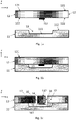
- Figures 1a - 1c illustrate the method.
- the figure illustrates a handle wafer 11 and a device wafer 12. These two wafers may be prepared separately before they are bonded together.
- the handle wafer 11 has a top surface 112.
- a cavity 13 is prepared on the top side of the handle wafer by etching.
- the cavity 13 then has a cavity floor 131 which forms the bottom of the cavity.
- the device wafer 12 has a top surface and a bottom surface 122.
- a bottom coating layer 151 is deposited on the bottom surface 122 of the device wafer 12. This bottom coating layer 151 is positioned so that it is located in a region of the bottom surface 122 which will, in a later stage of the manufacturing process, form the bottom surface of the rotor.
- the bottom surface of the device wafer 12 is bonded to the top surface of the handle wafer 11, for example by fusion bonding.
- the part of the device wafer 12 which comprises the bottom coating layer 151 is aligned with the cavity 13 in the handle wafer 11. Alignment marks may be implemented on the handle wafer and the device wafer to achieve good alignment.
- Figure 1c illustrates the third step of the manufacturing method. Gaps such as 16 are etched in the device wafer 12 to separate the rotor part 14, which will be mobile, from adjacent stator parts in the device wafer, such as 17, whose positions are fixed in relation to the handle wafer.
- the rotor part 14 may be suspended from the stator parts 17 with flexible suspenders which allow the rotor part to undergo movement when it is affected by a force. Suspenders are not illustrated in figure 1c .
- the rotor part 14 has a rotor bottom surface 141 and a rotor top surface 142. As explained above and illustrated in figure 1c , the bottom coating layer 151 was deposited in the region of the device wafer 12 which now forms at least a part of the rotor bottom surface 141.
- the bottom coating layer 151 may cover substantially the entire rotor bottom surface 141.
- the bottom coating layer 151 may cover a middle area on the rotor bottom surface 141, so that the layer 151 is not present on the edges of the rotor bottom surface 141.
- the middle area may be symmetric with respect to the center of gravity of the rotor in the xy-plane.
- the material of the bottom coating layer 151 may for example be gold, copper, silver, tungsten, tantalum, yttrium, neodymium, cerium, lanthanum, zirconium, indium, niobium, molybdenum or hafnium.
- This material may alternatively be a carbide of tungsten, tantalum, yttrium, neodymium, cerium, lanthanum, zirconium, indium, niobium, molybdenum or hafnium, for example WC, TaC x , where x is between 0.4 and 1, YC 2 , NdC 2 , CeC 2 , CeC 2 , ZrC, NbC, Nb 2 C, MoC, Mo 2 C, or HfC.
- the material of the bottom coating layer may be a nitride of tungsten, tantalum, yttrium, neodymium, cerium, lanthanum, zirconium, indium, niobium, molybdenum or hafnium, for example WN, WN2, TaN or HfN.
- the material of the bottom coating layer may be an oxide of tungsten, tantalum or yttrium, for example WO 3 , T12O 5 or Y 2 O 3 .
- nitride-carbide, oxide-carbide or nitride-oxide composite of any element listed above, or a compound material which comprises two or more of the materials listed above.
- the density of the material of the bottom coating layer 151 may be greater than the density of silicon.
- the density of the material of the bottom coating layer 151 may for example be in the range 5 - 50 g/cm 3 , 10 - 50 g/cm 3 or 15 - 30 g/cm 3 .
- the density of the material in coating layer 151 may alternatively be greater than 5 g/cm 3 , greater than 10 g/cm 3 , greater than 15 g/cm 3 , greater than 20 g/cm 3 or greater than 30 g/cm 3 .
- the thickness of the bottom coating layer 151 in the vertical direction may for example be in the range 50 nm - 50 ⁇ m, 500nm - 50 ⁇ m, 1 - 50 ⁇ m, 1 - 10 ⁇ m, 1 - 20 ⁇ m, 10 - 50 ⁇ m, 10 - 30 ⁇ m or 20 - 50 ⁇ m.
- the thickness of the coating layer 151 may alternatively be greater than 50 nm, greater than 500 nm, greater than 1 ⁇ m, greater than 10 ⁇ m, greater than 25 ⁇ m or greater than 50 ⁇ m.
- This disclosure also describes a MEMS component comprising a silicon handle wafer 11 with a top surface 112 which defines a horizontal plane.
- the top surface 112 also defines a vertical direction which is perpendicular to the horizontal plane.
- the MEMS component further comprises a silicon device wafer 12 with a bottom surface 122 and a top surface 121.
- the handle wafer 11 comprises a cavity 13 which is delimited by a cavity floor 131 which is recessed in the vertical direction from the top surface 112 of the handle wafer 11.
- the device wafer 12 comprises a fixed stator part 17 and a mobile rotor part 14.
- the mobile rotor part 14 has a rotor bottom surface 141 and a rotor top surface 142.
- the mobile rotor 14 part is above the cavity floor 131.
- the MEMS component comprises a bottom coating layer 151 which covers at least a part of the rotor bottom surface 141.
- the MEMS component may for example be an accelerometer or a gyroscope.
- the method described above may also comprise the further step of depositing a top coating layer on at least a part of the rotor top surface.
- the MEMS component may comprise a top coating layer which covers at least a part of the rotor top surface.
- Figure 2 illustrates a component where reference number 21 - 24 and 251 correspond to reference numbers 11 - 14 and 151, respectively, in figures 1a - 1d .
- a top coating layer 252 has been deposited on the top surface of the rotor 24.
- the top coating layer 252 may be deposited on the device wafer 22 before the device wafer 22 is bonded to the handle wafer 21, or it may be deposited on the device wafer 22 after the device wafer 22 has been bonded to the handle wafer 21.
- the density of the top coating layer may be greater than the density of the of silicon.
- the center of gravity of the rotor part after the top and bottom coating layers have been deposited may be in the same position where the center of gravity of the rotor part had been if no bottom coating layer and no top coating layer had been deposited on the rotor part.
- the material of the bottom coating layer may be the same as the material of the top coating layer. Furthermore, the vertical thickness of the top coating layer may be substantially equal to the vertical thickness of the bottom coating layer. And finally, the area covered by the bottom coating layer on the rotor bottom surface may be substantially aligned in the vertical direction with the area covered by the top coating layer on the rotor top surface. Any material option listed above for the bottom coating layer can be applied also in the top coating layer. The material of the top coating layer may be different from the material of the bottom coating layer. Furthermore, any density option listed above for the material of the bottom coating layer may apply also to the material of the top coating layer. The density of the top coating layer may be different from the density of the bottom coating layer. Finally, any thickness option listed above for the bottom coating layer may apply also to the top coating layer. The thickness of the top coating layer may be different from the thickness of the bottom coating layer.
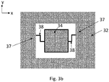
- Figures 3a - 3b illustrate a component where reference numbers 31 - 34 and 37 correspond to reference numbers 11 - 14 and 37, respectively, in figures 1a - 1d .
- the embodiment shown in figures 3a - 3b can also be implemented with the top coating layer which figure 2 illustrates.
- Figures 3a and 3b illustrate a suspension arrangement.
- the rotor part 34 is suspended from stator parts 37 by flexible suspenders 38 which extend from the rotor part to the stator part.
- the suspenders 38 allow the rotor part 34 to move in relation to the stator parts 37, which in this case means motion in relation to the device wafer 32.
- the flexible suspenders may extend from the rotor part to the stator part on at least two sides of the rotor part. These at least two sides may comprise two opposite sides of the rotor, as figures 3a and 3b illustrate. Alternatively, the at least two sides may comprise two sides which are not opposite to each other, or they may comprise three or four sides of the rotor.
- the flexible suspenders 38 may be flexible in the vertical direction (z), so that they allow the rotor part 34 to move in a vertical direction with respect to the stator parts 37.
- the flexible suspenders 38 may be flexible in one or more horizontal directions (x and/or y), so that they allow the rotor part 34 to move in a horizontal direction.
- the flexible suspenders are flexible in all three directions (x,y,z) and allow movement in all of these directions.
Landscapes
- Engineering & Computer Science (AREA)
- Microelectronics & Electronic Packaging (AREA)
- Manufacturing & Machinery (AREA)
- Computer Hardware Design (AREA)
- Gyroscopes (AREA)
- Micromachines (AREA)
Abstract
This disclosure describes a comprising a handle wafer and a device wafer which is bonded to the handle wafer. The handle wafer comprises a cavity and the device wafer comprises a mobile rotor part above the cavity. A bottom coating layer covers at least a part of the bottom surface of the rotor.
Description
- This disclosure relates to micromechanical devices, and particularly to micromechanical devices formed in a device wafer which is bonded to a handle wafer. The present disclosure further concerns the mass of a mobile rotor formed in the device wafer.
- Microelectromechanical (MEMS) devices are typically manufactured from silicon substrates. The micromechanical structures may be formed in a device wafer which has been bonded to a thicker handle wafer for structural support. The micromechanical structures often include a rotor which is mobile in relation to the fixed parts of the device wafer. A cavity can be formed in the region of the handle wafer which will lie beneath the rotor.
- The formation of microelectromechanical structures in the device wafer usually requires gaps which are etched all the way through the device wafer. The deep-etch processes by which such gaps are produced will often leave structural irregularities in these gaps if the device wafer is thick. The likelihood of irregularities will be lower - and the yield of the manufacturing process will consequently be better - if the device wafer is thinner.
- However, very thin device wafers can lead to other challenges in devices such as accelerometers and gyroscopes, where an output signal is produced by measuring the movement of a rotor which has been etched in the device wafer. The output signal becomes more sensitive to small fluctuations in the surrounding environment if the device wafer is very thin and the rotor has a very small mass.
- A rotor with greater surface area will be heavier, but it is typically not a good solution to increase the weight of the rotor by increasing its surface area. The increased area required will also lead to a lower yield when less MEMS chips fit on one device wafer. It would be preferable to use a thin device wafer with a sufficiently heavy rotor without having to increase the surface area of the MEMS chip.
- An object of the present disclosure is to provide an apparatus and method which overcome the above problems.
- The object of the disclosure is achieved by a method and an arrangement which are characterized by what is stated in the independent claims. The preferred embodiments of the disclosure are disclosed in the dependent claims.
- The disclosure is based on the idea of depositing an additional layer on the surface of a rotor in a device wafer before the device wafer is bonded to a handle wafer. This increases the mass of the rotor. An advantage of this arrangement is that a very thin device wafer can be used.
- In the following the disclosure will be described in greater detail by means of preferred embodiments with reference to the accompanying drawings, in which
-
Figures 1a - 1c illustrate a MEMS component where the bottom surface of the rotor is coated, and a method for manufacturing such a component. -
Figure 1d illustrates a bottom coating layer which covers a symmetric middle area on the rotor bottom surface. -
Figure 2 illustrates illustrate a MEMS component where both the top and the bottom surfaces of the rotor are coated. -
Figures 3a - 3b illustrate a suspension arrangement. - This disclosure relates to method for manufacturing a MEMS component. The method comprises the steps of (1) forming a cavity on a top surface of a silicon handle wafer, (2) bonding a bottom surface of a silicon device wafer onto the top surface of the handle wafer so that the device wafer covers the cavity, and (3) forming microelectromechanical structures comprising a fixed stator part and a mobile rotor part in the device wafer. The mobile rotor part has a rotor bottom surface and a rotor top surface. The mobile rotor part is suspended from the fixed stator part above the cavity. The method also comprises the step of depositing a bottom coating layer on at least a part of the rotor bottom surface before the device wafer is bonded to the handle wafer.
- In this disclosure, the surfaces of the device wafer and the handle wafer define an xy-plane which may be referred to as the device plane. The direction which is perpendicular to the device plane is illustrated with the z-axis and referred to as the vertical direction. Words such as "top" and "bottom" refer to vertically separated sides. These words do not imply anything about how the MEMS device should be oriented during usage or during manufacturing. The word "thickness" refers in this disclosure to the z-dimension.
-
Figures 1a - 1c illustrate the method. The figure illustrates ahandle wafer 11 and a device wafer 12. These two wafers may be prepared separately before they are bonded together. Thehandle wafer 11 has atop surface 112. Acavity 13 is prepared on the top side of the handle wafer by etching. Thecavity 13 then has acavity floor 131 which forms the bottom of the cavity. - The
device wafer 12 has a top surface and abottom surface 122. Abottom coating layer 151 is deposited on thebottom surface 122 of the device wafer 12. Thisbottom coating layer 151 is positioned so that it is located in a region of thebottom surface 122 which will, in a later stage of the manufacturing process, form the bottom surface of the rotor. - In the next method step, illustrated in
figure 1b , the bottom surface of thedevice wafer 12 is bonded to the top surface of thehandle wafer 11, for example by fusion bonding. The part of thedevice wafer 12 which comprises thebottom coating layer 151 is aligned with thecavity 13 in thehandle wafer 11. Alignment marks may be implemented on the handle wafer and the device wafer to achieve good alignment. -
Figure 1c illustrates the third step of the manufacturing method. Gaps such as 16 are etched in thedevice wafer 12 to separate therotor part 14, which will be mobile, from adjacent stator parts in the device wafer, such as 17, whose positions are fixed in relation to the handle wafer. In practice, therotor part 14 may be suspended from thestator parts 17 with flexible suspenders which allow the rotor part to undergo movement when it is affected by a force. Suspenders are not illustrated infigure 1c . - The
rotor part 14 has arotor bottom surface 141 and arotor top surface 142. As explained above and illustrated infigure 1c , thebottom coating layer 151 was deposited in the region of thedevice wafer 12 which now forms at least a part of therotor bottom surface 141. - The
bottom coating layer 151 may cover substantially the entirerotor bottom surface 141. Alternatively, as illustrated infigure 1d , thebottom coating layer 151 may cover a middle area on therotor bottom surface 141, so that thelayer 151 is not present on the edges of therotor bottom surface 141. The middle area may be symmetric with respect to the center of gravity of the rotor in the xy-plane. - The material of the
bottom coating layer 151 may for example be gold, copper, silver, tungsten, tantalum, yttrium, neodymium, cerium, lanthanum, zirconium, indium, niobium, molybdenum or hafnium. This material may alternatively be a carbide of tungsten, tantalum, yttrium, neodymium, cerium, lanthanum, zirconium, indium, niobium, molybdenum or hafnium, for example WC, TaCx, where x is between 0.4 and 1, YC2, NdC2, CeC2, CeC2, ZrC, NbC, Nb2C, MoC, Mo2C, or HfC. As a further alternative, the material of the bottom coating layer may be a nitride of tungsten, tantalum, yttrium, neodymium, cerium, lanthanum, zirconium, indium, niobium, molybdenum or hafnium, for example WN, WN2, TaN or HfN. Finally, the material of the bottom coating layer may be an oxide of tungsten, tantalum or yttrium, for example WO3, T12O5 or Y2O3. It could alternatively be a nitride-carbide, oxide-carbide or nitride-oxide composite of any element listed above, or a compound material which comprises two or more of the materials listed above. These material options apply to all coating layers (top and bottom) described in this disclosure. - The density of the material of the
bottom coating layer 151 may be greater than the density of silicon. The density of the material of thebottom coating layer 151 may for example be in the range 5 - 50 g/cm3, 10 - 50 g/cm3 or 15 - 30 g/cm3. The density of the material incoating layer 151 may alternatively be greater than 5 g/cm3, greater than 10 g/cm3, greater than 15 g/cm3, greater than 20 g/cm3 or greater than 30 g/cm3. The thickness of thebottom coating layer 151 in the vertical direction may for example be in the range 50 nm - 50 µm, 500nm - 50 µm, 1 - 50 µm, 1 - 10 µm, 1 - 20 µm, 10 - 50 µm, 10 - 30 µm or 20 - 50 µm. The thickness of thecoating layer 151 may alternatively be greater than 50 nm, greater than 500 nm, greater than 1 µm, greater than 10 µm, greater than 25 µm or greater than 50 µm. These density and thickness options apply to all coating layers (top and bottom) described in this disclosure. Any thickness option listed above can be combined with any density option listed above. Any thickness option listed above can also be combined with any material option listed above. - This disclosure also describes a MEMS component comprising a
silicon handle wafer 11 with atop surface 112 which defines a horizontal plane. Thetop surface 112 also defines a vertical direction which is perpendicular to the horizontal plane. The MEMS component further comprises asilicon device wafer 12 with abottom surface 122 and atop surface 121. - The
handle wafer 11 comprises acavity 13 which is delimited by acavity floor 131 which is recessed in the vertical direction from thetop surface 112 of thehandle wafer 11. Thedevice wafer 12 comprises a fixedstator part 17 and amobile rotor part 14. Themobile rotor part 14 has arotor bottom surface 141 and a rotortop surface 142. Themobile rotor 14 part is above thecavity floor 131. The MEMS component comprises abottom coating layer 151 which covers at least a part of therotor bottom surface 141. - The MEMS component may for example be an accelerometer or a gyroscope.
- The method described above may also comprise the further step of depositing a top coating layer on at least a part of the rotor top surface. Correspondingly, the MEMS component may comprise a top coating layer which covers at least a part of the rotor top surface.
-
Figure 2 illustrates a component where reference number 21 - 24 and 251 correspond to reference numbers 11 - 14 and 151, respectively, infigures 1a - 1d . Atop coating layer 252 has been deposited on the top surface of therotor 24. Thetop coating layer 252 may be deposited on thedevice wafer 22 before thedevice wafer 22 is bonded to thehandle wafer 21, or it may be deposited on thedevice wafer 22 after thedevice wafer 22 has been bonded to thehandle wafer 21. The density of the top coating layer may be greater than the density of the of silicon. - It will in some cases be beneficial to make the top coating layer symmetric with the bottom coating layer. The center of gravity of the rotor part after the top and bottom coating layers have been deposited may be in the same position where the center of gravity of the rotor part had been if no bottom coating layer and no top coating layer had been deposited on the rotor part.
- The material of the bottom coating layer may be the same as the material of the top coating layer. Furthermore, the vertical thickness of the top coating layer may be substantially equal to the vertical thickness of the bottom coating layer. And finally, the area covered by the bottom coating layer on the rotor bottom surface may be substantially aligned in the vertical direction with the area covered by the top coating layer on the rotor top surface. Any material option listed above for the bottom coating layer can be applied also in the top coating layer. The material of the top coating layer may be different from the material of the bottom coating layer. Furthermore, any density option listed above for the material of the bottom coating layer may apply also to the material of the top coating layer. The density of the top coating layer may be different from the density of the bottom coating layer. Finally, any thickness option listed above for the bottom coating layer may apply also to the top coating layer. The thickness of the top coating layer may be different from the thickness of the bottom coating layer.
-
Figures 3a - 3b illustrate a component where reference numbers 31 - 34 and 37 correspond to reference numbers 11 - 14 and 37, respectively, infigures 1a - 1d . The embodiment shown infigures 3a - 3b can also be implemented with the top coating layer whichfigure 2 illustrates. -
Figures 3a and3b illustrate a suspension arrangement. Therotor part 34 is suspended fromstator parts 37 byflexible suspenders 38 which extend from the rotor part to the stator part. Thesuspenders 38 allow therotor part 34 to move in relation to thestator parts 37, which in this case means motion in relation to thedevice wafer 32. The flexible suspenders may extend from the rotor part to the stator part on at least two sides of the rotor part. These at least two sides may comprise two opposite sides of the rotor, asfigures 3a and3b illustrate. Alternatively, the at least two sides may comprise two sides which are not opposite to each other, or they may comprise three or four sides of the rotor. - The
flexible suspenders 38 may be flexible in the vertical direction (z), so that they allow therotor part 34 to move in a vertical direction with respect to thestator parts 37. Alternatively, theflexible suspenders 38 may be flexible in one or more horizontal directions (x and/or y), so that they allow therotor part 34 to move in a horizontal direction. Another alternative is that the flexible suspenders are flexible in all three directions (x,y,z) and allow movement in all of these directions.
Claims (12)
- A MEMS component comprising a silicon handle wafer with a top surface which defines a horizontal plane, whereby the top surface also defines a vertical direction which is perpendicular to the horizontal plane, and the MEMS component further comprises a silicon device wafer with a bottom surface and a top surface,and the handle wafer comprises a cavity which is delimited by a cavity floor which is recessed in the vertical direction from the top surface of the handle wafer,and the device wafer comprises a fixed stator part and a mobile rotor part, wherein the mobile rotor part has a rotor bottom surface and a rotor top surface, and the mobile rotor part is above the cavity floor,characterized in that the MEMS component comprises a bottom coating layer which covers at least a part of the rotor bottom surface.
- A MEMS component according to claim 1, characterized in that the density of the material of the bottom coating layer is greater than the density of silicon.
- A MEMS component according to any of claims 1-2, characterized in that the MEMS component also comprises a top coating layer which covers at least a part of the rotor top surface.
- A MEMS component according to claim 3, characterized in that the the density of the material of the top coating layer is greater than the density of silicon.
- A MEMS component according to any of claims 3-4, characterized in that the material of the bottom coating layer is the same as the material of the top coating layer.
- A MEMS component according to claim 5, characterized in that the vertical thickness of the top coating layer is substantially equal to the vertical thickness of the bottom coating layer, and the area covered by the bottom coating layer on the rotor bottom surface is substantially aligned in the vertical direction with the area covered by the top coating layer on the rotor top surface.
- A method for manufacturing a MEMS component comprising the steps of- forming a cavity on a top surface of a silicon handle wafer- bonding a bottom surface of a silicon device wafer onto the top surface of the handle wafer so that the device wafer covers the cavity,- forming microelectromechanical structures comprising a fixed stator part and a mobile rotor part in the device wafer, wherein the mobile rotor part has a rotor bottom surface and a rotor top surface, and the mobile rotor part is suspended from the fixed stator part above the cavity,characterized in that the method further comprises the step of:- depositing a bottom coating layer on at least a part of the rotor bottom surface before the device wafer is bonded to the handle wafer.
- A method according to claim 6, characterized in that the the density of the material of the bottom coating layer is greater than the density of silicon.
- A method according to any of claims 6-7, characterized in that the method further comprises the step of depositing a top coating layer on at least a part of the rotor top surface.
- A method according to claim 8, characterized in that the the density of the material of the top coating layer is greater than the density of silicon.
- A method according to any of claims 8-9, characterized in that the material of the bottom coating layer is the same as the material of the top coating layer.
- A method according to claim 11, characterized in that the thickness of the top coating layer is substantially equal to the thickness of the bottom coating layer and the area covered by the bottom coating layer on the rotor bottom surface is substantially aligned in the vertical direction with the area covered by the top coating layer on the rotor top surface.
Applications Claiming Priority (1)
| Application Number | Priority Date | Filing Date | Title |
|---|---|---|---|
| FI20215470 | 2021-04-22 |
Publications (1)
| Publication Number | Publication Date |
|---|---|
| EP4079678A1 true EP4079678A1 (en) | 2022-10-26 |
Family
ID=80448675
Family Applications (1)
| Application Number | Title | Priority Date | Filing Date |
|---|---|---|---|
| EP22158410.5A Pending EP4079678A1 (en) | 2021-04-22 | 2022-02-24 | Mems rotor with coated bottom surface |
Country Status (3)
| Country | Link |
|---|---|
| US (1) | US20220340411A1 (en) |
| EP (1) | EP4079678A1 (en) |
| JP (1) | JP7444185B2 (en) |
Citations (1)
| Publication number | Priority date | Publication date | Assignee | Title |
|---|---|---|---|---|
| US20080018975A1 (en) * | 2006-07-18 | 2008-01-24 | Moidu Abdul Jaleel K | MEMS Device with a Closed Cellular Core Sandwiched Structure |
Family Cites Families (8)
| Publication number | Priority date | Publication date | Assignee | Title |
|---|---|---|---|---|
| JP3234652B2 (en) * | 1992-10-14 | 2001-12-04 | キヤノン株式会社 | Acceleration sensor and method of manufacturing the same |
| US6618184B2 (en) * | 2001-04-03 | 2003-09-09 | Agere Systems Inc. | Device for use with a micro-electro-mechanical system (MEMS) optical device and a method of manufacture therefor |
| US6639724B2 (en) * | 2001-06-05 | 2003-10-28 | Lucent Technologies Inc. | Device having a barrier layer located therein and a method of manufacture therefor |
| JP4994098B2 (en) * | 2007-04-25 | 2012-08-08 | 株式会社リコー | Semiconductor sensor and manufacturing method thereof |
| JP5058879B2 (en) * | 2008-05-19 | 2012-10-24 | 株式会社ミツトヨ | MEMS acceleration sensor |
| JP2010117247A (en) * | 2008-11-13 | 2010-05-27 | Alps Electric Co Ltd | Mems sensor and method for manufacturing the same |
| DE102009026738A1 (en) * | 2009-06-04 | 2010-12-09 | Robert Bosch Gmbh | Micromechanical acceleration sensor and method for producing an acceleration sensor |
| DE102020116511B4 (en) * | 2020-06-23 | 2022-03-24 | OQmented GmbH | Glass substrate based MEMS mirror device and method for its manufacture |
-
2022
- 2022-02-24 EP EP22158410.5A patent/EP4079678A1/en active Pending
- 2022-03-18 JP JP2022043634A patent/JP7444185B2/en active Active
- 2022-04-20 US US17/725,411 patent/US20220340411A1/en not_active Abandoned
Patent Citations (1)
| Publication number | Priority date | Publication date | Assignee | Title |
|---|---|---|---|---|
| US20080018975A1 (en) * | 2006-07-18 | 2008-01-24 | Moidu Abdul Jaleel K | MEMS Device with a Closed Cellular Core Sandwiched Structure |
Also Published As
| Publication number | Publication date |
|---|---|
| JP7444185B2 (en) | 2024-03-06 |
| US20220340411A1 (en) | 2022-10-27 |
| JP2022167792A (en) | 2022-11-04 |
Similar Documents
| Publication | Publication Date | Title |
|---|---|---|
| US8372677B2 (en) | Three-axis accelerometers and fabrication methods | |
| CN102718179B (en) | MEMS devices and manufacture method thereof | |
| KR100907514B1 (en) | Sensor device, sensor system and method of manufacturing the same | |
| US7863698B2 (en) | Performance-enhancing two-sided MEMS anchor design for vertically integrated micromachined devices | |
| US20020146200A1 (en) | Electrostatically actuated micro-electro-mechanical devices and method of manufacture | |
| US20110049652A1 (en) | Method and system for mems devices | |
| WO2014171896A1 (en) | Electromechanical device and method of fabricating the same | |
| US20130032385A1 (en) | Metal thin shield on electrical device | |
| CN102388165B (en) | MEMS devices with integrated vias and compartments | |
| CN101597021B (en) | Method for structuring a device layer of a substrate | |
| US20220340411A1 (en) | Mems rotor with coated bottom surface | |
| US10184951B2 (en) | Three-axis monolithic MEMS accelerometers and methods for fabricating same | |
| EP3816100B1 (en) | Mems element with increased density | |
| CN113551672A (en) | Microelectromechanical system, MEMS inertial sensor, and manufacturing method thereof | |
| TWI693191B (en) | Substrate structure for mems device and method of fabricating semiconductor structure | |
| US11731871B2 (en) | Actuator layer patterning with polysilicon and etch stop layer | |
| US12017909B2 (en) | Fabrication method for a MEMS device | |
| CN209721578U (en) | A piezoresistive dual-axis motion sensor | |
| CN110002395B (en) | A piezoresistive dual-axis motion sensor and a manufacturing method thereof | |
| TWI850094B (en) | Micro-electro-mechanical system package and fabrication method thereof | |
| EP4628444A1 (en) | Method for bonding wafers | |
| JP2006026895A (en) | Vertical step structure and manufacturing method thereof | |
| CN119568984A (en) | Microelectromechanical package and method of manufacturing the same | |
| EP3121561B1 (en) | Sensor | |
| JP2010153426A (en) | Mems and manufacturing method thereof |
Legal Events
| Date | Code | Title | Description |
|---|---|---|---|
| PUAI | Public reference made under article 153(3) epc to a published international application that has entered the european phase |
Free format text: ORIGINAL CODE: 0009012 |
|
| STAA | Information on the status of an ep patent application or granted ep patent |
Free format text: STATUS: REQUEST FOR EXAMINATION WAS MADE |
|
| 17P | Request for examination filed |
Effective date: 20220224 |
|
| AK | Designated contracting states |
Kind code of ref document: A1 Designated state(s): AL AT BE BG CH CY CZ DE DK EE ES FI FR GB GR HR HU IE IS IT LI LT LU LV MC MK MT NL NO PL PT RO RS SE SI SK SM TR |
|
| STAA | Information on the status of an ep patent application or granted ep patent |
Free format text: STATUS: EXAMINATION IS IN PROGRESS |
|
| 17Q | First examination report despatched |
Effective date: 20250417 |