EP4075657A1 - Power conversion device - Google Patents
Power conversion device Download PDFInfo
- Publication number
- EP4075657A1 EP4075657A1 EP19955445.2A EP19955445A EP4075657A1 EP 4075657 A1 EP4075657 A1 EP 4075657A1 EP 19955445 A EP19955445 A EP 19955445A EP 4075657 A1 EP4075657 A1 EP 4075657A1
- Authority
- EP
- European Patent Office
- Prior art keywords
- negative
- positive
- switching element
- side busbar
- capacitor
- Prior art date
- Legal status (The legal status is an assumption and is not a legal conclusion. Google has not performed a legal analysis and makes no representation as to the accuracy of the status listed.)
- Pending
Links
Images






Classifications
-
- H—ELECTRICITY
- H02—GENERATION; CONVERSION OR DISTRIBUTION OF ELECTRIC POWER
- H02M—APPARATUS FOR CONVERSION BETWEEN AC AND AC, BETWEEN AC AND DC, OR BETWEEN DC AND DC, AND FOR USE WITH MAINS OR SIMILAR POWER SUPPLY SYSTEMS; CONVERSION OF DC OR AC INPUT POWER INTO SURGE OUTPUT POWER; CONTROL OR REGULATION THEREOF
- H02M7/00—Conversion of AC power input into DC power output; Conversion of DC power input into AC power output
- H02M7/42—Conversion of DC power input into AC power output without possibility of reversal
- H02M7/44—Conversion of DC power input into AC power output without possibility of reversal by static converters
- H02M7/48—Conversion of DC power input into AC power output without possibility of reversal by static converters using discharge tubes with control electrode or semiconductor devices with control electrode
- H02M7/483—Converters with outputs that each can have more than two voltages levels
- H02M7/4835—Converters with outputs that each can have more than two voltages levels comprising two or more cells, each including a switchable capacitor, the capacitors having a nominal charge voltage which corresponds to a given fraction of the input voltage, and the capacitors being selectively connected in series to determine the instantaneous output voltage
-
- H—ELECTRICITY
- H02—GENERATION; CONVERSION OR DISTRIBUTION OF ELECTRIC POWER
- H02M—APPARATUS FOR CONVERSION BETWEEN AC AND AC, BETWEEN AC AND DC, OR BETWEEN DC AND DC, AND FOR USE WITH MAINS OR SIMILAR POWER SUPPLY SYSTEMS; CONVERSION OF DC OR AC INPUT POWER INTO SURGE OUTPUT POWER; CONTROL OR REGULATION THEREOF
- H02M1/00—Details of apparatus for conversion
- H02M1/0067—Converter structures employing plural converter units, other than for parallel operation of the units on a single load
- H02M1/007—Plural converter units in cascade
-
- H—ELECTRICITY
- H02—GENERATION; CONVERSION OR DISTRIBUTION OF ELECTRIC POWER
- H02M—APPARATUS FOR CONVERSION BETWEEN AC AND AC, BETWEEN AC AND DC, OR BETWEEN DC AND DC, AND FOR USE WITH MAINS OR SIMILAR POWER SUPPLY SYSTEMS; CONVERSION OF DC OR AC INPUT POWER INTO SURGE OUTPUT POWER; CONTROL OR REGULATION THEREOF
- H02M3/00—Conversion of DC power input into DC power output
- H02M3/02—Conversion of DC power input into DC power output without intermediate conversion into AC
- H02M3/04—Conversion of DC power input into DC power output without intermediate conversion into AC by static converters
- H02M3/10—Conversion of DC power input into DC power output without intermediate conversion into AC by static converters using discharge tubes with control electrode or semiconductor devices with control electrode
- H02M3/145—Conversion of DC power input into DC power output without intermediate conversion into AC by static converters using discharge tubes with control electrode or semiconductor devices with control electrode using devices of a triode or transistor type requiring continuous application of a control signal
- H02M3/155—Conversion of DC power input into DC power output without intermediate conversion into AC by static converters using discharge tubes with control electrode or semiconductor devices with control electrode using devices of a triode or transistor type requiring continuous application of a control signal using semiconductor devices only
- H02M3/156—Conversion of DC power input into DC power output without intermediate conversion into AC by static converters using discharge tubes with control electrode or semiconductor devices with control electrode using devices of a triode or transistor type requiring continuous application of a control signal using semiconductor devices only with automatic control of output voltage or current, e.g. switching regulators
-
- H—ELECTRICITY
- H02—GENERATION; CONVERSION OR DISTRIBUTION OF ELECTRIC POWER
- H02M—APPARATUS FOR CONVERSION BETWEEN AC AND AC, BETWEEN AC AND DC, OR BETWEEN DC AND DC, AND FOR USE WITH MAINS OR SIMILAR POWER SUPPLY SYSTEMS; CONVERSION OF DC OR AC INPUT POWER INTO SURGE OUTPUT POWER; CONTROL OR REGULATION THEREOF
- H02M7/00—Conversion of AC power input into DC power output; Conversion of DC power input into AC power output
- H02M7/003—Constructional details, e.g. physical layout, assembly, wiring or busbar connections
Definitions
- the present invention relates to a power conversion device.
- a modular multilevel converter is of a circuit type in which output terminals of cell converters each composed of a DC capacitor and a switching element capable of being controlled to be turned on/off such as an IGBT are connected in series so that a high voltage higher than a withstanding voltage of the switching element can be outputted.
- the MMC is expected to be applied to DC power transmission systems (HVDCs), reactive power compensation devices (STATCOMs), and the like.
- HVDCs DC power transmission systems
- STATCOMs reactive power compensation devices
- an MMC is formed by connecting a plurality of cell converters in series (cascade). Each cell converter is composed of: a main circuit composed of a switching element and a DC capacitor; and an external terminal for cascade connection to another one of the cell converters. An external conductor is used for bridge connection between the switching elements.
- Patent Document 2 has the following drawback. That is, if DC capacitors are additionally provided from the state in FIG. 3 to the state in FIG. 7 in Patent Document 2, the width of a cell converter is increased in an arrangement configuration of a power conversion device intended for HVDCs. Considering this, the number of the cell converters that can be accommodated in a cell converter accommodation frame has to be decreased, or the horizontal dimension of the cell converter accommodation frame has to be increased.
- the present invention has been made to solve the above drawback, and an object of the present invention is to obtain a power conversion device in which the magnitudes of currents flowing to respective DC capacitors are set to be equal to one another; and the width of a cell converter does not increase even if the number of the DC capacitors that are used in parallel is increased.
- a power conversion device includes: a first switching element and a second switching element each having a positive terminal and a negative terminal; and a plurality of DC capacitors each having a positive terminal and a negative terminal.
- the negative terminal of the first switching element and the positive terminal of the second switching element are connected to each other.
- Each of the plurality of DC capacitors is connected in parallel between the positive terminal of the first switching element and the negative terminal of the second switching element.
- the first switching element, the second switching element, and the plurality of DC capacitors are disposed in this order or the second switching element, the first switching element, and the plurality of DC capacitors are disposed in this order, such that all of the positive terminals and the negative terminals are aligned on a same side.
- a plurality of positive-side busbars are provided, the number of the positive-side busbars being equal to the number of the DC capacitors, each positive-side busbar connecting the positive terminal of the first switching element and the positive terminal of a corresponding one of the plurality of DC capacitors to each other.
- a plurality of negative-side busbars are provided, the number of the negative-side busbars being equal to the number of the DC capacitors, each negative-side busbar connecting the negative terminal of the second switching element and the negative terminal of a corresponding one of the plurality of DC capacitors to each other.
- An adjustment positive-side busbar which is a positive-side busbar among the plurality of positive-side busbars other than the positive-side busbar connected to the DC capacitor farthest from the first switching element, has an inductance adjustment portion providing a bypass such that a length on the adjustment positive-side busbar between the positive terminal of the first switching element and the positive terminal of the DC capacitor to which the adjustment positive-side busbar is connected, is longer than a straight distance between the positive terminal of the first switching element and the positive terminal of the DC capacitor to which the adjustment positive-side busbar is connected.
- An adjustment negative-side busbar which is a negative-side busbar among the plurality of negative-side busbars other than the negative-side busbar connected to the DC capacitor farthest from the second switching element, has an inductance adjustment portion providing a bypass such that a length on the adjustment negative-side busbar between the negative terminal of the second switching element and the negative terminal of the DC capacitor to which the adjustment negative-side busbar is connected, is longer than a straight distance between the negative terminal of the second switching element and the negative terminal of the DC capacitor to which the adjustment negative-side busbar is connected.
- the power conversion device leads to obtainment of a power conversion device in which: the magnitudes of currents flowing to respective DC capacitors are set to be equal to one another; and the width of a cell converter does not increase even if the number of the DC capacitors that are used in parallel is increased.
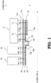
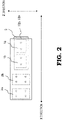
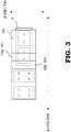
- FIG. 1 to FIG. 3 are schematic diagrams showing a component configuration of a power conversion device according to Embodiment 1.
- FIG. 1 is a top view
- FIG. 2 and FIG. 3 are side views.
- FIG. 2 is a side view in which some busbars are excluded from busbars shown in the top view in FIG. 1 .
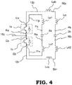
- FIG. 4 is a circuit diagram showing an equivalent circuit of the power conversion device shown in FIG. 1 to FIG. 3 . That is, FIG. 1 to FIG. 3 are schematic diagrams in which components on the circuit shown in FIG. 4 are disposed.
- the power conversion device is a power conversion device including: a first switching element 1a in which a first switch and a first diode connected in antiparallel to the first switch are mounted; a second switching element 1b in which a second switch and a second diode connected in antiparallel to the second switch are mounted; a first DC capacitor 2a; a second DC capacitor 2b; and a cooler 3 which is mounted with the first switching element 1a and the second switching element 1b and which cools the switching elements.
- the first switching element 1a and the second switching element 1b are mounted on a flat surface portion of the cooler 3 by means of fixation members such as screws so as to be parallel to the shape of the cooler 3 in an X direction.
- the first switching element 1a, the second switching element 1b, the first DC capacitor 2a, and the second DC capacitor 2b have respective positive terminals and respective negative terminals, and are disposed to be aligned in the X direction such that all of the positive terminals and the negative terminals are on a same side.
- the first switching element 1a and the second switching element 1b are disposed to be adjacent to each other, and the first DC capacitor 2a and the second DC capacitor 2b are disposed to be adjacent to each other.
- the DC capacitor disposed farther from the switching elements is defined as the first DC capacitor 2a.
- a midpoint busbar 10c makes bridge connection between a negative terminal Ea of the first switching element 1a and a positive terminal Cb of the second switching element 1b.
- a positive terminal Ca of the first switching element 1a and a positive terminal Pa of the first DC capacitor 2a are electrically connected to each other by a first positive-side busbar 11p, and the positive terminal Ca of the first switching element 1a and a positive terminal Pb of the second DC capacitor 2b are electrically connected to each other by a second positive-side busbar 12p.
- a negative terminal Eb of the second switching element 1b and a negative terminal Na of the first DC capacitor 2a are electrically connected to each other by a first negative-side busbar 11n, and the negative terminal Eb of the second switching element 1b and a negative terminal Nb of the second DC capacitor 2b are electrically connected to each other by a second negative-side busbar 12n.
- the second positive-side busbar 12p has an inductance adjustment portion 32p providing a bypass such that a length on the second positive-side busbar 12p between the positive terminal Ca of the first switching element 1a and the positive terminal Pb of the second DC capacitor 2b is longer than a straight distance between the positive terminal Ca of the first switching element 1a and the positive terminal Pb of the second DC capacitor 2b.
- the second positive-side busbar 12p having the inductance adjustment portion 32p is sometimes referred to also as an adjustment positive-side busbar 12p.
- the second negative-side busbar 12n has an inductance adjustment portion 32n providing a bypass such that a length on the second negative-side busbar 12n between the negative terminal Eb of the second switching element 1b and the negative terminal Nb of the second DC capacitor 2b is longer than a straight distance between the negative terminal Eb of the second switching element 1b and the negative terminal Nb of the second DC capacitor 2b.
- the second negative-side busbar 12n having the inductance adjustment portion 32n is sometimes referred to also as an adjustment negative-side busbar 12n.
- Each busbar is formed of, for example, a sheet-shaped metal.
- the positive-side busbar and the negative-side busbar which are connected to each DC capacitor, are disposed in a superposed manner such that sheet surfaces of the busbars face each other with an insulating member 40 (indicated by an alternate long and short dash line) being interposed therebetween.
- the first positive-side busbar 11p and the first negative-side busbar 11n are disposed in a superposed manner with an insulating member 40 being interposed therebetween
- the second positive-side busbar 12p and the second negative-side busbar 12n are disposed in a superposed manner with an insulating member 40 being interposed therebetween.
- the set of two busbars connected to the first DC capacitor 2a and the set of two busbars connected to the second DC capacitor 2b may be disposed in a superposed manner with an insulating member 40 being interposed between the sets.
- the first negative-side busbar 11n is disposed closer to the switching elements and the DC capacitors than the first positive-side busbar 11p is, the positions of these busbars may be reversed.
- the second negative-side busbar 12n is disposed closer to the switching elements and the DC capacitors than the second positive-side busbar 12p is, the positions of these busbars may be reversed.
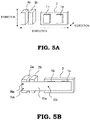
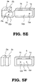
- FIG. 5A to FIG. 5F are perspective views showing the states of the busbars in an easily understandable manner.
- FIG. 5A shows a state where no busbar is present.
- FIG. 5B shows a state where the negative terminal Eb of the second switching element 1b and the negative terminal Na of the first DC capacitor 2a are connected to each other by the first negative-side busbar 11n.
- FIG. 5C shows a state where the positive terminal Ca of the first switching element 1a and the positive terminal Pa of the first DC capacitor 2a are connected to each other by the first positive-side busbar 11p.
- FIG. 5D shows a state where the negative terminal Eb of the second switching element 1b and the negative terminal Nb of the second DC capacitor 2b are connected to each other by the second negative-side busbar 12n having the inductance adjustment portion 32n.
- FIG. 5E shows a state where the positive terminal Ca of the first switching element 1a and the positive terminal Pb of the second DC capacitor 2b are connected to each other by the second positive-side busbar 12p having the inductance adjustment portion 32p.
- FIG. 5F shows a state where the negative terminal Ea of the first switching element 1a and the positive terminal Cb of the second switching element 1b are connected to each other by the midpoint busbar 10c.
- FIG. 6 is a schematic diagram showing another component configuration of the power conversion device according to Embodiment 1.
- the sequences of the positive terminals and the negative terminals of the DC capacitors are not limited to the sequences in FIG. 1 , and the positive terminals may be located farther from the switching elements as shown in FIG. 6 .
- the sequence of the positive terminal and the negative terminal is preferably the same between the DC capacitors.
- the sequence of the positive terminal and the negative terminal is preferably the same between the first DC capacitor 2a and the second DC capacitor 2b such that the difference between the distance from the positive terminal Ca of the first switching element 1a to the positive terminal Pa of the first DC capacitor 2a and the distance from the positive terminal Ca of the first switching element 1a to the positive terminal Pb of the second DC capacitor 2b is equal to the difference between the distance from the negative terminal Eb of the second switching element 1b to the negative terminal Na of the first DC capacitor 2a and the distance from the negative terminal Eb of the second switching element 1b to the negative terminal Nb of the second DC capacitor 2b.
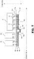
- FIG. 7 is a schematic diagram showing still another component configuration of the power conversion device according to Embodiment 1.
- either of the first switching element 1a and the second switching element 1b may be disposed closer to the DC capacitors as long as the negative terminal Ea of the first switching element 1a and the positive terminal Cb of the second switching element 1b are connected to each other. Further, regarding the switching elements, the sequence of the positive terminal and the negative terminal may be reversed between the switching elements.
- sequence of the first switching element 1a and the second switching element 1b and the sequence of the positive terminal and the negative terminal thereof are not limited in terms of order. Meanwhile, the sequence of the positive terminal and the negative terminal is preferably the same between the first DC capacitor 2a and the second DC capacitor 2b.
- Wiring inductances shown in the equivalent circuit in FIG. 4 are present between the terminals on the busbars. Specifically, a wiring inductance Lp1 is present on the first positive-side busbar 11p, a wiring inductance Ln1 is present on the first negative-side busbar 11n, a wiring inductance Lpb of the inductance adjustment portion 32p and another wiring inductance Lp2 are present on the second positive-side busbar 12p, and a wiring inductance Lnb of the inductance adjustment portion 32n and another wiring inductance Ln2 are present on the second negative-side busbar 12n.
- the lengths of the inductance adjustment portions are adjusted such that: the wiring inductances on the second positive-side busbar (adjustment positive-side busbar) 12p, i.e., the wiring inductance Lp2 and the wiring inductance Lpb of the inductance adjustment portion 32p, are equal to the wiring inductance Lp1 on the first positive-side busbar; and the wiring inductances on the second negative-side busbar (adjustment negative-side busbar) 12n, i.e., the wiring inductance Ln2 and the wiring inductance Lnb of the inductance adjustment portion 32n, are equal to the wiring inductance Ln1 on the first negative-side busbar. That is, in the inductance adjustment portion 32p and the inductance adjustment portion 32n, the lengths from the switching elements to the DC capacitors are adjusted by bending or curving the in
- the above busbar configuration leads to presence of two busbars in which different currents flow through: a path between each switching element and the first DC capacitor 2a; and a path between the switching element and the second DC capacitor 2b. Consequently, the value of current flowing in each busbar is half the value in a conventional busbar configuration and, with a thickness dimension being equal to a conventional thickness dimension, heat generated from the busbar at the same level of current is lower than in the conventional busbar configuration, whereby output current of the power conversion device can be increased.
- the thickness dimension of each busbar can be set to half the conventional thickness dimension.
- machining work such as bending of the busbars becomes easy, and the weight of each single busbar is decreased, whereby assembling work becomes easy.
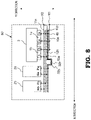
- FIG. 8 is a schematic diagram showing a configuration in a case where the power conversion device according to Embodiment 1 is configured as a cell converter 60.
- FIG. 9 is a diagram showing an equivalent circuit of the cell converter 60.
- FIG. 8 and FIG. 9 are different from FIG. 1 and FIG. 4 in that: an external terminal X1 is provided at a position, on the midpoint busbar 10c, that is an end portion of the cell converter 60; and an external terminal X2 is provided at a position that is an end portion of the cell converter 60 and at which the first negative-side busbar 11n and the second negative-side busbar 12n are connected to each other.
- the external terminal X1 and the external terminal X2 are located on a front side of the cell converter 60.
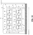
- FIG. 10 is a schematic diagram showing an arrangement configuration of a general power conversion device intended for HVDCs and shows a connection configuration in which a plurality of cell converters 60 each of which is the cell converter 60 shown in FIG. 8 are used.
- the plurality of cell converters 60 are aligned in a horizontal Y direction and accommodated in one cell converter housing 61.
- FIG. 10 shows an example in which four cell converters 60 are accommodated in one cell converter housing 61.
- each cell converter 60 has the external terminal X1 and the external terminal X2.
- the external terminal X1 of the cell converter 60 and the external terminal X2 of another cell converter 60 adjacent thereto are connected to each other via an inter-cell-converter connection conductor 62, and the external terminal X2 of the other cell converter 60 and the external terminal X1 of still another cell converter 60 adjacent thereto are connected to each other via an inter-cell-converter connection conductor 62, whereby the plurality of cell converters 60 are connected in series.
- valve 63 This component in which the plurality of cell converters 60 accommodated in the cell converter housing 61 are connected in series, i.e., connected in cascade, is referred to as a valve 63.
- a plurality of the valves 63 are stacked in the vertical direction (height direction, Z direction) and connected to each other via an inter-valve connection conductor 64 so that the number of the cell converters 60 that are connected in series can be set to be further larger than in a configuration provided with only one valve.
- Insulating structures 65 are disposed between the valves 63 so as not to cause an electrical short-circuit between the highest potential among those of the cell converters 60 connected in cascade and another reference potential, whereby the distances to the other valve 63 and a reference potential 66 are ensured.
- a structure composed of the plurality of valves 63 and the plurality of insulating structures 65 is referred to as a valve tower 67.
- the valve tower 67 is accommodated in a valve hall 68 so as not to be directly influenced by external environments, e.g., rain and temperature.
- the dimension in the Y direction of each cell converter 60 does not increase even if the number of the DC capacitors that are in parallel is increased as described later in Embodiment 2 and Embodiment 3.
- increase in the dimension in the Y direction of each cell converter housing 61 can be avoided.
- the number of the cell converters 60 that can be accommodated in the cell converter housing 61 does not have to be decreased.
- valves 63 Since the number of the cell converters 60 in each one of the valves 63 is not decreased, no valves 63 need to be additionally provided in the vertical direction so that the height of the valve tower 67 does not increase, either. Thus, the distance between the valve tower 67 and a ceiling portion of the valve hall 68 does not narrow, either. Therefore, even if the rated output current of a single cell converter 60 is increased, no problem arises in that the output of the entire power conversion device is decreased.
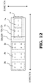
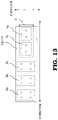
- FIG. 11 to FIG. 14 are schematic diagrams showing a component configuration of a power conversion device according to Embodiment 2.
- FIG. 11 is a top view
- FIG. 12 to FIG. 14 are side views
- FIG. 12 and FIG. 13 are side views in which some busbars are excluded from busbars shown in FIG. 11 .
- FIG. 15 is a circuit diagram showing an equivalent circuit of the power conversion device shown in FIG. 11 to FIG. 14 . That is, FIG. 11 to FIG. 14 are schematic diagrams in which the components on the circuit shown in FIG. 15 are disposed.
- the power conversion device according to the present Embodiment 2 is a power conversion device in which the number of the DC capacitors is increased by one from the number in the power conversion device according to Embodiment 1, i.e., the number of the DC capacitors is three.
- the first switching element 1a and the second switching element 1b are the same components as those in Embodiment 1.
- the three DC capacitors, i.e., the first DC capacitor 2a, the second DC capacitor 2b, and a third DC capacitor 2c, are provided as DC capacitors.
- the first switching element 1a, the second switching element 1b, the first DC capacitor 2a, the second DC capacitor 2b, and the third DC capacitor 2c have respective positive terminals and respective negative terminals, and are disposed in a straight line in the X direction such that all of the positive terminals and the negative terminals are aligned on the same side.
- the first switching element 1a and the second switching element 1b are adjacent to each other, the first DC capacitor 2a, the second DC capacitor 2b, and the third DC capacitor 2c are disposed in this order, and the DC capacitor disposed farthest from the switching elements is defined as the first DC capacitor 2a.
- the midpoint busbar 10c makes bridge connection between the negative terminal Ea of the first switching element 1a and the positive terminal Cb of the second switching element 1b.
- the positive terminal Ca of the first switching element 1a and the positive terminal Pa of the first DC capacitor 2a are electrically connected to each other by the first positive-side busbar 11p
- the positive terminal Ca of the first switching element 1a and the positive terminal Pb of the second DC capacitor 2b are electrically connected to each other by the second positive-side busbar 12p
- the positive terminal Ca of the first switching element 1a and each of positive terminals Pc of the third DC capacitor 2c are electrically connected to each other by a third positive-side busbar 13p.
- the negative terminal Eb of the second switching element 1b and the negative terminal Na of the first DC capacitor 2a are electrically connected to each other by the first negative-side busbar 11n
- the negative terminal Eb of the second switching element 1b and the negative terminal Nb of the second DC capacitor 2b are electrically connected to each other by the second negative-side busbar 12n
- the negative terminal Eb of the second switching element 1b and each of negative terminals Nc of the third DC capacitor 2c are electrically connected to each other by a third negative-side busbar 13n.
- the second positive-side busbar 12p has the inductance adjustment portion 32p providing a bypass such that the length on the second positive-side busbar 12p between the positive terminal Ca of the first switching element 1a and the positive terminal Pb of the second DC capacitor 2b is longer than the straight distance between the positive terminal Ca of the first switching element 1a and the positive terminal Pb of the second DC capacitor 2b.
- the second positive-side busbar 12p having the inductance adjustment portion 32p is sometimes referred to also as the adjustment positive-side busbar 12p.
- the second negative-side busbar 12n has the inductance adjustment portion 32n providing a bypass such that the length on the second negative-side busbar 12n between the negative terminal Eb of the second switching element 1b and the negative terminal Nb of the second DC capacitor 2b is longer than the straight distance between the negative terminal Eb of the second switching element 1b and the negative terminal Nb of the second DC capacitor 2b.
- the second negative-side busbar 12n having the inductance adjustment portion 32n is sometimes referred to also as the adjustment negative-side busbar 12n.
- the third positive-side busbar 13p has an inductance adjustment portion 33p providing a bypass such that a length on the third positive-side busbar 13p between the positive terminal Ca of the first switching element 1a and the positive terminal Pc of the third DC capacitor 2c is longer than a straight distance between the positive terminal Ca of the first switching element 1a and the positive terminal Pc of the third DC capacitor 2c.
- the third positive-side busbar 13p having the inductance adjustment portion 33p is sometimes referred to also as an adjustment positive-side busbar 13p.
- the third negative-side busbar 13n has an inductance adjustment portion 33n providing a bypass such that a length on the third negative-side busbar 13n between the negative terminal Eb of the second switching element 1b and the negative terminal Nc of the third DC capacitor 2c is longer than a straight distance between the negative terminal Eb of the second switching element 1b and the negative terminal Nc of the third DC capacitor 2c.
- the third negative-side busbar 13n having the inductance adjustment portion 33n is sometimes referred to also as an adjustment negative-side busbar 13n.
- Each busbar is formed of, for example, a sheet-shaped metal.
- the positive-side busbar and the negative-side busbar which are connected to each DC capacitor, are disposed in a superposed manner such that sheet surfaces of the busbars face each other with an insulating member 40 (indicated by an alternate long and short dash line) being interposed therebetween.
- first positive-side busbar 11p and the first negative-side busbar 11n are disposed in a superposed manner with the insulating member 40 being interposed therebetween
- second positive-side busbar 12p and the second negative-side busbar 12n are disposed in a superposed manner with the insulating member 40 being interposed therebetween
- third positive-side busbar 13p and the third negative-side busbar 13n are disposed in a superposed manner with an insulating member 40 being interposed therebetween.
- the set of two busbars connected to the first DC capacitor 2a, the set of two busbars connected to the second DC capacitor 2b, and the set of two busbars connected to the third DC capacitor 2c may be disposed in a superposed manner with insulating members 40 being interposed between the respective sets.
- FIG. 11 shows a configuration in which the set of busbars connected to the first DC capacitor 2a disposed farthest is disposed between the set of busbars connected to the second DC capacitor 2b and the set of busbars connected to the third DC capacitor 2c.
- the order of disposing the busbars is not limited thereto.
- the set of busbars connected to the first DC capacitor 2a disposed farthest is disposed closest to the electrical components; the set of busbars connected to the second DC capacitor 2b is disposed next to the closest set; and the set of busbars connected to the third DC capacitor 2c is disposed on the outermost side.
- the second switching element 1b is disposed closer to the DC capacitors than the first switching element 1a is, the positions of the switching elements may be reversed. Furthermore, regarding the sequences of the positive terminals and the negative terminals of the respective switching elements, the sequence of the positive terminal and the negative terminal of one of the switching elements may be opposite to the sequence shown in FIG. 11 , or the sequences of the positive terminals and the negative terminals of both the first switching element 1a and the second switching element 1b may be opposite to the sequences shown in FIG. 11 . The same applies to the DC capacitors.
- the sequences of the positive terminals and the negative terminals of the DC capacitors are not limited to the sequences shown in FIG. 11 .
- the difference between the distance from the positive terminal Ca of the first switching element 1a to the positive terminal Pa of the first DC capacitor 2a and the distance from the positive terminal Ca of the first switching element 1a to the positive terminal Pb of the second DC capacitor 2b is preferably equal to the difference between the distance from the negative terminal Eb of the second switching element 1b to the negative terminal Na of the first DC capacitor 2a and the distance from the negative terminal Eb of the second switching element 1b to the negative terminal Nb of the second DC capacitor 2b.
- the sequence of the positive terminal and the negative terminal is preferably the same among the three DC capacitors.
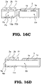
- FIG. 16A to FIG. 16H are perspective views showing the states of the busbars in an easily understandable manner.
- FIG. 16A shows a state where no busbar is present.
- FIG. 16B shows a state where the negative terminal Eb of the second switching element 1b and the negative terminal Nb of the second DC capacitor 2b are connected to each other by the second negative-side busbar 12n having the inductance adjustment portion 32n.
- FIG. 16C shows a state where the positive terminal Ca of the first switching element 1a and the positive terminal Pb of the second DC capacitor 2b are connected to each other by the second positive-side busbar 12p having the inductance adjustment portion 32p.
- FIG. 16D shows a state where the negative terminal Eb of the second switching element 1b and the negative terminal Na of the first DC capacitor 2a are connected to each other by the first negative-side busbar 11n.
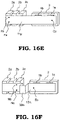
- FIG. 16E shows a state where the positive terminal Ca of the first switching element 1a and the positive terminal Pa of the first DC capacitor 2a are connected to each other by the first positive-side busbar 11p.
- FIG. 16F shows a state where the negative terminal Eb of the second switching element 1b and the negative terminal Nc of the third DC capacitor 2c are connected to each other by the third negative-side busbar 13n having the inductance adjustment portion 33n.
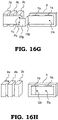
- FIG. 16G shows a state where the positive terminal Ca of the first switching element 1a and the positive terminal Pc of the third DC capacitor 2c are connected to each other by the third positive-side busbar 13p having the inductance adjustment portion 33p.
- FIG. 16H shows a state where the negative terminal Ea of the first switching element 1a and the positive terminal Cb of the second switching element 1b are connected to each other by the midpoint busbar 10c.
- Wiring inductances shown in the equivalent circuit in FIG. 15 are present between the terminals on the busbars. Specifically, the wiring inductance Lp1 is present on the first positive-side busbar 11p, the wiring inductance Ln1 is present on the first negative-side busbar 11n, the wiring inductance Lpb of the inductance adjustment portion 32p and the other wiring inductance Lp2 are present on the second positive-side busbar 12p, the wiring inductance Lnb of the inductance adjustment portion 32n and the other wiring inductance Ln2 are present on the second negative-side busbar 12n, a wiring inductance Lpc of the inductance adjustment portion 33p and another wiring inductance Lp3 are present on the third positive-side busbar 13p, and a wiring inductance Lnc of the inductance adjustment portion 33n and another wiring inductance Ln3 are present on the third negative-side busbar 13n.
- the lengths of the inductance adjustment portions are adjusted such that: the wiring inductances on the second positive-side busbar (adjustment positive-side busbar) 12p, i.e., the wiring inductance Lp2 and the wiring inductance Lpb of the inductance adjustment portion 32p, are equal to the wiring inductance Lp1 on the first positive-side busbar 11p; and the wiring inductances on the third positive-side busbar (adjustment positive-side busbar) 13p, i.e., the wiring inductance Lp3 and the wiring inductance Lpc of the inductance adjustment portion 33p, are equal to the wiring inductance Lp1 on the first positive-side busbar 11p.
- the lengths of the inductance adjustment portions are adjusted such that: the wiring inductances on the second negative-side busbar (adjustment negative-side busbar) 12n, i.e., the wiring inductance Ln2 and the wiring inductance Lnb of the inductance adjustment portion 32n, are equal to the wiring inductance Ln1 on the first negative-side busbar 11n; and the wiring inductances on the third negative-side busbar (adjustment negative-side busbar) 13n, i.e., the wiring inductance Ln3 and the wiring inductance Lnc of the inductance adjustment portion 33n, are equal to the wiring inductance Ln1 on the first negative-side busbar 11n.
- the lengths from the switching elements to the DC capacitors are adjusted by bending or curving the inductance adjustment portions, whereby variation in current among the DC capacitors can be eliminated.
- the above busbar configuration leads to presence of three busbars in which different currents flow through: a path between each switching element and the first DC capacitor 2a; a path between the switching element and the second DC capacitor 2b; and a path between the switching element and the third DC capacitor 2c. Consequently, the value of current flowing in each busbar is one third of the value in the conventional busbar configuration and, with the thickness dimension being kept unchanged from the conventional thickness dimension, heat generation from the busbar is less likely to occur, whereby the output current of the power conversion device can be increased.
- the thickness dimension of each busbar can be set to one third of the conventional thickness dimension.
- the dimension in the Y direction of each cell converter 60 does not increase even if the number of the DC capacitors that are in parallel is increased.
- increase in the dimension in the Y direction of each cell converter housing 61 can be avoided.
- the number of the cell converters 60 that can be accommodated in the cell converter housing 61 does not have to be decreased.
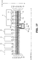
- FIG. 17 is a schematic diagram showing a component configuration of a power conversion device according to Embodiment 3.
- the power conversion device according to the present Embodiment 3 is a power conversion device in which the number of the DC capacitors is further increased by one from the number in the power conversion device according to Embodiment 2, i.e., the number of the DC capacitors is four.
- the first switching element 1a and the second switching element 1b are the same components as those in Embodiment 1 and Embodiment 2.
- DC capacitors i.e., the first DC capacitor 2a, the second DC capacitor 2b, the third DC capacitor 2c, and a fourth DC capacitor 2d
- the first switching element 1a, the second switching element 1b, the first DC capacitor 2a, the second DC capacitor 2b, the third DC capacitor 2c, and the fourth DC capacitor 2d have respective positive terminals and respective negative terminals, and are disposed in a straight line in the X direction such that all of the positive terminals and the negative terminals are aligned on the same side.
- the first switching element 1a and the second switching element 1b are adjacent to each other, the first DC capacitor 2a, the second DC capacitor 2b, the third DC capacitor 2c, and the fourth DC capacitor 2d are disposed in this order, and the DC capacitor disposed farthest from the switching elements is defined as the first DC capacitor 2a.
- the midpoint busbar 10c makes bridge connection between the negative terminal Ea of the first switching element 1a and the positive terminal Cb of the second switching element 1b.
- the positive terminal Ca of the first switching element 1a and the positive terminal Pa of the first DC capacitor 2a are electrically connected to each other by the first positive-side busbar 11p
- the positive terminal Ca of the first switching element 1a and the positive terminal Pb of the second DC capacitor 2b are electrically connected to each other by the second positive-side busbar 12p
- the positive terminal Ca of the first switching element 1a and the positive terminal Pc of the third DC capacitor 2c are electrically connected to each other by the third positive-side busbar 13p
- the positive terminal Ca of the first switching element 1a and each of positive terminals Pd of the fourth DC capacitor 2d are electrically connected to each other by a fourth positive-side busbar 14p.
- the negative terminal Eb of the second switching element 1b and the negative terminal Na of the first DC capacitor 2a are electrically connected to each other by the first negative-side busbar 11n
- the negative terminal Eb of the second switching element 1b and the negative terminal Nb of the second DC capacitor 2b are electrically connected to each other by the second negative-side busbar 12n
- the negative terminal Eb of the second switching element 1b and the negative terminal Nc of the third DC capacitor 2c are electrically connected to each other by the third negative-side busbar 13n
- the negative terminal Eb of the second switching element 1b and each of negative terminals Nd of the fourth DC capacitor 2d are electrically connected to each other by a fourth negative-side busbar 14n.
- the second positive-side busbar 12p has the inductance adjustment portion 32p providing a bypass such that the length on the second positive-side busbar 12p between the positive terminal Ca of the first switching element 1a and the positive terminal Pb of the second DC capacitor 2b is longer than the straight distance between the positive terminal Ca of the first switching element 1a and the positive terminal Pb of the second DC capacitor 2b.
- the second positive-side busbar 12p having the inductance adjustment portion 32p is sometimes referred to also as the adjustment positive-side busbar 12p.
- the second negative-side busbar 12n has the inductance adjustment portion 32n providing a bypass such that the length on the second negative-side busbar 12n between the negative terminal Eb of the second switching element 1b and the negative terminal Nb of the second DC capacitor 2b is longer than the straight distance between the negative terminal Eb of the second switching element 1b and the negative terminal Nb of the second DC capacitor 2b.
- the second negative-side busbar 12n having the inductance adjustment portion 32n is sometimes referred to also as the adjustment negative-side busbar 12n.
- the third positive-side busbar 13p has the inductance adjustment portion 33p providing a bypass such that the length on the third positive-side busbar 13p between the positive terminal Ca of the first switching element 1a and the positive terminal Pc of the third DC capacitor 2c is longer than the straight distance between the positive terminal Ca of the first switching element 1a and the positive terminal Pc of the third DC capacitor 2c.
- the third positive-side busbar 13p having the inductance adjustment portion 33p is sometimes referred to also as the adjustment positive-side busbar 13p.
- the third negative-side busbar 13n has the inductance adjustment portion 33n providing a bypass such that the length on the third negative-side busbar 13n between the negative terminal Eb of the second switching element 1b and the negative terminal Nc of the third DC capacitor 2c is longer than the straight distance between the negative terminal Eb of the second switching element 1b and the negative terminal Nc of the third DC capacitor 2c.
- the third negative-side busbar 13n having the inductance adjustment portion 33n is sometimes referred to also as the adjustment negative-side busbar 13n.
- the fourth positive-side busbar 14p has an inductance adjustment portion 34p providing a bypass such that a length on the fourth positive-side busbar 14p between the positive terminal Ca of the first switching element 1a and the positive terminal Pd of the fourth DC capacitor 2d is longer than a straight distance between the positive terminal Ca of the first switching element 1a and the positive terminal Pd of the fourth DC capacitor 2d.
- the fourth positive-side busbar 14p having the inductance adjustment portion 34p is sometimes referred to also as an adjustment positive-side busbar 14p.
- the fourth negative-side busbar 14n has an inductance adjustment portion 34n providing a bypass such that a length on the fourth negative-side busbar 14n between the negative terminal Eb of the second switching element 1b and the negative terminal Nd of the fourth DC capacitor 2d is longer than a straight distance between the negative terminal Eb of the second switching element 1b and the negative terminal Nd of the fourth DC capacitor 2d.
- the fourth negative-side busbar 14n having the inductance adjustment portion 34n is sometimes referred to also as an adjustment negative-side busbar 14n.
- the lengths of the inductance adjustment portions are adjusted such that inductances, on each adjustment positive-side busbar, between the positive terminal Ca of the first switching element 1a and the positive terminal Pa of the corresponding DC capacitor are equal to the inductance between the positive terminal Ca of the first switching element 1a and the positive terminal of the first DC capacitor 2a.
- the lengths of the inductance adjustment portions are adjusted such that inductances, on each adjustment negative-side busbar, between the negative terminal Eb of the second switching element 1b and the negative terminal of the corresponding DC capacitor are equal to the inductance between the negative terminal Eb of the second switching element 1b and the negative terminal Na of the first DC capacitor 2a.
- the lengths from the switching elements to the DC capacitors are adjusted by bending or curving the inductance adjustment portions, whereby variation in current among the DC capacitors can be eliminated.
- the above busbar configuration leads to presence of four busbars in which different currents flow through: a path between each switching element and the first DC capacitor 2a; a path between the switching element and the second DC capacitor 2b; a path between the switching element and the third DC capacitor 2c; and a path between the switching element and the fourth DC capacitor 2d. Consequently, the value of current flowing in each busbar is one fourth of the value in the conventional busbar configuration and, with the thickness dimension being kept unchanged from the conventional thickness dimension, heat generation from the busbar is less likely to occur, whereby the output current of the power conversion device can be increased.
- the thickness dimension of each busbar can be set to one fourth of the conventional thickness dimension.
- the dimension in the Y direction of each cell converter 60 does not increase even if the number of the DC capacitors that are in parallel is increased. Thus, increase in the dimension in the Y direction of each cell converter housing 61 can be avoided.
- the number of the cell converters 60 that can be accommodated in the cell converter housing 61 does not have to be decreased. Since the number of the cell converters 60 in each one of the valves is not decreased, no valves need to be additionally provided in the height direction so that the height of the valve tower 67 does not increase, either. Thus, the distance between the valve tower 67 and the ceiling portion of the valve hall 68 does not narrow, either. Therefore, even if the rated output current of a single cell converter 60 is increased, no problem arises in that the output of the entire power conversion device is decreased.
- the power conversion device is a power conversion device in which: a negative terminal of a first switching element and a positive terminal of a second switching element are connected to each other; and each of a plurality of DC capacitors is connected in parallel between a positive terminal of the first switching element and a negative terminal of the second switching element.
- the first switching element, the second switching element, and the plurality of DC capacitors are disposed in this order or the second switching element, the first switching element, and the plurality of DC capacitors are disposed in this order, such that all of positive terminals and negative terminals are aligned on a same side.
- Busbars connecting the switching elements and a DC capacitor other than the DC capacitor disposed farthest from the switching elements to each other, are provided with inductance adjustment portions for adjusting the lengths of the said busbars to adjust inductances.
- the inductances on the busbars connecting the switching elements and the respective DC capacitors to each other can be set to be equal to one another, whereby variation in current among the DC capacitors can be eliminated. Further, with the thickness dimension being kept unchanged from the conventional thickness dimension, heat generation from the busbars is less likely to occur than in the conventional busbar configuration, and the output current of the power conversion device can be set to be higher than in the conventional busbar configuration.
- the dimension of each busbar can be set to be smaller than the conventional thickness.
Landscapes
- Engineering & Computer Science (AREA)
- Power Engineering (AREA)
- Inverter Devices (AREA)
Abstract
Description
- The present invention relates to a power conversion device.
- A modular multilevel converter (MMC) is of a circuit type in which output terminals of cell converters each composed of a DC capacitor and a switching element capable of being controlled to be turned on/off such as an IGBT are connected in series so that a high voltage higher than a withstanding voltage of the switching element can be outputted. The MMC is expected to be applied to DC power transmission systems (HVDCs), reactive power compensation devices (STATCOMs), and the like. According to
Patent Document 1, an MMC is formed by connecting a plurality of cell converters in series (cascade). Each cell converter is composed of: a main circuit composed of a switching element and a DC capacitor; and an external terminal for cascade connection to another one of the cell converters. An external conductor is used for bridge connection between the switching elements. - Meanwhile, increase of a rated current of the cell converter requires both increase of a rated current of the switching element and increase of a capacitance of the DC capacitor. The easiest way to increase the capacitance of the DC capacitor is to increase the number of DC capacitors that are in parallel (see, for example, Patent Document 2).
-
- Patent Document 1: Japanese Laid-open Patent Publication (translation of PCT application)
JP 2011- 503 852 A - Patent Document 2: Japanese Laid-Open Patent Publication
JP 2004- 289 955 A - In
Patent Document 2, DC capacitors that are used in parallel are mounted at the same distance from a switching element. Thus, wiring inductances on busbars connecting the switching element and the respective DC capacitors are basically equal to one another between the switching element and each DC capacitor. Therefore, the magnitudes of currents flowing from the switching element to the respective DC capacitors are also basically equal to one another. - However, the configuration in
Patent Document 2 has the following drawback. That is, if DC capacitors are additionally provided from the state inFIG. 3 to the state inFIG. 7 inPatent Document 2, the width of a cell converter is increased in an arrangement configuration of a power conversion device intended for HVDCs. Considering this, the number of the cell converters that can be accommodated in a cell converter accommodation frame has to be decreased, or the horizontal dimension of the cell converter accommodation frame has to be increased. - The present invention has been made to solve the above drawback, and an object of the present invention is to obtain a power conversion device in which the magnitudes of currents flowing to respective DC capacitors are set to be equal to one another; and the width of a cell converter does not increase even if the number of the DC capacitors that are used in parallel is increased.
- A power conversion device according to the present invention includes: a first switching element and a second switching element each having a positive terminal and a negative terminal; and a plurality of DC capacitors each having a positive terminal and a negative terminal. The negative terminal of the first switching element and the positive terminal of the second switching element are connected to each other. Each of the plurality of DC capacitors is connected in parallel between the positive terminal of the first switching element and the negative terminal of the second switching element.
- The first switching element, the second switching element, and the plurality of DC capacitors are disposed in this order or the second switching element, the first switching element, and the plurality of DC capacitors are disposed in this order, such that all of the positive terminals and the negative terminals are aligned on a same side.
- A plurality of positive-side busbars are provided, the number of the positive-side busbars being equal to the number of the DC capacitors, each positive-side busbar connecting the positive terminal of the first switching element and the positive terminal of a corresponding one of the plurality of DC capacitors to each other.
- A plurality of negative-side busbars are provided, the number of the negative-side busbars being equal to the number of the DC capacitors, each negative-side busbar connecting the negative terminal of the second switching element and the negative terminal of a corresponding one of the plurality of DC capacitors to each other.
- An adjustment positive-side busbar which is a positive-side busbar among the plurality of positive-side busbars other than the positive-side busbar connected to the DC capacitor farthest from the first switching element, has an inductance adjustment portion providing a bypass such that a length on the adjustment positive-side busbar between the positive terminal of the first switching element and the positive terminal of the DC capacitor to which the adjustment positive-side busbar is connected, is longer than a straight distance between the positive terminal of the first switching element and the positive terminal of the DC capacitor to which the adjustment positive-side busbar is connected.
- An adjustment negative-side busbar which is a negative-side busbar among the plurality of negative-side busbars other than the negative-side busbar connected to the DC capacitor farthest from the second switching element, has an inductance adjustment portion providing a bypass such that a length on the adjustment negative-side busbar between the negative terminal of the second switching element and the negative terminal of the DC capacitor to which the adjustment negative-side busbar is connected, is longer than a straight distance between the negative terminal of the second switching element and the negative terminal of the DC capacitor to which the adjustment negative-side busbar is connected.
- The power conversion device according to the present invention leads to obtainment of a power conversion device in which: the magnitudes of currents flowing to respective DC capacitors are set to be equal to one another; and the width of a cell converter does not increase even if the number of the DC capacitors that are used in parallel is increased.
-
-
FIG. 1 is a first schematic diagram showing a configuration of a power conversion device according toEmbodiment 1. -
FIG. 2 is a second schematic diagram showing the configuration of the power conversion device according toEmbodiment 1. -
FIG. 3 is a third schematic diagram showing the configuration of the power conversion device according toEmbodiment 1. -
FIG. 4 is a circuit diagram showing an equivalent circuit of the power conversion device according toEmbodiment 1. -
FIG. 5A is a first diagram for explaining a busbar connection state in the power conversion device according toEmbodiment 1. -
FIG. 5B is a second diagram for explaining the busbar connection state in the power conversion device according toEmbodiment 1. -
FIG. 5C is a third diagram for explaining the busbar connection state in the power conversion device according toEmbodiment 1. -
FIG. 5D is a fourth diagram for explaining the busbar connection state in the power conversion device according toEmbodiment 1. -
FIG. 5E is a fifth diagram for explaining the busbar connection state in the power conversion device according toEmbodiment 1. -
FIG. 5F is a sixth diagram for explaining the busbar connection state in the power conversion device according toEmbodiment 1. -
FIG. 6 is a schematic diagram showing another configuration of the power conversion device according toEmbodiment 1. -
FIG. 7 is a schematic diagram showing still another configuration of the power conversion device according toEmbodiment 1. -
FIG. 8 is a schematic diagram showing a configuration in a case where the power conversion device according toEmbodiment 1 is configured as a cell converter. -
FIG. 9 is a circuit diagram showing an equivalent circuit in the case where the power conversion device according toEmbodiment 1 is configured as the cell converter. -
FIG. 10 is a schematic diagram showing a configuration of a power conversion device intended for HVDCs, in which the power conversion device according toEmbodiment 1 is used as the cell converter. -
FIG. 11 is a first schematic diagram showing a configuration of a power conversion device according toEmbodiment 2. -
FIG. 12 is a second schematic diagram showing the configuration of the power conversion device according toEmbodiment 2. -
FIG. 13 is a third schematic diagram showing the configuration of the power conversion device according toEmbodiment 2. -
FIG. 14 is a fourth schematic diagram showing the configuration of the power conversion device according toEmbodiment 2. -
FIG. 15 is a circuit diagram showing an equivalent circuit of the power conversion device according toEmbodiment 2. -
FIG. 16A is a first diagram for explaining a busbar connection state in the power conversion device according toEmbodiment 2. -
FIG. 16B is a second diagram for explaining the busbar connection state in the power conversion device according toEmbodiment 2. -
FIG. 16C is a third diagram for explaining the busbar connection state in the power conversion device according toEmbodiment 2. -
FIG. 16D is a fourth diagram for explaining the busbar connection state in the power conversion device according toEmbodiment 2. -
FIG. 16E is a fifth diagram for explaining the busbar connection state in the power conversion device according toEmbodiment 2. -
FIG. 16F is a sixth diagram for explaining the busbar connection state in the power conversion device according toEmbodiment 2. -
FIG. 16G is a seventh diagram for explaining the busbar connection state in the power conversion device according toEmbodiment 2. -
FIG. 16H is an eighth diagram for explaining the busbar connection state in the power conversion device according toEmbodiment 2. -
FIG. 17 is a schematic diagram showing a configuration of a power conversion device according toEmbodiment 3. -
FIG. 1 to FIG. 3 are schematic diagrams showing a component configuration of a power conversion device according toEmbodiment 1.FIG. 1 is a top view, andFIG. 2 andFIG. 3 are side views.FIG. 2 is a side view in which some busbars are excluded from busbars shown in the top view inFIG. 1 .FIG. 4 is a circuit diagram showing an equivalent circuit of the power conversion device shown inFIG. 1 to FIG. 3 . That is,FIG. 1 to FIG. 3 are schematic diagrams in which components on the circuit shown inFIG. 4 are disposed. - The power conversion device according to
Embodiment 1 is a power conversion device including: afirst switching element 1a in which a first switch and a first diode connected in antiparallel to the first switch are mounted; asecond switching element 1b in which a second switch and a second diode connected in antiparallel to the second switch are mounted; afirst DC capacitor 2a; asecond DC capacitor 2b; and acooler 3 which is mounted with thefirst switching element 1a and thesecond switching element 1b and which cools the switching elements. - The
first switching element 1a and thesecond switching element 1b are mounted on a flat surface portion of thecooler 3 by means of fixation members such as screws so as to be parallel to the shape of thecooler 3 in an X direction. Here, thefirst switching element 1a, thesecond switching element 1b, thefirst DC capacitor 2a, and thesecond DC capacitor 2b have respective positive terminals and respective negative terminals, and are disposed to be aligned in the X direction such that all of the positive terminals and the negative terminals are on a same side. Thefirst switching element 1a and thesecond switching element 1b are disposed to be adjacent to each other, and thefirst DC capacitor 2a and thesecond DC capacitor 2b are disposed to be adjacent to each other. The DC capacitor disposed farther from the switching elements is defined as thefirst DC capacitor 2a. - These electrical components are electrically connected to each other by busbars in order to form the circuit in
FIG. 4 . Amidpoint busbar 10c makes bridge connection between a negative terminal Ea of thefirst switching element 1a and a positive terminal Cb of thesecond switching element 1b. A positive terminal Ca of thefirst switching element 1a and a positive terminal Pa of thefirst DC capacitor 2a are electrically connected to each other by a first positive-side busbar 11p, and the positive terminal Ca of thefirst switching element 1a and a positive terminal Pb of thesecond DC capacitor 2b are electrically connected to each other by a second positive-side busbar 12p. - A negative terminal Eb of the
second switching element 1b and a negative terminal Na of thefirst DC capacitor 2a are electrically connected to each other by a first negative-side busbar 11n, and the negative terminal Eb of thesecond switching element 1b and a negative terminal Nb of thesecond DC capacitor 2b are electrically connected to each other by a second negative-side busbar 12n. - Here, the second positive-
side busbar 12p has aninductance adjustment portion 32p providing a bypass such that a length on the second positive-side busbar 12p between the positive terminal Ca of thefirst switching element 1a and the positive terminal Pb of thesecond DC capacitor 2b is longer than a straight distance between the positive terminal Ca of thefirst switching element 1a and the positive terminal Pb of thesecond DC capacitor 2b. - The second positive-
side busbar 12p having theinductance adjustment portion 32p is sometimes referred to also as an adjustment positive-side busbar 12p. Further, the second negative-side busbar 12n has aninductance adjustment portion 32n providing a bypass such that a length on the second negative-side busbar 12n between the negative terminal Eb of thesecond switching element 1b and the negative terminal Nb of thesecond DC capacitor 2b is longer than a straight distance between the negative terminal Eb of thesecond switching element 1b and the negative terminal Nb of thesecond DC capacitor 2b. The second negative-side busbar 12n having theinductance adjustment portion 32n is sometimes referred to also as an adjustment negative-side busbar 12n. - Each busbar is formed of, for example, a sheet-shaped metal. The positive-side busbar and the negative-side busbar which are connected to each DC capacitor, are disposed in a superposed manner such that sheet surfaces of the busbars face each other with an insulating member 40 (indicated by an alternate long and short dash line) being interposed therebetween. Specifically, the first positive-
side busbar 11p and the first negative-side busbar 11n are disposed in a superposed manner with an insulatingmember 40 being interposed therebetween, and the second positive-side busbar 12p and the second negative-side busbar 12n are disposed in a superposed manner with an insulatingmember 40 being interposed therebetween. - Further, the set of two busbars connected to the
first DC capacitor 2a and the set of two busbars connected to thesecond DC capacitor 2b may be disposed in a superposed manner with an insulatingmember 40 being interposed between the sets. Although, inFIG. 1 , the first negative-side busbar 11n is disposed closer to the switching elements and the DC capacitors than the first positive-side busbar 11p is, the positions of these busbars may be reversed. Likewise, although the second negative-side busbar 12n is disposed closer to the switching elements and the DC capacitors than the second positive-side busbar 12p is, the positions of these busbars may be reversed. -
FIG. 5A to FIG. 5F are perspective views showing the states of the busbars in an easily understandable manner.FIG. 5A shows a state where no busbar is present.FIG. 5B shows a state where the negative terminal Eb of thesecond switching element 1b and the negative terminal Na of thefirst DC capacitor 2a are connected to each other by the first negative-side busbar 11n.FIG. 5C shows a state where the positive terminal Ca of thefirst switching element 1a and the positive terminal Pa of thefirst DC capacitor 2a are connected to each other by the first positive-side busbar 11p. -
FIG. 5D shows a state where the negative terminal Eb of thesecond switching element 1b and the negative terminal Nb of thesecond DC capacitor 2b are connected to each other by the second negative-side busbar 12n having theinductance adjustment portion 32n.FIG. 5E shows a state where the positive terminal Ca of thefirst switching element 1a and the positive terminal Pb of thesecond DC capacitor 2b are connected to each other by the second positive-side busbar 12p having theinductance adjustment portion 32p.FIG. 5F shows a state where the negative terminal Ea of thefirst switching element 1a and the positive terminal Cb of thesecond switching element 1b are connected to each other by themidpoint busbar 10c. -
FIG. 6 is a schematic diagram showing another component configuration of the power conversion device according toEmbodiment 1. The sequences of the positive terminals and the negative terminals of the DC capacitors are not limited to the sequences inFIG. 1 , and the positive terminals may be located farther from the switching elements as shown inFIG. 6 . - That is, either of the positive terminals and the negative terminals may be located farther from the switching elements. However, the sequence of the positive terminal and the negative terminal is preferably the same between the DC capacitors. Specifically, the sequence of the positive terminal and the negative terminal is preferably the same between the
first DC capacitor 2a and thesecond DC capacitor 2b such that the difference between the distance from the positive terminal Ca of thefirst switching element 1a to the positive terminal Pa of thefirst DC capacitor 2a and the distance from the positive terminal Ca of thefirst switching element 1a to the positive terminal Pb of thesecond DC capacitor 2b is equal to the difference between the distance from the negative terminal Eb of thesecond switching element 1b to the negative terminal Na of thefirst DC capacitor 2a and the distance from the negative terminal Eb of thesecond switching element 1b to the negative terminal Nb of thesecond DC capacitor 2b. -
FIG. 7 is a schematic diagram showing still another component configuration of the power conversion device according toEmbodiment 1. As shown inFIG. 7 , either of thefirst switching element 1a and thesecond switching element 1b may be disposed closer to the DC capacitors as long as the negative terminal Ea of thefirst switching element 1a and the positive terminal Cb of thesecond switching element 1b are connected to each other. Further, regarding the switching elements, the sequence of the positive terminal and the negative terminal may be reversed between the switching elements. - As described above, the sequence of the
first switching element 1a and thesecond switching element 1b and the sequence of the positive terminal and the negative terminal thereof, are not limited in terms of order. Meanwhile, the sequence of the positive terminal and the negative terminal is preferably the same between thefirst DC capacitor 2a and thesecond DC capacitor 2b. - Wiring inductances shown in the equivalent circuit in
FIG. 4 are present between the terminals on the busbars. Specifically, a wiring inductance Lp1 is present on the first positive-side busbar 11p, a wiring inductance Ln1 is present on the first negative-side busbar 11n, a wiring inductance Lpb of theinductance adjustment portion 32p and another wiring inductance Lp2 are present on the second positive-side busbar 12p, and a wiring inductance Lnb of theinductance adjustment portion 32n and another wiring inductance Ln2 are present on the second negative-side busbar 12n. - Regarding the above wiring inductances between the switching elements and the DC capacitors based on the arrangement of the switching elements and the DC capacitors, the lengths of the inductance adjustment portions are adjusted such that: the wiring inductances on the second positive-side busbar (adjustment positive-side busbar) 12p, i.e., the wiring inductance Lp2 and the wiring inductance Lpb of the
inductance adjustment portion 32p, are equal to the wiring inductance Lp1 on the first positive-side busbar; and the wiring inductances on the second negative-side busbar (adjustment negative-side busbar) 12n, i.e., the wiring inductance Ln2 and the wiring inductance Lnb of theinductance adjustment portion 32n, are equal to the wiring inductance Ln1 on the first negative-side busbar. That is, in theinductance adjustment portion 32p and theinductance adjustment portion 32n, the lengths from the switching elements to the DC capacitors are adjusted by bending or curving the inductance adjustment portions, whereby variation in current between the DC capacitors can be eliminated. - Further, the above busbar configuration leads to presence of two busbars in which different currents flow through: a path between each switching element and the
first DC capacitor 2a; and a path between the switching element and thesecond DC capacitor 2b. Consequently, the value of current flowing in each busbar is half the value in a conventional busbar configuration and, with a thickness dimension being equal to a conventional thickness dimension, heat generated from the busbar at the same level of current is lower than in the conventional busbar configuration, whereby output current of the power conversion device can be increased. - Meanwhile, if the same level of heat generation as that in the conventional busbar configuration can be performed, the thickness dimension of each busbar can be set to half the conventional thickness dimension. Thus, machining work such as bending of the busbars becomes easy, and the weight of each single busbar is decreased, whereby assembling work becomes easy.
-
FIG. 8 is a schematic diagram showing a configuration in a case where the power conversion device according toEmbodiment 1 is configured as acell converter 60.FIG. 9 is a diagram showing an equivalent circuit of thecell converter 60.FIG. 8 andFIG. 9 are different fromFIG. 1 andFIG. 4 in that: an external terminal X1 is provided at a position, on themidpoint busbar 10c, that is an end portion of thecell converter 60; and an external terminal X2 is provided at a position that is an end portion of thecell converter 60 and at which the first negative-side busbar 11n and the second negative-side busbar 12n are connected to each other. The external terminal X1 and the external terminal X2 are located on a front side of thecell converter 60. -
FIG. 10 is a schematic diagram showing an arrangement configuration of a general power conversion device intended for HVDCs and shows a connection configuration in which a plurality ofcell converters 60 each of which is thecell converter 60 shown inFIG. 8 are used. The plurality ofcell converters 60 are aligned in a horizontal Y direction and accommodated in onecell converter housing 61. -
FIG. 10 shows an example in which fourcell converters 60 are accommodated in onecell converter housing 61. As described above, eachcell converter 60 has the external terminal X1 and the external terminal X2. The external terminal X1 of thecell converter 60 and the external terminal X2 of anothercell converter 60 adjacent thereto are connected to each other via an inter-cell-converter connection conductor 62, and the external terminal X2 of theother cell converter 60 and the external terminal X1 of still anothercell converter 60 adjacent thereto are connected to each other via an inter-cell-converter connection conductor 62, whereby the plurality ofcell converters 60 are connected in series. - This component in which the plurality of
cell converters 60 accommodated in thecell converter housing 61 are connected in series, i.e., connected in cascade, is referred to as avalve 63. In order to increase output voltage, a plurality of thevalves 63 are stacked in the vertical direction (height direction, Z direction) and connected to each other via aninter-valve connection conductor 64 so that the number of thecell converters 60 that are connected in series can be set to be further larger than in a configuration provided with only one valve. - Insulating
structures 65 are disposed between thevalves 63 so as not to cause an electrical short-circuit between the highest potential among those of thecell converters 60 connected in cascade and another reference potential, whereby the distances to theother valve 63 and areference potential 66 are ensured. A structure composed of the plurality ofvalves 63 and the plurality of insulatingstructures 65 is referred to as avalve tower 67. Thevalve tower 67 is accommodated in avalve hall 68 so as not to be directly influenced by external environments, e.g., rain and temperature. - In the above configuration, the dimension in the Y direction of each
cell converter 60 does not increase even if the number of the DC capacitors that are in parallel is increased as described later inEmbodiment 2 andEmbodiment 3. Thus, increase in the dimension in the Y direction of eachcell converter housing 61 can be avoided. Meanwhile, even if a restriction is imposed on the dimension in the Y direction of thecell converter housing 61, the number of thecell converters 60 that can be accommodated in thecell converter housing 61 does not have to be decreased. - Since the number of the
cell converters 60 in each one of thevalves 63 is not decreased, novalves 63 need to be additionally provided in the vertical direction so that the height of thevalve tower 67 does not increase, either. Thus, the distance between thevalve tower 67 and a ceiling portion of thevalve hall 68 does not narrow, either. Therefore, even if the rated output current of asingle cell converter 60 is increased, no problem arises in that the output of the entire power conversion device is decreased. -
FIG. 11 to FIG. 14 are schematic diagrams showing a component configuration of a power conversion device according toEmbodiment 2.FIG. 11 is a top view,FIG. 12 to FIG. 14 are side views, andFIG. 12 andFIG. 13 are side views in which some busbars are excluded from busbars shown inFIG. 11 .FIG. 15 is a circuit diagram showing an equivalent circuit of the power conversion device shown inFIG. 11 to FIG. 14 . That is,FIG. 11 to FIG. 14 are schematic diagrams in which the components on the circuit shown inFIG. 15 are disposed. - The power conversion device according to the
present Embodiment 2 is a power conversion device in which the number of the DC capacitors is increased by one from the number in the power conversion device according toEmbodiment 1, i.e., the number of the DC capacitors is three. Thefirst switching element 1a and thesecond switching element 1b are the same components as those inEmbodiment 1. The three DC capacitors, i.e., thefirst DC capacitor 2a, thesecond DC capacitor 2b, and athird DC capacitor 2c, are provided as DC capacitors. - Here, the
first switching element 1a, thesecond switching element 1b, thefirst DC capacitor 2a, thesecond DC capacitor 2b, and thethird DC capacitor 2c have respective positive terminals and respective negative terminals, and are disposed in a straight line in the X direction such that all of the positive terminals and the negative terminals are aligned on the same side. Thefirst switching element 1a and thesecond switching element 1b are adjacent to each other, thefirst DC capacitor 2a, thesecond DC capacitor 2b, and thethird DC capacitor 2c are disposed in this order, and the DC capacitor disposed farthest from the switching elements is defined as thefirst DC capacitor 2a. - These electrical components are electrically connected to each other by busbars in order to form the circuit in
FIG. 15 . Themidpoint busbar 10c makes bridge connection between the negative terminal Ea of thefirst switching element 1a and the positive terminal Cb of thesecond switching element 1b. The positive terminal Ca of thefirst switching element 1a and the positive terminal Pa of thefirst DC capacitor 2a are electrically connected to each other by the first positive-side busbar 11p, the positive terminal Ca of thefirst switching element 1a and the positive terminal Pb of thesecond DC capacitor 2b are electrically connected to each other by the second positive-side busbar 12p, and the positive terminal Ca of thefirst switching element 1a and each of positive terminals Pc of thethird DC capacitor 2c are electrically connected to each other by a third positive-side busbar 13p. - The negative terminal Eb of the
second switching element 1b and the negative terminal Na of thefirst DC capacitor 2a are electrically connected to each other by the first negative-side busbar 11n, the negative terminal Eb of thesecond switching element 1b and the negative terminal Nb of thesecond DC capacitor 2b are electrically connected to each other by the second negative-side busbar 12n, and the negative terminal Eb of thesecond switching element 1b and each of negative terminals Nc of thethird DC capacitor 2c are electrically connected to each other by a third negative-side busbar 13n. - Here, the second positive-
side busbar 12p has theinductance adjustment portion 32p providing a bypass such that the length on the second positive-side busbar 12p between the positive terminal Ca of thefirst switching element 1a and the positive terminal Pb of thesecond DC capacitor 2b is longer than the straight distance between the positive terminal Ca of thefirst switching element 1a and the positive terminal Pb of thesecond DC capacitor 2b. The second positive-side busbar 12p having theinductance adjustment portion 32p is sometimes referred to also as the adjustment positive-side busbar 12p. - Further, the second negative-
side busbar 12n has theinductance adjustment portion 32n providing a bypass such that the length on the second negative-side busbar 12n between the negative terminal Eb of thesecond switching element 1b and the negative terminal Nb of thesecond DC capacitor 2b is longer than the straight distance between the negative terminal Eb of thesecond switching element 1b and the negative terminal Nb of thesecond DC capacitor 2b. The second negative-side busbar 12n having theinductance adjustment portion 32n is sometimes referred to also as the adjustment negative-side busbar 12n. - Likewise, the third positive-
side busbar 13p has aninductance adjustment portion 33p providing a bypass such that a length on the third positive-side busbar 13p between the positive terminal Ca of thefirst switching element 1a and the positive terminal Pc of thethird DC capacitor 2c is longer than a straight distance between the positive terminal Ca of thefirst switching element 1a and the positive terminal Pc of thethird DC capacitor 2c. The third positive-side busbar 13p having theinductance adjustment portion 33p is sometimes referred to also as an adjustment positive-side busbar 13p. - Further, the third negative-
side busbar 13n has aninductance adjustment portion 33n providing a bypass such that a length on the third negative-side busbar 13n between the negative terminal Eb of thesecond switching element 1b and the negative terminal Nc of thethird DC capacitor 2c is longer than a straight distance between the negative terminal Eb of thesecond switching element 1b and the negative terminal Nc of thethird DC capacitor 2c. The third negative-side busbar 13n having theinductance adjustment portion 33n is sometimes referred to also as an adjustment negative-side busbar 13n. - Each busbar is formed of, for example, a sheet-shaped metal. The positive-side busbar and the negative-side busbar which are connected to each DC capacitor, are disposed in a superposed manner such that sheet surfaces of the busbars face each other with an insulating member 40 (indicated by an alternate long and short dash line) being interposed therebetween.
- Specifically, the first positive-
side busbar 11p and the first negative-side busbar 11n are disposed in a superposed manner with the insulatingmember 40 being interposed therebetween, the second positive-side busbar 12p and the second negative-side busbar 12n are disposed in a superposed manner with the insulatingmember 40 being interposed therebetween, and the third positive-side busbar 13p and the third negative-side busbar 13n are disposed in a superposed manner with an insulatingmember 40 being interposed therebetween. Further, the set of two busbars connected to thefirst DC capacitor 2a, the set of two busbars connected to thesecond DC capacitor 2b, and the set of two busbars connected to thethird DC capacitor 2c may be disposed in a superposed manner with insulatingmembers 40 being interposed between the respective sets. -
FIG. 11 shows a configuration in which the set of busbars connected to thefirst DC capacitor 2a disposed farthest is disposed between the set of busbars connected to thesecond DC capacitor 2b and the set of busbars connected to thethird DC capacitor 2c. However, the order of disposing the busbars is not limited thereto. For example, it is also possible that: the set of busbars connected to thefirst DC capacitor 2a disposed farthest is disposed closest to the electrical components; the set of busbars connected to thesecond DC capacitor 2b is disposed next to the closest set; and the set of busbars connected to thethird DC capacitor 2c is disposed on the outermost side. Alternatively, it is also possible to employ an arrangement in which the set of busbars connected to thesecond DC capacitor 2b and the set of busbars connected to thethird DC capacitor 2c inFIG. 11 are interchanged. - Further, although the
second switching element 1b is disposed closer to the DC capacitors than thefirst switching element 1a is, the positions of the switching elements may be reversed. Furthermore, regarding the sequences of the positive terminals and the negative terminals of the respective switching elements, the sequence of the positive terminal and the negative terminal of one of the switching elements may be opposite to the sequence shown inFIG. 11 , or the sequences of the positive terminals and the negative terminals of both thefirst switching element 1a and thesecond switching element 1b may be opposite to the sequences shown inFIG. 11 . The same applies to the DC capacitors. - That is, the sequences of the positive terminals and the negative terminals of the DC capacitors are not limited to the sequences shown in
FIG. 11 . However, the difference between the distance from the positive terminal Ca of thefirst switching element 1a to the positive terminal Pa of thefirst DC capacitor 2a and the distance from the positive terminal Ca of thefirst switching element 1a to the positive terminal Pb of thesecond DC capacitor 2b is preferably equal to the difference between the distance from the negative terminal Eb of thesecond switching element 1b to the negative terminal Na of thefirst DC capacitor 2a and the distance from the negative terminal Eb of thesecond switching element 1b to the negative terminal Nb of thesecond DC capacitor 2b. The same applies to thethird DC capacitor 2c, and the sequence of the positive terminal and the negative terminal is preferably the same among the three DC capacitors. -
FIG. 16A to FIG. 16H are perspective views showing the states of the busbars in an easily understandable manner.FIG. 16A shows a state where no busbar is present.FIG. 16B shows a state where the negative terminal Eb of thesecond switching element 1b and the negative terminal Nb of thesecond DC capacitor 2b are connected to each other by the second negative-side busbar 12n having theinductance adjustment portion 32n.FIG. 16C shows a state where the positive terminal Ca of thefirst switching element 1a and the positive terminal Pb of thesecond DC capacitor 2b are connected to each other by the second positive-side busbar 12p having theinductance adjustment portion 32p. -
FIG. 16D shows a state where the negative terminal Eb of thesecond switching element 1b and the negative terminal Na of thefirst DC capacitor 2a are connected to each other by the first negative-side busbar 11n.FIG. 16E shows a state where the positive terminal Ca of thefirst switching element 1a and the positive terminal Pa of thefirst DC capacitor 2a are connected to each other by the first positive-side busbar 11p.FIG. 16F shows a state where the negative terminal Eb of thesecond switching element 1b and the negative terminal Nc of thethird DC capacitor 2c are connected to each other by the third negative-side busbar 13n having theinductance adjustment portion 33n. -
FIG. 16G shows a state where the positive terminal Ca of thefirst switching element 1a and the positive terminal Pc of thethird DC capacitor 2c are connected to each other by the third positive-side busbar 13p having theinductance adjustment portion 33p.FIG. 16H shows a state where the negative terminal Ea of thefirst switching element 1a and the positive terminal Cb of thesecond switching element 1b are connected to each other by themidpoint busbar 10c. - Wiring inductances shown in the equivalent circuit in
FIG. 15 are present between the terminals on the busbars. Specifically, the wiring inductance Lp1 is present on the first positive-side busbar 11p, the wiring inductance Ln1 is present on the first negative-side busbar 11n, the wiring inductance Lpb of theinductance adjustment portion 32p and the other wiring inductance Lp2 are present on the second positive-side busbar 12p, the wiring inductance Lnb of theinductance adjustment portion 32n and the other wiring inductance Ln2 are present on the second negative-side busbar 12n, a wiring inductance Lpc of theinductance adjustment portion 33p and another wiring inductance Lp3 are present on the third positive-side busbar 13p, and a wiring inductance Lnc of theinductance adjustment portion 33n and another wiring inductance Ln3 are present on the third negative-side busbar 13n. - Regarding the above wiring inductances between the switching elements and the DC capacitors based on the arrangement of the switching elements and the DC capacitors, the lengths of the inductance adjustment portions are adjusted such that: the wiring inductances on the second positive-side busbar (adjustment positive-side busbar) 12p, i.e., the wiring inductance Lp2 and the wiring inductance Lpb of the
inductance adjustment portion 32p, are equal to the wiring inductance Lp1 on the first positive-side busbar 11p; and the wiring inductances on the third positive-side busbar (adjustment positive-side busbar) 13p, i.e., the wiring inductance Lp3 and the wiring inductance Lpc of theinductance adjustment portion 33p, are equal to the wiring inductance Lp1 on the first positive-side busbar 11p. - Likewise, the lengths of the inductance adjustment portions are adjusted such that: the wiring inductances on the second negative-side busbar (adjustment negative-side busbar) 12n, i.e., the wiring inductance Ln2 and the wiring inductance Lnb of the
inductance adjustment portion 32n, are equal to the wiring inductance Ln1 on the first negative-side busbar 11n; and the wiring inductances on the third negative-side busbar (adjustment negative-side busbar) 13n, i.e., the wiring inductance Ln3 and the wiring inductance Lnc of theinductance adjustment portion 33n, are equal to the wiring inductance Ln1 on the first negative-side busbar 11n. - That is, in the
inductance adjustment portion 32p and theinductance adjustment portion 32n, and theinductance adjustment portion 33p and theinductance adjustment portion 33n, the lengths from the switching elements to the DC capacitors are adjusted by bending or curving the inductance adjustment portions, whereby variation in current among the DC capacitors can be eliminated. - Further, the above busbar configuration leads to presence of three busbars in which different currents flow through: a path between each switching element and the
first DC capacitor 2a; a path between the switching element and thesecond DC capacitor 2b; and a path between the switching element and thethird DC capacitor 2c. Consequently, the value of current flowing in each busbar is one third of the value in the conventional busbar configuration and, with the thickness dimension being kept unchanged from the conventional thickness dimension, heat generation from the busbar is less likely to occur, whereby the output current of the power conversion device can be increased. - Meanwhile, if the same level of heat generation as that in the conventional busbar configuration can be performed, the thickness dimension of each busbar can be set to one third of the conventional thickness dimension. Thus, it is possible to solve the problems that machining work such as bending of the busbars becomes difficult, assembling work becomes difficult owing to increase in the weight of each single busbar, and other work becomes difficult.
- In the case where the power conversion device is applied to the power conversion device intended for HVDCs shown in
FIG. 10 , the dimension in the Y direction of eachcell converter 60 does not increase even if the number of the DC capacitors that are in parallel is increased. Thus, increase in the dimension in the Y direction of eachcell converter housing 61 can be avoided. Meanwhile, even if a restriction is imposed on the dimension in the Y direction of thecell converter housing 61, the number of thecell converters 60 that can be accommodated in thecell converter housing 61 does not have to be decreased. - Since the number of the
cell converters 60 in each one of the valves is not decreased, no valves need to be additionally provided in the height direction so that the height of thevalve tower 67 does not increase, either. Thus, the distance between thevalve tower 67 and the ceiling portion of thevalve hall 68 does not narrow, either. Therefore, even if the rated output current of asingle cell converter 60 is increased, no problem arises in that the output of the entire power conversion device is decreased. -
FIG. 17 is a schematic diagram showing a component configuration of a power conversion device according toEmbodiment 3. The power conversion device according to thepresent Embodiment 3 is a power conversion device in which the number of the DC capacitors is further increased by one from the number in the power conversion device according toEmbodiment 2, i.e., the number of the DC capacitors is four. Thefirst switching element 1a and thesecond switching element 1b are the same components as those inEmbodiment 1 andEmbodiment 2. - Four DC capacitors, i.e., the
first DC capacitor 2a, thesecond DC capacitor 2b, thethird DC capacitor 2c, and afourth DC capacitor 2d, are provided as DC capacitors. Here, thefirst switching element 1a, thesecond switching element 1b, thefirst DC capacitor 2a, thesecond DC capacitor 2b, thethird DC capacitor 2c, and thefourth DC capacitor 2d have respective positive terminals and respective negative terminals, and are disposed in a straight line in the X direction such that all of the positive terminals and the negative terminals are aligned on the same side. Thefirst switching element 1a and thesecond switching element 1b are adjacent to each other, thefirst DC capacitor 2a, thesecond DC capacitor 2b, thethird DC capacitor 2c, and thefourth DC capacitor 2d are disposed in this order, and the DC capacitor disposed farthest from the switching elements is defined as thefirst DC capacitor 2a. - These electrical components are electrically connected to each other by busbars as shown in
FIG. 17 . Themidpoint busbar 10c makes bridge connection between the negative terminal Ea of thefirst switching element 1a and the positive terminal Cb of thesecond switching element 1b. The positive terminal Ca of thefirst switching element 1a and the positive terminal Pa of thefirst DC capacitor 2a are electrically connected to each other by the first positive-side busbar 11p, the positive terminal Ca of thefirst switching element 1a and the positive terminal Pb of thesecond DC capacitor 2b are electrically connected to each other by the second positive-side busbar 12p, the positive terminal Ca of thefirst switching element 1a and the positive terminal Pc of thethird DC capacitor 2c are electrically connected to each other by the third positive-side busbar 13p, and the positive terminal Ca of thefirst switching element 1a and each of positive terminals Pd of thefourth DC capacitor 2d are electrically connected to each other by a fourth positive-side busbar 14p. - The negative terminal Eb of the
second switching element 1b and the negative terminal Na of thefirst DC capacitor 2a are electrically connected to each other by the first negative-side busbar 11n, the negative terminal Eb of thesecond switching element 1b and the negative terminal Nb of thesecond DC capacitor 2b are electrically connected to each other by the second negative-side busbar 12n, the negative terminal Eb of thesecond switching element 1b and the negative terminal Nc of thethird DC capacitor 2c are electrically connected to each other by the third negative-side busbar 13n, and the negative terminal Eb of thesecond switching element 1b and each of negative terminals Nd of thefourth DC capacitor 2d are electrically connected to each other by a fourth negative-side busbar 14n. - Here, the second positive-
side busbar 12p has theinductance adjustment portion 32p providing a bypass such that the length on the second positive-side busbar 12p between the positive terminal Ca of thefirst switching element 1a and the positive terminal Pb of thesecond DC capacitor 2b is longer than the straight distance between the positive terminal Ca of thefirst switching element 1a and the positive terminal Pb of thesecond DC capacitor 2b. - The second positive-
side busbar 12p having theinductance adjustment portion 32p is sometimes referred to also as the adjustment positive-side busbar 12p. Further, the second negative-side busbar 12n has theinductance adjustment portion 32n providing a bypass such that the length on the second negative-side busbar 12n between the negative terminal Eb of thesecond switching element 1b and the negative terminal Nb of thesecond DC capacitor 2b is longer than the straight distance between the negative terminal Eb of thesecond switching element 1b and the negative terminal Nb of thesecond DC capacitor 2b. The second negative-side busbar 12n having theinductance adjustment portion 32n is sometimes referred to also as the adjustment negative-side busbar 12n. - Likewise, the third positive-
side busbar 13p has theinductance adjustment portion 33p providing a bypass such that the length on the third positive-side busbar 13p between the positive terminal Ca of thefirst switching element 1a and the positive terminal Pc of thethird DC capacitor 2c is longer than the straight distance between the positive terminal Ca of thefirst switching element 1a and the positive terminal Pc of thethird DC capacitor 2c. The third positive-side busbar 13p having theinductance adjustment portion 33p is sometimes referred to also as the adjustment positive-side busbar 13p. - Further, the third negative-
side busbar 13n has theinductance adjustment portion 33n providing a bypass such that the length on the third negative-side busbar 13n between the negative terminal Eb of thesecond switching element 1b and the negative terminal Nc of thethird DC capacitor 2c is longer than the straight distance between the negative terminal Eb of thesecond switching element 1b and the negative terminal Nc of thethird DC capacitor 2c. The third negative-side busbar 13n having theinductance adjustment portion 33n is sometimes referred to also as the adjustment negative-side busbar 13n. - Moreover, the fourth positive-
side busbar 14p has an inductance adjustment portion 34p providing a bypass such that a length on the fourth positive-side busbar 14p between the positive terminal Ca of thefirst switching element 1a and the positive terminal Pd of thefourth DC capacitor 2d is longer than a straight distance between the positive terminal Ca of thefirst switching element 1a and the positive terminal Pd of thefourth DC capacitor 2d. The fourth positive-side busbar 14p having the inductance adjustment portion 34p is sometimes referred to also as an adjustment positive-side busbar 14p. - Further, the fourth negative-
side busbar 14n has aninductance adjustment portion 34n providing a bypass such that a length on the fourth negative-side busbar 14n between the negative terminal Eb of thesecond switching element 1b and the negative terminal Nd of thefourth DC capacitor 2d is longer than a straight distance between the negative terminal Eb of thesecond switching element 1b and the negative terminal Nd of thefourth DC capacitor 2d. The fourth negative-side busbar 14n having theinductance adjustment portion 34n is sometimes referred to also as an adjustment negative-side busbar 14n. - The lengths of the inductance adjustment portions are adjusted such that inductances, on each adjustment positive-side busbar, between the positive terminal Ca of the
first switching element 1a and the positive terminal Pa of the corresponding DC capacitor are equal to the inductance between the positive terminal Ca of thefirst switching element 1a and the positive terminal of thefirst DC capacitor 2a. Likewise, the lengths of the inductance adjustment portions are adjusted such that inductances, on each adjustment negative-side busbar, between the negative terminal Eb of thesecond switching element 1b and the negative terminal of the corresponding DC capacitor are equal to the inductance between the negative terminal Eb of thesecond switching element 1b and the negative terminal Na of thefirst DC capacitor 2a. - That is, in the
inductance adjustment portion 32p and theinductance adjustment portion 32n, theinductance adjustment portion 33p and theinductance adjustment portion 33n, and the inductance adjustment portion 34p and theinductance adjustment portion 34n, the lengths from the switching elements to the DC capacitors are adjusted by bending or curving the inductance adjustment portions, whereby variation in current among the DC capacitors can be eliminated. - Further, the above busbar configuration leads to presence of four busbars in which different currents flow through: a path between each switching element and the
first DC capacitor 2a; a path between the switching element and thesecond DC capacitor 2b; a path between the switching element and thethird DC capacitor 2c; and a path between the switching element and thefourth DC capacitor 2d. Consequently, the value of current flowing in each busbar is one fourth of the value in the conventional busbar configuration and, with the thickness dimension being kept unchanged from the conventional thickness dimension, heat generation from the busbar is less likely to occur, whereby the output current of the power conversion device can be increased. - Meanwhile, if the same level of heat generation as that in the conventional busbar configuration can be performed, the thickness dimension of each busbar can be set to one fourth of the conventional thickness dimension. Thus, it is possible to solve the problems that machining work such as bending of the busbars becomes difficult, assembling work becomes difficult owing to increase in the weight of each single busbar, and other work becomes difficult.
- In the case where the power conversion device is applied to the power conversion device intended for HVDCs shown in
FIG. 10 , the dimension in the Y direction of eachcell converter 60 does not increase even if the number of the DC capacitors that are in parallel is increased. Thus, increase in the dimension in the Y direction of eachcell converter housing 61 can be avoided. - Meanwhile, even if a restriction is imposed on the dimension in the Y direction of the
cell converter housing 61, the number of thecell converters 60 that can be accommodated in thecell converter housing 61 does not have to be decreased. Since the number of thecell converters 60 in each one of the valves is not decreased, no valves need to be additionally provided in the height direction so that the height of thevalve tower 67 does not increase, either. Thus, the distance between thevalve tower 67 and the ceiling portion of thevalve hall 68 does not narrow, either. Therefore, even if the rated output current of asingle cell converter 60 is increased, no problem arises in that the output of the entire power conversion device is decreased. - Moreover, the number of the DC capacitors can be increased also to five or more. The power conversion device according to the present invention is a power conversion device in which: a negative terminal of a first switching element and a positive terminal of a second switching element are connected to each other; and each of a plurality of DC capacitors is connected in parallel between a positive terminal of the first switching element and a negative terminal of the second switching element.
- The first switching element, the second switching element, and the plurality of DC capacitors are disposed in this order or the second switching element, the first switching element, and the plurality of DC capacitors are disposed in this order, such that all of positive terminals and negative terminals are aligned on a same side. Busbars connecting the switching elements and a DC capacitor other than the DC capacitor disposed farthest from the switching elements to each other, are provided with inductance adjustment portions for adjusting the lengths of the said busbars to adjust inductances.
- Consequently, the inductances on the busbars connecting the switching elements and the respective DC capacitors to each other can be set to be equal to one another, whereby variation in current among the DC capacitors can be eliminated. Further, with the thickness dimension being kept unchanged from the conventional thickness dimension, heat generation from the busbars is less likely to occur than in the conventional busbar configuration, and the output current of the power conversion device can be set to be higher than in the conventional busbar configuration.
- Meanwhile, if the same level of heat generation as that in the conventional busbar configuration can be performed, the dimension of each busbar can be set to be smaller than the conventional thickness. Thus, it is possible to solve the problems that machining work such as bending of the busbars becomes difficult, assembling work becomes difficult owing to increase in the weight of each single busbar, and other work becomes difficult.
- Although various exemplary embodiments and examples are described in the present application, various features, aspects, and functions described in one or more embodiments are not inherent in a particular embodiment, and can be applicable alone or in their various combinations to each embodiment. Accordingly, countless variations that are not illustrated are envisaged within the scope of the art disclosed herein. For example, the case where at least one component is modified, added or omitted, and the case where at least one component is extracted and combined with a component in another embodiment are included.
-
- 1a
- first switching element
- 1b
- second switching element
- 2a
- first DC capacitor
- 2b
- second DC capacitor
- 2c
- third DC capacitor
- 2d
- fourth DC capacitor
- 3
- cooler
- 10c
- midpoint busbar
- 11p
- first positive-side busbar
- 11n
- first negative-side busbar
- 12p
- second positive-side busbar (adjustment positive-side busbar)
- 12n
- second negative-side busbar (adjustment negative-side busbar)
- 13p
- third positive-side busbar (adjustment positive-side busbar)
- 13n
- third negative-side busbar (adjustment negative-side busbar)
- 14p
- fourth positive-side busbar (adjustment positive-side busbar)
- 14n
- fourth negative-side busbar (adjustment negative-side busbar)
- 32p, 32n, 33p, 33n, 34p, 34n
- inductance adjustment portion
- 40
- insulating member
- 60
- cell converter
- 61
- cell converter housing
- 63
- valve
- 67
- valve tower
Claims (7)
- A power conversion device comprising:- a first switching element and a second switching element each having a positive terminal and a negative terminal; and- a plurality of DC capacitors each having a positive terminal and a negative terminal,the negative terminal of the first switching element and the positive terminal of the second switching element being connected to each other,each of the plurality of DC capacitors being connected in parallel between the positive terminal of the first switching element and the negative terminal of the second switching element, whereinthe first switching element, the second switching element, and the plurality of DC capacitors are disposed in this order or the second switching element, the first switching element, and the plurality of DC capacitors are disposed in this order, such that all of the positive terminals and the negative terminals are aligned on a same side,- a plurality of positive-side busbars are provided, the number of the positive-side busbars being equal to the number of the DC capacitors, each positive-side busbar connecting the positive terminal of the first switching element and the positive terminal of a corresponding one of the plurality of DC capacitors to each other,- a plurality of negative-side busbars are provided, the number of the negative-side busbars being equal to the number of the DC capacitors, each negative-side busbar connecting the negative terminal of the second switching element and the negative terminal of a corresponding one of the plurality of DC capacitors to each other,- an adjustment positive-side busbar which is a positive-side busbar among the plurality of positive-side busbars other than the positive-side busbar connected to the DC capacitor farthest from the first switching element, has an inductance adjustment portion providing a bypass such that a length on the adjustment positive-side busbar between the positive terminal of the first switching element and the positive terminal of the DC capacitor to which the adjustment positive-side busbar is connected, is longer than a straight distance between the positive terminal of the first switching element and the positive terminal of the DC capacitor to which the adjustment positive-side busbar is connected, and- an adjustment negative-side busbar which is a negative-side busbar among the plurality of negative-side busbars other than the negative-side busbar connected to the DC capacitor farthest from the second switching element, has an inductance adjustment portion providing a bypass such that a length on the adjustment negative-side busbar between the negative terminal of the second switching element and the negative terminal of the DC capacitor to which the adjustment negative-side busbar is connected, is longer than a straight distance between the negative terminal of the second switching element and the negative terminal of the DC capacitor to which the adjustment negative-side busbar is connected.
- The power conversion device according to claim 1,
wherein each of the plurality of positive-side busbars and the plurality of negative-side busbars is formed of a sheet-shaped metal. - The power conversion device according to claim 2,
wherein each positive-side busbar and the corresponding negative-side busbar that are connected to a same DC capacitor among the plurality of DC capacitors, are disposed in a superposed manner such that sheet surfaces of the positive-side busbar and the negative-side busbar face each other with an insulating member being interposed therebetween. - The power conversion device according to any one of claims 1 to 3,
wherein the number of the plurality of DC capacitors is two. - The power conversion device according to claim 3,
wherein the number of the plurality of DC capacitors is three, and the positive-side busbar and the negative-side busbar that are disposed in a superposed manner and that are connected to the DC capacitor disposed at a farthest position from the first switching element, are interposed between the adjustment positive-side busbar and the adjustment negative-side busbar that are disposed in a superposed manner and that are connected to another one of the DC capacitors, and the adjustment positive-side busbar and the adjustment negative-side busbar that are disposed in a superposed manner and that are connected to still another one of the DC capacitors. - The power conversion device according to claim 3,
wherein the number of the plurality of DC capacitors is four or more, and the positive-side busbar and the negative-side busbar that are disposed in a superposed manner and that are connected to the DC capacitor disposed at a farthest position from the first switching element, are disposed closer to the first switching element, the second switching element, and the plurality of DC capacitors than the adjustment positive-side busbars and the adjustment negative-side busbars that are disposed in a superposed manner and that are connected to the other DC capacitors. - A power conversion device
wherein the power conversion device according to any one of claims 1 to 6 is configured as a cell converter,- a plurality of the cell converters are aligned in a horizontal direction and connected in cascade, to form valves, and- the valves are superposed in a vertical direction with an insulating structure being interposed therebetween, to form a valve tower.
Applications Claiming Priority (1)
| Application Number | Priority Date | Filing Date | Title |
|---|---|---|---|
| PCT/JP2019/048880 WO2021117213A1 (en) | 2019-12-13 | 2019-12-13 | Power conversion device |
Publications (2)
| Publication Number | Publication Date |
|---|---|
| EP4075657A1 true EP4075657A1 (en) | 2022-10-19 |
| EP4075657A4 EP4075657A4 (en) | 2022-12-07 |
Family
ID=76330090
Family Applications (1)
| Application Number | Title | Priority Date | Filing Date |
|---|---|---|---|
| EP19955445.2A Pending EP4075657A4 (en) | 2019-12-13 | 2019-12-13 | Power conversion device |
Country Status (4)
| Country | Link |
|---|---|
| US (1) | US11973413B2 (en) |
| EP (1) | EP4075657A4 (en) |
| JP (1) | JP7203249B2 (en) |
| WO (1) | WO2021117213A1 (en) |
Families Citing this family (3)
| Publication number | Priority date | Publication date | Assignee | Title |
|---|---|---|---|---|
| JP7329654B1 (en) | 2022-04-12 | 2023-08-18 | 三菱電機株式会社 | power converter |
| JP2024101333A (en) * | 2023-01-17 | 2024-07-29 | 株式会社デンソー | Power Conversion Equipment |
| US20250392209A1 (en) * | 2024-06-25 | 2025-12-25 | GM Global Technology Operations LLC | A voltage conversion system including a double-sided direct current-link capacitor system |
Family Cites Families (14)
| Publication number | Priority date | Publication date | Assignee | Title |
|---|---|---|---|---|
| JPH03285570A (en) * | 1990-03-30 | 1991-12-16 | Mitsubishi Electric Corp | Inverter device |
| JP4424918B2 (en) | 2003-03-24 | 2010-03-03 | 東芝エレベータ株式会社 | Power converter |
| US8193784B2 (en) * | 2007-06-15 | 2012-06-05 | Fisher Controls International Llc | Bidirectional DC to DC converter for power storage control in a power scavenging application |
| US9064737B2 (en) | 2007-11-13 | 2015-06-23 | Siemens Aktiengesellschaft | Power semiconductor module |
| FR2932029B1 (en) * | 2008-05-29 | 2013-01-11 | Airbus France | DEVICE AND METHOD FOR COUPLING TWO PARTS OF A CONTINUOUS CURRENT NETWORK, IN PARTICULAR IN AN AIRCRAFT |
| FR2962608B1 (en) * | 2010-07-07 | 2012-08-10 | Toulouse Inst Nat Polytech | NEW REDUNDANCY STRUCTURES FOR STATIC CONVERTERS |
| EP2874301B1 (en) * | 2012-07-11 | 2018-10-10 | Mitsubishi Electric Corporation | Electrical power converter |
| JP6109630B2 (en) | 2013-04-16 | 2017-04-05 | 株式会社日立製作所 | Wiring structure of semiconductor element and power conversion device |
| JP6302655B2 (en) * | 2013-12-09 | 2018-03-28 | 東芝三菱電機産業システム株式会社 | Power converter |
| JP2016067126A (en) * | 2014-09-25 | 2016-04-28 | 株式会社日立製作所 | Power converter |
| JP6457800B2 (en) | 2014-11-28 | 2019-01-23 | 株式会社日立製作所 | Power conversion device and railway vehicle equipped with the same |
| GB2547936A (en) * | 2016-03-03 | 2017-09-06 | General Electric Technology Gmbh | Fault protection for voltage source converters |
| JP6317516B1 (en) * | 2017-11-01 | 2018-04-25 | 高周波熱錬株式会社 | DC smoothing circuit, inverter, and power supply device |
| EP3547525A1 (en) * | 2018-03-27 | 2019-10-02 | General Electric Technology GmbH | Voltage source converter apparatus |
-
2019
- 2019-12-13 JP JP2021563558A patent/JP7203249B2/en active Active
- 2019-12-13 EP EP19955445.2A patent/EP4075657A4/en active Pending
- 2019-12-13 US US17/770,659 patent/US11973413B2/en active Active
- 2019-12-13 WO PCT/JP2019/048880 patent/WO2021117213A1/en not_active Ceased
Also Published As
| Publication number | Publication date |
|---|---|
| US20220385164A1 (en) | 2022-12-01 |
| JPWO2021117213A1 (en) | 2021-06-17 |
| JP7203249B2 (en) | 2023-01-12 |
| EP4075657A4 (en) | 2022-12-07 |
| US11973413B2 (en) | 2024-04-30 |
| WO2021117213A1 (en) | 2021-06-17 |
Similar Documents
| Publication | Publication Date | Title |
|---|---|---|
| EP3125419B1 (en) | Power conversion unit, power conversion apparatus, and power conversion apparatus manufacturing method | |
| EP4075657A1 (en) | Power conversion device | |
| EP3114763B1 (en) | Multilevel converter | |
| EP3545538A1 (en) | Capacitor, particularly intermediate circuit capacitor for a multiphase system | |
| CN111865100B (en) | Power conversion device | |
| CN110622407A (en) | Semiconductor switch device | |
| JP7501732B2 (en) | Power Conversion Equipment | |
| KR20220002518A (en) | Laminate busbars, power converters, power converters and uninterruptible power supplies | |
| KR102855016B1 (en) | Modular switching cells | |
| US12453031B2 (en) | Power conversion device | |
| EP2858230A1 (en) | Power conversion apparatus | |
| EP3562023B1 (en) | Power conversion device | |
| CN114496955B (en) | Power conversion device | |
| JP7395935B2 (en) | power converter | |
| JP4722677B2 (en) | switchboard | |
| US11699959B2 (en) | Power conversion device | |
| US11152165B2 (en) | Switching module connection structure | |
| JP7500508B2 (en) | Power Conversion Equipment | |
| JP7260066B2 (en) | Connection structure between power supply system and connection terminal and bus bar | |
| US12620907B2 (en) | Conductor structure | |
| CN110546839B (en) | Short-circuit-proof busbar arrangement | |
| US20240235411A9 (en) | Conductor structure | |
| US11777420B2 (en) | Submodule as a parallel serial full bridge for a modular multilevel converter | |
| US20200135387A1 (en) | Transformer for a dc/dc voltage converter | |
| HK40068805A (en) | Modular switching cell |
Legal Events
| Date | Code | Title | Description |
|---|---|---|---|
| STAA | Information on the status of an ep patent application or granted ep patent |
Free format text: STATUS: THE INTERNATIONAL PUBLICATION HAS BEEN MADE |
|
| PUAI | Public reference made under article 153(3) epc to a published international application that has entered the european phase |
Free format text: ORIGINAL CODE: 0009012 |
|
| STAA | Information on the status of an ep patent application or granted ep patent |
Free format text: STATUS: REQUEST FOR EXAMINATION WAS MADE |
|
| 17P | Request for examination filed |
Effective date: 20220603 |
|
| AK | Designated contracting states |
Kind code of ref document: A1 Designated state(s): AL AT BE BG CH CY CZ DE DK EE ES FI FR GB GR HR HU IE IS IT LI LT LU LV MC MK MT NL NO PL PT RO RS SE SI SK SM TR |
|
| REG | Reference to a national code |
Ref country code: DE Ref legal event code: R079 Free format text: PREVIOUS MAIN CLASS: H02M0007480000 Ipc: H02M0007483000 |
|
| A4 | Supplementary search report drawn up and despatched |
Effective date: 20221108 |
|
| RIC1 | Information provided on ipc code assigned before grant |
Ipc: H02M 7/00 20060101ALI20221102BHEP Ipc: H02M 7/483 20070101AFI20221102BHEP |
|
| DAV | Request for validation of the european patent (deleted) | ||
| DAX | Request for extension of the european patent (deleted) | ||
| STAA | Information on the status of an ep patent application or granted ep patent |
Free format text: STATUS: EXAMINATION IS IN PROGRESS |
|
| 17Q | First examination report despatched |
Effective date: 20240201 |