EP4075650B1 - Verfahren und vorrichtung zur steuerung eines spannungswandlers und spannungssteuerungssystem - Google Patents
Verfahren und vorrichtung zur steuerung eines spannungswandlers und spannungssteuerungssystem Download PDFInfo
- Publication number
- EP4075650B1 EP4075650B1 EP21913488.9A EP21913488A EP4075650B1 EP 4075650 B1 EP4075650 B1 EP 4075650B1 EP 21913488 A EP21913488 A EP 21913488A EP 4075650 B1 EP4075650 B1 EP 4075650B1
- Authority
- EP
- European Patent Office
- Prior art keywords
- current
- voltage converter
- value
- control
- output
- Prior art date
- Legal status (The legal status is an assumption and is not a legal conclusion. Google has not performed a legal analysis and makes no representation as to the accuracy of the status listed.)
- Active
Links
Images



Classifications
-
- H—ELECTRICITY
- H02—GENERATION; CONVERSION OR DISTRIBUTION OF ELECTRIC POWER
- H02M—APPARATUS FOR CONVERSION BETWEEN AC AND AC, BETWEEN AC AND DC, OR BETWEEN DC AND DC, AND FOR USE WITH MAINS OR SIMILAR POWER SUPPLY SYSTEMS; CONVERSION OF DC OR AC INPUT POWER INTO SURGE OUTPUT POWER; CONTROL OR REGULATION THEREOF
- H02M1/00—Details of apparatus for conversion
-
- H—ELECTRICITY
- H02—GENERATION; CONVERSION OR DISTRIBUTION OF ELECTRIC POWER
- H02M—APPARATUS FOR CONVERSION BETWEEN AC AND AC, BETWEEN AC AND DC, OR BETWEEN DC AND DC, AND FOR USE WITH MAINS OR SIMILAR POWER SUPPLY SYSTEMS; CONVERSION OF DC OR AC INPUT POWER INTO SURGE OUTPUT POWER; CONTROL OR REGULATION THEREOF
- H02M1/00—Details of apparatus for conversion
- H02M1/0003—Details of control, feedback or regulation circuits
- H02M1/0006—Arrangements for supplying an adequate voltage to the control circuit of converters
-
- H—ELECTRICITY
- H02—GENERATION; CONVERSION OR DISTRIBUTION OF ELECTRIC POWER
- H02M—APPARATUS FOR CONVERSION BETWEEN AC AND AC, BETWEEN AC AND DC, OR BETWEEN DC AND DC, AND FOR USE WITH MAINS OR SIMILAR POWER SUPPLY SYSTEMS; CONVERSION OF DC OR AC INPUT POWER INTO SURGE OUTPUT POWER; CONTROL OR REGULATION THEREOF
- H02M1/00—Details of apparatus for conversion
- H02M1/0003—Details of control, feedback or regulation circuits
- H02M1/0009—Devices or circuits for detecting current in a converter
-
- H—ELECTRICITY
- H02—GENERATION; CONVERSION OR DISTRIBUTION OF ELECTRIC POWER
- H02M—APPARATUS FOR CONVERSION BETWEEN AC AND AC, BETWEEN AC AND DC, OR BETWEEN DC AND DC, AND FOR USE WITH MAINS OR SIMILAR POWER SUPPLY SYSTEMS; CONVERSION OF DC OR AC INPUT POWER INTO SURGE OUTPUT POWER; CONTROL OR REGULATION THEREOF
- H02M1/00—Details of apparatus for conversion
- H02M1/32—Means for protecting converters other than automatic disconnection
-
- H—ELECTRICITY
- H02—GENERATION; CONVERSION OR DISTRIBUTION OF ELECTRIC POWER
- H02M—APPARATUS FOR CONVERSION BETWEEN AC AND AC, BETWEEN AC AND DC, OR BETWEEN DC AND DC, AND FOR USE WITH MAINS OR SIMILAR POWER SUPPLY SYSTEMS; CONVERSION OF DC OR AC INPUT POWER INTO SURGE OUTPUT POWER; CONTROL OR REGULATION THEREOF
- H02M7/00—Conversion of AC power input into DC power output; Conversion of DC power input into AC power output
- H02M7/42—Conversion of DC power input into AC power output without possibility of reversal
- H02M7/44—Conversion of DC power input into AC power output without possibility of reversal by static converters
- H02M7/48—Conversion of DC power input into AC power output without possibility of reversal by static converters using discharge tubes with control electrode or semiconductor devices with control electrode
- H02M7/53—Conversion of DC power input into AC power output without possibility of reversal by static converters using discharge tubes with control electrode or semiconductor devices with control electrode using devices of a triode or transistor type requiring continuous application of a control signal
- H02M7/537—Conversion of DC power input into AC power output without possibility of reversal by static converters using discharge tubes with control electrode or semiconductor devices with control electrode using devices of a triode or transistor type requiring continuous application of a control signal using semiconductor devices only, e.g. single switched pulse inverters
- H02M7/538—Conversion of DC power input into AC power output without possibility of reversal by static converters using discharge tubes with control electrode or semiconductor devices with control electrode using devices of a triode or transistor type requiring continuous application of a control signal using semiconductor devices only, e.g. single switched pulse inverters in a push-pull configuration
- H02M7/53803—Conversion of DC power input into AC power output without possibility of reversal by static converters using discharge tubes with control electrode or semiconductor devices with control electrode using devices of a triode or transistor type requiring continuous application of a control signal using semiconductor devices only, e.g. single switched pulse inverters in a push-pull configuration with automatic control of output voltage or current
-
- H—ELECTRICITY
- H02—GENERATION; CONVERSION OR DISTRIBUTION OF ELECTRIC POWER
- H02M—APPARATUS FOR CONVERSION BETWEEN AC AND AC, BETWEEN AC AND DC, OR BETWEEN DC AND DC, AND FOR USE WITH MAINS OR SIMILAR POWER SUPPLY SYSTEMS; CONVERSION OF DC OR AC INPUT POWER INTO SURGE OUTPUT POWER; CONTROL OR REGULATION THEREOF
- H02M1/00—Details of apparatus for conversion
- H02M1/0003—Details of control, feedback or regulation circuits
- H02M1/0025—Arrangements for modifying reference values, feedback values or error values in the control loop of a converter
-
- H—ELECTRICITY
- H02—GENERATION; CONVERSION OR DISTRIBUTION OF ELECTRIC POWER
- H02M—APPARATUS FOR CONVERSION BETWEEN AC AND AC, BETWEEN AC AND DC, OR BETWEEN DC AND DC, AND FOR USE WITH MAINS OR SIMILAR POWER SUPPLY SYSTEMS; CONVERSION OF DC OR AC INPUT POWER INTO SURGE OUTPUT POWER; CONTROL OR REGULATION THEREOF
- H02M7/00—Conversion of AC power input into DC power output; Conversion of DC power input into AC power output
- H02M7/42—Conversion of DC power input into AC power output without possibility of reversal
- H02M7/44—Conversion of DC power input into AC power output without possibility of reversal by static converters
- H02M7/48—Conversion of DC power input into AC power output without possibility of reversal by static converters using discharge tubes with control electrode or semiconductor devices with control electrode
-
- H—ELECTRICITY
- H02—GENERATION; CONVERSION OR DISTRIBUTION OF ELECTRIC POWER
- H02M—APPARATUS FOR CONVERSION BETWEEN AC AND AC, BETWEEN AC AND DC, OR BETWEEN DC AND DC, AND FOR USE WITH MAINS OR SIMILAR POWER SUPPLY SYSTEMS; CONVERSION OF DC OR AC INPUT POWER INTO SURGE OUTPUT POWER; CONTROL OR REGULATION THEREOF
- H02M7/00—Conversion of AC power input into DC power output; Conversion of DC power input into AC power output
- H02M7/42—Conversion of DC power input into AC power output without possibility of reversal
- H02M7/44—Conversion of DC power input into AC power output without possibility of reversal by static converters
- H02M7/48—Conversion of DC power input into AC power output without possibility of reversal by static converters using discharge tubes with control electrode or semiconductor devices with control electrode
- H02M7/53—Conversion of DC power input into AC power output without possibility of reversal by static converters using discharge tubes with control electrode or semiconductor devices with control electrode using devices of a triode or transistor type requiring continuous application of a control signal
- H02M7/537—Conversion of DC power input into AC power output without possibility of reversal by static converters using discharge tubes with control electrode or semiconductor devices with control electrode using devices of a triode or transistor type requiring continuous application of a control signal using semiconductor devices only, e.g. single switched pulse inverters
- H02M7/5387—Conversion of DC power input into AC power output without possibility of reversal by static converters using discharge tubes with control electrode or semiconductor devices with control electrode using devices of a triode or transistor type requiring continuous application of a control signal using semiconductor devices only, e.g. single switched pulse inverters in a bridge configuration
Definitions
- This application relates to the technical field of electricity, and in particular, to a control method and device of a voltage converter and a voltage control system.
- a voltage converter can be used to convert voltage. For example, it is possible to convert alternating current (AC) voltage to AC voltage, AC voltage to direct current (DC) voltage, or DC voltage to DC voltage.
- AC alternating current
- DC direct current
- an output voltage and current of a voltage converter can be used as feedback signals, and such feedback signals can be returned to an input terminal of the control in a certain way, imposing a control influence on the input terminal.
- US2015/061757A1 relates to a low dropout linear regulator starting method including the steps of beginning a soft-starting process of the low dropout linear regulator and providing a first current; when an output voltage of the low dropout linear regulator reaches a starting voltage, providing a second current; and dynamically adjusting a threshold of an over current during the soft-starting process of the low dropout linear regulator, wherein the over current includes at least one of the first current and the second current.
- the embodiments of this application provide a control method and device of a voltage converter and a voltage control system, which can timely regulate an overcurrent for the output current of the voltage converter.
- control device as set out in claim 1
- control method as set out in claim 10
- voltage control system as set out in claim 12
- computer storage medium as set out in claim 13.
- a control method and device of the voltage converter and a control system in the embodiments of this application can reduce the current reference value, and the reduced current reference value and an output current can be used to control the output current of the voltage converter.
- the current reference value can be timely reduced when an output current of a voltage converter is overcurrent, so as to achieve a timely regulation of the voltage converter when the output current of the voltage converter is overcurrent.
- a voltage converter can be used to achieve the voltage conversion.
- a closed-loop mechanism can be used to modulate the output voltage and the output current.
- the dual closed-loop strategy of voltage outer loop and current inner loop can be adopted, that is, a control relation that an output voltage and an output current are used as feedback signals to be returned to an input terminal, imposing a control influence on the input terminal.
- V2X vehicle to everything
- a voltage converter may comprise a direct current - direct current (DCDC) conversion module for conversion between DC voltages, alternatively, it may comprise an alternating current - alternating current (ACAC) conversion module for conversion between AC voltages, or it may further comprise a direct current - alternating current (DCAC) conversion module.
- DCDC direct current - direct current
- ACAC alternating current - alternating current
- DCAC direct current - alternating current
- the DCAC bidirectional conversion module in V2X mode, can be adopted for a voltage converter.
- the battery in the embodiments of this application can be a lithium-ion battery, a lithium-metal battery, a lead-acid battery, a nickel-cadmium battery, a nickel-hydrogen battery, a lithium-sulfur battery, a lithium-air battery, or a sodium ion battery, which is not defined herein.
- the battery unit to be tested can either be a cell, a battery module, or a battery pack, which is not defined herein.
- the battery can be applied to power devices such as vehicles and ships.
- the battery can be applied in an electric vehicle and supply power to the electric motor as a power source of the electric vehicle.
- the battery can further power other electric components in the electric vehicle, such as the vehicle-carrying air conditioner and player.
- the application scenario of a battery installed in an electric vehicle can be called a V2X scenario.
- the V2X scenario may comprise an energy transmission scenario of grid to vehicle (G2V), an energy transmission scenario of vehicle to grid (V2G), and an energy transmission scenario of vehicle to load (V2L).
- a grid In a G2V mode, a grid can be called an input terminal, and a battery can be called an output terminal. In the G2V mode, the battery can be charged by the electricity from the grid.
- a battery can be called an input terminal, and a grid can be called an output terminal.
- an electric vehicle can reversely discharge to a grid through a voltage converter.
- an electric vehicle when an electric vehicle is not operating, it can be connected to a grid via a voltage converter to sell the idle electricity of a battery to the grid.
- a battery In a V2L mode, a battery is called an input terminal, and a load on the AC side can be called an output terminal. In a V2L mode, the electric energy of a battery can be used to supply power for a load on the AC side.
- the embodiments of this application provide a control method and device of a voltage converter and a voltage control system.
- FIG. 1 is a system architecture diagram for a voltage control system provided in the embodiments of this application.
- the voltage control system may comprise a control device 10 and a voltage converter 20.
- the voltage converter 20 can be used in voltage conversion.
- the control device 10 of the voltage converter is used to reduce the current reference value, and to control the output current of the voltage converter 20 according to the reduced current reference value.
- a voltage control system of the embodiment of this application can reduce the current reference value, and the reduced current reference value and an output current are used to control the output current of the voltage converter.
- the current reference value can be timely reduced when an output current of a voltage converter is overcurrent, so as to achieve a timely regulation of the voltage converter when the output current of the voltage converter is overcurrent.
- the voltage control system provided in the embodiments of this application can be applied in an electric vehicle scenario.
- FIG. 2 is a system architecture diagram of another voltage control system provided in the embodiments of this application.
- one end of the voltage converter 20 is connected to one end of a battery 30, and the other end of the voltage converter 20 is connected to a grid 41 or an AC load 42.
- the optional connection relations are shown with dashed lines in FIG. 2 .
- the voltage control system may further comprise a voltage collection module for collecting an output voltage, and a current collection module for collecting an output current.
- FIG. 3 is a structural schematic diagram for a control device of a voltage converter provided in examples associated with the present invention.
- the control device 10 for a voltage converter comprises a first control module 11, a current modulation module 12 and a second control module 13.
- the first control module 11 is used to obtain a current reference value according to an output voltage of the voltage converter 20 and a given voltage value.
- the given voltage value can be set based on actual scenarios and actual requirements.
- the given voltage value in a V2G mode or a V2L mode, can be the minimum discharging voltage of the battery 30.
- the given voltage value in a G2V mode, can be the nominal charging voltage of the battery 30.
- the difference value between an output voltage of a voltage converter and a given voltage value can be calculated by a subtracter first, and then a current reference value can be obtained by a proportional integral (PI) controller.
- PI proportional integral
- the current modulation module 12 is used to reduce the current reference value when the absolute value of an output current of the voltage converter 20 is greater than the absolute value of the first current threshold.
- the first current threshold can be determined from a normal output current, for example, the first current threshold can be a normal output current with preset multiples, the preset multiple is greater than 1.
- the first current threshold can represent the threshold value between overcurrent and non-overcurrent. That is, when an output current exceeds the first current threshold, the output current is overcurrent.
- a comparator can be used to determine whether the absolute value of an output current of the voltage converter 20 is greater than the absolute value of the first current threshold.
- the current reference value can be reduced by a subtracter.
- the second control module 13 is used to control an output current of a voltage converter according to the reduced current reference value and an output current.
- a control device of the voltage converter in the embodiments of this application can reduce the current reference value, and the reduced current reference value and an output current can be used to control the output current of the voltage converter.
- the current reference value can be timely reduced when an output current of a voltage converter is overcurrent, so as to achieve the timely regulation of the voltage converter when the output current of the voltage converter is overcurrent.
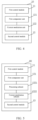
- FIG. 4 is a structural schematic diagram for a control device of a first voltage converter provided in the embodiments of this application.
- the difference between FIG. 4 and FIG. 3 is that the current modulation module 12 of FIG. 4 comprises a first comparator unit 121 and a current modulation unit 122.
- the first comparator unit 121 is used to obtain an output current and the first current threshold and to output a first signal when the absolute value of the output current is greater than the absolute value of the first current threshold.
- the first comparator unit 121 When the first comparator unit 121 outputs a first signal, it means that the output current of a voltage converter is overcurrent.
- a first signal can be a low-level signal when an output current is provided to the non-inverting input terminal of the first comparator unit 121 and the first current threshold is provided to the inverting input terminal of the first comparator unit 121. That is, the first comparator unit 121 outputs a low-level signal when the output current is greater than the first current threshold.
- the first current threshold can be provided by a relevant register, and the user can regulate the first current threshold in the relevant register by software.
- the first current threshold can be set by means of a DA converter that converts digital quantity into analog quantity.
- a first comparator unit comprises a first comparator subsystem (CMPSS).
- CMSS first comparator subsystem
- the following process is required to achieve the overcurrent protection function: multiple current data of circuit to be protected in the preset time period is collected (for characterization of the parameters of actual components in the circuit to be protected) first, then the effective current is screened for multiple current data; and according to the result of screening, the target overcurrent protection value corresponding to the circuit to be protected is determined, which shows that when achieving overcurrent protection through software, the sampling and filtering are required, and the current response time delay is relatively long. Because a short current response time delay is required by the hardware characteristics of a voltage converter switch such as a metal-oxide-semiconductor field-effect transistor (MOSFET), the implementation solutions of pure software are risky.
- MOSFET metal-oxide-semiconductor field-effect transistor
- CMPSS is a component module of digital signal processing (DSP) chip
- DSP digital signal processing
- CMPSS has a high side comparator unit (COMPH), which can compare the positive current with the first current threshold value, and CMPSS further has a low side comparator unit (COMPL), which can compare the negative current with the first current threshold value.
- CMPSS can be used to compare an output current with the first current threshold even though the current flow direction is opposite.
- the first current threshold in a COMPH unit, can be positive, such as 55 amperes (A), and in a COMPL unit, the first current threshold can be negative, such as -55A.
- a positive value of the first current threshold and a negative value of the first current threshold can be obtained through a DA converter.
- the current modulation unit 122 is used to respond to the first signal and reduce the current reference value.
- the current reference value of the current inner loop can be timely regulated through current signal feedback by the first comparator unit 121, without modifying the control parameters of the PI loop, and the overshoot of the PI loop can be avoided to the great extent while ensuring the dynamic response speed of the PI loop.
- FIG. 5 is a structural schematic diagram for a control device of a second voltage converter provided in the embodiments of this application.
- the difference between FIG. 5 and FIG. 4 is that the current modulation unit 122 of FIG. 5 comprises a processing subunit 1221 and a current modulation subunit 1222.
- the processing subunit 1221 is used to determine a current down-regulation value in response to a first signal.
- the current down-regulation value can be a fixed value.
- a current down-regulation value is generated.
- the current modulation subunit 1222 is used to obtain a reduced current reference value after reducing the current down-regulation value from the current reference value.
- the reduced current reference value can be equal to the difference value between the current reference value before the reduction and the current down-regulation value.
- the current modulation subunit 1222 can be concretely implemented as a subtracter. Specifically, a reduced current reference value can be output after the current reference value and a current down-regulation value are inputted to the subtracter.
- FIG. 6 is a structural schematic diagram for a control device of a third voltage converter provided in the embodiments of this application.
- the difference between FIG. 6 and FIG. 3 is that the second control module 13 of FIG. 6 comprises a control unit 131 and a first signal generation unit 132.
- the control unit 131 is used to generate a regulation value of an output current according to the reduced current reference value and an output current.
- control unit 131 can be concretely implemented as a subtracter and a PI controller. Specifically, after the current reference value and an output current are inputted into the PI controller, the difference value between them can be obtained, and then a regulation value of the output current can be obtained through the PI controller.
- the first signal generation unit 132 is used to generate a control signal of a voltage converter according to the regulation value of an output current.
- the first signal generation unit 132 comprises a first enhanced pulse width modulator (ePWM) unit.
- ePWM first enhanced pulse width modulator
- the cycle and the duty ratio of a control signal can be generated by ePWM.
- an ePWM unit and a CMPSS are the component units of the same DSP chip.
- a single DSP chip can be used to control a voltage converter, thus reducing the cost of the hardware circuit.
- the model of the DSP chip can be DSP28337D.
- control unit 131 comprises a difference value determination subunit and a regulation value determination subunit.
- the difference value determination subunit is used to determine the difference value between the reduced current reference value and an output current.
- the difference value determination subunit can be concretely implemented as a subtracter.
- the regulation value determination subunit is used to determine a regulation value according to the difference value.
- the regulation value determination subunit can be concretely implemented as a PI controller.
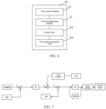
- FIG. 7 is a schematic diagram of an exemplary control logic for a control device of a voltage converter provided in the embodiments of this application.
- a voltage difference value is obtained after the subtraction between an output voltage Vbat of the voltage converter 20 and the given voltage VbatBMS.
- the voltage difference value is subject to PI operation to obtain a current reference value.
- the first CMPSS obtains an output current Iout and outputs a first signal when the absolute value of the output current Iout is greater than the absolute value of the first current threshold.
- the reduced current reference value is obtained. Then the reduced current reference value and an output current Iout are subtracted to obtain the difference value between them. Next, such difference value is subject to PI operation to obtain a regulation value of the output current.
- the PI operation can be implemented by a proportional-integral-resonance (PI-RES) controller.
- the regulation value of an output current is input into the first ePWM unit to obtain a control signal of the voltage converter 20.
- FIG. 8 is a structural schematic diagram for a control device of a fourth voltage converter provided in the embodiments of this application.
- the difference between FIG. 8 and FIG. 3 is that the control device 10 of the voltage converter further in FIG. 8 comprises a third control module 14.
- the third control module 14 is used to control a voltage converter to stop outputting the current when the absolute value of an output current is greater than the absolute value of the second current threshold.
- the absolute value of the second current threshold is greater than the absolute value of the first current threshold.
- the details of the second current threshold can be referred to in the description of the first current threshold, which is not repeated here.
- the second current threshold can be 60A.
- the first and second current thresholds can be set based on actual scenarios and specific requirements, for example, the second current threshold can be set to a preset multiple of the first current threshold, and the preset multiple is greater than 1.
- a severe overshoot may occur when the absolute value of an output current is greater than the absolute value of the second current threshold, for example, the second current threshold can be set according to the maximum allowable current of a voltage converter.
- FIG. 9 is a structural schematic diagram for a control device of a fifth voltage converter provided in the embodiments of this application.
- the difference between FIG. 9 and FIG. 8 is that the third control module 14 of FIG. 9 comprises a second comparator unit 141 and a second signal generation unit 142.
- the second comparator unit 141 is used to obtain an output current and the second current threshold, as well as to output a control instruction when the absolute value of the output current is greater than the absolute value of the second current threshold.
- the control instruction is used to control a voltage converter to stop outputting the current.
- all switching units of the voltage converter 20 can be disconnected to stop outputting the current.
- the second comparator unit 141 comprises a second CMPSS. Please note that the second CMPSS and the first CMPSS can be two different CMPSS.
- the second current threshold in a COMPH unit of the second CMPSS, can be a positive value, such as 60A, and in a COMPL unit of the second CMPSS, the second current threshold can be a negative value, such as -60A.
- the second signal generation unit 142 is further used to generate a control signal for the voltage converter 20 in response to a control instruction.
- the control signal is used to control the converter to stop operating.
- the second signal generation unit 142 comprises an event trip subunit, which modulates a control signal into a low-level signal in response to a control instruction. At this point, a mandatory event is tripped through the event trip subunit and the control signal of the voltage converter 20 are mandatorily modulated into a low-level signal.
- the second signal generation unit comprises a second ePWM unit.
- an event trip subunit can be a trip submodule in the second ePWM unit, and the trip submodule can trip a mandatory event in the second ePWM unit.
- FIG. 10 is a schematic diagram of another exemplary control logic for a control device of a voltage converter provided in the embodiments of this application.
- the second CMPSS may output a control instruction to the second ePWM unit.
- the ePWM unit may trip a mandatory event in response to such control instruction, and the control signal is mandatorily modulated into a low-level signal, controlling the output current Iout to be equal to zero.
- the embodiments of this application further provide a control method for the voltage converter accordingly.
- FIG. 11 is a flow diagram for a control method of a voltage converter provided in the embodiments of this application. As shown in FIG. 11 , the control method for a voltage converter comprises S1110, S1120, and S1130.
- a control method for the voltage converter of the present invention can reduce the current reference value, and the reduced current reference value and an output current can be used to control the output current of the voltage converter.
- the current reference value can be timely reduced when an output current of a voltage converter is overcurrent, so as to achieve a timely regulation of the voltage converter when the output current of the voltage converter is overcurrent.
- S1120 specifically comprises:
- S1130 specifically comprises:
- generating a control signal of a voltage converter according to the regulation value in S1130 specially comprises:
- reducing the current reference value in response to a first signal in S1120 specifically comprises:
- FIG. 12 is a flow schematic diagram for another control method of a voltage converter provided in the embodiments of this application.
- the difference between FIG. 12 and FIG. 11 is that after S1130, the control method of a voltage converter in FIG. 12 further comprises S1140.
- S1140 controlling the voltage converter to stop outputting the current when the absolute value of an output current is greater than the absolute value of the second current threshold.
- the absolute value of the second current threshold is greater than the absolute value of the first current threshold.
- S1140 specifically comprises:
- generating a control signal of the voltage converter in response to the control instruction in S1140 specifically comprises: modulating the control signal into a low-level signal in response to the control instruction.
- control method for the voltage converter according to the embodiments of this application are similar to those of the control device for the voltage converter described above in combination with the examples shown in FIG. 3 through FIG. 10 , and can achieve their corresponding technical effect, which is not repeated here for the sake of simple description.
- FIG. 13 shows a hardware structural schematic diagram for a control device of a voltage converter provided in the embodiments of this application.
- the control device for a voltage converter may comprise a processor 1301 and a memory 1302 that stores computer program instructions.
- the processor 1301 may include a central processing unit (CPU) or an application specific integrated circuit (ASIC), or can be configured into one or more integrated circuit(s) to implement the embodiments of this application.
- CPU central processing unit
- ASIC application specific integrated circuit
- the memory 1302 may comprise a mass memory for data or instructions.
- the memory 1302 may comprise a hard disk drive (HDD), a floppy disk drive, a flash memory, an optical disk, a magneto-optical disk, a magnetic tape, or a universal serial bus (USB) drive or a combination of above two or more thereof.
- the memory 1302 may comprise a removable or non-removable (or fixed) medium, or the memory 1302 is a non-volatile solid-state memory.
- the memory 1302 may be either inside or outside the control device for the voltage converter.
- the memory 1302 may be a read only memory (ROM).
- the ROM may be a mask-programmed ROM, a programmable ROM (PROM), an erasable PROM (EPROM), an electrically erasable PROM (EEPROM), an electrically alterable ROM (EAROM), a flash memory, or a combination of above two or more thereof.
- the memory 1302 may comprise a read-only memory (ROM), a random access memory (RAM), a disk storage medium device, an optical storage medium device, a flash memory device, an electrical, optical, or other physical/tangible memory storage device. Therefore, the memory usually comprises one or more tangible (non-transient) computer readable storage medium(s) (for example, a memory device) coded with software of computer executable instructions, and when such software is executed (for example, by one or more processors), the memory can execute the operation described in the method according to an aspect of this disclosure.
- ROM read-only memory
- RAM random access memory
- the memory usually comprises one or more tangible (non-transient) computer readable storage medium(s) (for example, a memory device) coded with software of computer executable instructions, and when such software is executed (for example, by one or more processors), the memory can execute the operation described in the method according to an aspect of this disclosure.
- the processor 1301 reads and executes the computer program instructions stored in the memory 1302 to achieve the methods in the embodiments shown in FIG. 11 and FIG. 12 and to achieve the corresponding technical effects which can be realized by executing the methods in the embodiments shown in FIG. 11 and FIG. 12 , which is not repeated here for the sake of simple description.
- control device for the voltage converter may further comprise a communication interface 1303 and a bus 1310. As shown in FIG. 13 , the processor 1301, the memory 1302 and the communication interface 1303 are connected and communicate with each other through the bus 1310.
- the communication interface 1303 is used to achieve the communication among modules, devices, units and/or equipment in the embodiments of this application.
- the bus 1310 comprises hardware, software, or both thereof, and couples the components of an online data flow billing device with each other.
- the bus may comprise an accelerated graphics port (AGP) or other graphics buses, an extended industry standard architecture (EISA) bus, a front side bus (FSB), a hyper transport (HT) interconnection, an industry standard architecture (ISA) bus, an InfiniBand interconnect, a low pin count (LPC) bus, a memory bus, a microchannel architecture (MCA) bus, a peripheral component interconnection (PCI) bus, a PCI-Express (PCI-X) bus, a serial advanced technology accessories (SATA) bus, a Video Electronics Standards Association local bus (VLB), other appropriate buses or a combination of above two or more thereof.
- the bus 1310 may comprise one or more buses. Although specific buses are described and shown in the embodiments of this application, any suitable bus or interconnection is considered in this application.
- the control device for such voltage converter can execute the control method for the voltage converter in the embodiments of this application, so as to achieve the control method and the device for the voltage converter described in combination with FIG. 3 through FIG. 12 .
- the embodiments of this application can provide a computer storage medium to achieve the control method for the voltage converter in combination with the above embodiments.
- the computer storage medium is stored with computer program instructions; when the computer program instructions are executed by the processor, any control method for the voltage converter in the above embodiments can be achieved.
- the functional blocks shown in the structural block diagram above can be implemented in hardware, software, firmware or a combination thereof. When implemented in hardware, this can be, for example, an electronic circuit, an application specific integrated circuit (ASIC), an appropriate firmware, a plug-in, or a functional card.
- ASIC application specific integrated circuit
- the elements of this application are the program or code segment that is used to execute the required task.
- a program or a code segment can be stored in a machine-readable medium or transmitted over a transmission medium or communication link by a data signal carried on a carrier.
- the "machine-readable medium” may comprise any medium capable of storing or transmitting the information.
- machine-readable medium comprise an electronic circuit, a semiconductor memory device, a ROM, a flash memory, an erasable ROM (EROM), a floppy disk, a CD-ROM, an optical disk, a hard disk, an optical fiber medium, a radio frequency (RF) link and so on.
- the code segment can be downloaded over computer networks such as the Internet and intranets.
- each box in the flow chart and/or block diagram and the combination of the boxes in the flow chart and/or block diagram can be implemented by computer program instructions.
- These computer program instructions can be provided to a general-purpose computer, a special-purpose computer or a processor for other programmable data processing devices to produce a machine, so that these instructions executed by the computer or the processor for other programmable data processing devices can trigger the implementation of designated functions/actions in the one or more boxes of the flow chart and/or block diagram.
- Such a processor may be but is not limited to a general-purpose processor, a special-purpose processor, a special-application processor, or a field programmable logic circuit.
- each box in the block diagram and/or flow chart and the combination of boxes in the block diagram and/or flow chart may further either be implemented by dedicated hardware executing a designated function or action, or by a combination of dedicated hardware and computer instructions.
Landscapes
- Engineering & Computer Science (AREA)
- Power Engineering (AREA)
- Dc-Dc Converters (AREA)
- Rectifiers (AREA)
- Inverter Devices (AREA)
Claims (13)
- Steuereinrichtung (10) für Überstromschutz für einen Spannungswandler (20), umfassend:ein erstes Steuermodul (11), das konfiguriert ist, um einen Stromreferenzwert in Abhängigkeit von einer Ausgangsspannung des Spannungswandlers (20) und einem vorgegebenen Spannungswert zu erhalten;ein Strommodulationsmodul (12), das konfiguriert ist, um den Stromreferenzwert zu verringern, wenn ein Absolutwert eines Ausgangsstroms des Spannungswandlers (20) größer als ein Absolutwert eines ersten Stromschwellenwerts ist, wobei das Strommodulationsmodul (12) Folgendes umfasst:eine erste Komparatoreinheit (121), die ein erstes Komparatoruntersystem, CMPSS, umfasst, das konfiguriert ist, um den Ausgangsstrom und den ersten Stromschwellenwert zu erhalten und ein erstes Signal auszugeben, wenn der Absolutwert des Ausgangsstroms größer als der Absolutwert des ersten Stromschwellenwerts ist, wobei das CMPSS eine Komponente eines Digitalsignalverarbeitungschips, DSP-Chips, ist, undeine Strommodulationseinheit (122), die konfiguriert ist, um den Stromreferenzwert als Reaktion auf das erste Signal zu verringern, dadurch gekennzeichnet, dassdie Strommodulationseinheit (122) Folgendes umfasst:eine Verarbeitungsuntereinheit (1221), die konfiguriert ist, um einen Stromabwärtsregelungswert als Reaktion auf das erste Signal zu bestimmen, wobei der Stromabwärtsregelungswert ein Festwert ist, undeine Strommodulationsuntereinheit (1222), die konfiguriert ist, um den Stromreferenzwert um den Stromabwärtsregelungswert zu verringern, um den verringerten Stromreferenzwert zu erhalten; und die Steuereinrichtung (10) Folgendes umfasst:ein zweites Steuermodul (13), das konfiguriert ist, um den Ausgangsstrom des Spannungswandlers (20) in Abhängigkeit von dem verringerten Stromreferenzwert und dem Ausgangsstrom zu steuern.
- Steuereinrichtung (10) nach Anspruch 1, wobei das zweite Steuermodul (13) Folgendes umfasst:eine Steuereinheit (131), die konfiguriert ist, um einen Regelungswert des Ausgangsstroms in Abhängigkeit von dem verringerten Stromreferenzwert und dem Ausgangsstrom zu erzeugen;eine erste Signalerzeugungseinheit (132), die konfiguriert ist, um ein Steuersignal des Spannungswandlers (20) in Abhängigkeit von dem Regelungswert zu erzeugen, um den Ausgangsstrom des Spannungswandlers (20) durch das Steuersignal zu steuern, wobei vorzugsweise die erste Signalerzeugungseinheit (132) eine erste enhanced-Pulse-Width-Modulation-Einheit, ePWM-Einheit, umfasst.
- Steuereinrichtung (10) nach Anspruch 2, wobei die Steuereinheit (131) Folgendes umfasst:eine Differenzwertbestimmungsuntereinheit, die konfiguriert ist, um einen Differenzwert zwischen dem verringerten Stromreferenzwert und dem Ausgangsstrom zu bestimmen; undeine Regelungswertbestimmungsuntereinheit, die konfiguriert ist, um den Regelungswert in Abhängigkeit von dem Differenzwert zu bestimmen.
- Steuereinrichtung (10) nach einem der Ansprüche 1 bis 3, wobei die Steuereinrichtung (10) ferner Folgendes umfasst:ein drittes Steuermodul (14), das konfiguriert ist, um den Spannungswandler (20) zum Unterbrechen des Ausgebens von Strom, wenn der Absolutwert des Ausgangsstroms größer als ein Absolutwert eines zweiten Stromschwellenwerts ist, zu steuern,wobei der Absolutwert des zweiten Stromschwellenwerts größer als der Absolutwert des ersten Stromschwellenwerts ist.
- Steuereinrichtung (10) nach Anspruch 4, wobei das dritte Steuermodul (14) Folgendes umfasst:eine zweite Komparatoreinheit (141), die konfiguriert ist, um den Ausgangsstrom und den zweiten Stromschwellenwert zu erhalten und einen Steuerbefehl auszugeben, wenn der Absolutwert des Ausgangsstroms größer als der Absolutwert des zweiten Stromschwellenwerts ist, wobei der Steuerbefehl konfiguriert ist, um den Spannungswandler (20) zum Unterbrechen des Ausgebens von Strom zu steuern; undeine zweite Signalerzeugungseinheit (142), die konfiguriert ist, um das Steuersignal des Spannungswandlers (20) als Reaktion auf den Steuerbefehl zu erzeugen.
- Steuereinrichtung (10) nach Anspruch 5, wobei die zweite Komparatoreinheit (141) ein zweites CMPSS umfasst.
- Steuereinrichtung (10) nach Anspruch 5 oder 6, wobei die zweite Signalerzeugungseinheit (142) eine Ereignisauslösungsuntereinheit umfasst, die konfiguriert ist, um das Steuersignal als Reaktion auf den Steuerbefehl in ein Low-Signal zu modulieren.
- Steuereinrichtung (10) nach einem der Ansprüche 5 bis 7, wobei die zweite Signalerzeugungseinheit eine zweite ePWM-Einheit umfasst.
- Steuereinrichtung (10) nach einem der Ansprüche 1 bis 8, wobei ein Ende des Spannungswandlers (20) mit einer Batterie (30) verbunden ist und das andere Ende des Spannungswandlers (20) mit einem Stromnetz oder einem Wechselstromverbraucher verbunden ist.
- Verfahren zum Überstromschutz für einen Spannungswandler (20) unter Nutzung einer Steuereinrichtung nach einem der vorhergehenden Ansprüche, umfassend:Erhalten eines Stromreferenzwerts in Abhängigkeit von einer Ausgangsspannung des Spannungswandlers (20) und einem vorgegebenen Spannungswert;Verringern des Stromreferenzwerts, wenn ein Absolutwert eines Ausgangsstroms des Spannungswandlers (20) größer als ein Absolutwert eines ersten Stromschwellenwerts ist, wobei der erste Stromschwellenwert einen Schwellenwert zwischen Überstrom und Nicht-Überstrom des Spannungswandlers (20) darstellt; durch Folgendes:Erhalten des Ausgangsstroms und des ersten Stromschwellenwerts und Ausgeben eines ersten Signals, wenn der Absolutwert des Ausgangsstroms größer als der Absolutwert des ersten Stromschwellenwerts ist, undVerringern des Stromreferenzwerts als Reaktion auf das erste Signal durch Folgendes:Bestimmen eines Stromabwärtsregelungswerts als Reaktion auf das erste Signal, wobei der Stromabwärtsregelungswert ein Festwert ist, undVerringern des Stromreferenzwerts um denStromabwärtsregelungswert, um den verringerten Stromreferenzwert zu erhalten; undSteuern des Ausgangsstroms des Spannungswandlers (20) in Abhängigkeit von dem verringerten Stromreferenzwert und dem Ausgangsstrom.
- Verfahren nach Anspruch 10, wobei das Steuern des Ausgangsstroms des Spannungswandlers (20) in Abhängigkeit von dem verringerten Stromreferenzwert und dem Ausgangsstrom ferner Folgendes umfasst:Erzeugen eines Abwärtsregelungswerts des Ausgangsstroms in Abhängigkeit von dem verringerten Stromreferenzwert und dem Ausgangsstrom; undErzeugen eines Steuersignals des Spannungswandlers (20) in Abhängigkeit von dem Regelungswert, um den Ausgangsstrom des Spannungswandlers (20) durch das Steuersignal zu steuern; und/oderdas Verfahren nach dem Erhalten eines Stromreferenzwerts in Abhängigkeit von einer Ausgangsspannung des Spannungswandlers (20) und einem vorgegebenen Spannungswert ferner das Steuern des Spannungswandlers (20) zum Unterbrechen des Ausgebens von Strom, wenn der Absolutwert des Ausgangsstroms größer als der Absolutwert des zweiten Stromschwellenwerts ist, umfasst, wobei ein Absolutwert des zweiten Stromschwellenwerts größer als der Absolutwert des ersten Stromschwellenwerts ist.
- Spannungssteuerungssystem, umfassend:die Steuereinrichtung (10) für einen Spannungswandler (20) nach einem der Ansprüche 1 bis 9; undden Spannungswandler (20).
- Computerspeichermedium, in dem Computerprogrammbefehle gespeichert sind, wobei die Computerprogrammbefehle, wenn sie von einem Prozessor (1301) ausgeführt werden, das Verfahren zum Überstromschutz nach Anspruch 10 oder 11 zum Schützen des Systems nach Anspruch 12 implementieren.
Applications Claiming Priority (2)
| Application Number | Priority Date | Filing Date | Title |
|---|---|---|---|
| CN202011620158.0A CN112290776B (zh) | 2020-12-31 | 2020-12-31 | 电压变换器的控制方法、装置以及电压控制系统 |
| PCT/CN2021/129511 WO2022142745A1 (zh) | 2020-12-31 | 2021-11-09 | 电压变换器的控制方法、装置以及电压控制系统 |
Publications (3)
| Publication Number | Publication Date |
|---|---|
| EP4075650A1 EP4075650A1 (de) | 2022-10-19 |
| EP4075650A4 EP4075650A4 (de) | 2023-08-02 |
| EP4075650B1 true EP4075650B1 (de) | 2025-05-14 |
Family
ID=74425354
Family Applications (1)
| Application Number | Title | Priority Date | Filing Date |
|---|---|---|---|
| EP21913488.9A Active EP4075650B1 (de) | 2020-12-31 | 2021-11-09 | Verfahren und vorrichtung zur steuerung eines spannungswandlers und spannungssteuerungssystem |
Country Status (6)
| Country | Link |
|---|---|
| US (1) | US11962231B2 (de) |
| EP (1) | EP4075650B1 (de) |
| JP (1) | JP7316458B2 (de) |
| KR (1) | KR102720946B1 (de) |
| CN (1) | CN112290776B (de) |
| WO (1) | WO2022142745A1 (de) |
Families Citing this family (3)
| Publication number | Priority date | Publication date | Assignee | Title |
|---|---|---|---|---|
| CN112290776B (zh) * | 2020-12-31 | 2021-06-08 | 江苏时代新能源科技有限公司 | 电压变换器的控制方法、装置以及电压控制系统 |
| CN114785119B (zh) * | 2022-03-26 | 2026-05-08 | 深圳欣锐科技股份有限公司 | Dcdc变换器的输出电压调节方法及相关装置 |
| FR3154358A1 (fr) * | 2023-10-20 | 2025-04-25 | Vitesco Technologies | Dispositif de commande de convertisseur, véhicule et procédé de commande associés |
Citations (2)
| Publication number | Priority date | Publication date | Assignee | Title |
|---|---|---|---|---|
| US5838524A (en) * | 1997-03-21 | 1998-11-17 | Cherry Semiconductor Corporation | Current limit circuit for inhibiting voltage overshoot |
| EP1199791A2 (de) * | 2000-10-12 | 2002-04-24 | GSPK Electronics Limited | Schaltung eines Leistungsumwandlers |
Family Cites Families (17)
| Publication number | Priority date | Publication date | Assignee | Title |
|---|---|---|---|---|
| US6700360B2 (en) * | 2002-03-25 | 2004-03-02 | Texas Instruments Incorporated | Output stage compensation circuit |
| CN100442620C (zh) * | 2005-02-03 | 2008-12-10 | 昂宝电子(上海)有限公司 | 用于开关电源变换器的多阈值过流保护的系统和方法 |
| JP4691404B2 (ja) * | 2005-06-24 | 2011-06-01 | 三洋電機株式会社 | スイッチング制御回路、自励型dc−dcコンバータ |
| TWI357204B (en) * | 2008-09-25 | 2012-01-21 | Advanced Analog Technology Inc | A low drop out regulator with over-current protect |
| CN103078298B (zh) | 2013-01-12 | 2015-09-02 | 华南理工大学 | 一种igbt的过流分级保护电路及控制方法 |
| CN103078485B (zh) * | 2013-01-28 | 2015-08-19 | 华为技术有限公司 | 一种逆变器输出限流保护方法及装置 |
| CN103280960B (zh) * | 2013-05-31 | 2015-04-15 | 华为技术有限公司 | 限流装置及限流方法 |
| CN104423407B (zh) * | 2013-08-28 | 2016-05-25 | 联发科技(新加坡)私人有限公司 | 低压差线性稳压器及其启动方法、电子装置和芯片 |
| US9379625B2 (en) * | 2013-12-26 | 2016-06-28 | Dialog Semiconductor Inc. | Current meter for load modulation communication receiver architecture |
| CN106385101B (zh) * | 2016-09-22 | 2020-03-20 | 广东寰宇电子科技股份有限公司 | 一种大功率型电梯自动救援装置实现供电的方法及装置 |
| JP6747964B2 (ja) | 2016-12-22 | 2020-08-26 | 東芝テック株式会社 | 非接触給電装置及びプログラム |
| CN108011506A (zh) * | 2017-11-23 | 2018-05-08 | 郑州云海信息技术有限公司 | 一种逆变器的限流控制方法及系统 |
| US11271483B2 (en) * | 2018-10-17 | 2022-03-08 | Texas Instruments Incorporated | Bias power regulator circuit for isolated converters with a wide output voltage range |
| US10951036B2 (en) * | 2019-07-03 | 2021-03-16 | Neworld.Energy Llc | Grid-tied variable frequency facility |
| CN110707657B (zh) | 2019-10-28 | 2022-01-28 | 深圳市施罗德工业集团有限公司 | 一种过流保护设定方法、过流保护方法及装置 |
| JP6824362B1 (ja) | 2019-10-28 | 2021-02-03 | 三菱電機株式会社 | 電力変換装置 |
| CN112290776B (zh) * | 2020-12-31 | 2021-06-08 | 江苏时代新能源科技有限公司 | 电压变换器的控制方法、装置以及电压控制系统 |
-
2020
- 2020-12-31 CN CN202011620158.0A patent/CN112290776B/zh active Active
-
2021
- 2021-11-09 EP EP21913488.9A patent/EP4075650B1/de active Active
- 2021-11-09 WO PCT/CN2021/129511 patent/WO2022142745A1/zh not_active Ceased
- 2021-11-09 KR KR1020227019648A patent/KR102720946B1/ko active Active
- 2021-11-09 JP JP2022534389A patent/JP7316458B2/ja active Active
-
2022
- 2022-08-24 US US17/821,811 patent/US11962231B2/en active Active
Patent Citations (2)
| Publication number | Priority date | Publication date | Assignee | Title |
|---|---|---|---|---|
| US5838524A (en) * | 1997-03-21 | 1998-11-17 | Cherry Semiconductor Corporation | Current limit circuit for inhibiting voltage overshoot |
| EP1199791A2 (de) * | 2000-10-12 | 2002-04-24 | GSPK Electronics Limited | Schaltung eines Leistungsumwandlers |
Non-Patent Citations (2)
| Title |
|---|
| "Pulse-Width Modulated DC-DC Power Converters", 16 September 2008, JOHN WILEY & SONS, LTD., U.K., ISBN: 978-0-47-069464-0, article MARIAN K. KAZIMIERCZUK: "Chapter 13: Current-mode Control", pages: 511 - 570, XP055174330, DOI: 10.1002/9780470694640.ch13 * |
| ZHONG WU ET AL: "Cascade PID Control of Buck-Boost-Type DC/DC Power Converters", INTELLIGENT CONTROL AND AUTOMATION, 2006. WCICA 2006. THE SIXTH WORLD CONGRESS ON DALIAN, CHINA 21-23 JUNE 2006, PISCATAWAY, NJ, USA,IEEE, vol. 2, 21 June 2006 (2006-06-21), pages 8467 - 8471, XP010946730, ISBN: 978-1-4244-0332-5, DOI: 10.1109/WCICA.2006.1713630 * |
Also Published As
| Publication number | Publication date |
|---|---|
| JP2023511819A (ja) | 2023-03-23 |
| KR20220100633A (ko) | 2022-07-15 |
| US11962231B2 (en) | 2024-04-16 |
| CN112290776A (zh) | 2021-01-29 |
| EP4075650A4 (de) | 2023-08-02 |
| KR102720946B1 (ko) | 2024-10-22 |
| CN112290776B (zh) | 2021-06-08 |
| US20230044189A1 (en) | 2023-02-09 |
| WO2022142745A1 (zh) | 2022-07-07 |
| EP4075650A1 (de) | 2022-10-19 |
| JP7316458B2 (ja) | 2023-07-27 |
Similar Documents
| Publication | Publication Date | Title |
|---|---|---|
| US11962231B2 (en) | Control method and device of voltage converter and voltage control system | |
| US11290801B2 (en) | Headset charging system and headset charging method | |
| CN112736311B (zh) | 蓄电池的充电方法、装置和电子设备 | |
| CN108292889B (zh) | 电源装置、电源装置的控制方法以及记录介质 | |
| US20220271684A1 (en) | Power converter | |
| CN110601283A (zh) | 一种充电方法与系统 | |
| US20250058668A1 (en) | Charging control method, control device, charging pile, and charging system | |
| AU2019291494B2 (en) | Quick charging method for battery, charging apparatus, device to be charged, and charging system | |
| EP3323666A1 (de) | Elektrofahrzeugversorgungsausrüstung mit mehrere leistungsmodule und ladeverfahren | |
| US9634500B2 (en) | Storage battery system | |
| CN115946544A (zh) | 新能源汽车功率控制方法、装置、设备及可读存储介质 | |
| US20160082851A1 (en) | Charging system and charging method | |
| US12580393B2 (en) | Control method of battery apparatus and battery apparatus, system, and medium | |
| EP4131572A1 (de) | Batteriepack und steuerungsverfahren für batteriepack | |
| CN210517805U (zh) | 一种开关频率可自动调节的储能变流器 | |
| CN120039138A (zh) | 充电控制方法、装置、bms、存储介质及计算机程序产品 | |
| EP4080716B1 (de) | Schutzschaltung, hochspannungsschleife, elektrisches gerät, steuerverfahren, vorrichtung und medium | |
| CN111551859B (zh) | 电池可用电量计量方法、计算机装置以及计算机可读存储介质 | |
| EP4645663A1 (de) | Parallelstromversorgungsvorrichtung und programm | |
| CN114709832B (zh) | 牵引供电系统和飞轮储能装置联用的控制方法及装置 | |
| EP3982139A1 (de) | Schaltungsdiagnosevorrichtung und batteriesatz damit | |
| CN114162109A (zh) | 增程器功率控制方法、装置、用电装置、电子设备及车辆 | |
| EP4362255A1 (de) | Forsmark-effekt-überwachungsverfahren für nukleare elektrische ausrüstung | |
| CN121043641A (zh) | 太阳能充电系统 | |
| CN119459454A (zh) | 充放电控制方法、装置、设备、存储介质及系统 |
Legal Events
| Date | Code | Title | Description |
|---|---|---|---|
| STAA | Information on the status of an ep patent application or granted ep patent |
Free format text: STATUS: THE INTERNATIONAL PUBLICATION HAS BEEN MADE |
|
| PUAI | Public reference made under article 153(3) epc to a published international application that has entered the european phase |
Free format text: ORIGINAL CODE: 0009012 |
|
| STAA | Information on the status of an ep patent application or granted ep patent |
Free format text: STATUS: REQUEST FOR EXAMINATION WAS MADE |
|
| 17P | Request for examination filed |
Effective date: 20220715 |
|
| AK | Designated contracting states |
Kind code of ref document: A1 Designated state(s): AL AT BE BG CH CY CZ DE DK EE ES FI FR GB GR HR HU IE IS IT LI LT LU LV MC MK MT NL NO PL PT RO RS SE SI SK SM TR |
|
| A4 | Supplementary search report drawn up and despatched |
Effective date: 20230703 |
|
| RIC1 | Information provided on ipc code assigned before grant |
Ipc: H02M 7/5387 20070101ALN20230627BHEP Ipc: H02M 7/48 20070101ALN20230627BHEP Ipc: H02M 1/32 20070101ALI20230627BHEP Ipc: H02M 1/00 20060101AFI20230627BHEP |
|
| STAA | Information on the status of an ep patent application or granted ep patent |
Free format text: STATUS: EXAMINATION IS IN PROGRESS |
|
| 17Q | First examination report despatched |
Effective date: 20240105 |
|
| DAV | Request for validation of the european patent (deleted) | ||
| DAX | Request for extension of the european patent (deleted) | ||
| GRAP | Despatch of communication of intention to grant a patent |
Free format text: ORIGINAL CODE: EPIDOSNIGR1 |
|
| STAA | Information on the status of an ep patent application or granted ep patent |
Free format text: STATUS: GRANT OF PATENT IS INTENDED |
|
| RIC1 | Information provided on ipc code assigned before grant |
Ipc: H02M 7/5387 20070101ALN20250116BHEP Ipc: H02M 7/48 20070101ALN20250116BHEP Ipc: H02M 1/32 20070101ALI20250116BHEP Ipc: H02M 1/00 20060101AFI20250116BHEP |
|
| RIC1 | Information provided on ipc code assigned before grant |
Ipc: H02M 7/5387 20070101ALN20250121BHEP Ipc: H02M 7/48 20070101ALN20250121BHEP Ipc: H02M 1/32 20070101ALI20250121BHEP Ipc: H02M 1/00 20060101AFI20250121BHEP |
|
| INTG | Intention to grant announced |
Effective date: 20250203 |
|
| RIC1 | Information provided on ipc code assigned before grant |
Ipc: H02M 7/5387 20070101ALN20250127BHEP Ipc: H02M 7/48 20070101ALN20250127BHEP Ipc: H02M 1/32 20070101ALI20250127BHEP Ipc: H02M 1/00 20060101AFI20250127BHEP |
|
| GRAS | Grant fee paid |
Free format text: ORIGINAL CODE: EPIDOSNIGR3 |
|
| GRAA | (expected) grant |
Free format text: ORIGINAL CODE: 0009210 |
|
| STAA | Information on the status of an ep patent application or granted ep patent |
Free format text: STATUS: THE PATENT HAS BEEN GRANTED |
|
| AK | Designated contracting states |
Kind code of ref document: B1 Designated state(s): AL AT BE BG CH CY CZ DE DK EE ES FI FR GB GR HR HU IE IS IT LI LT LU LV MC MK MT NL NO PL PT RO RS SE SI SK SM TR |
|
| REG | Reference to a national code |
Ref country code: GB Ref legal event code: FG4D |
|
| REG | Reference to a national code |
Ref country code: CH Ref legal event code: EP |
|
| P01 | Opt-out of the competence of the unified patent court (upc) registered |
Free format text: CASE NUMBER: APP_19284/2025 Effective date: 20250422 |
|
| REG | Reference to a national code |
Ref country code: DE Ref legal event code: R096 Ref document number: 602021030953 Country of ref document: DE |
|
| REG | Reference to a national code |
Ref country code: IE Ref legal event code: FG4D |
|
| REG | Reference to a national code |
Ref country code: NL Ref legal event code: FP |
|
| PG25 | Lapsed in a contracting state [announced via postgrant information from national office to epo] |
Ref country code: PT Free format text: LAPSE BECAUSE OF FAILURE TO SUBMIT A TRANSLATION OF THE DESCRIPTION OR TO PAY THE FEE WITHIN THE PRESCRIBED TIME-LIMIT Effective date: 20250915 Ref country code: FI Free format text: LAPSE BECAUSE OF FAILURE TO SUBMIT A TRANSLATION OF THE DESCRIPTION OR TO PAY THE FEE WITHIN THE PRESCRIBED TIME-LIMIT Effective date: 20250514 Ref country code: ES Free format text: LAPSE BECAUSE OF FAILURE TO SUBMIT A TRANSLATION OF THE DESCRIPTION OR TO PAY THE FEE WITHIN THE PRESCRIBED TIME-LIMIT Effective date: 20250514 |
|
| REG | Reference to a national code |
Ref country code: LT Ref legal event code: MG9D |
|
| PG25 | Lapsed in a contracting state [announced via postgrant information from national office to epo] |
Ref country code: GR Free format text: LAPSE BECAUSE OF FAILURE TO SUBMIT A TRANSLATION OF THE DESCRIPTION OR TO PAY THE FEE WITHIN THE PRESCRIBED TIME-LIMIT Effective date: 20250815 |
|
| PG25 | Lapsed in a contracting state [announced via postgrant information from national office to epo] |
Ref country code: PL Free format text: LAPSE BECAUSE OF FAILURE TO SUBMIT A TRANSLATION OF THE DESCRIPTION OR TO PAY THE FEE WITHIN THE PRESCRIBED TIME-LIMIT Effective date: 20250514 |
|
| REG | Reference to a national code |
Ref country code: AT Ref legal event code: MK05 Ref document number: 1795672 Country of ref document: AT Kind code of ref document: T Effective date: 20250514 |
|
| PG25 | Lapsed in a contracting state [announced via postgrant information from national office to epo] |
Ref country code: BG Free format text: LAPSE BECAUSE OF FAILURE TO SUBMIT A TRANSLATION OF THE DESCRIPTION OR TO PAY THE FEE WITHIN THE PRESCRIBED TIME-LIMIT Effective date: 20250514 |
|
| PG25 | Lapsed in a contracting state [announced via postgrant information from national office to epo] |
Ref country code: HR Free format text: LAPSE BECAUSE OF FAILURE TO SUBMIT A TRANSLATION OF THE DESCRIPTION OR TO PAY THE FEE WITHIN THE PRESCRIBED TIME-LIMIT Effective date: 20250514 |
|
| PG25 | Lapsed in a contracting state [announced via postgrant information from national office to epo] |
Ref country code: AT Free format text: LAPSE BECAUSE OF FAILURE TO SUBMIT A TRANSLATION OF THE DESCRIPTION OR TO PAY THE FEE WITHIN THE PRESCRIBED TIME-LIMIT Effective date: 20250514 |
|
| PG25 | Lapsed in a contracting state [announced via postgrant information from national office to epo] |
Ref country code: RS Free format text: LAPSE BECAUSE OF FAILURE TO SUBMIT A TRANSLATION OF THE DESCRIPTION OR TO PAY THE FEE WITHIN THE PRESCRIBED TIME-LIMIT Effective date: 20250814 |
|
| PG25 | Lapsed in a contracting state [announced via postgrant information from national office to epo] |
Ref country code: IS Free format text: LAPSE BECAUSE OF FAILURE TO SUBMIT A TRANSLATION OF THE DESCRIPTION OR TO PAY THE FEE WITHIN THE PRESCRIBED TIME-LIMIT Effective date: 20250914 |
|
| PG25 | Lapsed in a contracting state [announced via postgrant information from national office to epo] |
Ref country code: LV Free format text: LAPSE BECAUSE OF FAILURE TO SUBMIT A TRANSLATION OF THE DESCRIPTION OR TO PAY THE FEE WITHIN THE PRESCRIBED TIME-LIMIT Effective date: 20250514 |
|
| PGFP | Annual fee paid to national office [announced via postgrant information from national office to epo] |
Ref country code: NL Payment date: 20251127 Year of fee payment: 5 |
|
| PGFP | Annual fee paid to national office [announced via postgrant information from national office to epo] |
Ref country code: DE Payment date: 20251124 Year of fee payment: 5 |
|
| PGFP | Annual fee paid to national office [announced via postgrant information from national office to epo] |
Ref country code: GB Payment date: 20251126 Year of fee payment: 5 |
|
| PGFP | Annual fee paid to national office [announced via postgrant information from national office to epo] |
Ref country code: NO Payment date: 20251125 Year of fee payment: 5 |
|
| PG25 | Lapsed in a contracting state [announced via postgrant information from national office to epo] |
Ref country code: DK Free format text: LAPSE BECAUSE OF FAILURE TO SUBMIT A TRANSLATION OF THE DESCRIPTION OR TO PAY THE FEE WITHIN THE PRESCRIBED TIME-LIMIT Effective date: 20250514 Ref country code: SM Free format text: LAPSE BECAUSE OF FAILURE TO SUBMIT A TRANSLATION OF THE DESCRIPTION OR TO PAY THE FEE WITHIN THE PRESCRIBED TIME-LIMIT Effective date: 20250514 |
|
| PG25 | Lapsed in a contracting state [announced via postgrant information from national office to epo] |
Ref country code: CZ Free format text: LAPSE BECAUSE OF FAILURE TO SUBMIT A TRANSLATION OF THE DESCRIPTION OR TO PAY THE FEE WITHIN THE PRESCRIBED TIME-LIMIT Effective date: 20250514 |
|
| PG25 | Lapsed in a contracting state [announced via postgrant information from national office to epo] |
Ref country code: EE Free format text: LAPSE BECAUSE OF FAILURE TO SUBMIT A TRANSLATION OF THE DESCRIPTION OR TO PAY THE FEE WITHIN THE PRESCRIBED TIME-LIMIT Effective date: 20250514 |
|
| PG25 | Lapsed in a contracting state [announced via postgrant information from national office to epo] |
Ref country code: SK Free format text: LAPSE BECAUSE OF FAILURE TO SUBMIT A TRANSLATION OF THE DESCRIPTION OR TO PAY THE FEE WITHIN THE PRESCRIBED TIME-LIMIT Effective date: 20250514 |
|
| PG25 | Lapsed in a contracting state [announced via postgrant information from national office to epo] |
Ref country code: IT Free format text: LAPSE BECAUSE OF FAILURE TO SUBMIT A TRANSLATION OF THE DESCRIPTION OR TO PAY THE FEE WITHIN THE PRESCRIBED TIME-LIMIT Effective date: 20250514 |
|
| PG25 | Lapsed in a contracting state [announced via postgrant information from national office to epo] |
Ref country code: RO Free format text: LAPSE BECAUSE OF FAILURE TO SUBMIT A TRANSLATION OF THE DESCRIPTION OR TO PAY THE FEE WITHIN THE PRESCRIBED TIME-LIMIT Effective date: 20250514 |
|
| REG | Reference to a national code |
Ref country code: DE Ref legal event code: R097 Ref document number: 602021030953 Country of ref document: DE |
|
| PLBE | No opposition filed within time limit |
Free format text: ORIGINAL CODE: 0009261 |
|
| STAA | Information on the status of an ep patent application or granted ep patent |
Free format text: STATUS: NO OPPOSITION FILED WITHIN TIME LIMIT |
|
| REG | Reference to a national code |
Ref country code: CH Ref legal event code: L10 Free format text: ST27 STATUS EVENT CODE: U-0-0-L10-L00 (AS PROVIDED BY THE NATIONAL OFFICE) Effective date: 20260325 |
|
| 26N | No opposition filed |
Effective date: 20260217 |