EP4075169A1 - Radiation detector module, radiation detector, and x-ray ct apparatus - Google Patents
Radiation detector module, radiation detector, and x-ray ct apparatus Download PDFInfo
- Publication number
- EP4075169A1 EP4075169A1 EP22167931.9A EP22167931A EP4075169A1 EP 4075169 A1 EP4075169 A1 EP 4075169A1 EP 22167931 A EP22167931 A EP 22167931A EP 4075169 A1 EP4075169 A1 EP 4075169A1
- Authority
- EP
- European Patent Office
- Prior art keywords
- electrode
- mark
- radiation detector
- radiation
- ray
- Prior art date
- Legal status (The legal status is an assumption and is not a legal conclusion. Google has not performed a legal analysis and makes no representation as to the accuracy of the status listed.)
- Granted
Links
Images






Classifications
-
- G—PHYSICS
- G01—MEASURING; TESTING
- G01T—MEASUREMENT OF NUCLEAR OR X-RADIATION
- G01T1/00—Measuring X-radiation, gamma radiation, corpuscular radiation, or cosmic radiation
- G01T1/16—Measuring radiation intensity
- G01T1/24—Measuring radiation intensity with semiconductor detectors
- G01T1/243—Modular detectors, e.g. arrays formed from self contained units
-
- G—PHYSICS
- G01—MEASURING; TESTING
- G01T—MEASUREMENT OF NUCLEAR OR X-RADIATION
- G01T1/00—Measuring X-radiation, gamma radiation, corpuscular radiation, or cosmic radiation
- G01T1/16—Measuring radiation intensity
-
- G—PHYSICS
- G01—MEASURING; TESTING
- G01N—INVESTIGATING OR ANALYSING MATERIALS BY DETERMINING THEIR CHEMICAL OR PHYSICAL PROPERTIES
- G01N23/00—Investigating or analysing materials by the use of wave or particle radiation, e.g. X-rays or neutrons, not covered by groups G01N3/00 – G01N17/00, G01N21/00 or G01N22/00
- G01N23/02—Investigating or analysing materials by the use of wave or particle radiation, e.g. X-rays or neutrons, not covered by groups G01N3/00 – G01N17/00, G01N21/00 or G01N22/00 by transmitting the radiation through the material
- G01N23/04—Investigating or analysing materials by the use of wave or particle radiation, e.g. X-rays or neutrons, not covered by groups G01N3/00 – G01N17/00, G01N21/00 or G01N22/00 by transmitting the radiation through the material and forming images of the material
- G01N23/046—Investigating or analysing materials by the use of wave or particle radiation, e.g. X-rays or neutrons, not covered by groups G01N3/00 – G01N17/00, G01N21/00 or G01N22/00 by transmitting the radiation through the material and forming images of the material using tomography, e.g. computed tomography [CT]
-
- A—HUMAN NECESSITIES
- A61—MEDICAL OR VETERINARY SCIENCE; HYGIENE
- A61B—DIAGNOSIS; SURGERY; IDENTIFICATION
- A61B6/00—Apparatus or devices for radiation diagnosis; Apparatus or devices for radiation diagnosis combined with radiation therapy equipment
- A61B6/02—Arrangements for diagnosis sequentially in different planes; Stereoscopic radiation diagnosis
- A61B6/03—Computed tomography [CT]
- A61B6/032—Transmission computed tomography [CT]
-
- A—HUMAN NECESSITIES
- A61—MEDICAL OR VETERINARY SCIENCE; HYGIENE
- A61B—DIAGNOSIS; SURGERY; IDENTIFICATION
- A61B6/00—Apparatus or devices for radiation diagnosis; Apparatus or devices for radiation diagnosis combined with radiation therapy equipment
- A61B6/42—Arrangements for detecting radiation specially adapted for radiation diagnosis
- A61B6/4208—Arrangements for detecting radiation specially adapted for radiation diagnosis characterised by using a particular type of detector
- A61B6/4233—Arrangements for detecting radiation specially adapted for radiation diagnosis characterised by using a particular type of detector using matrix detectors
Definitions
- Embodiments disclosed in the present description and drawings relate to a radiation detector module, a radiation detector, and an X-ray CT apparatus.
- a plurality of radiation detector modules are arranged side by side in a radiation detector.
- the accuracy of positioning of the radiation detector modules has a great influence on the detection accuracy of the radiation detector.
- Positioning of radiation detector modules has been performed, for example, on the basis of pins provided on a mounting part of the radiation detector modules.
- a problem to be solved by the embodiments disclosed in the present description and the drawings is to improve the positioning accuracy of radiation detector modules.
- the problems to be solved by the embodiments disclosed in the present description and the drawings are not limited to the above problem. It is also possible to regard a problem corresponding to each effect according to each configuration illustrated in an embodiment which will be described later as another problem.
- a radiation detector module of an embodiment includes a radiation detector, a first electrode, a second electrode, and a mark.
- the radiation detector includes an incident surface and is configured to detect radiation incident from the incident surface.
- the first electrode is provided on the side of the incident surface of the radiation detector.
- the second electrode is provided to face the first electrode through the radiation detector.
- the mark is provided on at least one of the incident surface of the radiation detector and the first electrode.
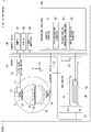
- FIG. 1 is a configuration diagram of an X-ray CT apparatus 1 according to an embodiment.
- the X-ray CT device 1 includes, for example, a gantry 10, a bed device 30, and a console device 40.
- FIG. 1 shows both a view of the gantry 10 from a Z-axis direction and a view from an X-axis direction for convenience of description, there is one gantry 10 in reality.
- a rotation shaft of a rotary frame 17 in a non-tilt state or the longitudinal direction of a top plate 33 of the bed device 30 is defined as the Z-axis direction
- an axis orthogonal to the Z-axis direction and horizontal to the floor surface is defined as the X-axis direction
- a direction orthogonal to the Z-axis direction and perpendicular to the floor surface is defined as a Y-axis direction.
- the X-ray CT apparatus 1 captures a contrast-enhanced CT image for performing imaging examination.
- the gantry 10 includes, for example, an X-ray tube 11, a wedge 12, a collimator 13, an X-ray high voltage device 14, an X-ray detector 15, a data acquisition system (hereinafter, DAS) 16, the rotary frame 17, and a control device 18.
- DAS data acquisition system
- the X-ray tube 11 generates X-rays by radiating thermions from a cathode (filament) toward an anode (target) when a high voltage from the X-ray high voltage device 14 is applied thereto.
- the X-ray tube 11 includes a vacuum tube.
- the X-ray tube 11 is a rotating anode type X-ray tube that generates X-rays by radiating thermions to a rotating anode.
- the wedge 12 is a filter for adjusting an X-ray dose radiated from the X-ray tube 11 to a subject P that is an imaging examination target.
- the wedge 12 attenuates X-rays passing therethrough such that the distribution of the X-ray dose applied to the subject P from the X-ray tube 11 becomes a predetermined distribution.
- the wedge 12 is also called a wedge filter or a bow-tie filter.
- the wedge 12 is made by processing aluminum so as to have a predetermined target angle and a predetermined thickness, for example.
- the collimator 13 is a mechanism for narrowing the radiation range of X-rays that have passed through the wedge 12.
- the collimator 13 narrows the radiation range of X-rays by forming a slit, for example, according to combination of a plurality of lead plates.
- the collimator 13 may be called an X-ray diaphragm.
- a narrowing range of the collimator 13 may be mechanically driven.
- the X-ray high voltage device 14 includes, for example, a high voltage generation device and an X-ray control device.
- the high voltage generation device has an electric circuit including a transformer, a rectifier, and the like and generates a high voltage applied to the X-ray tube 11.
- the X-ray control device controls an output voltage of the high voltage generation device according to the X-ray dose to be generated in the X-ray tube 11.
- the high voltage generation device may boost the voltage by the transformer described above or boost the voltage by an inverter.
- the X-ray high voltage device 14 may be provided on the rotary frame 17 or may be provided on the side of a fixed frame (not shown) of the gantry 10.
- the X-ray detector 15 detects the intensity of X-rays generated by the X-ray tube 11, passed through the subject P and incident thereon.
- the X-ray detector 15 outputs an electrical signal (which may be an optical signal or the like) depending on the intensity of the detected X-rays to the DAS 16.
- the X-ray detector 15 is, for example, a so-called photon counting detector that counts photons to measure X-rays.
- the X-ray detector 15 may be a scintillator.
- the X-ray detector 15 is an example of a radiation detector. The detailed configuration of the X-ray detector 15 will be described later.
- the DAS 16 includes, for example, an amplifier, an integrator, and an A/D converter.
- the amplifier performs amplification processing on an electrical signal output from each X-ray detection element of the X-ray detector 15.
- the integrator integrates the amplified electrical signal over a view period.
- the A/D converter converts an electrical signal indicating the integration result into a digital signal.
- the DAS 16 outputs detection data based on the digital signal to the console device 40.
- the rotary frame 17 is an annular rotating member that rotates the X-ray tube 11, the wedge 12, the collimator 13, and the X-ray detector 15 while holding them facing each other.
- the rotary frame 17 is rotatably supported by the fixed frame around the subject P introduced inside.
- the rotary frame 17 further supports the DAS 16.
- the detection data output from the DAS 16 is transmitted from a transmitter having light-emitting diodes (LEDs) provided in the rotary frame 17 to a receiver having photodiodes provided in a non-rotating part (for example, the fixed frame) of the gantry 10 according to optical communication and transferred to the console device 40 by the receiver.
- LEDs light-emitting diodes
- a method of transmitting the detection data from the rotary frame 17 to the non-rotating part is not limited to the above-mentioned method using optical communication, and any non-contact transmission method may be adopted.
- the rotary frame 17 is not limited to an annular member as long as it can support and rotate the X-ray tube 11 and the like and may be a member such as an arm.
- the X-ray CT apparatus 1 may be, for example, a rotate/rotate-type X-ray CT apparatus (third-generation CT) in which both the X-ray tube 11 and the X-ray detector 15 are supported by the rotary frame 17 and rotate around the subject P
- the X-ray CT apparatus 1 is not limited to this and may be a stationary/rotate-type X-ray CT apparatus (fourth-generation CT) in which a plurality of X-ray detection elements arranged in an annular shape are fixed to a fixed frame and the X-ray tube 11 rotates around the subject P.
- the control device 18 includes, for example, processing circuitry having a processor such as a central processing unit (CPU) and a drive mechanism including a motor, an actuator, and the like.
- the processing circuitry realizes these functions by, for example, a hardware processor executing a program stored in a storage device (storage circuit).
- the hardware processor means, for example, a circuit (circuitry) such as a central processing unit (CPU), a graphics processing unit (GPU), an application specific integrated circuit (ASIC), a programmable logic device (for example, a simple programmable logic device (SPLD) or a complex programmable logic device (CPLD)), and a field programmable gate array (FPGA).
- the program may be configured to be directly embedded in the circuit of the hardware processor instead of being stored in a storage device.
- the hardware processor realizes functions by reading and executing the program embedded in the circuit.
- the hardware processor is not limited to a configuration as a single circuit and may be configured as one hardware processor by combining a plurality of independent circuits to realize respective functions.
- the storage device may be a non-transitory (hardware) storage medium. Further, a plurality of components may be integrated into one hardware processor to realize respective functions.
- the control device 18 rotates the rotary frame 17, tilts the gantry of the gantry 10, moves the top plate 33 of the bed device 30 according to vertical movement, or the like, and causes X-rays to be radiated (allow exposure) from the X-ray tube 11, for example.
- the control device 18 may be provided in the gantry 10 or the console device 40.
- the bed device 30 is a device on which the subject P to be scanned is placed and introduced into the rotary frame 17 of the gantry 10.
- the bed device 30 includes, for example, a base 31, a bed driving device 32, the top plate 33, and a support frame 34.
- the base 31 includes a housing that movably supports the support frame 34 in the vertical direction (Y-axis direction).
- the bed driving device 32 includes a motor and an actuator.
- the bed driving device 32 moves the top plate 33 on which the subject P is placed along the support frame 34 in the longitudinal direction (Z-axis direction) of the top plate 33.
- the top plate 33 is a plate-shaped member on which the subject P is placed.
- the console device 40 includes, for example, a memory 41, a display 42, an input interface 43, and processing circuitry 50.
- the console device 40 will be described as a separate body from the gantry 10, but the gantry 10 may include a part or all of components of the console device 40.
- the memory 41 is realized by, for example, a semiconductor memory element such as a random access memory (RAM) and a flash memory, a hard disk, an optical disc, or the like.
- the memory 41 stores, for example, detection data, projection data, reconstructed image data, CT image data, and the like. Such data may be stored in an external memory with which the X-ray CT apparatus 1 can communicate instead of the memory 41 (or in addition to the memory 41).
- the external memory is controlled by, for example, a cloud server that manages the external memory upon reception of a read/write request by the cloud server.
- the display 42 displays various types of information.
- the display 42 displays a medical image (CT image) generated by the processing circuitry, a graphical user interface (GUI) image through which various operations by an operator such as a doctor or a technician are received, and the like.
- CT image medical image
- GUI graphical user interface
- the display 42 is, for example, a liquid crystal display, a cathode ray tube (CRT), an organic electroluminescence (EL) display, or the like.
- the display 42 may be provided on the gantry 10.
- the display 42 may be a desktop type or a display device (for example, a tablet terminal) capable of wirelessly communicating with the main body of the console device 40.
- the input interface 43 receives various input operations of the operator and outputs an electrical signal indicating details of the received input operations to the processing circuitry 50.
- the input interface 43 receives input operations such as collection conditions at the time of collecting detection data or projection data, reconstruction conditions at the time of reconstructing a CT image, and image processing conditions at the time of generating a post-processed image from a CT image.
- the input interface 43 is realized by, for example, a mouse, a keyboard, a touch panel, a drag ball, a switch, a button, a joystick, a camera, an infrared sensor, a microphone, or the like.
- the input interface 43 may be realized by a display device (for example, a tablet terminal) capable of wirelessly communicating with the main body of the console device 40.
- the input interface is not limited to the one provided with physical operation parts such as a mouse and a keyboard.
- examples of the input interface also include electrical signal processing circuitry that receives an electrical signal corresponding to an input operation from an external input apparatus provided separately from the device and outputs the electrical signal to the control circuit.
- the processing circuitry 50 controls the overall operation of the X-ray CT apparatus 1.
- the processing circuitry 50 includes, for example, a control function 51, a pre-processing function 52, a reconstruction processing function 53, and an image processing function 54.
- the processing circuitry 50 realizes these functions by, for example, a hardware processor executing a program stored in a storage device (storage circuit).
- the hardware processor means, for example, a circuit such as a CPU, a GPU, an application specific integrated circuit, a programmable logic device or a complex programmable logic device, and a field programmable gate array.
- the program may be configured to be directly embedded in the circuit of the hardware processor instead of being stored in the storage device.
- the hardware processor is not limited to a configuration as a single circuit and may be configured as one hardware processor by combining a plurality of independent circuits to realize respective functions.
- the storage device may be a non-transitory (hardware) storage medium. Further, a plurality of components may be integrated into one hardware processor to realize respective functions.
- Each component of the console device 40 or the processing circuitry 50 may be decentralized and realized by a plurality of hardware circuits.
- the processing circuitry 50 may be realized by a processing device capable of communicating with the console device 40 instead of being a component included in the console device 40.
- the processing device is, for example, a workstation connected to one X-ray CT apparatus or a device (for example, a cloud server) connected to a plurality of X-ray CT apparatuses and collectively executing the same processing as that of the processing circuitry 50 which will be described below.
- Each function included in the processing circuitry 50 may be distributed to a plurality of circuits or may be made available by activating application software stored in the memory 41.
- the control function 51 controls various functions of the processing circuitry 50 on the basis of input operations received by the input interface 43.
- the pre-processing function 52 performs pre-processing such as logarithmic conversion processing, offset correction processing, inter-channel sensitivity correction processing, and beam hardening correction on detection data output from DAS 16 to generate projection data and stores the generated projection data in the memory 41.
- the reconstruction processing function 53 performs reconstruction processing on the projection data generated by the pre-processing function 52 by a filter correction back projection method, a successive approximation reconstruction method, or the like to generate CT image data and stores the generated CT image data in the memory 41.
- the image processing function 54 converts the CT image data into three-dimensional image data or cross-sectional image data with an arbitrary cross section by a known method on the basis of an input operation received by the input interface 43. Conversion into the three-dimensional image data may be performed by the pre-processing function 52.
- the X-ray detector 15 is provided by arranging a plurality of X-ray detector units 15A side by side.
- FIG. 2 is an enlarged view showing a part of the X-ray detector unit 15A.
- the X-ray detector unit 15A includes, for example, a plurality of radiation detector modules (hereinafter, detector modules) 100 and a positioning plate 200.
- the plurality of detector modules 100 are arranged in a row and fixed to the positioning plate 200.
- the plurality of detector modules 100 are positioned such that their positions relative to each other can be adjusted.
- the detector modules 100 are an X-ray detection element array.
- Each detector module 100 includes, for example, a first electrode 61, a detection element 62, a second electrode 63, a substrate layer 64, and a mounting member 65.
- the side of the detector module 100 on which the first electrode 61 is provided may be referred to as an upper side and the side on which the second electrode 63 is provided may be referred to as a lower side.
- the first electrode 61 is provided on the surface side (upper side) of the detection element 62.
- the first electrode 61 is a high voltage (HV) electrode having a higher potential than that of the second electrode 63.
- the first electrode 61 is formed, for example, by depositing a metal material on the surface of the detection element 62.
- the first electrode 61 may be formed by a method other than vapor deposition.
- the detection element 62 is formed of, for example, CdTe or CZT.
- the detection element 62 detects radiation incident from an incident surface on the surface side of the detector module 100.
- the plurality of detector modules 100 are provided, for example, by being linearly arranged on the positioning plate 200 having a substantially rectangular parallelepiped outer shape.
- the detection element 62 is an example of a radiation detection element.
- the second electrode 63 is provided on the back surface of the detection element 62.
- the second electrode 63 is provided such that it faces the first electrode 61 with the detection element 62 interposed therebetween.
- the second electrode 63 is a low voltage (LV) electrode.
- the substrate layer 64 is provided on the back surface side of the second electrode 63.
- the substrate layer 64 supports the first electrode 61, the detection element 62, and the second electrode 63.
- the substrate layer 64 includes, for example, a support substrate. Electrical elements such as IC chips are attached to the support substrate. The electrical elements are connected through, for example, a wiring cable.
- the mounting member 65 is housed in a plurality of positioning holes 71 formed in the positioning plate 200 and is fixed to the positioning plate by a screw 72.
- the substrate layer 64 is fixed to the mounting member 65 with a screw or the like that is not shown. By fixing the substrate layer 64 to the mounting member 65, the detector module 100 is fixed to the positioning plate 200.
- FIG. 3 is a diagram showing the surface of the detection element 62 when the through hole 61A is viewed from above.
- a mark 66 is provided on the exposed portion on the surface of the detection element 62.
- the mark 66 includes, for example, a portion formed by covering the entire surface of the detection element 62 seen through the through hole 61A with the same material as the first electrode 61 and hollowing out the central portion thereof.
- the mark 66 is formed by masking the portion of the surface of the detection element 62 seen through the through hole 61A, on which the mark 66 will be formed, at the time of vapor-depositing the metal to form the first electrode 61.
- the mark 66 has a bordering portion 62A that borders the mark 66, formed on the surface of the detection element 62 seen through the through hole 61A.
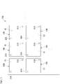
- FIG. 4 is a diagram showing a state in which the detector module 100 is viewed from above.
- the detector module 100 is provided with, for example, a plurality of second electrodes 63.
- the second electrodes 63 all have substantially the same rectangular shape when viewed from above.
- the plurality of second electrodes 63 are arranged in a matrix.
- One pixel is configured for one second electrode 63.
- Two through holes 61A are formed in the first electrode 61 such that they face corners where four second electrodes 63 at diagonal positions of the first electrode 61 among the plurality of second electrodes 63 arranged in a matrix face each other.
- the mark 66 is provided on both portions of the surface of the detection element 62 seen through the two through holes 61A.
- the mark 66 is provided at a plurality of places (two places in the first embodiment) on the surface of the detection element 62.
- the through holes 61A are provided only at positions where the mark 66 can be visually recognized from the incident surface side.
- the through holes 61A may be provided at positions other than the positions where the mark 66 can be visually recognized from the incident surface side.
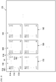
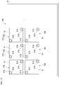
- FIG. 5 is a view of the X-ray detector unit 15A when viewed from above.
- the plurality of detector modules 100 are arranged side by side in the X-ray detector unit 15A.
- Two through holes 61A are formed in each of the plurality of detector modules 100, and the mark 66 (refer to FIG. 3 ) is provided at positions seen through the through holes 61A.
- the adjacent detector modules 100 are positioned with respect to each other.
- the mark 66 is provided on the basis of the positions of the second electrodes 63.
- the mark 66 is provided, for example, to position the plurality of detector modules 100 such that pixels of adjacent detector modules 100 are arranged in an orderly manner. Since the pixels in the detector modules 100 are based on the positions and range of the second electrodes 63, the mark 66 is used to align the second electrodes 63 with the second electrodes 63 in another adjacent detector module 100.
- the substrate layer 64 is manufactured first, and the second electrode 63 is manufactured on the surface of the substrate layer 64 by, for example, vapor deposition. Subsequently, the detection element 62 is formed on the surface of the second electrode 63.
- the first electrode 61 is formed by depositing a metal to be the first electrode 61 on the surface of the detection element 62. At the time of depositing the metal to be the first electrode 61, portions to be the through holes 61A and portions to be the marks 66 are masked. In this manner, the marks 66 bordered by the bordering portions 62A formed of the same material as the first electrode 61 is formed.
- the layer of the first electrode 61 may be formed after formation of the layer of the bordering portions 62A and the marks 66.
- the through holes 61A may be formed by depositing a metal to be the first electrode 61 on the overall surface of the detection element 62 and then performing etching preprocess or the like.
- FIG. 6 is a flowchart showing an example of a manufacturing procedure of the X-ray detector unit 15A.
- the assembled detector modules 100 are grasped by, for example, a robot hand and disposed on the positioning plate 200 (step S101). In this state, the detector modules 100 are not yet fixed to the positioning plate 200.
- the detector modules 100 are imaged by a camera from above (step S103), and the camera transmits the captured image to a control device that is not shown.
- the control device analyzes the transmitted image and sets the position of each detector module 100 on the basis of the positions of the marks 66 provided on each of the plurality of detector modules 100 in the image.
- the control device controls the robot hand on the basis of the set position of each detector module 100 and finely adjusts the positions of adjacent detector modules 100 (step S105).
- the detector modules 100 are additionally imaged with the camera from above and the positions of the detector modules 100 are adjusted on the basis of the marks 66 provided on each of the plurality of detector modules 100 in the image.
- the marks 66 of adjacent detector modules 100 are aligned, and further, the second electrodes 63 are aligned.
- the control device determines whether or not position adjustment of the detector modules 100 is completed (step S107). If it is determined that position adjustment of the detector modules 100 is not completed, the procedure returns to step S105 and the positions of the detector modules 100 are finely adjusted.
- the detector modules 100 are fixed to the positioning plate 200 by fixing the detector modules 100 to the mounting member 65 and fixing the mounting member 65 to the positioning plate 200 by the screw 72 (step S109). In this manner, manufacturing of the X-ray detector unit 15A is completed.
- the mark 66 for aligning pixels between adjacent detector module 100 is provided on the detection element 62.
- the first electrode 61 is provided with the through hole 61A that allows the mark 66 provided on the detection element 62 to be visually recognizable. Accordingly, positioning is performed while viewing the mark 66, and thus the accuracy of positioning of the detector modules 100 can be improved.
- FIG. 7 is a view of the detector module 100 of the second embodiment when viewed from above.
- the detector module 100 of the second embodiment includes a plurality of second electrodes 63 arranged in a matrix as in the first embodiment.
- Through holes 61A are provided at positions of the first electrode 61 corresponding to corners where four second electrodes 63 face each other in each of the plurality of second electrodes 63. Accordingly, a larger number of through holes 61A than in the first embodiment is provided.
- Marks 66 are provided on the surface of the detection element 62 seen through two through holes 61A provided at the corners where the four second electrodes 63 at diagonal positions of the first electrode 61 face each other among the large number of through holes 61A. Accordingly, the first electrode 61 is provided with a larger number of through holes 61A than the number of marks 66.
- the large number of through holes 61A provided in the first electrode 61 are provided corresponding to the positions of the second electrodes 63. Accordingly, the plurality of through holes 61A are arranged symmetrically on the surface of the first electrode 61, so to speak, arranged and formed in a well-balanced manner. Further, since the through holes 61A are provided at the corners where the four second electrodes 63 face each other, the area of a portion of the first electrode 61 facing the second electrodes 63 is not so small.
- FIG. 8 is a view of the X-ray detector unit 15A of the second embodiment when viewed from above.
- the plurality of detector modules 100 are each provided with marks 66 (refer to FIG. 2 ) at positions seen through the two through holes 61A at diagonal positions of the first electrode 61. By aligning the positions of the marks 66 seen through the through holes 61A between adjacent detector modules 100, the adjacent detector modules 100 are positioned with respect to each other.
- the detector module 100 of the second embodiment has the same effect as that of the detector module 100 of the first embodiment. Further, in the detector module 100 of the second embodiment, the first electrode 61 is provided with a large number of through holes 61A corresponding to the positions of the second electrodes 63. Accordingly, a voltage is evenly applied to the second electrodes 63, in other words, evenly applied to the pixels in the first electrode 61, and thus the detection accuracy of the detection element 62 can be improved.
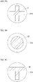
- the mark 66 has a substantially cross shape but may have other shapes.
- FIG. 9A to FIG. 9C are views all showing other examples of marks.
- a mark 81 is formed of the same material as the first electrode 61 or a different material on the surface of the detection element seen through the through hole 61A.
- the mark 81 may be formed on the surface of the detection element 62 before the first electrode 61 is formed.
- the mark 81 may be formed by masking a portion excluding the portion to be the mark 81, or the mark 81 may be formed through etching processing.
- a circular mark 82 may be formed on the surface of the detection element seen through the through hole 61A.
- a substantially T-shaped mark 83 may be formed on the surface of the detection element seen through the through hole 61A.
- the mark 66 is provided on the surface of the detection element 62.
- the mark 66 may be provided on the surface of the first electrode 61.
- the mark 66 may be provided at the same time when the first electrode 61 is formed by masking the place where the mark 66 will be provided and depositing a metal on the surface of the detection element 62.
- the mark 66 may be formed by performing etching processing after formation of the first electrode 61.
- the mark 66 may be provided on both the surface of the first electrode 61 and the surface of the detection element 62.
- a single mark 66 may be provided or three or more marks 66 may be provided.
- the mark 66 is provided at the same position between adjacent detector modules 100, the mark 66 may be provided at different positions between adjacent detector modules 100.
- the mark 66 may be formed of a material other than the same material as the first electrode 61.
- the mark 66 may be provided by applying a paint or the like on the surface of the detection element 62 or the first electrode 61.
- the through hole 61A for allowing the mark 66 to be visually recognizable from the incident surface side is provided in the first electrode 61 in the first embodiment
- a through hole that allows the mark 66 to be visually recognizable from the incident surface side is also provided in an electrode film provided on the upper side of the first electrode 61 in the third embodiment.
- FIG. 10 is an enlarged view showing a part of an X-ray detector unit 15B according to the third embodiment.
- the X-ray detector unit 15B shown in FIG. 10 includes an electrode film 67 additionally provided on the X-ray detector unit 15A shown in FIG. 2 .
- the electrode film 67 is provided on the upper side of the first electrode 61 of each detector module 100 included in the X-ray detector unit 15A.
- the electrode film 67 is conductive and has a film shape.
- the electrode film 67 uniformly supplies a voltage supplied from a voltage source (not shown) to the first electrode 61 of each detector module 100.
- Through holes 67A are formed in the electrode film 67. At the portions where the through holes 67A are formed, parts of the surface of the detection element 62 are exposed through the through holes 61A of the first electrode 61. When the through holes 67A are viewed from above the electrode film 67, the exposed portions on the surface of the detection element 62 can be visually recognized. For example, the mark 66 as shown in FIG. 3 is provided on the exposed portions on the surface of the detection element 62.
- FIG. 11 is a view of the X-ray detector unit 15B according to the third embodiment when viewed from above.
- a plurality of detector modules 100 are arranged side by side in the X-ray detector unit 15B.
- two through holes 61A are formed in the first electrode 61 and the marks 66 (refer to FIG. 3 ) are provided at positions seen through the through holes 61A.
- through holes 67A are provided at positions corresponding to the marks 66 of the electrode film 67.
- the marks 66 on the surface of the detection element 62 can be visually recognized through the through holes 61A of the first electrode 61.
- marks 66 for aligning pixels between adjacent detector module 100 are provided on the detection element 62.
- the first electrode 61 is provided with the through holes 61A that allow the marks 66 provided on the detection element 62 to be visually recognizable
- the electrode film 67 is provided with through holes 67A that allow the marks 66 provided on the detection element 62 to be visually recognizable via the through holes 61A. Accordingly, positioning is performed while viewing the marks 66, and thus the accuracy of positioning of the detector module 100 can be improved.
- FIG. 12 is a diagram showing a state in which processing of estimating the position of each pixel is performed using a pencil beam PB according to the fourth embodiment.
- an X-ray source 300 radiates the pencil beam PB (X-ray) to the detector module 100 from above the first electrode 61 of the detector module 100.
- radiation by the X-ray source 300 is performed while moving the radiation position of the pencil beam PB in the detector module 100 in a predetermined direction (for example, a direction D).
- radiation by the X-ray source 300 may be performed while moving the radiation position of the pencil beam PB in the detector module 100 in a direction orthogonal to the direction D on the upper side surface of the first electrode 61.
- the pencil beam PB has, for example, a beam size equal to or less than the size of each pixel.
- the pencil beam PB may have a beam size larger than the size of each pixel.
- the positions of pixels are estimated by observing change in an electrical signal output from the detector module 100, accompanied by change in the radiation position of the pencil beam PB.
- an output value (electrical signal) of the detector module 100 shows a peak PK when radiation positions of the pencil beam PB are positions PT1, PT2, and PT3.
- the positions PT1, PT2, and PT3 at which the output value indicates the peak PK are center positions of pixels (center positions of the second electrode 63).
- Such estimation processing may be performed, for example, in the processing circuitry 50 of the console device 40, and the estimation result may be output to the display 42.
- the position of each pixel is estimated by using a pencil beam in order to align pixels between adjacent detector modules 100. Accordingly, the accuracy of positioning of the detector module 100 can be improved.
- the radiation detector module by including a radiation detection element that detects radiation incident from an incident surface, a first electrode provided on an incident surface side of the radiation detection element, a second electrode provided to face the first electrode having the radiation detection element interposed therebetween, and a mark provided on at least one of the incident surface of the radiation detection element and the first electrode.
Landscapes
- Health & Medical Sciences (AREA)
- Life Sciences & Earth Sciences (AREA)
- Engineering & Computer Science (AREA)
- Physics & Mathematics (AREA)
- Medical Informatics (AREA)
- Molecular Biology (AREA)
- High Energy & Nuclear Physics (AREA)
- Pathology (AREA)
- Nuclear Medicine, Radiotherapy & Molecular Imaging (AREA)
- General Health & Medical Sciences (AREA)
- Radiology & Medical Imaging (AREA)
- General Physics & Mathematics (AREA)
- Veterinary Medicine (AREA)
- Public Health (AREA)
- Animal Behavior & Ethology (AREA)
- Heart & Thoracic Surgery (AREA)
- Biomedical Technology (AREA)
- Optics & Photonics (AREA)
- Surgery (AREA)
- Biophysics (AREA)
- Theoretical Computer Science (AREA)
- Spectroscopy & Molecular Physics (AREA)
- Pulmonology (AREA)
- Mathematical Physics (AREA)
- Chemical & Material Sciences (AREA)
- Immunology (AREA)
- Biochemistry (AREA)
- Analytical Chemistry (AREA)
- Apparatus For Radiation Diagnosis (AREA)
- Measurement Of Radiation (AREA)
Abstract
Description
- Embodiments disclosed in the present description and drawings relate to a radiation detector module, a radiation detector, and an X-ray CT apparatus.
- A plurality of radiation detector modules are arranged side by side in a radiation detector. When radiation is detected by a plurality of radiation detector modules arranged side by side, the accuracy of positioning of the radiation detector modules has a great influence on the detection accuracy of the radiation detector. Positioning of radiation detector modules has been performed, for example, on the basis of pins provided on a mounting part of the radiation detector modules.
- However, it is difficult to improve the accuracy of positioning based on the pins. In particular, the detection accuracy of a radiation detector is greatly affected by the relative positional relationship between radiation detector modules arranged side by side. However, since positioning based on the pins does not directly adjust the positional relationship between radiation detector modules, it is difficult to improve the positioning accuracy of the radiation detector modules.
- A problem to be solved by the embodiments disclosed in the present description and the drawings is to improve the positioning accuracy of radiation detector modules. However, the problems to be solved by the embodiments disclosed in the present description and the drawings are not limited to the above problem. It is also possible to regard a problem corresponding to each effect according to each configuration illustrated in an embodiment which will be described later as another problem.
- A radiation detector module of an embodiment includes a radiation detector, a first electrode, a second electrode, and a mark. The radiation detector includes an incident surface and is configured to detect radiation incident from the incident surface. The first electrode is provided on the side of the incident surface of the radiation detector. The second electrode is provided to face the first electrode through the radiation detector. The mark is provided on at least one of the incident surface of the radiation detector and the first electrode.
- (1) A radiation detector module including:
- a radiation detection element that includes an incident surface and is configured to detect radiation incident from the incident surface;
- a first electrode provided on a side of the incident surface of the radiation detection element;
- a second electrode provided to face the first electrode through the radiation detection element; and
- a mark provided on at least one of the incident surface of the radiation detection element and the first electrode.
- (2) The mark may be provided based on the position of the second electrode.
- (3) The mark may be provided on the incident surface of the radiation detection element, and a through hole configured to allow the mark to be visually recognizable from the side of the incident surface may be provided on the first electrode.
- (4) The through hole may be provided only at a position where the mark is visually recognizable from the side of the incident surface.
- (5) The through hole may be provided at a plurality of positions including a position where the mark is visually recognizable from the side of the incident surface.
- (6) A plurality of marks may be included.
- (7) The mark may include the same material as the first electrode.
- (8) The first electrode may be provided by depositing a material on the radiation detection element, and the mark may be provided by being masked when the first electrode is formed.
- (9) The radiation detector module may be provided in a radiation detector including a plurality of radiation detector modules, and the mark may be used for positioning the second electrode and another second electrode in another adjacent radiation detector module.
- (10) An electrode film provided on the side of the incident surface of the first electrode and supplying a voltage to the first electrode may be further included, and a through hole configured to allow the mark to be visually recognizable from the side of the incident surface may be provided in the electrode film.
- (11) A radiation detector including the aforementioned radiation detector module.
- (12) An X-ray CT apparatus including the radiation detector, wherein the radiation is X-rays.
- (13) The through hole provided in the electrode film may be configured to allow mark to be visually recognizable from the side of the incident surface through the through hole provided in the first electrode.
- (14) The mark and the through hole of the first electrode may be provided at positions corresponding to corners where four second electrodes among a plurality of second electrodes arranged in a matrix face each other.
- (15) The first electrode may be provided by depositing a material on the radiation detection element, and the mark may be provided by being masked when the first electrode is formed to form a bordering portion for bordering the mark.
- (16) The mark may have any of a cross shape, a circular shape, and a T-shape.
-
-
FIG. 1 is a configuration diagram of an X-ray CT apparatus 1 according to a first embodiment. -
FIG. 2 is an enlarged view showing a part of anX-ray detector unit 15A according to the first embodiment. -
FIG. 3 is a diagram showing a surface of adetection element 62 when athrough hole 61A according to the first embodiment is viewed from above. -
FIG. 4 is a diagram showing a state in which adetector module 100 according to the first embodiment is viewed from above. -
FIG. 5 is a diagram of theX-ray detector unit 15A according to the first embodiment when viewed from above. -
FIG. 6 is a flowchart showing a process of manufacturing theX-ray detector unit 15A according to the first embodiment. -
FIG. 7 is a diagram of adetector module 100 of a second embodiment when viewed from above. -
FIG. 8 is a diagram of anX-ray detector unit 15A of the second embodiment when viewed from above. -
FIG. 9A is a diagram showing another example of a mark. -
FIG. 9B is a diagram showing another example of the mark. -
FIG. 9C is a diagram showing another example of the mark. -
FIG. 10 is an enlarged view showing a part of anX-ray detector unit 15B according to a third embodiment. -
FIG. 11 is a diagram of theX-ray detector unit 15B according to the third embodiment when viewed from above. -
FIG. 12 is a diagram showing a state in which processing of estimating the position of each pixel is performed using a pencil beam PB according to a fourth embodiment. - Hereinafter, a radiation detector module, a radiation detector, and an X-ray CT apparatus of embodiments will be described with reference to the drawings.
-
FIG. 1 is a configuration diagram of an X-ray CT apparatus 1 according to an embodiment. The X-ray CT device 1 includes, for example, agantry 10, abed device 30, and aconsole device 40. AlthoughFIG. 1 shows both a view of thegantry 10 from a Z-axis direction and a view from an X-axis direction for convenience of description, there is onegantry 10 in reality. In the embodiment, a rotation shaft of arotary frame 17 in a non-tilt state or the longitudinal direction of atop plate 33 of thebed device 30 is defined as the Z-axis direction, an axis orthogonal to the Z-axis direction and horizontal to the floor surface is defined as the X-axis direction, and a direction orthogonal to the Z-axis direction and perpendicular to the floor surface is defined as a Y-axis direction. The X-ray CT apparatus 1 captures a contrast-enhanced CT image for performing imaging examination. - The
gantry 10 includes, for example, anX-ray tube 11, awedge 12, acollimator 13, an X-rayhigh voltage device 14, anX-ray detector 15, a data acquisition system (hereinafter, DAS) 16, therotary frame 17, and acontrol device 18. - The
X-ray tube 11 generates X-rays by radiating thermions from a cathode (filament) toward an anode (target) when a high voltage from the X-rayhigh voltage device 14 is applied thereto. TheX-ray tube 11 includes a vacuum tube. For example, theX-ray tube 11 is a rotating anode type X-ray tube that generates X-rays by radiating thermions to a rotating anode. - The
wedge 12 is a filter for adjusting an X-ray dose radiated from theX-ray tube 11 to a subject P that is an imaging examination target. Thewedge 12 attenuates X-rays passing therethrough such that the distribution of the X-ray dose applied to the subject P from theX-ray tube 11 becomes a predetermined distribution. Thewedge 12 is also called a wedge filter or a bow-tie filter. Thewedge 12 is made by processing aluminum so as to have a predetermined target angle and a predetermined thickness, for example. - The
collimator 13 is a mechanism for narrowing the radiation range of X-rays that have passed through thewedge 12. Thecollimator 13 narrows the radiation range of X-rays by forming a slit, for example, according to combination of a plurality of lead plates. Thecollimator 13 may be called an X-ray diaphragm. A narrowing range of thecollimator 13 may be mechanically driven. - The X-ray
high voltage device 14 includes, for example, a high voltage generation device and an X-ray control device. The high voltage generation device has an electric circuit including a transformer, a rectifier, and the like and generates a high voltage applied to theX-ray tube 11. The X-ray control device controls an output voltage of the high voltage generation device according to the X-ray dose to be generated in theX-ray tube 11. The high voltage generation device may boost the voltage by the transformer described above or boost the voltage by an inverter. The X-rayhigh voltage device 14 may be provided on therotary frame 17 or may be provided on the side of a fixed frame (not shown) of thegantry 10. - The
X-ray detector 15 detects the intensity of X-rays generated by theX-ray tube 11, passed through the subject P and incident thereon. TheX-ray detector 15 outputs an electrical signal (which may be an optical signal or the like) depending on the intensity of the detected X-rays to theDAS 16. TheX-ray detector 15 is, for example, a so-called photon counting detector that counts photons to measure X-rays. TheX-ray detector 15 may be a scintillator. TheX-ray detector 15 is an example of a radiation detector. The detailed configuration of theX-ray detector 15 will be described later. - The
DAS 16 includes, for example, an amplifier, an integrator, and an A/D converter. The amplifier performs amplification processing on an electrical signal output from each X-ray detection element of theX-ray detector 15. The integrator integrates the amplified electrical signal over a view period. The A/D converter converts an electrical signal indicating the integration result into a digital signal. TheDAS 16 outputs detection data based on the digital signal to theconsole device 40. - The
rotary frame 17 is an annular rotating member that rotates theX-ray tube 11, thewedge 12, thecollimator 13, and theX-ray detector 15 while holding them facing each other. Therotary frame 17 is rotatably supported by the fixed frame around the subject P introduced inside. Therotary frame 17 further supports theDAS 16. The detection data output from theDAS 16 is transmitted from a transmitter having light-emitting diodes (LEDs) provided in therotary frame 17 to a receiver having photodiodes provided in a non-rotating part (for example, the fixed frame) of thegantry 10 according to optical communication and transferred to theconsole device 40 by the receiver. A method of transmitting the detection data from therotary frame 17 to the non-rotating part is not limited to the above-mentioned method using optical communication, and any non-contact transmission method may be adopted. Therotary frame 17 is not limited to an annular member as long as it can support and rotate theX-ray tube 11 and the like and may be a member such as an arm. - Although the X-ray CT apparatus 1 may be, for example, a rotate/rotate-type X-ray CT apparatus (third-generation CT) in which both the
X-ray tube 11 and theX-ray detector 15 are supported by therotary frame 17 and rotate around the subject P, the X-ray CT apparatus 1 is not limited to this and may be a stationary/rotate-type X-ray CT apparatus (fourth-generation CT) in which a plurality of X-ray detection elements arranged in an annular shape are fixed to a fixed frame and theX-ray tube 11 rotates around the subject P. - The
control device 18 includes, for example, processing circuitry having a processor such as a central processing unit (CPU) and a drive mechanism including a motor, an actuator, and the like. The processing circuitry realizes these functions by, for example, a hardware processor executing a program stored in a storage device (storage circuit). - The hardware processor means, for example, a circuit (circuitry) such as a central processing unit (CPU), a graphics processing unit (GPU), an application specific integrated circuit (ASIC), a programmable logic device (for example, a simple programmable logic device (SPLD) or a complex programmable logic device (CPLD)), and a field programmable gate array (FPGA). The program may be configured to be directly embedded in the circuit of the hardware processor instead of being stored in a storage device. In this case, the hardware processor realizes functions by reading and executing the program embedded in the circuit. The hardware processor is not limited to a configuration as a single circuit and may be configured as one hardware processor by combining a plurality of independent circuits to realize respective functions. The storage device may be a non-transitory (hardware) storage medium. Further, a plurality of components may be integrated into one hardware processor to realize respective functions.
- The
control device 18 rotates therotary frame 17, tilts the gantry of thegantry 10, moves thetop plate 33 of thebed device 30 according to vertical movement, or the like, and causes X-rays to be radiated (allow exposure) from theX-ray tube 11, for example. Thecontrol device 18 may be provided in thegantry 10 or theconsole device 40. - The
bed device 30 is a device on which the subject P to be scanned is placed and introduced into therotary frame 17 of thegantry 10. Thebed device 30 includes, for example, abase 31, abed driving device 32, thetop plate 33, and a support frame 34. Thebase 31 includes a housing that movably supports the support frame 34 in the vertical direction (Y-axis direction). Thebed driving device 32 includes a motor and an actuator. Thebed driving device 32 moves thetop plate 33 on which the subject P is placed along the support frame 34 in the longitudinal direction (Z-axis direction) of thetop plate 33. Thetop plate 33 is a plate-shaped member on which the subject P is placed. - The
console device 40 includes, for example, amemory 41, adisplay 42, aninput interface 43, andprocessing circuitry 50. In the embodiment, theconsole device 40 will be described as a separate body from thegantry 10, but thegantry 10 may include a part or all of components of theconsole device 40. - The
memory 41 is realized by, for example, a semiconductor memory element such as a random access memory (RAM) and a flash memory, a hard disk, an optical disc, or the like. Thememory 41 stores, for example, detection data, projection data, reconstructed image data, CT image data, and the like. Such data may be stored in an external memory with which the X-ray CT apparatus 1 can communicate instead of the memory 41 (or in addition to the memory 41). The external memory is controlled by, for example, a cloud server that manages the external memory upon reception of a read/write request by the cloud server. - The
display 42 displays various types of information. For example, thedisplay 42 displays a medical image (CT image) generated by the processing circuitry, a graphical user interface (GUI) image through which various operations by an operator such as a doctor or a technician are received, and the like. Thedisplay 42 is, for example, a liquid crystal display, a cathode ray tube (CRT), an organic electroluminescence (EL) display, or the like. Thedisplay 42 may be provided on thegantry 10. Thedisplay 42 may be a desktop type or a display device (for example, a tablet terminal) capable of wirelessly communicating with the main body of theconsole device 40. - The
input interface 43 receives various input operations of the operator and outputs an electrical signal indicating details of the received input operations to theprocessing circuitry 50. For example, theinput interface 43 receives input operations such as collection conditions at the time of collecting detection data or projection data, reconstruction conditions at the time of reconstructing a CT image, and image processing conditions at the time of generating a post-processed image from a CT image. - The
input interface 43 is realized by, for example, a mouse, a keyboard, a touch panel, a drag ball, a switch, a button, a joystick, a camera, an infrared sensor, a microphone, or the like. Theinput interface 43 may be realized by a display device (for example, a tablet terminal) capable of wirelessly communicating with the main body of theconsole device 40. - In the present description, the input interface is not limited to the one provided with physical operation parts such as a mouse and a keyboard. For example, examples of the input interface also include electrical signal processing circuitry that receives an electrical signal corresponding to an input operation from an external input apparatus provided separately from the device and outputs the electrical signal to the control circuit.
- The
processing circuitry 50 controls the overall operation of the X-ray CT apparatus 1. Theprocessing circuitry 50 includes, for example, acontrol function 51, apre-processing function 52, areconstruction processing function 53, and animage processing function 54. Theprocessing circuitry 50 realizes these functions by, for example, a hardware processor executing a program stored in a storage device (storage circuit). - The hardware processor means, for example, a circuit such as a CPU, a GPU, an application specific integrated circuit, a programmable logic device or a complex programmable logic device, and a field programmable gate array. The program may be configured to be directly embedded in the circuit of the hardware processor instead of being stored in the storage device. The hardware processor is not limited to a configuration as a single circuit and may be configured as one hardware processor by combining a plurality of independent circuits to realize respective functions. The storage device may be a non-transitory (hardware) storage medium. Further, a plurality of components may be integrated into one hardware processor to realize respective functions.
- Each component of the
console device 40 or theprocessing circuitry 50 may be decentralized and realized by a plurality of hardware circuits. Theprocessing circuitry 50 may be realized by a processing device capable of communicating with theconsole device 40 instead of being a component included in theconsole device 40. The processing device is, for example, a workstation connected to one X-ray CT apparatus or a device (for example, a cloud server) connected to a plurality of X-ray CT apparatuses and collectively executing the same processing as that of theprocessing circuitry 50 which will be described below. Each function included in theprocessing circuitry 50 may be distributed to a plurality of circuits or may be made available by activating application software stored in thememory 41. - The
control function 51 controls various functions of theprocessing circuitry 50 on the basis of input operations received by theinput interface 43. Thepre-processing function 52 performs pre-processing such as logarithmic conversion processing, offset correction processing, inter-channel sensitivity correction processing, and beam hardening correction on detection data output fromDAS 16 to generate projection data and stores the generated projection data in thememory 41. - The
reconstruction processing function 53 performs reconstruction processing on the projection data generated by thepre-processing function 52 by a filter correction back projection method, a successive approximation reconstruction method, or the like to generate CT image data and stores the generated CT image data in thememory 41. - The
image processing function 54 converts the CT image data into three-dimensional image data or cross-sectional image data with an arbitrary cross section by a known method on the basis of an input operation received by theinput interface 43. Conversion into the three-dimensional image data may be performed by thepre-processing function 52. - Subsequently, the configuration of the
X-ray detector 15 will be described. TheX-ray detector 15 is provided by arranging a plurality ofX-ray detector units 15A side by side.FIG. 2 is an enlarged view showing a part of theX-ray detector unit 15A. TheX-ray detector unit 15A includes, for example, a plurality of radiation detector modules (hereinafter, detector modules) 100 and apositioning plate 200. The plurality ofdetector modules 100 are arranged in a row and fixed to thepositioning plate 200. The plurality ofdetector modules 100 are positioned such that their positions relative to each other can be adjusted. Thedetector modules 100 are an X-ray detection element array. - Each
detector module 100 includes, for example, afirst electrode 61, adetection element 62, asecond electrode 63, asubstrate layer 64, and a mountingmember 65. In the following description, the side of thedetector module 100 on which thefirst electrode 61 is provided may be referred to as an upper side and the side on which thesecond electrode 63 is provided may be referred to as a lower side. - The
first electrode 61 is provided on the surface side (upper side) of thedetection element 62. Thefirst electrode 61 is a high voltage (HV) electrode having a higher potential than that of thesecond electrode 63. Thefirst electrode 61 is formed, for example, by depositing a metal material on the surface of thedetection element 62. Thefirst electrode 61 may be formed by a method other than vapor deposition. - The
detection element 62 is formed of, for example, CdTe or CZT. Thedetection element 62 detects radiation incident from an incident surface on the surface side of thedetector module 100. The plurality ofdetector modules 100 are provided, for example, by being linearly arranged on thepositioning plate 200 having a substantially rectangular parallelepiped outer shape. Thedetection element 62 is an example of a radiation detection element. - The
second electrode 63 is provided on the back surface of thedetection element 62. Thesecond electrode 63 is provided such that it faces thefirst electrode 61 with thedetection element 62 interposed therebetween. Thesecond electrode 63 is a low voltage (LV) electrode. By energizing thefirst electrode 61 and thesecond electrode 63, radiation is detected by thedetection element 62. - The
substrate layer 64 is provided on the back surface side of thesecond electrode 63. Thesubstrate layer 64 supports thefirst electrode 61, thedetection element 62, and thesecond electrode 63. Thesubstrate layer 64 includes, for example, a support substrate. Electrical elements such as IC chips are attached to the support substrate. The electrical elements are connected through, for example, a wiring cable. - The mounting
member 65 is housed in a plurality of positioning holes 71 formed in thepositioning plate 200 and is fixed to the positioning plate by ascrew 72. Thesubstrate layer 64 is fixed to the mountingmember 65 with a screw or the like that is not shown. By fixing thesubstrate layer 64 to the mountingmember 65, thedetector module 100 is fixed to thepositioning plate 200. - Further, a through
hole 61A is formed in thefirst electrode 61. A part of the surface of thedetection element 62 is exposed at the portion where the throughhole 61A is formed. When the throughhole 61A is viewed from above thefirst electrode 61, the exposed portion on the surface of thedetection element 62 can be visually recognized.FIG. 3 is a diagram showing the surface of thedetection element 62 when the throughhole 61A is viewed from above. - A
mark 66 is provided on the exposed portion on the surface of thedetection element 62. Themark 66 includes, for example, a portion formed by covering the entire surface of thedetection element 62 seen through the throughhole 61A with the same material as thefirst electrode 61 and hollowing out the central portion thereof. Themark 66 is formed by masking the portion of the surface of thedetection element 62 seen through the throughhole 61A, on which themark 66 will be formed, at the time of vapor-depositing the metal to form thefirst electrode 61. Themark 66 has a borderingportion 62A that borders themark 66, formed on the surface of thedetection element 62 seen through the throughhole 61A. -
FIG. 4 is a diagram showing a state in which thedetector module 100 is viewed from above. Thedetector module 100 is provided with, for example, a plurality ofsecond electrodes 63. Thesecond electrodes 63 all have substantially the same rectangular shape when viewed from above. The plurality ofsecond electrodes 63 are arranged in a matrix. One pixel is configured for onesecond electrode 63. - Two through
holes 61A are formed in thefirst electrode 61 such that they face corners where foursecond electrodes 63 at diagonal positions of thefirst electrode 61 among the plurality ofsecond electrodes 63 arranged in a matrix face each other. Themark 66 is provided on both portions of the surface of thedetection element 62 seen through the two throughholes 61A. Themark 66 is provided at a plurality of places (two places in the first embodiment) on the surface of thedetection element 62. The throughholes 61A are provided only at positions where themark 66 can be visually recognized from the incident surface side. The throughholes 61A may be provided at positions other than the positions where themark 66 can be visually recognized from the incident surface side. -
FIG. 5 is a view of theX-ray detector unit 15A when viewed from above. The plurality ofdetector modules 100 are arranged side by side in theX-ray detector unit 15A. Two throughholes 61A are formed in each of the plurality ofdetector modules 100, and the mark 66 (refer toFIG. 3 ) is provided at positions seen through the throughholes 61A. By aligning the positions of themarks 66 seen from the throughholes 61A betweenadjacent detector modules 100, theadjacent detector modules 100 are positioned with respect to each other. - The
mark 66 is provided on the basis of the positions of thesecond electrodes 63. Themark 66 is provided, for example, to position the plurality ofdetector modules 100 such that pixels ofadjacent detector modules 100 are arranged in an orderly manner. Since the pixels in thedetector modules 100 are based on the positions and range of thesecond electrodes 63, themark 66 is used to align thesecond electrodes 63 with thesecond electrodes 63 in anotheradjacent detector module 100. - Next, a manufacturing procedure of the
detector module 100 will be described, and then a manufacturing procedure of theX-ray detector unit 15A will be described. At the time of manufacturing thedetector module 100, thesubstrate layer 64 is manufactured first, and thesecond electrode 63 is manufactured on the surface of thesubstrate layer 64 by, for example, vapor deposition. Subsequently, thedetection element 62 is formed on the surface of thesecond electrode 63. - After formation of the
detection element 62, thefirst electrode 61 is formed by depositing a metal to be thefirst electrode 61 on the surface of thedetection element 62. At the time of depositing the metal to be thefirst electrode 61, portions to be the throughholes 61A and portions to be themarks 66 are masked. In this manner, themarks 66 bordered by the borderingportions 62A formed of the same material as thefirst electrode 61 is formed. The layer of thefirst electrode 61 may be formed after formation of the layer of the borderingportions 62A and themarks 66. The throughholes 61A may be formed by depositing a metal to be thefirst electrode 61 on the overall surface of thedetection element 62 and then performing etching preprocess or the like. - Next, a procedure for manufacturing the
X-ray detector unit 15A will be described.FIG. 6 is a flowchart showing an example of a manufacturing procedure of theX-ray detector unit 15A. At the time of manufacturing theX-ray detector unit 15A, first, the assembleddetector modules 100 are grasped by, for example, a robot hand and disposed on the positioning plate 200 (step S101). In this state, thedetector modules 100 are not yet fixed to thepositioning plate 200. - Subsequently, the
detector modules 100 are imaged by a camera from above (step S103), and the camera transmits the captured image to a control device that is not shown. The control device analyzes the transmitted image and sets the position of eachdetector module 100 on the basis of the positions of themarks 66 provided on each of the plurality ofdetector modules 100 in the image. The control device controls the robot hand on the basis of the set position of eachdetector module 100 and finely adjusts the positions of adjacent detector modules 100 (step S105). - Subsequently, after finely adjusting the positions of the
detector modules 100, thedetector modules 100 are additionally imaged with the camera from above and the positions of thedetector modules 100 are adjusted on the basis of themarks 66 provided on each of the plurality ofdetector modules 100 in the image. In position adjustment of thedetector modules 100, themarks 66 ofadjacent detector modules 100 are aligned, and further, thesecond electrodes 63 are aligned. Subsequently, the control device determines whether or not position adjustment of thedetector modules 100 is completed (step S107). If it is determined that position adjustment of thedetector modules 100 is not completed, the procedure returns to step S105 and the positions of thedetector modules 100 are finely adjusted. - When it is determined that position adjustment of the
detector modules 100 is completed, thedetector modules 100 are fixed to thepositioning plate 200 by fixing thedetector modules 100 to the mountingmember 65 and fixing the mountingmember 65 to thepositioning plate 200 by the screw 72 (step S109). In this manner, manufacturing of theX-ray detector unit 15A is completed. - In the
detector modules 100 of the first embodiment, themark 66 for aligning pixels betweenadjacent detector module 100 is provided on thedetection element 62. Thefirst electrode 61 is provided with the throughhole 61A that allows themark 66 provided on thedetection element 62 to be visually recognizable. Accordingly, positioning is performed while viewing themark 66, and thus the accuracy of positioning of thedetector modules 100 can be improved. - Next, the second embodiment will be described. Although the through
holes 61A in thefirst electrode 61 are provided only in two places where themarks 66 are provided in the first embodiment, the throughholes 61A are provided in more places in the second embodiment. For example, the throughholes 61A are provided at a plurality of positions including positions where themarks 66 can be visually recognized from the incident surface side and other positions.FIG. 7 is a view of thedetector module 100 of the second embodiment when viewed from above. - The
detector module 100 of the second embodiment includes a plurality ofsecond electrodes 63 arranged in a matrix as in the first embodiment. Throughholes 61A are provided at positions of thefirst electrode 61 corresponding to corners where foursecond electrodes 63 face each other in each of the plurality ofsecond electrodes 63. Accordingly, a larger number of throughholes 61A than in the first embodiment is provided. -
Marks 66 are provided on the surface of thedetection element 62 seen through two throughholes 61A provided at the corners where the foursecond electrodes 63 at diagonal positions of thefirst electrode 61 face each other among the large number of throughholes 61A. Accordingly, thefirst electrode 61 is provided with a larger number of throughholes 61A than the number ofmarks 66. - The large number of through
holes 61A provided in thefirst electrode 61 are provided corresponding to the positions of thesecond electrodes 63. Accordingly, the plurality of throughholes 61A are arranged symmetrically on the surface of thefirst electrode 61, so to speak, arranged and formed in a well-balanced manner. Further, since the throughholes 61A are provided at the corners where the foursecond electrodes 63 face each other, the area of a portion of thefirst electrode 61 facing thesecond electrodes 63 is not so small. -
FIG. 8 is a view of theX-ray detector unit 15A of the second embodiment when viewed from above. In theX-ray detector unit 15A of the second embodiment, the plurality ofdetector modules 100 are each provided with marks 66 (refer toFIG. 2 ) at positions seen through the two throughholes 61A at diagonal positions of thefirst electrode 61. By aligning the positions of themarks 66 seen through the throughholes 61A betweenadjacent detector modules 100, theadjacent detector modules 100 are positioned with respect to each other. - The
detector module 100 of the second embodiment has the same effect as that of thedetector module 100 of the first embodiment. Further, in thedetector module 100 of the second embodiment, thefirst electrode 61 is provided with a large number of throughholes 61A corresponding to the positions of thesecond electrodes 63. Accordingly, a voltage is evenly applied to thesecond electrodes 63, in other words, evenly applied to the pixels in thefirst electrode 61, and thus the detection accuracy of thedetection element 62 can be improved. - In each of the above embodiments, the
mark 66 has a substantially cross shape but may have other shapes.FIG. 9A to FIG. 9C are views all showing other examples of marks. For example, as shown inFIG. 9A , amark 81 is formed of the same material as thefirst electrode 61 or a different material on the surface of the detection element seen through the throughhole 61A. In this case, themark 81 may be formed on the surface of thedetection element 62 before thefirst electrode 61 is formed. Further, themark 81 may be formed by masking a portion excluding the portion to be themark 81, or themark 81 may be formed through etching processing. - In addition, as shown in
FIG. 9B , acircular mark 82 may be formed on the surface of the detection element seen through the throughhole 61A. Further, as shown inFIG. 9C , a substantially T-shapedmark 83 may be formed on the surface of the detection element seen through the throughhole 61A. When thecross-shaped marks mark 83 are formed, themarks detector modules 100. - In each of the above embodiments, the
mark 66 is provided on the surface of thedetection element 62. On the other hand, themark 66 may be provided on the surface of thefirst electrode 61. In this case, themark 66 may be provided at the same time when thefirst electrode 61 is formed by masking the place where themark 66 will be provided and depositing a metal on the surface of thedetection element 62. Themark 66 may be formed by performing etching processing after formation of thefirst electrode 61. Themark 66 may be provided on both the surface of thefirst electrode 61 and the surface of thedetection element 62. - Further, although two
marks 66 are provided in each of the above embodiments, asingle mark 66 may be provided or three ormore marks 66 may be provided. Although themark 66 is provided at the same position betweenadjacent detector modules 100, themark 66 may be provided at different positions betweenadjacent detector modules 100. Themark 66 may be formed of a material other than the same material as thefirst electrode 61. For example, themark 66 may be provided by applying a paint or the like on the surface of thedetection element 62 or thefirst electrode 61. - Next, the third embodiment will be described. Although the through
hole 61A for allowing themark 66 to be visually recognizable from the incident surface side is provided in thefirst electrode 61 in the first embodiment, a through hole that allows themark 66 to be visually recognizable from the incident surface side is also provided in an electrode film provided on the upper side of thefirst electrode 61 in the third embodiment. -
FIG. 10 is an enlarged view showing a part of anX-ray detector unit 15B according to the third embodiment. TheX-ray detector unit 15B shown inFIG. 10 includes anelectrode film 67 additionally provided on theX-ray detector unit 15A shown inFIG. 2 . Theelectrode film 67 is provided on the upper side of thefirst electrode 61 of eachdetector module 100 included in theX-ray detector unit 15A. Theelectrode film 67 is conductive and has a film shape. Theelectrode film 67 uniformly supplies a voltage supplied from a voltage source (not shown) to thefirst electrode 61 of eachdetector module 100. - Through
holes 67A are formed in theelectrode film 67. At the portions where the throughholes 67A are formed, parts of the surface of thedetection element 62 are exposed through the throughholes 61A of thefirst electrode 61. When the throughholes 67A are viewed from above theelectrode film 67, the exposed portions on the surface of thedetection element 62 can be visually recognized. For example, themark 66 as shown inFIG. 3 is provided on the exposed portions on the surface of thedetection element 62. -
FIG. 11 is a view of theX-ray detector unit 15B according to the third embodiment when viewed from above. A plurality ofdetector modules 100 are arranged side by side in theX-ray detector unit 15B. In each of the plurality ofdetector modules 100, two throughholes 61A are formed in thefirst electrode 61 and the marks 66 (refer toFIG. 3 ) are provided at positions seen through the throughholes 61A. Further, throughholes 67A are provided at positions corresponding to themarks 66 of theelectrode film 67. When the throughholes 67A are viewed from above theelectrode film 67, themarks 66 on the surface of thedetection element 62 can be visually recognized through the throughholes 61A of thefirst electrode 61. By aligning the positions of themarks 66 seen through the throughholes 67A betweenadjacent detector modules 100, theadjacent detector modules 100 can be positioned with respect to each other. - In the
X-ray detector unit 15B of the third embodiment, marks 66 for aligning pixels betweenadjacent detector module 100 are provided on thedetection element 62. Thefirst electrode 61 is provided with the throughholes 61A that allow themarks 66 provided on thedetection element 62 to be visually recognizable, and theelectrode film 67 is provided with throughholes 67A that allow themarks 66 provided on thedetection element 62 to be visually recognizable via the throughholes 61A. Accordingly, positioning is performed while viewing themarks 66, and thus the accuracy of positioning of thedetector module 100 can be improved. - Next, the fourth embodiment will be described. In the fourth embodiment, processing of estimating the position of each pixel using a pencil beam is performed at the time of positioning the
detector module 100.FIG. 12 is a diagram showing a state in which processing of estimating the position of each pixel is performed using a pencil beam PB according to the fourth embodiment. - As shown in
FIG. 12 , anX-ray source 300 radiates the pencil beam PB (X-ray) to thedetector module 100 from above thefirst electrode 61 of thedetector module 100. At this time, radiation by theX-ray source 300 is performed while moving the radiation position of the pencil beam PB in thedetector module 100 in a predetermined direction (for example, a direction D). Further, radiation by theX-ray source 300 may be performed while moving the radiation position of the pencil beam PB in thedetector module 100 in a direction orthogonal to the direction D on the upper side surface of thefirst electrode 61. The pencil beam PB has, for example, a beam size equal to or less than the size of each pixel. The pencil beam PB may have a beam size larger than the size of each pixel. - The positions of pixels (the positions of the second electrodes 63) are estimated by observing change in an electrical signal output from the
detector module 100, accompanied by change in the radiation position of the pencil beam PB. In the example shown inFIG. 12 , an output value (electrical signal) of thedetector module 100 shows a peak PK when radiation positions of the pencil beam PB are positions PT1, PT2, and PT3. In this case, it can be estimated that the positions PT1, PT2, and PT3 at which the output value indicates the peak PK are center positions of pixels (center positions of the second electrode 63). Such estimation processing may be performed, for example, in theprocessing circuitry 50 of theconsole device 40, and the estimation result may be output to thedisplay 42. - In the X-ray detector unit of the fourth embodiment, the position of each pixel is estimated by using a pencil beam in order to align pixels between
adjacent detector modules 100. Accordingly, the accuracy of positioning of thedetector module 100 can be improved. - According to at least one embodiment described above, it is possible to improve the accuracy of positioning of the radiation detector module by including a radiation detection element that detects radiation incident from an incident surface, a first electrode provided on an incident surface side of the radiation detection element, a second electrode provided to face the first electrode having the radiation detection element interposed therebetween, and a mark provided on at least one of the incident surface of the radiation detection element and the first electrode.
- Although several embodiments have been described, these embodiments are presented as examples and are not intended to limit the scope of the invention. These embodiments can be implemented in various other embodiments, and various omissions, substitutions, and modifications can be made without departing from the scope of the invention as defined by the appended claims.
Claims (12)
- A radiation detector module (100) comprising:a radiation detection element (62) that includes an incident surface and is configured to detect radiation incident on the incident surface;a first electrode (61) provided on a side of the incident surface of the radiation detection element (62);a second electrode (63) provided to face the first electrode (61) through the radiation detection element (62); anda mark (66, 81, 82, 83) provided on at least one of the incident surface of the radiation detection element (62) and the first electrode (61).
- The radiation detector module (100) according to claim 1, wherein the mark (66, 81, 82, 83) is provided based on a position of the second electrode (63).
- The radiation detector module (100) according to claim 2, wherein the mark (66, 81, 82, 83) is provided on the incident surface of the radiation detection element (62), and a through hole (61A) configured to allow the mark (66, 81, 82, 83) to be visually recognizable from the side of the incident surface is provided on the first electrode (61).
- The radiation detector module (100) according to claim 3, wherein the through hole (61A) is provided only at a position where the mark (66, 81, 82, 83) is visually recognizable from the side of the incident surface.
- The radiation detector module (100) according to claim 3, wherein the through hole (61A) is provided at a plurality of positions including a position where the mark (66) is visually recognizable from the side of the incident surface.
- The radiation detector module (100) according to any one of claims 3 to 5, comprising a plurality of marks (66, 81, 82, 83).
- The radiation detector module (100) according to any one of claims 1 to 6, wherein the mark (66, 81, 82, 83) includes a same material as the first electrode (61).
- The radiation detector module (100) according to any one of claims 1 to 7, wherein the first electrode (61) is provided by depositing a material on the radiation detection element (62), and the mark (66, 81, 82, 83) is provided by being masked when the first electrode (61) is formed.
- The radiation detector module (100) according to any one of claims 1 to 8, wherein the radiation detector module (100) is provided in a radiation detector including a plurality of radiation detector modules, and
the mark (66, 81, 82, 83) is used for positioning the second electrode (63) and another second electrode (63) in another adjacent radiation detector module (100). - The radiation detector module (100) according to any one of claims 1 to 9, further comprising an electrode film (67) provided on the side of the incident surface of the first electrode (61) and supplying a voltage to the first electrode (61),
wherein a through hole (61A) configured to allow the mark (66, 81, 82, 83) to be visually recognizable from the side of the incident surface is provided in the electrode film (67). - A radiation detector (15) comprising the radiation detector module (100) according to any one of claims 1 to 10.
- An X-ray CT apparatus (1) comprising the radiation detector (15) according to claim 11, wherein the radiation is X-rays.
Applications Claiming Priority (2)
| Application Number | Priority Date | Filing Date | Title |
|---|---|---|---|
| JP2021068406 | 2021-04-14 | ||
| JP2022028531A JP7826056B2 (en) | 2021-04-14 | 2022-02-25 | Radiation detector module, radiation detector, and X-ray CT device |
Publications (2)
| Publication Number | Publication Date |
|---|---|
| EP4075169A1 true EP4075169A1 (en) | 2022-10-19 |
| EP4075169B1 EP4075169B1 (en) | 2025-07-23 |
Family
ID=81307319
Family Applications (1)
| Application Number | Title | Priority Date | Filing Date |
|---|---|---|---|
| EP22167931.9A Active EP4075169B1 (en) | 2021-04-14 | 2022-04-12 | Radiation detector module, radiation detector, and x-ray ct apparatus |
Country Status (3)
| Country | Link |
|---|---|
| US (1) | US12181616B2 (en) |
| EP (1) | EP4075169B1 (en) |
| CN (1) | CN115201236B (en) |
Families Citing this family (2)
| Publication number | Priority date | Publication date | Assignee | Title |
|---|---|---|---|---|
| US20250291074A1 (en) * | 2022-09-09 | 2025-09-18 | Redlen Technologies, Inc. | Radiation detector module with data encryption function |
| EP4336224A1 (en) * | 2022-09-09 | 2024-03-13 | Redlen Technologies, Inc. | Radiation detector module with local processing unit |
Citations (3)
| Publication number | Priority date | Publication date | Assignee | Title |
|---|---|---|---|---|
| US20100116999A1 (en) * | 2004-03-26 | 2010-05-13 | Nova R&D, Inc. | High Resolution Imaging System |
| US20100255629A1 (en) * | 2009-04-07 | 2010-10-07 | Konstantinos Spartiotis | Method for manufacturing a radiation imaging panel comprising imaging tiles |
| US20170052263A1 (en) * | 2015-08-18 | 2017-02-23 | Carestream Health, Inc. | Method and apparatus with tiled image sensors |
Family Cites Families (10)
| Publication number | Priority date | Publication date | Assignee | Title |
|---|---|---|---|---|
| JPH0627050A (en) * | 1992-07-08 | 1994-02-04 | Kobe Steel Ltd | Structure detector for article and circuit board |
| FR2794287B1 (en) * | 1999-05-25 | 2003-06-06 | Commissariat Energie Atomique | SEMICONDUCTOR DETECTOR FOR THE DETECTION OF IONIZING RADIATION |
| IL191154A0 (en) | 2007-05-04 | 2008-12-29 | Gen Electric | Photon counting x-ray detector with overrange logic control |
| JP5023914B2 (en) | 2007-09-20 | 2012-09-12 | 富士電機株式会社 | Thin film manufacturing apparatus and thin film manufacturing method |
| JP5565767B2 (en) * | 2009-07-28 | 2014-08-06 | ルネサスエレクトロニクス株式会社 | Manufacturing method of semiconductor device |
| JP2011085479A (en) | 2009-10-15 | 2011-04-28 | Tele Systems:Kk | Calibration device for photon counting type radiation detector and calibration method thereof |
| US20120193545A1 (en) * | 2011-01-31 | 2012-08-02 | General Electric Company | Detector systems with anode incidence face and methods of fabricating the same |
| JP6169922B2 (en) * | 2012-08-29 | 2017-07-26 | 東芝メディカルシステムズ株式会社 | X-ray detection sub-module, X-ray detection module and X-ray CT apparatus |
| JP7074479B2 (en) * | 2018-01-11 | 2022-05-24 | 株式会社ニューフレアテクノロジー | Multi-beam inspection equipment |
| US11534627B2 (en) * | 2020-02-20 | 2022-12-27 | Shanghai United Imaging Healthcare Co., Ltd. | Systems and methods for treatment positioning |
-
2022
- 2022-04-11 CN CN202210374256.3A patent/CN115201236B/en active Active
- 2022-04-11 US US17/717,563 patent/US12181616B2/en active Active
- 2022-04-12 EP EP22167931.9A patent/EP4075169B1/en active Active
Patent Citations (3)
| Publication number | Priority date | Publication date | Assignee | Title |
|---|---|---|---|---|
| US20100116999A1 (en) * | 2004-03-26 | 2010-05-13 | Nova R&D, Inc. | High Resolution Imaging System |
| US20100255629A1 (en) * | 2009-04-07 | 2010-10-07 | Konstantinos Spartiotis | Method for manufacturing a radiation imaging panel comprising imaging tiles |
| US20170052263A1 (en) * | 2015-08-18 | 2017-02-23 | Carestream Health, Inc. | Method and apparatus with tiled image sensors |
Also Published As
| Publication number | Publication date |
|---|---|
| US20220334267A1 (en) | 2022-10-20 |
| US12181616B2 (en) | 2024-12-31 |
| EP4075169B1 (en) | 2025-07-23 |
| CN115201236A (en) | 2022-10-18 |
| CN115201236B (en) | 2025-10-24 |
Similar Documents
| Publication | Publication Date | Title |
|---|---|---|
| JP3647440B2 (en) | X-ray equipment | |
| EP4075169B1 (en) | Radiation detector module, radiation detector, and x-ray ct apparatus | |
| US20150021487A1 (en) | Two-dimensional image detecting system | |
| JP7341721B2 (en) | Radiation detector and X-ray CT device | |
| JP7826056B2 (en) | Radiation detector module, radiation detector, and X-ray CT device | |
| JP7106392B2 (en) | Sensitivity correction method and photon counting detector | |
| JP7532616B2 (en) | X-ray CT scanner | |
| JP7399780B2 (en) | Medical image diagnostic equipment | |
| US12257089B2 (en) | Detector module, X-ray computed tomography apparatus and X-ray detection device | |
| JP2023074957A (en) | Direct conversion type x-ray detector, x-ray detection method, and x-ray computer tomographic device | |
| US20190380667A1 (en) | Medical image diagnosis apparatus and control method | |
| JP7034635B2 (en) | Manufacturing method of detector module, radiation detector, X-ray computed tomography equipment and radiation detector | |
| US12544023B2 (en) | X-ray CT apparatus, X-ray detector, and control method | |
| CN111973211A (en) | Medical image diagnosis device | |
| JP7752045B2 (en) | Direct conversion type X-ray detector and X-ray computed tomography device | |
| US20240423564A1 (en) | X-ray image diagnostic system, x-ray image diagnostic method, and storage medium | |
| US12588879B2 (en) | Radiation detection apparatus, sensor module, and CT apparatus | |
| US20240304652A1 (en) | Radiation detector, x-ray computer tomographic apparatus, and manufacturing method | |
| JP7362270B2 (en) | Radiation detector and radiation diagnostic equipment | |
| JP2024125744A (en) | X-ray detector and control method | |
| JP2025054513A (en) | Radiation detection devices, radiation diagnostic devices, and CT devices | |
| JP2024065926A (en) | Radiation detection device, its manufacturing method, sensor module and CT device | |
| JP2022172844A (en) | Radiation detector and X-ray computed tomography device | |
| JP2021023662A (en) | X-ray ct apparatus | |
| JP2024124758A (en) | Nuclear medicine diagnosis device, control method and program |
Legal Events
| Date | Code | Title | Description |
|---|---|---|---|
| PUAI | Public reference made under article 153(3) epc to a published international application that has entered the european phase |
Free format text: ORIGINAL CODE: 0009012 |
|
| STAA | Information on the status of an ep patent application or granted ep patent |
Free format text: STATUS: REQUEST FOR EXAMINATION WAS MADE |
|
| 17P | Request for examination filed |
Effective date: 20220412 |
|
| AK | Designated contracting states |
Kind code of ref document: A1 Designated state(s): AL AT BE BG CH CY CZ DE DK EE ES FI FR GB GR HR HU IE IS IT LI LT LU LV MC MK MT NL NO PL PT RO RS SE SI SK SM TR |
|
| GRAP | Despatch of communication of intention to grant a patent |
Free format text: ORIGINAL CODE: EPIDOSNIGR1 |
|
| STAA | Information on the status of an ep patent application or granted ep patent |
Free format text: STATUS: GRANT OF PATENT IS INTENDED |
|
| INTG | Intention to grant announced |
Effective date: 20250212 |
|
| GRAS | Grant fee paid |
Free format text: ORIGINAL CODE: EPIDOSNIGR3 |
|
| GRAA | (expected) grant |
Free format text: ORIGINAL CODE: 0009210 |
|
| STAA | Information on the status of an ep patent application or granted ep patent |
Free format text: STATUS: THE PATENT HAS BEEN GRANTED |
|
| AK | Designated contracting states |
Kind code of ref document: B1 Designated state(s): AL AT BE BG CH CY CZ DE DK EE ES FI FR GB GR HR HU IE IS IT LI LT LU LV MC MK MT NL NO PL PT RO RS SE SI SK SM TR |
|
| REG | Reference to a national code |
Ref country code: GB Ref legal event code: FG4D |
|
| REG | Reference to a national code |
Ref country code: CH Ref legal event code: EP |
|
| REG | Reference to a national code |
Ref country code: DE Ref legal event code: R096 Ref document number: 602022017900 Country of ref document: DE |
|
| REG | Reference to a national code |
Ref country code: IE Ref legal event code: FG4D |
|
| REG | Reference to a national code |
Ref country code: NL Ref legal event code: MP Effective date: 20250723 |
|
| PG25 | Lapsed in a contracting state [announced via postgrant information from national office to epo] |
Ref country code: PT Free format text: LAPSE BECAUSE OF FAILURE TO SUBMIT A TRANSLATION OF THE DESCRIPTION OR TO PAY THE FEE WITHIN THE PRESCRIBED TIME-LIMIT Effective date: 20251124 |
|
| PG25 | Lapsed in a contracting state [announced via postgrant information from national office to epo] |
Ref country code: NL Free format text: LAPSE BECAUSE OF FAILURE TO SUBMIT A TRANSLATION OF THE DESCRIPTION OR TO PAY THE FEE WITHIN THE PRESCRIBED TIME-LIMIT Effective date: 20250723 |
|
| REG | Reference to a national code |
Ref country code: AT Ref legal event code: MK05 Ref document number: 1816969 Country of ref document: AT Kind code of ref document: T Effective date: 20250723 |
|
| PG25 | Lapsed in a contracting state [announced via postgrant information from national office to epo] |
Ref country code: IS Free format text: LAPSE BECAUSE OF FAILURE TO SUBMIT A TRANSLATION OF THE DESCRIPTION OR TO PAY THE FEE WITHIN THE PRESCRIBED TIME-LIMIT Effective date: 20251123 |
|
| PG25 | Lapsed in a contracting state [announced via postgrant information from national office to epo] |
Ref country code: NO Free format text: LAPSE BECAUSE OF FAILURE TO SUBMIT A TRANSLATION OF THE DESCRIPTION OR TO PAY THE FEE WITHIN THE PRESCRIBED TIME-LIMIT Effective date: 20251023 |
|
| REG | Reference to a national code |
Ref country code: LT Ref legal event code: MG9D |
|
| PG25 | Lapsed in a contracting state [announced via postgrant information from national office to epo] |
Ref country code: AT Free format text: LAPSE BECAUSE OF FAILURE TO SUBMIT A TRANSLATION OF THE DESCRIPTION OR TO PAY THE FEE WITHIN THE PRESCRIBED TIME-LIMIT Effective date: 20250723 |
|
| PG25 | Lapsed in a contracting state [announced via postgrant information from national office to epo] |
Ref country code: FI Free format text: LAPSE BECAUSE OF FAILURE TO SUBMIT A TRANSLATION OF THE DESCRIPTION OR TO PAY THE FEE WITHIN THE PRESCRIBED TIME-LIMIT Effective date: 20250723 |
|
| PG25 | Lapsed in a contracting state [announced via postgrant information from national office to epo] |
Ref country code: HR Free format text: LAPSE BECAUSE OF FAILURE TO SUBMIT A TRANSLATION OF THE DESCRIPTION OR TO PAY THE FEE WITHIN THE PRESCRIBED TIME-LIMIT Effective date: 20250723 |
|
| PG25 | Lapsed in a contracting state [announced via postgrant information from national office to epo] |
Ref country code: GR Free format text: LAPSE BECAUSE OF FAILURE TO SUBMIT A TRANSLATION OF THE DESCRIPTION OR TO PAY THE FEE WITHIN THE PRESCRIBED TIME-LIMIT Effective date: 20251024 |
|
| PG25 | Lapsed in a contracting state [announced via postgrant information from national office to epo] |
Ref country code: SE Free format text: LAPSE BECAUSE OF FAILURE TO SUBMIT A TRANSLATION OF THE DESCRIPTION OR TO PAY THE FEE WITHIN THE PRESCRIBED TIME-LIMIT Effective date: 20250723 |
|
| PG25 | Lapsed in a contracting state [announced via postgrant information from national office to epo] |
Ref country code: LV Free format text: LAPSE BECAUSE OF FAILURE TO SUBMIT A TRANSLATION OF THE DESCRIPTION OR TO PAY THE FEE WITHIN THE PRESCRIBED TIME-LIMIT Effective date: 20250723 |
|
| PG25 | Lapsed in a contracting state [announced via postgrant information from national office to epo] |
Ref country code: PL Free format text: LAPSE BECAUSE OF FAILURE TO SUBMIT A TRANSLATION OF THE DESCRIPTION OR TO PAY THE FEE WITHIN THE PRESCRIBED TIME-LIMIT Effective date: 20250723 Ref country code: BG Free format text: LAPSE BECAUSE OF FAILURE TO SUBMIT A TRANSLATION OF THE DESCRIPTION OR TO PAY THE FEE WITHIN THE PRESCRIBED TIME-LIMIT Effective date: 20250723 |
|
| PG25 | Lapsed in a contracting state [announced via postgrant information from national office to epo] |
Ref country code: RS Free format text: LAPSE BECAUSE OF FAILURE TO SUBMIT A TRANSLATION OF THE DESCRIPTION OR TO PAY THE FEE WITHIN THE PRESCRIBED TIME-LIMIT Effective date: 20251023 |
|
| PG25 | Lapsed in a contracting state [announced via postgrant information from national office to epo] |
Ref country code: ES Free format text: LAPSE BECAUSE OF FAILURE TO SUBMIT A TRANSLATION OF THE DESCRIPTION OR TO PAY THE FEE WITHIN THE PRESCRIBED TIME-LIMIT Effective date: 20250723 |
|
| PG25 | Lapsed in a contracting state [announced via postgrant information from national office to epo] |
Ref country code: SM Free format text: LAPSE BECAUSE OF FAILURE TO SUBMIT A TRANSLATION OF THE DESCRIPTION OR TO PAY THE FEE WITHIN THE PRESCRIBED TIME-LIMIT Effective date: 20250723 |
|
| PG25 | Lapsed in a contracting state [announced via postgrant information from national office to epo] |
Ref country code: DK Free format text: LAPSE BECAUSE OF FAILURE TO SUBMIT A TRANSLATION OF THE DESCRIPTION OR TO PAY THE FEE WITHIN THE PRESCRIBED TIME-LIMIT Effective date: 20250723 |
|
| PG25 | Lapsed in a contracting state [announced via postgrant information from national office to epo] |
Ref country code: IT Free format text: LAPSE BECAUSE OF FAILURE TO SUBMIT A TRANSLATION OF THE DESCRIPTION OR TO PAY THE FEE WITHIN THE PRESCRIBED TIME-LIMIT Effective date: 20250723 |
|
| PG25 | Lapsed in a contracting state [announced via postgrant information from national office to epo] |
Ref country code: CZ Free format text: LAPSE BECAUSE OF FAILURE TO SUBMIT A TRANSLATION OF THE DESCRIPTION OR TO PAY THE FEE WITHIN THE PRESCRIBED TIME-LIMIT Effective date: 20250723 |
|
| PG25 | Lapsed in a contracting state [announced via postgrant information from national office to epo] |
Ref country code: SK Free format text: LAPSE BECAUSE OF FAILURE TO SUBMIT A TRANSLATION OF THE DESCRIPTION OR TO PAY THE FEE WITHIN THE PRESCRIBED TIME-LIMIT Effective date: 20250723 Ref country code: EE Free format text: LAPSE BECAUSE OF FAILURE TO SUBMIT A TRANSLATION OF THE DESCRIPTION OR TO PAY THE FEE WITHIN THE PRESCRIBED TIME-LIMIT Effective date: 20250723 |