EP4072248B1 - Flimmerreduktionsschaltung - Google Patents
Flimmerreduktionsschaltung Download PDFInfo
- Publication number
- EP4072248B1 EP4072248B1 EP21167384.3A EP21167384A EP4072248B1 EP 4072248 B1 EP4072248 B1 EP 4072248B1 EP 21167384 A EP21167384 A EP 21167384A EP 4072248 B1 EP4072248 B1 EP 4072248B1
- Authority
- EP
- European Patent Office
- Prior art keywords
- terminal
- circuit
- led
- flicker reduction
- reduction circuit
- Prior art date
- Legal status (The legal status is an assumption and is not a legal conclusion. Google has not performed a legal analysis and makes no representation as to the accuracy of the status listed.)
- Active
Links
Images


Classifications
-
- H—ELECTRICITY
- H05—ELECTRIC TECHNIQUES NOT OTHERWISE PROVIDED FOR
- H05B—ELECTRIC HEATING; ELECTRIC LIGHT SOURCES NOT OTHERWISE PROVIDED FOR; CIRCUIT ARRANGEMENTS FOR ELECTRIC LIGHT SOURCES, IN GENERAL
- H05B45/00—Circuit arrangements for operating light-emitting diodes [LED]
- H05B45/30—Driver circuits
- H05B45/345—Current stabilisation; Maintaining constant current
-
- H—ELECTRICITY
- H05—ELECTRIC TECHNIQUES NOT OTHERWISE PROVIDED FOR
- H05B—ELECTRIC HEATING; ELECTRIC LIGHT SOURCES NOT OTHERWISE PROVIDED FOR; CIRCUIT ARRANGEMENTS FOR ELECTRIC LIGHT SOURCES, IN GENERAL
- H05B45/00—Circuit arrangements for operating light-emitting diodes [LED]
- H05B45/30—Driver circuits
- H05B45/395—Linear regulators
-
- H—ELECTRICITY
- H05—ELECTRIC TECHNIQUES NOT OTHERWISE PROVIDED FOR
- H05B—ELECTRIC HEATING; ELECTRIC LIGHT SOURCES NOT OTHERWISE PROVIDED FOR; CIRCUIT ARRANGEMENTS FOR ELECTRIC LIGHT SOURCES, IN GENERAL
- H05B45/00—Circuit arrangements for operating light-emitting diodes [LED]
- H05B45/40—Details of LED load circuits
- H05B45/44—Details of LED load circuits with an active control inside an LED matrix
- H05B45/48—Details of LED load circuits with an active control inside an LED matrix having LEDs organised in strings and incorporating parallel shunting devices
Definitions
- the present invention relates to flicker reduction circuits according to the preambles of the appended independent claims.
- the invention also relates to a LED (light emitting diode) lighting device that comprises a flicker reduction circuit.
- the flicker is meant rapid variations in the light intensity of a light source.
- the flicker is typically derived from the operation of a driver or a dimmer and driver pairing, if applicable.
- the periodic waveform that usually characterises flicker can be principally described by its amplitude modulation, average value over a periodic cycle, shape or duty cycle, and periodic frequency. The two most used metrics for quantifying flicker are percent flicker and flicker index.
- Flicker sensitivity is generally accepted to be dependent on the frequency of the light intensity variation: the higher the frequency, the lower the sensitivity to most potential effects of the flicker. It is generally known that light sources with low-frequency flicker, such as 3 Hz to 70 Hz, can have serious neurological consequences, including triggering photosensitive epilepsy. Frequencies of 100 Hz to 300 Hz are recognized as contributing to headaches and migraines, and to reducing visual-task performance. Because of these potential health hazards associated with the flicker, it is important to design the lighting devices to generate a minimal amount of flicker.
- LED lighting devices comprise a plurality of series-connected LEDs, which can be driven using different techniques.
- One known technique used in offline LED lighting applications is to divide the series-connected LEDs into groups and to switch the LED groups on and off according to the rectified AC input voltage using switching units.
- Each switching unit is connected to one LED group and configured to switch the LED group on and off in a particular switching order as the rectified AC input voltage changes.
- Each switching unit steers electrical current through or away from the corresponding LED group independently of the other switching units.
- the switching units are configured to repeatedly interrupt the current through the LED groups, the LED lighting device produces considerable flicker.
- it is known to connect electrolytic capacitors in parallel with each of the LED groups. The electrolytic capacitor is charged when current is fed through the LED group. When the LED group is disconnected, the electrolytic capacitor discharges through the LED group.
- a problem associated with the afore-mentioned LED lighting device is that despite of the electrolytic capacitors, disturbing flicker may still arise due to the current variations in the LED groups.
- the flicker could be reduced by increasing the capacitance of the electrolytic capacitors, but this would result in an increased size, which can be a problem in many applications.
- the invention is defined by a flicker reduction circuit as defined in each of independent claims 1 and 2.
- Advantageous embodiments of the invention are described in the dependent claims.
- a flicker reduction circuit comprises a current regulating element configured to regulate a current fed to a series connection of at least one LED, the current regulating element having an input terminal, an output terminal and a control terminal, the input terminal of the current regulating element being connected to a first terminal of the flicker reduction circuit; a diode and a capacitor connected in series, an anode of the diode being connected to the first terminal of the flicker reduction circuit and a negative terminal of the capacitor being connected to a second terminal of the flicker reduction circuit; a first resistor connected between a positive terminal of the capacitor and the control terminal of the current regulating element; a second resistor connected between the control terminal of the current regulating element and the second terminal of the flicker reduction circuit; and a third resistor connected between the output terminal of the current regulating element and the second terminal of the flicker reduction circuit.
- Another flicker reduction circuit comprises a current regulating element configured to regulate a current fed to a series connection of at least one LED, the current regulating element having an input terminal, an output terminal and a control terminal, the output terminal of the current regulating element being connected to a second terminal of the flicker reduction circuit; a capacitor and a diode connected in series, a positive terminal of the capacitor being connected to a first terminal of the flicker reduction circuit and a cathode of the diode being connected to the second terminal of the flicker reduction circuit; a first resistor connected between a negative terminal of the capacitor and the control terminal of the current regulating element; a second resistor connected between the first terminal of the flicker reduction circuit and the control terminal of the current regulating element; and a third resistor connected between the first terminal of the flicker reduction circuit and the input terminal of the current regulating element.
- the flicker reduction circuit according to the invention can be used in a LED lighting device that comprises a plurality of LED circuits that are switched on and off according to a rectified AC input voltage by using switching units. Each switching unit is connected to one of the LED circuits and configured to switch the LED circuit on and off in a particular switching order as the rectified AC input voltage changes.
- the LED circuits comprise unequal numbers of series-connected LEDs and the LED circuits are connected in series with each other in an order determined by the number of the series-connected LEDs in the LED circuits.
- One or more of the LED circuits can be provided with a flicker reduction circuit according to the invention.
- the flicker reduction circuit is a two-terminal circuit, having a first terminal and a second terminal, that can be connected in series with the LEDs.
- Each LED circuit may comprise a capacitor, preferably an electrolytic capacitor, that is connected in parallel with the series connection of the LEDs and the possible flicker reduction circuit, and a blocking diode that is connected in series with this parallel connection.
- the purpose of the current regulating element is to regulate the current that is fed to the LEDs in the LED circuit.
- the current flows through the current regulating element from the input to the output and further through the third resistor that functions as a current measurement resistor.
- the current that flows through the current regulating element is controlled by a voltage applied to the control terminal.
- the control-to-output voltage of the current regulating element exceeds a reference (threshold) voltage
- the current regulating element begins to conduct current and it remains in a conducting state as long as the control-to-output voltage is larger than the reference voltage.
- the first and second resistors function as a voltage divider wherein a node between the first and second resistors is connected to the control terminal of the current regulating element.
- the voltage across the first resistor is a regulation margin.
- the voltage across the first resistor must be high enough for proper regulation.
- the voltage across the second resistor is the sum of the control-to-output voltage of the current regulating element and the current measurement voltage.
- the capacitor can store the peak value of the voltage ripple of the capacitor that is connected in parallel with the series connection of the LEDs and the flicker reduction circuit, as well as the control margin and the current measurement voltage.
- the flicker reduction circuit functions as follows. At the start-up, the supply current passes through the diode and the first and second resistors. The voltage across the capacitor increases until the voltage at a node between the first and second resistors reaches the reference voltage of the current regulating element. After that, the current starts to flow through the current regulating element from the input to the output and further through the third resistor, which reduces the control-to-output voltage of the current regulating element. If the supply current is higher than that of the current regulating element, the voltage across the capacitor increases as a result of which also the current that flows through the current regulating element increases. When the voltage across the capacitor reaches a level with sufficient control margin, the flicker reduction circuit can keep the current that flows through the LEDs constant. It follows that the voltage affecting over the system is the ripple of the supply (electrolyte) capacitor plus the control margin and the current measurement with losses.
- An advantage of the flicker reduction circuit according to the invention is that it enables to reduce flicker in a LED lighting device to a very low level.
- the current regulating element comprises one or more of the following components: a bipolar junction transistor, a field-effect transistor, an insulated-gate bipolar transistor, or an adjustable voltage reference.
- the current regulating element can be, for example, an N-channel FET or a P-channel FET wherein the drain is the input terminal, the source is the output terminal, and the gate is the control terminal.
- the current regulating element can also be, for example, a Darlington pair using NPN BJTs wherein the collector is the input terminal, the emitter is the output terminal, and the base is the control terminal, or a Darlington pair using PNP BJTs wherein the emitter is the input terminal, the collector is the output terminal, and the base is the control terminal.
- the values of the components in the flicker reduction circuit can be chosen for each specific case.
- the optimal values for the capacitor and the resistors depend, for example, on the capacitance of the capacitor that is connected in parallel with the series connection of the LEDs and the flicker reduction circuit, the reference voltage of the current regulating element, and the desired LED current.
- the capacitance of the capacitor that is connected in parallel with the series connection of the LEDs and the flicker reduction circuit is 40-60 ⁇ F
- the reference voltage of the current regulating element is 1-1.5 V
- the desired LED current is 80-95 mA.
- the capacitance of the capacitor is 1-10 ⁇ F.
- the capacitance of the capacitor is 3-6 ⁇ F.
- the resistance of the first resistor is 10-1000 k ⁇ .
- the resistance of the first resistor is 100-600 k ⁇ .
- the resistance of the second resistor is 10-1000 k ⁇ .
- the resistance of the second resistor is 100-600 k ⁇ .
- the resistance of the third resistor is 1-500 ⁇ .
- the resistance of the third resistor is 10-100 ⁇ .
- the flicker reduction circuit comprises a fourth resistor connected between the input terminal and the output terminal of the current regulating element.
- the fourth resistor facilitates the operation of the flicker reduction circuit during the start-up period and improves the heat balance of the circuit.
- the resistance of the fourth resistor is 100-5000 ⁇ .
- the resistance of the fourth resistor is 200-1000 ⁇ .
- the present invention also relates to a LED lighting device.
- the LED lighting device according to the invention comprises a rectifying circuit configured to rectify an AC input voltage, a plurality of LED circuits, each LED circuit comprising a series connection of at least one LED, a capacitor connected in parallel with said series connection, and a blocking diode connected in series with said parallel connection, the plurality of LED circuits having unequal numbers of series-connected LEDs and being connected in series in an order determined by the number of the series-connected LEDs in each LED circuit, wherein the LED circuit having the highest number of series-connected LEDs is connected to a positive terminal of the rectifying circuit, and a switching circuit for each LED circuit, the switching circuits being configured to control the flow of a current to the corresponding LED circuit.
- at least one of the plurality of LED circuits comprises a flicker reduction circuit according to the invention connected in series with the series-connected LEDs.
- the LED lighting device is an AC-driven lighting device that is based on a LED driving technique, in which the LEDs of the lighting device are divided into a plurality of groups and each group is selectively switched on and off according to the rectified AC input voltage.
- the AC voltage supplied to the LED lighting device is rectified with the rectifying circuit that is a full-wave rectifier.
- the LEDs are divided into a plurality of LED circuits, which are controlled by the switching circuits.
- Each switching circuit is connected in parallel with the corresponding LED circuit and configured to direct current either through the LED circuit or through itself, depending on a voltage at the positive terminal of the capacitor that is connected in parallel with the series connection of the LED(s) and the possible flicker reduction circuit.
- the operation of the switching circuit can be based on using one or two switching threshold voltages that define voltages at which the switching circuit changes its state. If the switching circuit is based on using one switching threshold voltage, the operation is as follows. When the voltage at the positive terminal of the capacitor is larger than the switching threshold voltage specific to the switching circuit, current is directed through the LED circuit to the next switching stage.
- the capacitor discharges through the series connection of the LED(s) and the possible flicker reduction circuit.
- the blocking diode of the LED circuit prevents the capacitor from discharging through the switching circuit.
- the LED circuits are switched on and off in a particular switching order. A higher voltage LED circuit has a priority compared to a lower voltage LED circuit.
- the LED circuits are connected in series in an order determined by the number of the LEDs in each LED circuit.
- the first LED circuit has the highest and the last LED circuit has the lowest number of LEDs.
- the LED circuit having the highest number of LEDs is connected to the positive terminal of the rectifying circuit.
- the LED circuit having the lowest number of LEDs can be connected to a current regulating circuit.
- the first LED circuit has twice the number of LEDs compared to the second LED circuit; the second LED circuit has twice the number of LEDs compared to the third LED circuit, etc.
- the last LED circuit comprises only one LED. If a LED circuit comprises one series-connected LED, it means that the LED circuit comprises one LED.
- An advantage of the LED lighting device according to the invention is that it produces a minimal amount of flicker.
- the LED circuit having the highest number of LEDs is provided with the flicker reduction circuit.
- the LED lighting device comprises a current regulating circuit configured to regulate a current fed to the plurality of LED circuits.
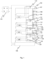
- Fig. 1 illustrates a circuit diagram of a LED lighting device according to an embodiment of the invention.
- the LED lighting device is AC-driven, and it comprises a full-wave rectifying circuit 101 that rectifies an AC voltage applied to its input terminals and outputs the rectified AC voltage at its output terminals to four LED circuits 102, 103, 104 and 105 that are connected in series.
- the current that is supplied to the LED circuits 102, 103, 104 and 105 is regulated with a current regulating circuit 106.
- the LED circuit 102 comprises a series connection of a flicker reduction circuit 107 and eight LEDs 108, and a capacitor 109 that is connected in parallel with this series connection.
- the LED circuit 102 also comprises a blocking diode 110.
- the anode of the blocking diode 110 is connected to a switching circuit 111 and the positive terminal of the rectifying circuit 101.
- the cathode of the blocking diode 110 is connected to the switching circuit 111, the flicker reduction circuit 107 and the positive terminal of the capacitor 109.
- the switching circuit 111 controls the flow of current through the LED circuit 102.
- the LED circuit 103 comprises a series connection of a flicker reduction circuit 112 and four LEDs 113, and a capacitor 114 that is connected in parallel with this series connection.
- the LED circuit 103 also comprises a blocking diode 115.
- the anode of the blocking diode 115 is connected to a switching circuit 116 and the LED circuit 102.
- the cathode of the blocking diode 115 is connected to the switching circuit 116, the flicker reduction circuit 112 and the positive terminal of the capacitor 114.
- the switching circuit 116 controls the flow of current through the LED circuit 103.
- the LED circuit 104 comprises a series connection of a flicker reduction circuit 117 and two LEDs 118, and a capacitor 119 that is connected in parallel with this series connection.
- the LED circuit 104 also comprises a blocking diode 120.
- the anode of the blocking diode 120 is connected to a switching circuit 121 and the LED circuit 103.
- the cathode of the blocking diode 120 is connected to the switching circuit 121, the flicker reduction circuit 117 and the positive terminal of the capacitor 119.
- the switching circuit 121 controls the flow of current through the LED circuit 104.
- the LED circuit 105 comprises a series connection of a flicker reduction circuit 122 and a LED 123, and a capacitor 124 that is connected in parallel with this series connection.
- the LED circuit 105 also comprises a blocking diode 125.
- the anode of the blocking diode 125 is connected to a switching circuit 126 and the LED circuit 104.
- the cathode of the blocking diode 125 is connected to the switching circuit 126, the flicker reduction circuit 122 and the positive terminal of the capacitor 124.
- the switching circuit 126 controls the flow of current through the LED circuit 105.
- the switching circuits 111, 116, 121 and 126 switch the LED circuits 102, 103, 104 and 105 on and off according to the voltage values at the positive terminals of the capacitors 109, 114, 119 and 124.
- Each switching circuit 111, 116, 121, 126 has specific first and second switching threshold voltages to allow for proper LED circuit control. The voltage at the positive terminal of the capacitor 109, 114, 119, 124 is compared to these threshold voltages.
- the first switching threshold voltage determines when the switching circuit 111, 116, 121, 126 turns off and allows current to charge the capacitor 109, 114, 119, 124 and to flow through the LED(s) 108, 113, 118, 123.
- the first switching threshold voltage is larger than the sum of the threshold voltages of the LED(s) 108, 113, 118, 123 in the corresponding LED circuit 102, 103, 104, 105.
- the second switching threshold voltage determines when the switching circuit 111, 116, 121, 126 turns on to shunt the LED(s) 108, 113, 118, 123 and allow the capacitor 109, 114, 119, 124 to discharge through the LED(s) 108, 113, 118, 123.
- the blocking diode 110, 115, 120, 125 prevents the capacitor 109, 114, 119, 124 from discharging through the switching circuit 111, 116, 121, 126.
- Fig. 2 illustrates a LED circuit in a LED lighting device according to an embodiment of the invention.
- the LED circuit 201 comprises a series connection of a flicker reduction circuit 202 and a plurality of LEDs 203.
- the flicker reduction circuit 202 comprises a current regulating element 204, a diode 205, a capacitor 206 and three resistors 207, 208 and 209.
- An anode of the diode 205 and an input terminal of the current regulating element 204 are connected to a first terminal 210 of the flicker reduction circuit 202.
- a cathode of the diode 205 is connected to a positive terminal of the capacitor 206 and a first terminal of the resistor 207.
- a control terminal of the current regulating element 204 is connected to a second terminal of the resistor 207 and a first terminal of the resistor 208.
- An output terminal of the current regulating element 204 is connected to a first terminal of the resistor 209.
- a negative terminal of the capacitor 206 and second terminals of the resistors 208 and 209 are connected to a second terminal 211 of the flicker reduction circuit 202.
- the LED circuit 201 comprises a capacitor 212 that is connected in parallel with the series connection of the flicker reduction circuit 202 and the plurality of LEDs 203, and a blocking diode 213 that is connected in series with this parallel connection.
- a switch 214 is used to control the flow of current through the LED circuit 201.
- the operation of the LED circuit 201 is illustrated by current and voltage waveforms shown in figs. 3A-3B .
- the first graph (A1) in fig. 3A presents the current that is supplied to the LED circuit 201.
- the waveform is the result of opening and closing the switch 214.
- the switch 214 When the switch 214 is open, the current is supplied to the LED circuit 201, whereby the capacitor 212 charges and the current flows through the LEDs 203.
- the switch 214 is closed, the capacitor 212 discharges through the LEDs 203.
- the blocking diode 213 prevents the capacitor 212 from discharging through the switch 214.
- the second graph (A2) in fig. 3A presents the current that flows through the LEDs 203.
- the third graph (V1) in fig. 3A presents the voltage across the flicker reduction circuit 202.
- the fourth graph (V2) in fig. 3A presents the voltage across the capacitor 206.
- Fig. 3B shows the voltage (V3) across the capacitor 212 and the voltage (V4) across the series-connected LEDs 203.
- V3 the voltage across the capacitor 212
- V4 the voltage across the series-connected LEDs 203.
- the voltage of the capacitor 212 contains a substantial ripple component.
- the voltage of the LEDs 203 does not contain ripple. As a result, the flicker produced by the LEDs 203 is minimal.
- Figs. 4A-4E illustrate flicker reduction circuits according to embodiments of the invention.
- the flicker reduction circuit of fig. 4A comprises an N-channel FET 401, a diode 402, a capacitor 403 and three resistors 404, 405 and 406.
- An anode of the diode 402 and a drain of the N-channel FET 401 are connected to a first terminal 407 of the circuit.
- a cathode of the diode 402 is connected to a positive terminal of the capacitor 403 and a first terminal of the resistor 404.
- a gate of the N-channel FET 401 is connected to a second terminal of the resistor 404 and a first terminal of the resistor 405.
- a source of the N-channel FET 401 is connected to a first terminal of the resistor 406.
- a negative terminal of the capacitor 403 and second terminals of the resistors 405 and 406 are connected to a second terminal 408 of the circuit.
- the flicker reduction circuit of fig. 4B differs from the one shown in fig. 4A in that the N-channel FET has been replaced with a Darlington pair using two NPN BJTs 409.
- the flicker reduction circuit of fig. 4C comprises a P-channel FET 410, a diode 402, a capacitor 403 and three resistors 404, 405 and 406.
- a positive terminal of the capacitor 403 and first terminals of the resistors 405 and 406 are connected to a first terminal 407 of the circuit.
- a negative terminal of the capacitor 403 is connected to an anode of the diode 402 and a first terminal of the resistor 404.
- a drain of the P-channel FET 410 is connected to a second terminal of the resistor 406, and a gate of the P-channel FET 410 is connected to second term inals of the resistors 404 and 405.
- a source of the P-channel FET 410 and a cathode of the diode 402 are connected to a second terminal 408 of the circuit.
- the flicker reduction circuit of fig. 4D differs from the one shown in fig. 4C in that the P-channel FET has been replaced with a Darlington pair using two PNP BJTs 411.
- the flicker reduction circuit of fig. 4E differs from the one shown in fig. 4A in that a resistor 412 has been connected between the drain and the source of the N-channel FET 401.
Landscapes
- Circuit Arrangement For Electric Light Sources In General (AREA)
Claims (12)
- Flimmerreduzierungsschaltung (107, 112, 117, 122, 202), umfassend:- ein Stromregelelement (204, 401, 409), das dazu konfiguriert ist, einen Strom zu regeln, der einer Reihenschaltung von mindestens einer LED (108, 113, 118, 123, 203) zugeführt wird, wobei das Stromregelelement (204, 401, 409) einen Eingangsanschluss, einen Ausgangsanschluss und einen Steueranschluss aufweist,- eine Diode (205, 402) und ein Kondensator (206, 403), die in Reihe geschaltet sind, wobei eine Anode der Diode (205, 402) mit einem ersten Anschluss (210, 407) der Flimmerreduzierungsschaltung (107, 112, 117, 122, 202) verbunden ist und ein negativer Anschluss des Kondensators (206, 403) mit einem zweiten Anschluss (211, 408) der Flimmerreduzierungsschaltung (107, 112, 117, 122, 202) verbunden ist,- einen ersten Widerstand (207, 404), der zwischen einem positiven Anschluss des Kondensators (206, 403) und dem Steueranschluss des Stromregelelements (204, 401, 409) angeschlossen ist, und- einen zweiten Widerstand (208, 405), der zwischen dem Steueranschluss des Stromregelelements (204, 401, 409) und dem zweiten Anschluss (211, 408) der Flimmerreduzierungsschaltung (107, 112, 117, 122, 202) angeschlossen ist,dadurch gekennzeichnet, dass der Eingangsanschluss des Stromregelelements (204, 401, 409) direkt mit dem ersten Anschluss (210, 407) der Flimmerreduzierungsschaltung (107, 112, 117, 122, 202) verbunden ist, und dass die Flimmerreduzierungsschaltung (107, 112, 117, 122, 202) ferner einen dritten Widerstand (209, 406) umfasst, der zwischen dem Ausgangsanschluss des Stromregelelements (204, 401, 409) und dem zweiten Anschluss (211, 408) der Flimmerreduzierungsschaltung (107, 112, 117, 122, 202) angeschlossen ist.
- . Flimmerreduzierungsschaltung (107, 112, 117, 122), umfassend:- ein Stromregelelement (410, 411), das dazu konfiguriert ist, einen Strom zu regeln, der einer Reihenschaltung von mindestens einer LED (108, 113, 118, 123) zugeführt wird, wobei das Stromregelelement (410, 411) einen Eingangsanschluss, einen Ausgangsanschluss und einen Steueranschluss aufweist,- einen Kondensator (403) und eine Diode (402), die in Reihe geschaltet sind,- einen ersten Widerstand (404), der zwischen einem Minuspol des Kondensators (403) und dem Steueranschluss des Stromregelelements (410, 411) geschaltet ist, und- einen zweiten Widerstand (405), der zwischen einem ersten Anschluss (407) der Flimmerreduzierungsschaltung (107, 112, 117, 122) und dem Steueranschluss des Stromregelelements (410, 411) geschaltet ist,dadurch gekennzeichnet, dass der Ausgangsanschluss des Stromregelelements (410, 411) direkt mit einem zweiten Anschluss (408) der Flimmerreduzierungsschaltung (107, 112, 117, 122) verbunden ist, ein positiver Anschluss des Kondensators (403) direkt mit dem ersten Anschluss (407) der Flimmerreduzierungsschaltung (107, 112, 117, 122) verbunden ist und eine Kathode der Diode (402) direkt mit dem zweiten Anschluss (408) der Flimmerreduzierungsschaltung (107, 112, 117, 122) verbunden ist, und dass die Flimmerreduzierungsschaltung (107, 112, 117, 122) ferner einen dritten Widerstand (406) umfasst, der zwischen dem ersten Anschluss (407) der Flimmerreduzierungsschaltung (107, 112, 117, 122) und dem Eingangsanschluss des Stromregelelements (410, 411) verbunden ist.
- . Flimmerreduzierungsschaltung (107, 112, 117, 122, 202) gemäß Anspruch 1 oder 2, wobei das Stromregelelement (204, 401, 409, 410, 411) eine oder mehrere der folgenden Komponenten umfasst: einen bipolaren Sperrschichttransistor, einen Feldeffekttransistor, einen bipolaren Isolierschichttransistor oder eine einstellbare Spannungsreferenz.
- . Flimmerreduzierungsschaltung (107, 112, 117, 122, 202) gemäß einem der vorhergehenden Ansprüche, wobei die Kapazität des Kondensators (206, 403) 1 bis 10 µF beträgt.
- . Flimmerreduzierungsschaltung (107, 112, 117, 122, 202) gemäß einem der vorhergehenden Ansprüche, wobei der Widerstandswert des ersten Widerstands (207, 404) 10 bis 1000 kΩ beträgt.
- . Flimmerreduzierungsschaltung (107, 112, 117, 122, 202) gemäß einem der vorhergehenden Ansprüche, wobei der Widerstandswert des zweiten Widerstands (208, 405) 10 bis 1000 kΩ beträgt.
- . Flimmerreduzierungsschaltung (107, 112, 117, 122, 202) gemäß einem der vorhergehenden Ansprüche, wobei der Widerstandswert des dritten Widerstands (209, 406) 1 bis 500 Ω beträgt.
- . Flimmerreduzierungsschaltung (107, 112, 117, 122, 202) gemäß einem der vorhergehenden Ansprüche, wobei die Flimmerreduzierungsschaltung (107, 112, 117, 122, 202) ferner einen vierten Widerstand (412) umfasst, der zwischen dem Eingangsanschluss und dem Ausgangsanschluss des Stromregelelements (401) angeschlossen ist.
- . Flimmerreduzierungsschaltung (107, 112, 117, 122, 202) gemäß Anspruch 8, wobei der Widerstandswert des vierten Widerstands (412) 100-5000 Ω beträgt.
- . LED-Beleuchtungsvorrichtung, umfassend:- eine Gleichrichterschaltung (101), die dazu konfiguriert ist, eine Wechselstrom-Eingangsspannung gleichzurichten,- eine Vielzahl von LED-Schaltungen (102, 103, 104, 105), wobei jede LED-Schaltung (102, 103, 104, 105) eine Reihenschaltung von mindestens einer LED (108, 113, 118, 123), einen parallel zu der Reihenschaltung geschalteten Kondensator (109, 114, 119, 124) und eine in Reihe zu der Parallelschaltung geschaltete Sperrdiode (110, 115, 120, 125) umfasst, wobei die Vielzahl von LED-Schaltungen (102, 103, 104, 105) eine ungleiche Anzahl von in Reihe geschalteten LEDs (108, 113, 118, 123) aufweist und in einer Reihenfolge in Reihe geschaltet ist, die durch die Anzahl der in Reihe geschalteten LEDs (108, 113, 118, 123) in jeder LED-Schaltung (102, 103, 104, 105) bestimmt wird, wobei die LED-Schaltung (102) mit der höchsten Anzahl in Reihe geschalteter LEDs (108) an einen Pluspol der Gleichrichterschaltung (101) angeschlossen ist, und- einen Schaltkreis (111, 116, 121, 126) für jede LED-Schaltung (102, 103, 104, 105), wobei die Schaltkreise (111, 116, 121, 126) so konfiguriert sind, dass sie den Stromfluss zur entsprechenden LED-Schaltung (102, 103, 104, 105) steuern,wobei mindestens einer der Vielzahl von LED-Schaltkreisen (102, 103, 104, 105) einen Flimmerreduzierungsschaltkreis (107, 112, 117, 122, 202) gemäß einem der vorhergehenden Ansprüche umfasst, der in Reihe mit den in Reihe geschalteten LEDs (108, 113, 118, 123) geschaltet ist.
- . LED-Beleuchtungsvorrichtung nach Anspruch 10, wobei die LED-Schaltung (102) mit der höchsten Anzahl an LEDs (108) mit der Flimmerreduzierungsschaltung (107) versehen ist.
- . LED-Beleuchtungsvorrichtung nach Anspruch 10 oder 11, wobei die LED-Beleuchtungsvorrichtung eine Stromregelschaltung (106) umfasst, die dazu konfiguriert ist, einen der Vielzahl von LED-Schaltungen (102, 103, 104, 105) zugeführten Strom zu regeln.
Priority Applications (1)
| Application Number | Priority Date | Filing Date | Title |
|---|---|---|---|
| EP21167384.3A EP4072248B1 (de) | 2021-04-08 | 2021-04-08 | Flimmerreduktionsschaltung |
Applications Claiming Priority (1)
| Application Number | Priority Date | Filing Date | Title |
|---|---|---|---|
| EP21167384.3A EP4072248B1 (de) | 2021-04-08 | 2021-04-08 | Flimmerreduktionsschaltung |
Publications (3)
| Publication Number | Publication Date |
|---|---|
| EP4072248A1 EP4072248A1 (de) | 2022-10-12 |
| EP4072248C0 EP4072248C0 (de) | 2024-08-07 |
| EP4072248B1 true EP4072248B1 (de) | 2024-08-07 |
Family
ID=75438618
Family Applications (1)
| Application Number | Title | Priority Date | Filing Date |
|---|---|---|---|
| EP21167384.3A Active EP4072248B1 (de) | 2021-04-08 | 2021-04-08 | Flimmerreduktionsschaltung |
Country Status (1)
| Country | Link |
|---|---|
| EP (1) | EP4072248B1 (de) |
Family Cites Families (3)
| Publication number | Priority date | Publication date | Assignee | Title |
|---|---|---|---|---|
| KR101673852B1 (ko) * | 2014-05-07 | 2016-11-22 | 주식회사 실리콘웍스 | 발광 다이오드 조명 장치의 제어 회로 |
| IT201700032546A1 (it) * | 2017-03-24 | 2018-09-24 | Cynergi S R L | Circuito elettronico per il pilotaggio di una stringa di diodi ad emissione di luce |
| KR102018365B1 (ko) * | 2017-10-26 | 2019-09-04 | 공명국 | 플리커 방지용 led 조명 장치 |
-
2021
- 2021-04-08 EP EP21167384.3A patent/EP4072248B1/de active Active
Also Published As
| Publication number | Publication date |
|---|---|
| EP4072248C0 (de) | 2024-08-07 |
| EP4072248A1 (de) | 2022-10-12 |
Similar Documents
| Publication | Publication Date | Title |
|---|---|---|
| CN103974502B (zh) | Led光引擎的电子控制装置及其应用 | |
| US9095021B2 (en) | Circuit arrangement for operating at least a first and a second cascade of LEDs | |
| US20120068616A1 (en) | Led drive circuit | |
| WO2012168828A2 (en) | Led light source | |
| KR20130117651A (ko) | 적응형 회로 | |
| CN107801271A (zh) | 点亮装置和车辆 | |
| US9713207B2 (en) | Driver module for driving LEDs | |
| US20190037659A1 (en) | Led driver and led lamp using the same | |
| US10201048B2 (en) | Lighting apparatus | |
| US20150327341A1 (en) | Control circuit of led lighting apparatus | |
| KR101357636B1 (ko) | 플리커 제거 기능의 고효율 직결형 엘이디 구동 회로 | |
| US9730287B2 (en) | Lighting apparatus and dimming regulation circuit thereof | |
| CN104797037A (zh) | 具备多级驱动阶段和低频闪的发光二极管照明装置 | |
| US9532412B2 (en) | Lighting apparatus capable of reducing flicker | |
| KR20200130061A (ko) | Led 구동 캐패시터를 포함하는 ac 직결형 발광 다이오드 구동장치 | |
| JP2020198752A (ja) | 電源装置、半導体集積回路及びリップル抑制方法 | |
| EP4072248A1 (de) | Flimmerreduktionsschaltung | |
| US20180328551A1 (en) | Led lighting apparatus | |
| US11224103B2 (en) | LED lighting apparatus | |
| KR101279493B1 (ko) | 전원공급회로 | |
| US10076008B2 (en) | Optoelectronic circuit comprising light-emitting diodes | |
| US10912169B2 (en) | LED lighting apparatus | |
| US9930735B1 (en) | Low-flicker light-emitting diode lighting device | |
| US20180368226A1 (en) | Led lighting apparatus | |
| US20230094863A1 (en) | A power converter having multiple main switches in series and a power conversion method |
Legal Events
| Date | Code | Title | Description |
|---|---|---|---|
| PUAI | Public reference made under article 153(3) epc to a published international application that has entered the european phase |
Free format text: ORIGINAL CODE: 0009012 |
|
| STAA | Information on the status of an ep patent application or granted ep patent |
Free format text: STATUS: THE APPLICATION HAS BEEN PUBLISHED |
|
| AK | Designated contracting states |
Kind code of ref document: A1 Designated state(s): AL AT BE BG CH CY CZ DE DK EE ES FI FR GB GR HR HU IE IS IT LI LT LU LV MC MK MT NL NO PL PT RO RS SE SI SK SM TR |
|
| RAP1 | Party data changed (applicant data changed or rights of an application transferred) |
Owner name: CONTROLLED OY |
|
| STAA | Information on the status of an ep patent application or granted ep patent |
Free format text: STATUS: REQUEST FOR EXAMINATION WAS MADE |
|
| 17P | Request for examination filed |
Effective date: 20230406 |
|
| RBV | Designated contracting states (corrected) |
Designated state(s): AL AT BE BG CH CY CZ DE DK EE ES FI FR GB GR HR HU IE IS IT LI LT LU LV MC MK MT NL NO PL PT RO RS SE SI SK SM TR |
|
| GRAP | Despatch of communication of intention to grant a patent |
Free format text: ORIGINAL CODE: EPIDOSNIGR1 |
|
| STAA | Information on the status of an ep patent application or granted ep patent |
Free format text: STATUS: GRANT OF PATENT IS INTENDED |
|
| RIC1 | Information provided on ipc code assigned before grant |
Ipc: H05B 45/48 20200101ALI20240327BHEP Ipc: H05B 45/395 20200101ALI20240327BHEP Ipc: H05B 45/345 20200101AFI20240327BHEP |
|
| INTG | Intention to grant announced |
Effective date: 20240417 |
|
| GRAS | Grant fee paid |
Free format text: ORIGINAL CODE: EPIDOSNIGR3 |
|
| GRAA | (expected) grant |
Free format text: ORIGINAL CODE: 0009210 |
|
| STAA | Information on the status of an ep patent application or granted ep patent |
Free format text: STATUS: THE PATENT HAS BEEN GRANTED |
|
| AK | Designated contracting states |
Kind code of ref document: B1 Designated state(s): AL AT BE BG CH CY CZ DE DK EE ES FI FR GB GR HR HU IE IS IT LI LT LU LV MC MK MT NL NO PL PT RO RS SE SI SK SM TR |
|
| REG | Reference to a national code |
Ref country code: GB Ref legal event code: FG4D |
|
| REG | Reference to a national code |
Ref country code: CH Ref legal event code: EP |
|
| REG | Reference to a national code |
Ref country code: IE Ref legal event code: FG4D |
|
| REG | Reference to a national code |
Ref country code: DE Ref legal event code: R096 Ref document number: 602021016669 Country of ref document: DE |
|
| U01 | Request for unitary effect filed |
Effective date: 20240819 |
|
| U07 | Unitary effect registered |
Designated state(s): AT BE BG DE DK EE FI FR IT LT LU LV MT NL PT RO SE SI Effective date: 20240909 |
|
| PG25 | Lapsed in a contracting state [announced via postgrant information from national office to epo] |
Ref country code: NO Free format text: LAPSE BECAUSE OF FAILURE TO SUBMIT A TRANSLATION OF THE DESCRIPTION OR TO PAY THE FEE WITHIN THE PRESCRIBED TIME-LIMIT Effective date: 20241107 |
|
| PG25 | Lapsed in a contracting state [announced via postgrant information from national office to epo] |
Ref country code: PL Free format text: LAPSE BECAUSE OF FAILURE TO SUBMIT A TRANSLATION OF THE DESCRIPTION OR TO PAY THE FEE WITHIN THE PRESCRIBED TIME-LIMIT Effective date: 20240807 Ref country code: GR Free format text: LAPSE BECAUSE OF FAILURE TO SUBMIT A TRANSLATION OF THE DESCRIPTION OR TO PAY THE FEE WITHIN THE PRESCRIBED TIME-LIMIT Effective date: 20241108 |
|
| PG25 | Lapsed in a contracting state [announced via postgrant information from national office to epo] |
Ref country code: IS Free format text: LAPSE BECAUSE OF FAILURE TO SUBMIT A TRANSLATION OF THE DESCRIPTION OR TO PAY THE FEE WITHIN THE PRESCRIBED TIME-LIMIT Effective date: 20241207 |
|
| PG25 | Lapsed in a contracting state [announced via postgrant information from national office to epo] |
Ref country code: HR Free format text: LAPSE BECAUSE OF FAILURE TO SUBMIT A TRANSLATION OF THE DESCRIPTION OR TO PAY THE FEE WITHIN THE PRESCRIBED TIME-LIMIT Effective date: 20240807 |
|
| PG25 | Lapsed in a contracting state [announced via postgrant information from national office to epo] |
Ref country code: ES Free format text: LAPSE BECAUSE OF FAILURE TO SUBMIT A TRANSLATION OF THE DESCRIPTION OR TO PAY THE FEE WITHIN THE PRESCRIBED TIME-LIMIT Effective date: 20240807 Ref country code: RS Free format text: LAPSE BECAUSE OF FAILURE TO SUBMIT A TRANSLATION OF THE DESCRIPTION OR TO PAY THE FEE WITHIN THE PRESCRIBED TIME-LIMIT Effective date: 20241107 |
|
| PG25 | Lapsed in a contracting state [announced via postgrant information from national office to epo] |
Ref country code: RS Free format text: LAPSE BECAUSE OF FAILURE TO SUBMIT A TRANSLATION OF THE DESCRIPTION OR TO PAY THE FEE WITHIN THE PRESCRIBED TIME-LIMIT Effective date: 20241107 Ref country code: PL Free format text: LAPSE BECAUSE OF FAILURE TO SUBMIT A TRANSLATION OF THE DESCRIPTION OR TO PAY THE FEE WITHIN THE PRESCRIBED TIME-LIMIT Effective date: 20240807 Ref country code: NO Free format text: LAPSE BECAUSE OF FAILURE TO SUBMIT A TRANSLATION OF THE DESCRIPTION OR TO PAY THE FEE WITHIN THE PRESCRIBED TIME-LIMIT Effective date: 20241107 Ref country code: IS Free format text: LAPSE BECAUSE OF FAILURE TO SUBMIT A TRANSLATION OF THE DESCRIPTION OR TO PAY THE FEE WITHIN THE PRESCRIBED TIME-LIMIT Effective date: 20241207 Ref country code: HR Free format text: LAPSE BECAUSE OF FAILURE TO SUBMIT A TRANSLATION OF THE DESCRIPTION OR TO PAY THE FEE WITHIN THE PRESCRIBED TIME-LIMIT Effective date: 20240807 Ref country code: GR Free format text: LAPSE BECAUSE OF FAILURE TO SUBMIT A TRANSLATION OF THE DESCRIPTION OR TO PAY THE FEE WITHIN THE PRESCRIBED TIME-LIMIT Effective date: 20241108 Ref country code: ES Free format text: LAPSE BECAUSE OF FAILURE TO SUBMIT A TRANSLATION OF THE DESCRIPTION OR TO PAY THE FEE WITHIN THE PRESCRIBED TIME-LIMIT Effective date: 20240807 |
|
| PG25 | Lapsed in a contracting state [announced via postgrant information from national office to epo] |
Ref country code: SM Free format text: LAPSE BECAUSE OF FAILURE TO SUBMIT A TRANSLATION OF THE DESCRIPTION OR TO PAY THE FEE WITHIN THE PRESCRIBED TIME-LIMIT Effective date: 20240807 |
|
| PG25 | Lapsed in a contracting state [announced via postgrant information from national office to epo] |
Ref country code: CZ Free format text: LAPSE BECAUSE OF FAILURE TO SUBMIT A TRANSLATION OF THE DESCRIPTION OR TO PAY THE FEE WITHIN THE PRESCRIBED TIME-LIMIT Effective date: 20240807 |
|
| PG25 | Lapsed in a contracting state [announced via postgrant information from national office to epo] |
Ref country code: SK Free format text: LAPSE BECAUSE OF FAILURE TO SUBMIT A TRANSLATION OF THE DESCRIPTION OR TO PAY THE FEE WITHIN THE PRESCRIBED TIME-LIMIT Effective date: 20240807 |
|
| U20 | Renewal fee for the european patent with unitary effect paid |
Year of fee payment: 5 Effective date: 20250415 |
|
| PLBE | No opposition filed within time limit |
Free format text: ORIGINAL CODE: 0009261 |
|
| STAA | Information on the status of an ep patent application or granted ep patent |
Free format text: STATUS: NO OPPOSITION FILED WITHIN TIME LIMIT |
|
| 26N | No opposition filed |
Effective date: 20250508 |
|
| REG | Reference to a national code |
Ref country code: CH Ref legal event code: H13 Free format text: ST27 STATUS EVENT CODE: U-0-0-H10-H13 (AS PROVIDED BY THE NATIONAL OFFICE) Effective date: 20251125 |
|
| PG25 | Lapsed in a contracting state [announced via postgrant information from national office to epo] |
Ref country code: MC Free format text: LAPSE BECAUSE OF FAILURE TO SUBMIT A TRANSLATION OF THE DESCRIPTION OR TO PAY THE FEE WITHIN THE PRESCRIBED TIME-LIMIT Effective date: 20240807 |
|
| GBPC | Gb: european patent ceased through non-payment of renewal fee |
Effective date: 20250408 |
|
| PG25 | Lapsed in a contracting state [announced via postgrant information from national office to epo] |
Ref country code: GB Free format text: LAPSE BECAUSE OF NON-PAYMENT OF DUE FEES Effective date: 20250408 |
|
| PG25 | Lapsed in a contracting state [announced via postgrant information from national office to epo] |
Ref country code: CH Free format text: LAPSE BECAUSE OF NON-PAYMENT OF DUE FEES Effective date: 20250430 |
|
| PG25 | Lapsed in a contracting state [announced via postgrant information from national office to epo] |
Ref country code: IE Free format text: LAPSE BECAUSE OF NON-PAYMENT OF DUE FEES Effective date: 20250408 |
|
| U20 | Renewal fee for the european patent with unitary effect paid |
Year of fee payment: 6 Effective date: 20260417 |
|
| PG25 | Lapsed in a contracting state [announced via postgrant information from national office to epo] |
Ref country code: CY Free format text: LAPSE BECAUSE OF FAILURE TO SUBMIT A TRANSLATION OF THE DESCRIPTION OR TO PAY THE FEE WITHIN THE PRESCRIBED TIME-LIMIT Effective date: 20240807 |