EP4072246B1 - Dispositif de fonctionnement pour moyens d'éclairage - Google Patents
Dispositif de fonctionnement pour moyens d'éclairage Download PDFInfo
- Publication number
- EP4072246B1 EP4072246B1 EP21166894.2A EP21166894A EP4072246B1 EP 4072246 B1 EP4072246 B1 EP 4072246B1 EP 21166894 A EP21166894 A EP 21166894A EP 4072246 B1 EP4072246 B1 EP 4072246B1
- Authority
- EP
- European Patent Office
- Prior art keywords
- voltage
- operating device
- circuitry
- signal
- lighting means
- Prior art date
- Legal status (The legal status is an assumption and is not a legal conclusion. Google has not performed a legal analysis and makes no representation as to the accuracy of the status listed.)
- Active
Links
Images


Classifications
-
- H—ELECTRICITY
- H05—ELECTRIC TECHNIQUES NOT OTHERWISE PROVIDED FOR
- H05B—ELECTRIC HEATING; ELECTRIC LIGHT SOURCES NOT OTHERWISE PROVIDED FOR; CIRCUIT ARRANGEMENTS FOR ELECTRIC LIGHT SOURCES, IN GENERAL
- H05B45/00—Circuit arrangements for operating light-emitting diodes [LED]
- H05B45/10—Controlling the intensity of the light
-
- H—ELECTRICITY
- H05—ELECTRIC TECHNIQUES NOT OTHERWISE PROVIDED FOR
- H05B—ELECTRIC HEATING; ELECTRIC LIGHT SOURCES NOT OTHERWISE PROVIDED FOR; CIRCUIT ARRANGEMENTS FOR ELECTRIC LIGHT SOURCES, IN GENERAL
- H05B45/00—Circuit arrangements for operating light-emitting diodes [LED]
- H05B45/30—Driver circuits
- H05B45/32—Pulse-control circuits
- H05B45/325—Pulse-width modulation [PWM]
-
- H—ELECTRICITY
- H05—ELECTRIC TECHNIQUES NOT OTHERWISE PROVIDED FOR
- H05B—ELECTRIC HEATING; ELECTRIC LIGHT SOURCES NOT OTHERWISE PROVIDED FOR; CIRCUIT ARRANGEMENTS FOR ELECTRIC LIGHT SOURCES, IN GENERAL
- H05B45/00—Circuit arrangements for operating light-emitting diodes [LED]
- H05B45/30—Driver circuits
- H05B45/37—Converter circuits
-
- H—ELECTRICITY
- H05—ELECTRIC TECHNIQUES NOT OTHERWISE PROVIDED FOR
- H05B—ELECTRIC HEATING; ELECTRIC LIGHT SOURCES NOT OTHERWISE PROVIDED FOR; CIRCUIT ARRANGEMENTS FOR ELECTRIC LIGHT SOURCES, IN GENERAL
- H05B45/00—Circuit arrangements for operating light-emitting diodes [LED]
- H05B45/50—Circuit arrangements for operating light-emitting diodes [LED] responsive to malfunctions or undesirable behaviour of LEDs; responsive to LED life; Protective circuits
Definitions
- the invention is, generally, in the area of operating devices for lighting means, which are controllable by means of NFC communication.
- NFC Near Field Communication
- modules can be used for configuring LED drivers or other operating devices for lighting means.
- a control circuitry of the LED driver or operating device such as a microcontroller, can be used in order to communicate with the NFC module.
- NFC modules to translate a configuration signal for the LED driver into a pulse-width-modulated signal (e.g., representing an LED current) which can be fed to an integrated control circuit of the LED-driver without the need of further intelligence, such as an extra control circuitry or microcontroller.
- a pulse-width-modulated signal e.g., representing an LED current
- such NFC modules convert a NFC signal into a PWM signal via an integrated circuitry on the NFC module, wherein the duty cycle of the PWM signal reflects the wirelessly received signal.
- a control circuitry for operating devices for lighting means can comprise a programming input pin, at which such analog DC voltage may be supplied in order to input a nominal value for the current through the lighting means, especially through an LED load.
- the nominal current for LEDs may be programmed.
- US 2020/0313727 A1 discloses a power regulation for lighting using NFC.
- a NFC transceiver is used to make the programming of the nominal set-point easier.
- DC level feature which allows to detect and distinguish between an AC and a DC supply voltage. It is, however, difficult to implement such a DC level feature in an operating device without making use of additional intelligence.
- the invention relates to an operating device for lighting means, comprising: output terminals supplying lighting means, such as e.g. a LED load, a control circuitry for controlling the electrical supply of the lighting means, a NFC module configured to receive NFC signals and output a pulse width modulation, PWM, signal with variable duty cycle, a conversion circuitry arranged for being supplied with the PWM signal and for outputting a DC voltage supplied to an input of the control circuitry.
- the DC voltage is a function of the duty cycle of the PWM signal according to a set conversion rate and the conversion circuitry is configured to be supplied with an internal control signal to set at least two conversion rates.
- the control circuitry may be a microcontroller.
- the control signal may comprise an AC or DC voltage signal
- the operating device comprises a detection circuitry configured to detect if a supply voltage of the operating device is a AC or DC voltage and to set the control signal for the conversion rate differently in case of the presence of a AC or DC signal, respectively.
- control circuitry is configured to map the level of the supplied DC voltage into a nominal current for the LED load and to control the operation of the lighting means, e.g. by controlling a switch operation of at least one switch of a switched converter such that an actual current matches the nominal current.
- the conversion rate can be varied continuously or incrementally in steps by said control signal.
- the conversion circuitry comprises a R-C low pass filter configured to convert the PWM signal into the DC voltage.
- the operating device comprises a detection circuitry configured to detect if a supply voltage of the operating device is an AC or DC voltage and to set the control signal for the conversion rate differently in case of the presence of an AC or DC signal, respectively.
- the operating device has a DC level feature, i.e. it can detect whether a mains voltage is an AC or a DC voltage.
- a detection of a DC signal such as from a battery inside the operating device
- the output current of the operating device for lighting means e.g., LED driver
- the detection circuitry comprises a voltage divider or a R-C low pass filter or a capacitor.
- the operating device comprises a limiting circuitry configured to limit the DC voltage in case the set control signal is a DC signal.
- the limiting circuitry comprises a Zener diode configured to clamp the DC signal.
- the limiting circuitry comprises a switch configured to switch if the control signal is a DC signal.
- the switch is configured to switch on a connection between the detection circuitry and the limiting circuitry.
- the NFC module is configured to program a nominal current of the LED load.
- the invention relates to a system comprising a NFC transmitting handheld device and an operating device according to the first aspect or any one of the implementation forms thereof.
- the invention relates to a method for operating a device for lighting means, comprising: supplying lighting means, such as LED load, by output terminals; controlling the electrical supply of the lighting means; receiving NFC signals; outputting a pulse width modulation, PWM, signal with variable duty cycle; supplying a conversion circuitry with the PWM signal; outputting a DC voltage supplied to an input of a control circuitry, wherein the DC voltage is a function of the duty cycle of the PWM signal according to a set conversion rate, wherein the conversion circuitry is configured to be supplied with an internal control signal to set at least two conversion rates, wherein the operating device (400) comprises a detection circuitry (402) configured to detect if a supply voltage of the operating device is a AC or DC voltage and to set the control signal for the conversion rate differently in case of the presence of a AC or DC signal, respectively.
- the operating device comprises a detection circuitry (402) configured to detect if a supply voltage of the operating device is a AC or DC voltage and to set the control signal for the conversion rate
- LED luminaire shall mean a luminaire with a light source comprising one or more LEDs or OLEDs. LEDs are well-known in the art, and therefore, will only briefly be discussed to provide a complete description of the invention.
- the aspect of the present invention might contain integrated circuits that are readily manufacturable using conventional semiconductor technologies, such as complementary metal-oxide semiconductor technology, short "CMOS".
- CMOS complementary metal-oxide semiconductor technology
- the aspects of the present invention may be implemented with other manufacturing processes for making optical as well as electrical devices.
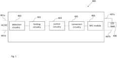
- Fig. 1 shows a schematic representation of an operating device 400 for lighting means 408 according to an embodiment.
- the operating device 400 for lighting means 408 can be fed with an AC or DC voltage at the input terminals 401a and 401b.
- the operating device 400 for lighting means 408 comprises: output terminals 407a, 407b supplying lighting means 408, such as e.g. a LED load, a control circuitry 404 for controlling an electrical supply of the lighting means 408; a NFC module 406 configured to receive NFC signals and output a pulse width modulation, PWM, signal with variable duty cycle; a conversion circuitry 405 arranged for being supplied with the PWM signal and for outputting a DC voltage supplied to an input of the control circuitry 404.
- the DC voltage is a function of the duty cycle of the PWM signal according to a set conversion rate, and the conversion circuitry 405 is configured to be supplied with an internal control signal to set at least two conversion rates.
- the internal control signal can comprise an AC or DC voltage signal.
- the operating device 400 can comprise a detection circuitry 402 configured to detect if a supply voltage of the operating device is a AC or DC voltage and to set the control signal for the conversion rate differently in case of the presence of a AC or DC signal, respectively.
- the operating device 400 can comprise a limiting circuitry 403 configured to limit the DC voltage in case the set control signal is a DC signal.
- the NFC module 406 can be configured to translate a current configuration into a pulse-width-modulation (PWM) signal which, then, can be filtered and used as current selection information for a LED control integration circuit or control circuitry 404.
- PWM pulse-width-modulation
- the output current of the LED driver or operating device 400 can be reduced, so that, for example, a battery inside the LED driver or operating device 400 can last longer, for example, in emergency situations.
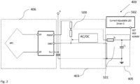
- Fig. 2 shows a schematic representation of the operating device 400 for lighting means 408 according to an embodiment.
- Fig. 2 shows a NFC module 406 (antenna and processing circuitry) connected to a voltage divider 500 which is connected to a low pass R-C filter 501.
- the R-C filter 501 forms the conversion circuitry 405.
- a dim voltage Vdim at the output of the R-C filter 501 can depend on the duty cycle of the PWM signal.
- the pulse-width-modulation (PWM) of the input signal of the NFC module 406 correlates linearly with the set LED current.
- the frequency of the PWM signal can be in the range of 1 kHz - 30 kHz, while the PWM voltage levels can be in the range of 0 V - 2,8 V.
- an analog signal can be obtained.
- an AC/DC signal is provided as input to the limiting circuitry 403 and the voltage divider 500 comprising two resistors is connected to the NFC module 406 and the R-C filter 501.
- the module 502 of the operating device 400 can comprise the control circuitry 404 (not shown in Fig. 2 ).
- the operating device 400 can be adapted to operate in different configurations: either a high level of the PWM signal at the output of the NFC module 406 can be adapted depending on the supply signal (configuration options 1a and 1b), or a filtered analog signal at the output of the R-C low-pass filter 501 can be adapted (configuration option 2a and 2b) depending on the supply signal.
- the supply signal may refer to the supply voltage of the operating device 400.
- the high level of the PWM signal at the output of the NFC module 406 is adapted via the voltage divider 500, which divides the voltage in case of a DC supply signal. In case of an AC supply signal, the voltage is not divided.
- Fig. 3 shows a schematic representation of the operating device 400 for lighting means 408 according to an embodiment.
- Fig. 3 shows a circuitry similar to the one shown in Fig. 2 .
- a Zener diode 600 is added to the circuitry, and an AC/DC voltage is given as input to the Zener diode 600.
- the high level of the PWM signal at the output of the NFC module 406 is adapted via the Zener diode 600.
- the voltage In case of a DC voltage, the voltage is clamped by the Zener diode 600, while in case of an AC voltage, the voltage is not clamped.
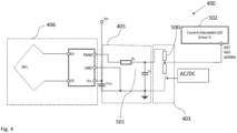
- Fig. 4 shows a schematic representation of the operating device 400 for lighting means 408 according to an embodiment.
- Fig. 4 shows a circuitry similar to the circuitry of Fig. 2 , wherein the voltage divider 500 is added at the output of the R-C low pass filter 501, instead of at the output of the NFC module 406.
- the analog signal at the output of the R-C filter is adapted by the voltage divider 500. In case of a DC input voltage, the voltage is divided, while in case of an AC voltage, the voltage is not divided.
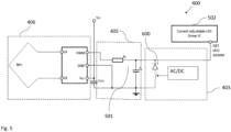
- Fig. 5 shows a schematic representation of the operating device 400 for lighting means 408 according to an embodiment.
- Fig. 5 shows a circuitry similar to the one of Fig. 2 , wherein a Zener diode 600 is added to the circuit at the output of the R-C low pass filter 501.
- the filtered analog signal at the output of the R-C low pass filter is adapted via the Zener diode 600.
- the voltage is clamped, while in case of AC input voltage, the voltage is not clamped.
- Fig. 6 shows a schematic representation of PWM signals and voltage signals in the operating device 400 for lighting means 408 according to an embodiment.
- Fig. 6 shows the effect of the DC level feature of the operating device 400 in case of an AC supply signal.
- the PWM NFC signal at the output of the NFC module 406 is shown in case of the configuration options 1a, 1b, 2a and 2b on the upper panel (case "PWM NFC chip out'').
- the PWM signal at the RC-filter input is shown on the middle panel for the configuration options 1a, 1b, 2a and 2b (case "PWM RC-filter in'').
- Vdim or DC voltage namely the voltage at the output of the R-C low-pass filter 501, is shown as a function of the duty-cycle of the PWM signal on the lower panel for the configuration options 1a, 1b, 2a and 2b (case "Vdim vs. duty-cycle'').
- the voltage Vdim or DC voltage does not change in any configuration option.
- the DC level or conversion rate can be set in the range of 0-100% dim level, while in other devices it can be fixed at, e.g., 70% of dim level.
- Fig. 7 shows a schematic representation of PWM signals and voltage signals in the operating device 400 for lighting means 408 according to an embodiment.
- Fig. 7 shows the effect of the DC level feature of the operating device 400 in case of a DC supply signal.
- the PWM NFC signal at the output of the NFC module 406 is shown for all configuration options 1a, 1b, 2a and 2b on the upper panel (case "PWM NFC chip out'').
- the PWM signal at the input of the RC-filter 501 is shown on the middle panel for the all configuration options 1a, 1b, 2a and 2b (case "PWM RC-filter in''). As it can be taken from Fig. 7 , in this case, the DC voltage level is lowered at the input of the PWM R-C filter 501 for the configuration options 1a and 1b.
- the dimmed voltage Vdim or DC voltage namely the voltage at the output of the R-C low-pass filter 501
- Vdim vs. duty-cycle the dimmed voltage or DC voltage as a function of the duty-cycle of the PWM signal reaches its highest value, namely the DC voltage level.
- the voltage Vdim is influenced by connecting a voltage divider 500 or a Zener diode 600 by a switch if, e.g., a DC mains voltage is applied. Therefore, a circuit can be implemented in order to switch in case of a DC mains, as it will be described with reference to the following figures.
- Fig. 8 shows a schematic representation of the operating device 400 for lighting means 408 according to an embodiment.
- the operating device 400 for lighting means 408 comprises the detection circuitry 402, the limiting circuitry 403 and a rectifying bridge 1105.
- the detection circuitry 402 comprises two rectifying diodes 1101, a voltage divider 1100, a R-C filter 1102 and a capacitor 1103.
- the input voltage comes from the L and N wires, wherein the input voltage is rectified by the rectifying bridge 1105.
- the limiting circuit 403 comprises a switch 1104.
- the time constant of the R-C filter is much longer than 10 ms and the switch 1104, e.g. FET, does not switch. This can also be seen in the plot of the threshold value th 1106 which is higher than the voltage value which allows for the switch 1104 to switch.
- Fig. 9 shows a schematic representation of the operating device 400 for lighting means 408 according to an embodiment.
- the capacitor 1103 is charged according to the time constant of R-C low-pass filter and the switch 1104 FET switches. This can also be seen in the plot of the threshold value th 1106 which is lower than the voltage value which allows for the switch 1104 to switch.
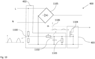
- Fig. 10 shows a schematic representation of the operating device 400 for lighting means 408 according to an embodiment.
- Fig. 10 shows a circuitry analogous to the one of Fig. 8 and Fig. 9 , besides that the detection circuitry 402 does not comprise the rectifying diodes 1101. Moreover, in this embodiment, only the L wire is sensed. This provides the advantage that sensing only L is cheaper.
- the time constant of the R-C low-pass filter 1102 is much longer than 20 ms, and the switch 1104 FET does not switch. This can also be seen in the plot of the threshold value th 1106 which is higher than the voltage value which allows for the switch 1104 to switch.
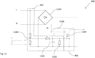
- Fig. 11 shows a schematic representation of the operating device 400 for lighting means 408 according to an embodiment.
- Fig. 11 shows a circuitry analogous to the one shown in Fig. 10 .
- the capacitor 1103 is charged according to the time constant of the R-C low-pass filter 1102 and the switch 1104 FET switches. This can also be seen in the plot of the threshold value th 1106 which is lower than the voltage value which allows for the switch 1104 to switch.
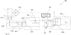
- Fig. 12 shows a schematic representation of the operating device 400 for lighting means 408 according to an embodiment.
- Fig. 12 shows a selection of some of the elements which can be comprised in the operating device 400 for lighting means 408 according to an embodiment.
- the operating device 400 in Fig. 12 comprises the detection circuitry 402, the limiting circuitry 403, the conversion circuitry 405, the NFC module 406 and a rectifying bridge 1105.
- the signal coming from the L and N wires is given as input to the detecting circuitry 402.
- the detecting circuitry 402 can comprise two rectifying diodes 1101, a voltage divider 1100, a R-C low pass filter 1102 and a capacitor 1103.
- the limiting circuity 403 can comprise a switch 1104 and a Zener diode 600.
- the switch 600 is configured to switch if the input signal or control signal is a DC signal.
- the NFC module 406 comprises an NFC antenna which transmits a signal to the unit 406a which, in turn, converts the received signal into a PWM signal.
- the PWM signal is given as input signal to the conversion circuitry 405.
- the conversion circuitry 405 comprises the R-C low-pass filter 501.
- the output signal of the R-C filter 501 is given as input to the module 502 which comprises the control circuitry 404 (not shown in Fig. 12 ).
- Fig. 12 shows an example of a limiting circuitry 403 for a DC level or conversion rate of 70%.
- the configuration option 2b of influencing the Vdim signal or DC voltage via the Zener 600 at the R-C low-pass filter 501 output and the configuration option 1a and 1b of detecting the DC voltage and switching via sensing L and N are used.
- the high level of the PWM signal output of the NFC module 406 is influenced in such a way, that the resulting analog signal at the output of the R-C low pass filter 501 is relating to a DC dim level relatively to the selected LED current or the current of the operating device 400 via the NFC module 406.
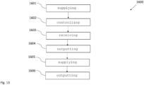
- Fig. 13 shows a schematic representation of a method 1600 for operating a device 400 for lighting means 408 according to an embodiment.
- the method 1600 comprises the steps of:
Landscapes
- Circuit Arrangement For Electric Light Sources In General (AREA)
Claims (11)
- Dispositif de fonctionnement pour des moyens d'éclairage (400), comprenant :- des bornes de sortie (407a, 407b) alimentant des moyens d'éclairage (408), tels que, par exemple, une charge DEL,- un ensemble de circuits de commande (404) pour commander une alimentation électrique des moyens d'éclairage (408) ;- un module CCP (406) configuré pour recevoir des signaux CCP et émettre un signal de modulation d'impulsions en largeur, PWM, à cycle de service variable ;- un ensemble de circuits de conversion (405) agencé pour être alimenté avec le signal PWM et pour émettre une tension continue alimentée à une entrée de l'ensemble de circuits de commande (404), caractérisé en ce que la tension continue alimentée est une fonction du cycle de service du signal PWM en fonction d'un taux de conversion défini,l'ensemble de circuits de conversion (405) est configuré pour être alimenté avec un signal de commande interne afin de définir au moins deux taux de conversion,dans lequel le dispositif de fonctionnement (400) comprend un ensemble de circuits de détection (402) configuré pour détecter si une tension d'alimentation du dispositif de fonctionnement est une tension alternative ou continue et pour définir le signal de commande interne pour le taux de conversion différemment en cas de présence d'une tension alternative ou continue, respectivement.
- Dispositif de fonctionnement (400) selon la revendication 1, dans lequel l'ensemble de circuits de commande (404) est configuré pour adapter le niveau de la tension continue alimentée en un courant nominal pour les moyens d'éclairage et pour commander le fonctionnement des moyens d'éclairage (408), par exemple en commandant le fonctionnement de commutateur d'au moins un commutateur d'un convertisseur commuté de sorte qu'un courant réel correspond au courant nominal.
- Dispositif de fonctionnement (400) selon la revendication 1 ou 2, dans lequel le taux de conversion peut être modifié de façon continue ou incrémentale par étapes par ledit signal de commande interne.
- Dispositif de fonctionnement (400) selon l'une quelconque des revendications précédentes, dans lequel l'ensemble de circuits de conversion (405) comprend un filtre passe-bas R-C (501) configuré pour convertir le signal PWM en tension continue alimentée.
- Dispositif de fonctionnement (400) selon l'une quelconque des revendications précédentes, dans lequel l'ensemble de circuits de commande (402) comprend un diviseur de tension (1100) ou un filtre passe-bas R-C (1102) ou un condensateur (1103).
- Dispositif de fonctionnement (400) selon l'une quelconque des revendications précédentes, dans lequel le dispositif de fonctionnement (400) comprend un ensemble de circuits de limitation (403) configuré pour limiter la tension continue alimentée dans le cas où le signal de commande interne défini est un signal continu.
- Dispositif de fonctionnement (400) selon la revendication 6, dans lequel l'ensemble de circuits de limitation (400) comprend une diode Zener (600) configurée pour bloquer le signal continu alimenté.
- Dispositif de fonctionnement (400) selon la revendication 6 ou 7, dans lequel l'ensemble de circuits de limitation (403) comprend un commutateur (1104) configuré pour commuter si le signal de commande interne est un signal continu.
- Dispositif de fonctionnement (400) selon l'une quelconque des revendications précédentes, dans lequel le module CCP (406) est configuré pour programmer un courant nominal des moyens d'éclairage.
- Système comprenant un dispositif portatif transmettant la CCP et un dispositif de fonctionnement (400) selon l'une quelconque des revendications précédentes.
- Procédé (1600) permettant de faire fonctionner un dispositif de fonctionnement (400) pour des moyens d'éclairage (408), comprenant- l'alimentation (1601) des moyens d'éclairage (408), tels qu'une charge DEL, par des bornes de sortie (407a, 407b) ;- la commande (1602) d'une alimentation électrique des moyens d'éclairage (408) ;- la réception (1603) de signaux CCP ;- l'émission (1604) d'un signal de modulation d'impulsions en largeur, PWM, à cycle de service variable ;- l'alimentation (1605) d'un ensemble de circuits de conversion (405) avec le signal PWM ;- l'émission (1606) d'une tension continue alimentée à une entrée d'un ensemble de circuits de commande (404), caractérisé en ce que la tension continue alimentée est une fonction du cycle de service du signal PMW selon un taux de conversion défini, dans lequel l'ensemble de circuits de conversion (405) est configuré pour être alimenté avec un signal de commande interne afin de définir au moins deux taux de conversion, dans lequel le dispositif de fonctionnement (400) comprend un ensemble de circuits de détection (402) configuré pour détecter si une tension d'alimentation du dispositif de fonctionnement est une tension alternative ou continue et pour définir le signal de commande interne pour le taux de conversion différemment en cas de présence d'une tension alternative ou continue, respectivement.
Priority Applications (2)
| Application Number | Priority Date | Filing Date | Title |
|---|---|---|---|
| EP21166894.2A EP4072246B1 (fr) | 2021-04-06 | 2021-04-06 | Dispositif de fonctionnement pour moyens d'éclairage |
| CN202210299592.6A CN115209590A (zh) | 2021-04-06 | 2022-03-25 | 用于照明装置的操作设备 |
Applications Claiming Priority (1)
| Application Number | Priority Date | Filing Date | Title |
|---|---|---|---|
| EP21166894.2A EP4072246B1 (fr) | 2021-04-06 | 2021-04-06 | Dispositif de fonctionnement pour moyens d'éclairage |
Publications (2)
| Publication Number | Publication Date |
|---|---|
| EP4072246A1 EP4072246A1 (fr) | 2022-10-12 |
| EP4072246B1 true EP4072246B1 (fr) | 2025-01-29 |
Family
ID=75426320
Family Applications (1)
| Application Number | Title | Priority Date | Filing Date |
|---|---|---|---|
| EP21166894.2A Active EP4072246B1 (fr) | 2021-04-06 | 2021-04-06 | Dispositif de fonctionnement pour moyens d'éclairage |
Country Status (2)
| Country | Link |
|---|---|
| EP (1) | EP4072246B1 (fr) |
| CN (1) | CN115209590A (fr) |
Family Cites Families (6)
| Publication number | Priority date | Publication date | Assignee | Title |
|---|---|---|---|---|
| US8466628B2 (en) * | 2009-10-07 | 2013-06-18 | Lutron Electronics Co., Inc. | Closed-loop load control circuit having a wide output range |
| WO2016168659A1 (fr) * | 2015-04-17 | 2016-10-20 | Hubbell Incorporated | Dispositif d'éclairage de secours programmable comprenant un module de communication en champ proche |
| CN205584557U (zh) * | 2016-04-06 | 2016-09-14 | 杭州寇古科技有限公司 | 基于nfc的led可调电源 |
| JP7027720B2 (ja) * | 2017-08-07 | 2022-03-02 | 富士電機株式会社 | 電力変換装置 |
| US10874006B1 (en) * | 2019-03-08 | 2020-12-22 | Abl Ip Holding Llc | Lighting fixture controller for controlling color temperature and intensity |
| EP3719994B1 (fr) * | 2019-04-01 | 2021-05-26 | Infineon Technologies AG | Régulation de puissance d'éclairage utilisant des communications de champ proche |
-
2021
- 2021-04-06 EP EP21166894.2A patent/EP4072246B1/fr active Active
-
2022
- 2022-03-25 CN CN202210299592.6A patent/CN115209590A/zh active Pending
Also Published As
| Publication number | Publication date |
|---|---|
| CN115209590A (zh) | 2022-10-18 |
| EP4072246A1 (fr) | 2022-10-12 |
Similar Documents
| Publication | Publication Date | Title |
|---|---|---|
| US10728993B2 (en) | Driver circuit for providing constant voltage to an auxiliary circuit | |
| US9554440B2 (en) | Dimmable LED lighting apparatus | |
| US20120187845A1 (en) | Method of configuring an led driver, led driver, led assembly and method of controlling an led assembly | |
| KR102883714B1 (ko) | Led 제어 장치 및 이를 포함하는 조명 장치 | |
| US10548189B2 (en) | Control of isolated auxiliary power supply and DALI supply for sensor-ready LED drivers | |
| EP2648482A1 (fr) | Système d'éclairage à DEL | |
| EP3381242B1 (fr) | Appareil d'éclairage et procédé de commutation de commande | |
| CN114531754A (zh) | Led装置和包括led装置的照明装置 | |
| CN114071837A (zh) | 具备调光功能的照明电源电路以及其控制方法 | |
| EP4072246B1 (fr) | Dispositif de fonctionnement pour moyens d'éclairage | |
| CN109863834B (zh) | 通信接口和装置 | |
| EP4444043A1 (fr) | Procédés et systèmes d'activation sélective de groupes de del | |
| EP3095301B1 (fr) | Agencement de circuit pour fonctionnement des chaînes à del | |
| US12471192B2 (en) | LED control unit, lighting device having the same, and operating method thereof | |
| EP3393209B1 (fr) | Système permettant de réguler le courant de sortie minimale d'une alimentation électrique de gradation de del | |
| US11632837B2 (en) | Light emitting diode illuminating system | |
| CN212677088U (zh) | 用于灯串的电源供应器 | |
| KR20160027469A (ko) | 별도의 배선추가 없이 교류전원 벽스위치를 이용한 led 조명제어장치 및 그 제어 방법 | |
| US9674932B1 (en) | Dual sensor lighting controller with 1-button remote control | |
| KR20150110264A (ko) | 별도의 배선없이 led 조명 제어를 수행하는 교류전원 벽스위치 | |
| US12484126B2 (en) | Multi-channel light-emitting diode (LED) linear driver circuit | |
| TWI725882B (zh) | 用於燈串的電源供應器 | |
| CN113839567A (zh) | 用于灯串的电源供应器 |
Legal Events
| Date | Code | Title | Description |
|---|---|---|---|
| PUAI | Public reference made under article 153(3) epc to a published international application that has entered the european phase |
Free format text: ORIGINAL CODE: 0009012 |
|
| STAA | Information on the status of an ep patent application or granted ep patent |
Free format text: STATUS: THE APPLICATION HAS BEEN PUBLISHED |
|
| AK | Designated contracting states |
Kind code of ref document: A1 Designated state(s): AL AT BE BG CH CY CZ DE DK EE ES FI FR GB GR HR HU IE IS IT LI LT LU LV MC MK MT NL NO PL PT RO RS SE SI SK SM TR |
|
| STAA | Information on the status of an ep patent application or granted ep patent |
Free format text: STATUS: REQUEST FOR EXAMINATION WAS MADE |
|
| 17P | Request for examination filed |
Effective date: 20221027 |
|
| RBV | Designated contracting states (corrected) |
Designated state(s): AL AT BE BG CH CY CZ DE DK EE ES FI FR GB GR HR HU IE IS IT LI LT LU LV MC MK MT NL NO PL PT RO RS SE SI SK SM TR |
|
| STAA | Information on the status of an ep patent application or granted ep patent |
Free format text: STATUS: EXAMINATION IS IN PROGRESS |
|
| 17Q | First examination report despatched |
Effective date: 20231127 |
|
| GRAP | Despatch of communication of intention to grant a patent |
Free format text: ORIGINAL CODE: EPIDOSNIGR1 |
|
| STAA | Information on the status of an ep patent application or granted ep patent |
Free format text: STATUS: GRANT OF PATENT IS INTENDED |
|
| INTG | Intention to grant announced |
Effective date: 20241021 |
|
| GRAS | Grant fee paid |
Free format text: ORIGINAL CODE: EPIDOSNIGR3 |
|
| GRAA | (expected) grant |
Free format text: ORIGINAL CODE: 0009210 |
|
| STAA | Information on the status of an ep patent application or granted ep patent |
Free format text: STATUS: THE PATENT HAS BEEN GRANTED |
|
| P01 | Opt-out of the competence of the unified patent court (upc) registered |
Free format text: CASE NUMBER: APP_63546/2024 Effective date: 20241129 |
|
| AK | Designated contracting states |
Kind code of ref document: B1 Designated state(s): AL AT BE BG CH CY CZ DE DK EE ES FI FR GB GR HR HU IE IS IT LI LT LU LV MC MK MT NL NO PL PT RO RS SE SI SK SM TR |
|
| REG | Reference to a national code |
Ref country code: GB Ref legal event code: FG4D |
|
| REG | Reference to a national code |
Ref country code: CH Ref legal event code: EP |
|
| REG | Reference to a national code |
Ref country code: DE Ref legal event code: R096 Ref document number: 602021025290 Country of ref document: DE |
|
| REG | Reference to a national code |
Ref country code: IE Ref legal event code: FG4D |
|
| REG | Reference to a national code |
Ref country code: NL Ref legal event code: MP Effective date: 20250129 |
|
| PG25 | Lapsed in a contracting state [announced via postgrant information from national office to epo] |
Ref country code: NL Free format text: LAPSE BECAUSE OF FAILURE TO SUBMIT A TRANSLATION OF THE DESCRIPTION OR TO PAY THE FEE WITHIN THE PRESCRIBED TIME-LIMIT Effective date: 20250129 |
|
| PG25 | Lapsed in a contracting state [announced via postgrant information from national office to epo] |
Ref country code: RS Free format text: LAPSE BECAUSE OF FAILURE TO SUBMIT A TRANSLATION OF THE DESCRIPTION OR TO PAY THE FEE WITHIN THE PRESCRIBED TIME-LIMIT Effective date: 20250429 |
|
| PG25 | Lapsed in a contracting state [announced via postgrant information from national office to epo] |
Ref country code: FI Free format text: LAPSE BECAUSE OF FAILURE TO SUBMIT A TRANSLATION OF THE DESCRIPTION OR TO PAY THE FEE WITHIN THE PRESCRIBED TIME-LIMIT Effective date: 20250129 |
|
| PG25 | Lapsed in a contracting state [announced via postgrant information from national office to epo] |
Ref country code: PL Free format text: LAPSE BECAUSE OF FAILURE TO SUBMIT A TRANSLATION OF THE DESCRIPTION OR TO PAY THE FEE WITHIN THE PRESCRIBED TIME-LIMIT Effective date: 20250129 |
|
| PGFP | Annual fee paid to national office [announced via postgrant information from national office to epo] |
Ref country code: DE Payment date: 20250428 Year of fee payment: 5 |
|
| PG25 | Lapsed in a contracting state [announced via postgrant information from national office to epo] |
Ref country code: ES Free format text: LAPSE BECAUSE OF FAILURE TO SUBMIT A TRANSLATION OF THE DESCRIPTION OR TO PAY THE FEE WITHIN THE PRESCRIBED TIME-LIMIT Effective date: 20250129 |
|
| REG | Reference to a national code |
Ref country code: LT Ref legal event code: MG9D |
|
| PG25 | Lapsed in a contracting state [announced via postgrant information from national office to epo] |
Ref country code: NO Free format text: LAPSE BECAUSE OF FAILURE TO SUBMIT A TRANSLATION OF THE DESCRIPTION OR TO PAY THE FEE WITHIN THE PRESCRIBED TIME-LIMIT Effective date: 20250429 Ref country code: IS Free format text: LAPSE BECAUSE OF FAILURE TO SUBMIT A TRANSLATION OF THE DESCRIPTION OR TO PAY THE FEE WITHIN THE PRESCRIBED TIME-LIMIT Effective date: 20250529 |
|
| REG | Reference to a national code |
Ref country code: AT Ref legal event code: MK05 Ref document number: 1764681 Country of ref document: AT Kind code of ref document: T Effective date: 20250129 |
|
| PG25 | Lapsed in a contracting state [announced via postgrant information from national office to epo] |
Ref country code: HR Free format text: LAPSE BECAUSE OF FAILURE TO SUBMIT A TRANSLATION OF THE DESCRIPTION OR TO PAY THE FEE WITHIN THE PRESCRIBED TIME-LIMIT Effective date: 20250129 |
|
| PG25 | Lapsed in a contracting state [announced via postgrant information from national office to epo] |
Ref country code: LV Free format text: LAPSE BECAUSE OF FAILURE TO SUBMIT A TRANSLATION OF THE DESCRIPTION OR TO PAY THE FEE WITHIN THE PRESCRIBED TIME-LIMIT Effective date: 20250129 Ref country code: PT Free format text: LAPSE BECAUSE OF FAILURE TO SUBMIT A TRANSLATION OF THE DESCRIPTION OR TO PAY THE FEE WITHIN THE PRESCRIBED TIME-LIMIT Effective date: 20250529 |
|
| PGFP | Annual fee paid to national office [announced via postgrant information from national office to epo] |
Ref country code: FR Payment date: 20250424 Year of fee payment: 5 |
|
| PG25 | Lapsed in a contracting state [announced via postgrant information from national office to epo] |
Ref country code: GR Free format text: LAPSE BECAUSE OF FAILURE TO SUBMIT A TRANSLATION OF THE DESCRIPTION OR TO PAY THE FEE WITHIN THE PRESCRIBED TIME-LIMIT Effective date: 20250430 Ref country code: BG Free format text: LAPSE BECAUSE OF FAILURE TO SUBMIT A TRANSLATION OF THE DESCRIPTION OR TO PAY THE FEE WITHIN THE PRESCRIBED TIME-LIMIT Effective date: 20250129 |
|
| PG25 | Lapsed in a contracting state [announced via postgrant information from national office to epo] |
Ref country code: AT Free format text: LAPSE BECAUSE OF FAILURE TO SUBMIT A TRANSLATION OF THE DESCRIPTION OR TO PAY THE FEE WITHIN THE PRESCRIBED TIME-LIMIT Effective date: 20250129 |
|
| PG25 | Lapsed in a contracting state [announced via postgrant information from national office to epo] |
Ref country code: SE Free format text: LAPSE BECAUSE OF FAILURE TO SUBMIT A TRANSLATION OF THE DESCRIPTION OR TO PAY THE FEE WITHIN THE PRESCRIBED TIME-LIMIT Effective date: 20250129 |
|
| PG25 | Lapsed in a contracting state [announced via postgrant information from national office to epo] |
Ref country code: SM Free format text: LAPSE BECAUSE OF FAILURE TO SUBMIT A TRANSLATION OF THE DESCRIPTION OR TO PAY THE FEE WITHIN THE PRESCRIBED TIME-LIMIT Effective date: 20250129 |
|
| PG25 | Lapsed in a contracting state [announced via postgrant information from national office to epo] |
Ref country code: DK Free format text: LAPSE BECAUSE OF FAILURE TO SUBMIT A TRANSLATION OF THE DESCRIPTION OR TO PAY THE FEE WITHIN THE PRESCRIBED TIME-LIMIT Effective date: 20250129 |
|
| PG25 | Lapsed in a contracting state [announced via postgrant information from national office to epo] |
Ref country code: IT Free format text: LAPSE BECAUSE OF FAILURE TO SUBMIT A TRANSLATION OF THE DESCRIPTION OR TO PAY THE FEE WITHIN THE PRESCRIBED TIME-LIMIT Effective date: 20250129 |
|
| PG25 | Lapsed in a contracting state [announced via postgrant information from national office to epo] |
Ref country code: EE Free format text: LAPSE BECAUSE OF FAILURE TO SUBMIT A TRANSLATION OF THE DESCRIPTION OR TO PAY THE FEE WITHIN THE PRESCRIBED TIME-LIMIT Effective date: 20250129 Ref country code: CZ Free format text: LAPSE BECAUSE OF FAILURE TO SUBMIT A TRANSLATION OF THE DESCRIPTION OR TO PAY THE FEE WITHIN THE PRESCRIBED TIME-LIMIT Effective date: 20250129 |
|
| PG25 | Lapsed in a contracting state [announced via postgrant information from national office to epo] |
Ref country code: RO Free format text: LAPSE BECAUSE OF FAILURE TO SUBMIT A TRANSLATION OF THE DESCRIPTION OR TO PAY THE FEE WITHIN THE PRESCRIBED TIME-LIMIT Effective date: 20250129 |
|
| PG25 | Lapsed in a contracting state [announced via postgrant information from national office to epo] |
Ref country code: SK Free format text: LAPSE BECAUSE OF FAILURE TO SUBMIT A TRANSLATION OF THE DESCRIPTION OR TO PAY THE FEE WITHIN THE PRESCRIBED TIME-LIMIT Effective date: 20250129 |
|
| REG | Reference to a national code |
Ref country code: DE Ref legal event code: R097 Ref document number: 602021025290 Country of ref document: DE |
|
| REG | Reference to a national code |
Ref country code: CH Ref legal event code: H13 Free format text: ST27 STATUS EVENT CODE: U-0-0-H10-H13 (AS PROVIDED BY THE NATIONAL OFFICE) Effective date: 20251125 |
|
| PLBE | No opposition filed within time limit |
Free format text: ORIGINAL CODE: 0009261 |
|
| STAA | Information on the status of an ep patent application or granted ep patent |
Free format text: STATUS: NO OPPOSITION FILED WITHIN TIME LIMIT |
|
| PG25 | Lapsed in a contracting state [announced via postgrant information from national office to epo] |
Ref country code: LU Free format text: LAPSE BECAUSE OF NON-PAYMENT OF DUE FEES Effective date: 20250406 |
|
| PG25 | Lapsed in a contracting state [announced via postgrant information from national office to epo] |
Ref country code: MC Free format text: LAPSE BECAUSE OF FAILURE TO SUBMIT A TRANSLATION OF THE DESCRIPTION OR TO PAY THE FEE WITHIN THE PRESCRIBED TIME-LIMIT Effective date: 20250129 |
|
| REG | Reference to a national code |
Ref country code: BE Ref legal event code: MM Effective date: 20250430 |
|
| 26N | No opposition filed |
Effective date: 20251030 |
|
| PG25 | Lapsed in a contracting state [announced via postgrant information from national office to epo] |
Ref country code: BE Free format text: LAPSE BECAUSE OF NON-PAYMENT OF DUE FEES Effective date: 20250430 |
|
| PG25 | Lapsed in a contracting state [announced via postgrant information from national office to epo] |
Ref country code: CH Free format text: LAPSE BECAUSE OF NON-PAYMENT OF DUE FEES Effective date: 20250430 |
|
| PGFP | Annual fee paid to national office [announced via postgrant information from national office to epo] |
Ref country code: GB Payment date: 20260304 Year of fee payment: 6 |
|
| PG25 | Lapsed in a contracting state [announced via postgrant information from national office to epo] |
Ref country code: IE Free format text: LAPSE BECAUSE OF NON-PAYMENT OF DUE FEES Effective date: 20250406 |