EP4072011B1 - Schutzschaltung und verfahren - Google Patents
Schutzschaltung und verfahren Download PDFInfo
- Publication number
- EP4072011B1 EP4072011B1 EP21167721.6A EP21167721A EP4072011B1 EP 4072011 B1 EP4072011 B1 EP 4072011B1 EP 21167721 A EP21167721 A EP 21167721A EP 4072011 B1 EP4072011 B1 EP 4072011B1
- Authority
- EP
- European Patent Office
- Prior art keywords
- detect
- protection circuit
- amplification stage
- peak
- output
- Prior art date
- Legal status (The legal status is an assumption and is not a legal conclusion. Google has not performed a legal analysis and makes no representation as to the accuracy of the status listed.)
- Active
Links
Images


Classifications
-
- H—ELECTRICITY
- H03—ELECTRONIC CIRCUITRY
- H03F—AMPLIFIERS
- H03F1/00—Details of amplifiers with only discharge tubes, only semiconductor devices or only unspecified devices as amplifying elements
- H03F1/52—Circuit arrangements for protecting such amplifiers
- H03F1/523—Circuit arrangements for protecting such amplifiers for amplifiers using field-effect devices
-
- H—ELECTRICITY
- H03—ELECTRONIC CIRCUITRY
- H03F—AMPLIFIERS
- H03F1/00—Details of amplifiers with only discharge tubes, only semiconductor devices or only unspecified devices as amplifying elements
- H03F1/26—Modifications of amplifiers to reduce influence of noise generated by amplifying elements
-
- G—PHYSICS
- G01—MEASURING; TESTING
- G01R—MEASURING ELECTRIC VARIABLES; MEASURING MAGNETIC VARIABLES
- G01R19/00—Arrangements for measuring currents or voltages or for indicating presence or sign thereof
- G01R19/165—Indicating that current or voltage is either above or below a predetermined value or within or outside a predetermined range of values
- G01R19/16566—Circuits and arrangements for comparing voltage or current with one or several thresholds and for indicating the result not covered by subgroups G01R19/16504, G01R19/16528, G01R19/16533
- G01R19/16576—Circuits and arrangements for comparing voltage or current with one or several thresholds and for indicating the result not covered by subgroups G01R19/16504, G01R19/16528, G01R19/16533 comparing DC or AC voltage with one threshold
- G01R19/1658—AC voltage or recurrent signals
-
- H—ELECTRICITY
- H02—GENERATION; CONVERSION OR DISTRIBUTION OF ELECTRIC POWER
- H02H—EMERGENCY PROTECTIVE CIRCUIT ARRANGEMENTS
- H02H7/00—Emergency protective circuit arrangements specially adapted for specific types of electric machines or apparatus or for sectionalised protection of cable or line systems, and effecting automatic switching in the event of an undesired change from normal working conditions
- H02H7/20—Emergency protective circuit arrangements specially adapted for specific types of electric machines or apparatus or for sectionalised protection of cable or line systems, and effecting automatic switching in the event of an undesired change from normal working conditions for electronic equipment
-
- H—ELECTRICITY
- H03—ELECTRONIC CIRCUITRY
- H03F—AMPLIFIERS
- H03F1/00—Details of amplifiers with only discharge tubes, only semiconductor devices or only unspecified devices as amplifying elements
- H03F1/52—Circuit arrangements for protecting such amplifiers
-
- H—ELECTRICITY
- H03—ELECTRONIC CIRCUITRY
- H03F—AMPLIFIERS
- H03F3/00—Amplifiers with only discharge tubes or only semiconductor devices as amplifying elements
- H03F3/189—High-frequency amplifiers, e.g. radio frequency amplifiers
- H03F3/19—High-frequency amplifiers, e.g. radio frequency amplifiers with semiconductor devices only
- H03F3/195—High-frequency amplifiers, e.g. radio frequency amplifiers with semiconductor devices only in integrated circuits
-
- H—ELECTRICITY
- H03—ELECTRONIC CIRCUITRY
- H03F—AMPLIFIERS
- H03F3/00—Amplifiers with only discharge tubes or only semiconductor devices as amplifying elements
- H03F3/45—Differential amplifiers
- H03F3/45071—Differential amplifiers with semiconductor devices only
-
- G—PHYSICS
- G01—MEASURING; TESTING
- G01R—MEASURING ELECTRIC VARIABLES; MEASURING MAGNETIC VARIABLES
- G01R19/00—Arrangements for measuring currents or voltages or for indicating presence or sign thereof
- G01R19/04—Measuring peak values or amplitude or envelope of AC or of pulses
-
- H—ELECTRICITY
- H03—ELECTRONIC CIRCUITRY
- H03F—AMPLIFIERS
- H03F2200/00—Indexing scheme relating to amplifiers
- H03F2200/294—Indexing scheme relating to amplifiers the amplifier being a low noise amplifier [LNA]
-
- H—ELECTRICITY
- H03—ELECTRONIC CIRCUITRY
- H03F—AMPLIFIERS
- H03F2200/00—Indexing scheme relating to amplifiers
- H03F2200/426—Indexing scheme relating to amplifiers the amplifier comprising circuitry for protection against overload
-
- H—ELECTRICITY
- H03—ELECTRONIC CIRCUITRY
- H03F—AMPLIFIERS
- H03F2200/00—Indexing scheme relating to amplifiers
- H03F2200/435—A peak detection being used in a signal measuring circuit in a controlling circuit of an amplifier
-
- H—ELECTRICITY
- H03—ELECTRONIC CIRCUITRY
- H03F—AMPLIFIERS
- H03F2200/00—Indexing scheme relating to amplifiers
- H03F2200/451—Indexing scheme relating to amplifiers the amplifier being a radio frequency amplifier
Definitions
- the present specification relates to a protection circuit and method for protecting driven circuitry against voltage peaks in a radio frequency signal.
- Peak detectors may be used to detect signal (e.g. RF signal) peaks, thereby to attempt to avoid undesired high output power levels, so as to protect the driven circuitry against non-reversable breakdown.
- signal e.g. RF signal
- An apparatus includes an amplifier configured to amplify a signal.
- the apparatus further includes a peak detector DC coupled to an output of the amplifier.
- the peak detector includes a first comparator stage configured to perform subtraction of a threshold signal from the amplified signal.
- the peak detector further includes a second comparator stage is configured to amplify a differential output signal of the first comparator stage indicative of a result of the subtraction.
- the amplifier and peak detector are included within automatic gain control system in a path for an in-phase or quadrature channel of the receiver chain.
- US 2012/034895 A1 describes a system and method for peak detection with accurate hysteresis.
- the peak detection uses a high threshold path and a low threshold path to derive the high and low thresholds for gain control with hysteresis.
- the high threshold path and the low threshold path use pre-amplifiers with different gain factors to amplify low level signals to overcome the non-linearity issue of input-output transfer characteristic of the peak detectors and consequently results in a peak detection system with accurate hysteresis.
- US 2015/236658 A1 describes protecting a circuit, such as an amplifier, from transient overdrive events and/or average overdrive events.
- An indication of average power such as root mean squared (RMS) power of a radio frequency (RF) signal
- RMS root mean squared
- RF radio frequency
- Embodiments of this disclosure may provide for fast peak detection in a manner that need not load does not load the RF signal.
- Embodiments of this disclosure may provide for peak detection in a manner which does not add a load to the circuit and/or which may require no feedback element to detection process (which may otherwise slow the operation of the detection circuit due to the latency introduced by the feedback loop).
- the use of the latched detection value can allow the detection process to be implemented without requiring the actual peak level voltage to be determined. Instead, the latched detection value indicates whether the peak voltage V peak exceeds a predetermined level V detect (which may be set according to the protection required by the driven circuitry). This can allow the protection circuit to react more swiftly when potentially damaging peak level voltages appear in the radio frequency signal.
- the terms “exceed” and “exceeds” refer to V RF exceeding a detection level V detect in the sense that, for a positive part of the V RF waveform (positive peak), V RF > V detect and/or, for a negative part of the V RF waveform (negative peak), V RF ⁇ V detect .
- Each amplification stage of the N amplification stages may be a differential amplification stage including a pair of inputs and a pair of outputs.
- the pair of inputs of the first amplification stage may include a first input coupled to the input of the protection circuit.
- the pair of inputs of the first amplification stage may also include a second input coupled to a reference voltage determined by V detect .
- the first input may be programmably biasable for maintaining a linear region of the first amplification stage at a desired common mode level.
- the reference voltage may be programmable.
- the pair of inputs of each intermediate amplification stage may be coupled to the pair of outputs of a preceding amplification stage in the linear chain.
- the hold circuit may have a differential input.
- the pair of outputs of the N th amplification stage may be coupled to the differential input of the hold circuit.
- a low noise amplifier may be coupled to receive the radio frequency signal.
- the amplification stage may be coupled to an output of the low noise amplifier.
- the hold circuit may include an output for outputting the detection value to the latch circuit.
- the hold circuit may include an RC network for setting a transition time of the hold circuit between the second detection value and the first detection value.
- the RC network may include a capacitor operable, based on the amplified signal outputted by the amplification stage, to:
- the protection circuit may be operable to protect driven circuitry against voltage peaks in a radio frequency signal, "V RF ", past a plurality of different predetermined voltage levels "V detect ".
- the protection circuit may thus include:
- a radio frequency, "RF" signal may be considered to be a signal having a frequency in the range 20 kHz - 300 GHz.
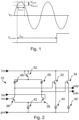
- FIG. 1 illustrates an example of peak detection in an RF signal (V RF ) according to an embodiment of this disclosure.
- V RF RF signal
- the RF signal is assumed to be a simple sine wave, although it will be appreciated that embodiments of this disclosure would be applicable to RF signals having other waveforms.
- Embodiments of this disclosure may allow for swift detection and assertion of the control signal V control , once V RF crosses V detect . This goal may be complicated by the fact that V RF may only spend a short time above V detect (that is to say, t detect may be small).
- V peak ⁇ V detect V peak ⁇ V detect
- V control may be transitioned/asserted within the time t act , such that appropriate action can be taken in response to the detected signal V RF crossing V detect for protecting the driven circuitry.
- t act may include multiple signal periods of V RF . In accordance with embodiments of this disclosure, it has been realized that this fact may be used to the advantage of a protection circuit or method for protecting the driven circuitry.
- V detect is a positive voltage and peaks are detected when V RF > V detect
- embodiments of this disclosure may also be applied negative peaks in V RF (i.e. V detect is a negative voltage and peaks are detected when V RF ⁇ V detect ).
- a protection circuit may be operable to detect both positive and negative peaks in V RF .
- the terms “exceed” and “exceeds” refer to V RF exceeding a detection level V detect in the sense that, for a positive part of the V RF waveform (positive peak), V RF > V detect and/or, for a negative part of the V RF waveform (negative peak), V RF ⁇ V detect .
- Embodiments of this disclosure can provide a protection circuit for protecting driven circuitry against voltage peaks in a radio frequency signal, "V RF ".
- V RF radio frequency signal
- voltage peaks past a predetermined voltage level, "V detect " may be detected and acted upon to protect the driven circuitry.
- the protection circuit may include a number of features including an input, an amplification stage, a hold circuit and a latch circuit.
- the input is configured to receive the radio frequency signal.
- the amplification stage is coupled to the input for receipt of a signal based upon the radio frequency signal received by the input.
- the radio frequency signal may be processed by the protection circuit prior to being fed to the amplification stage.
- the radio frequency signal may be biased for maintaining a linear region of the first amplification stage at a desired common mode level.
- the amplification stage is operable to produce an amplified signal based on V detect -V RF . Further details of the amplification stage will be described below.
- the amplified signal may be then be assessed by the hold circuit, to determine whether a peak voltage V peak of the radio frequency signal exceeds V detect .
- the hold circuit may thus make a determination as to whether the peak voltage of the radio frequency signal is exceeding safe levels for preventing damage to the driven circuitry. Based on this assessment, the hold circuit may then output a detection value, indicative of the assessment. In particular, the hold circuit may output a first detection value if V peak exceeds V detect , or a second detection value if V peak does not exceed V detect .
- the latch circuit may then latch the detection value produced by the hold circuit. This latched value may then be used by the protection circuit to, if necessary, take action to prevent damage to the driven circuitry. This action may, for instance, include enabling/disabling an output stage of the protection circuit and/or attenuating the radio frequency signal.
- Figure 2 shows an example of an amplification stage 10 for a protection circuit according to an embodiment of this disclosure.
- the amplification stage 10 includes a first (e.g. positive) input Inp and a second (e.g. negative) input Inn.
- the first input Inp may be coupled to receive the radio frequency signal from the input of the protection circuit. As will be described below in relation to Figure 5 , the voltage received by the first input Inp may be biased.
- the second input Inn may be coupled to receive a voltage based on the predetermined voltage level V detect .
- the amplification stage 10 also includes a first transistor 38 and a second transistor 36.
- the first input Inp is coupled to a control terminal (e.g. base) of the first transistor 38 and the second input Inn is coupled to a control terminal (e.g. base) of the second transistor 36.
- a first current terminal (e.g. collector) of each of the first and second transistors 38, 36 may be coupled to a second current terminal (e.g. emitter) of a third transistor 52 via a respective resistor 50, 48.
- a control terminal (e.g. base) and a first current terminal (e.g. collector) of the third transistor 52 may be coupled to a supply rail Vcc.
- a second current terminal (e.g. emitter) of each of the first and second transistors 38, 36 may be coupled to a current source 42.
- the current source 42 may be coupled between the second current terminals of the first and second transistors 38, 36 and a reference voltage, e.g. ground.
- the amplification stage 10 further includes a fourth transistor 32 and a firth transistor 34.
- a first current terminal (e.g. collector) of each of the fourth and fifth transistors 32, 34 may be coupled to the supply rail Vcc.
- a second current terminal (e.g. emitter) of each of the fourth and fifth transistors 32, 34 may be coupled to a respective current source 44, 46.
- Each current source 44, 46 may be coupled between the second current terminals of the fourth and fifth transistors 32, 34 and the aforementioned reference voltage (e.g. ground).
- a control terminal (e.g. base) of the fourth transistor 32 may be coupled to a node located between the second transistor 36 and its respective resistor 48.
- a control terminal (e.g. base) of the fifth transistor 34 may be coupled to a node located between the first transistor 38 and its respective resistor 50.
- the amplification stage 10 also includes a first (e.g. positive) output outp and a second (e.g. negative) output outn.
- the first output outp may be coupled to a node located between the second current terminal of the fourth transistor 32 and its respective current source 44.
- the second output outn may be coupled to a node located between the second current terminal of the fifth transistor 34 and its respective current source 46.
- the components of the amplification stage 10 shown in Figure 2 may produce a differential output (based on the difference between outp and outn) which is an amplified output based on the signals received by the inputs Inp and Inn. Since Inp and Inn receive signals based on the radio frequency signal and the predetermined voltage level V detect , respectively, the differential output of the amplification stage 10 is an amplified signal based on V detect - V RF .
- the outputs outp and outn may be coupled to the inputs to a further amplification stage 10 of like configuration to the amplification stage 10 shown in Figure 2 , for further amplification of the amplified signal based on V detect - V RF .
- an number of amplification stages 10 of the kind shown in Figure 2 may be coupled together in a linear chain, to achieve a desired amount of amplification of the amplified signal based on V detect -V RF . It is envisaged that in some embodiments, a single amplification stage 10 may suffice for a given application.
- the outputs outp and outn of a final amplification stage 10 in the linear chain of amplification stages 10 may be coupled to the inputs of a hold circuit of the protection circuit, an embodiment of which will be described below in relation to Figure 3 .
- the transistors 36, 38, 52, 32, 34 in the present embodiment are npn bipolar transistors, but it is envisaged that other transistor types may be used.
- circuit described above in relation to Figure 2 is merely an example of a suitable circuit for implementing an amplification stage 10.
- other circuits may be used to implement the amplification stage 10.
- Such alternative arrangements should be operable to receive the radio frequency signal from the input of the protection circuit and produce an amplified signal based on V detect - V RF which may be outputted to a hold circuit of the protection circuit.
- An amplification stage 10 of the kind shown in Figure 2 may reduce propagation delay within the protection circuit while also increasing the bandwidth offered for processing V RF to detect peaks that exceed V detect .
- the use of a linear chain comprising multiple amplification stages may improve the bandwidth available for the amplification of the amplified signal based on V detect - V RF .
- Figure 3 shows an example of a hold circuit 90 for a protection circuit according to an embodiment of this disclosure.
- the hold circuit 90 includes a first (e.g. positive) input Inp and a second (e.g. negative) input Inn.
- the first input Inp may be coupled to the first output outp of the amplification stage 10 shown in Figure 2 .
- the second input Inn may be coupled to the second output outn of the amplification stage 10 shown in Figure 2 .
- the protection circuit includes a linear chain of multiple amplification stages 10
- the inputs Inp, Inn of the hold circuit 90 may be coupled to the outputs outp, outn of a final amplification stage 10 in the linear chain.
- the hold circuit 90 includes a first transistor 94 and a second transistor 92.
- the first input Inp may be coupled to a control terminal (e.g. base) of the first transistor 94.
- the second input Inn may be coupled to a control terminal (e.g. base) of the second transistor 92.
- a first current terminal (e.g. collector) of the second transistor 92 may be coupled to to a supply rail Vcc.
- a second current terminal (e.g. emitter) of each of the first and second transistors 92, 94 may be coupled to a current source 91.
- the current source 10 may be coupled between the second current terminals of each transistor 92, 94 and a reference voltage, e.g. ground.
- the transistors 92, 94 in the present embodiment are npn bipolar transistors, but it is envisaged that other transistor types may be used.
- the hold circuit 90 also includes an RC network.
- the RC network includes a capacitor 96 and a resistor 98.
- a first terminal of the capacitor 96 and a first terminal of the resistor 98 may be coupled to the supply rail Vcc.
- a second terminal of the capacitor 96 and a second terminal of the resistor 98 may be coupled together at a common node 93.
- a first current terminal (e.g. collector) of the first transistor 94 may be coupled to the common node 93.
- the hold circuit 90 further includes an output RF_ok, which may be coupled to the common node 93.
- the output RF_ok may be coupled to a latch circuit of the protection circuit, an embodiment of which will be described below in relation to Figure 4 .
- the hold circuit 90 determines, from the signal received at the inputs Inp, Inn (which, as explained above, is an amplified signal based on V detect - V RF produced by the amplification stage 10 coupled to the hold circuit) whether a peak voltage V peak of the radio frequency signal exceeds V detect . According to this determination, the output RF_ok outputs a detection value. In particular, the output RF_ok outputs a first (e.g. negative, low) detection value if V peak exceeds V detect , and outputs a second (e.g. positive, high) detection value if V peak does not exceed V detect .
- a first e.g. negative, low
- a second detection value e.g. positive, high
- the hold circuit 90 shown in Figure 3 may react quickly to changes in the determination as to whether a peak voltage V peak of the radio frequency signal exceeds V detect and accordingly quickly alter its outputted detection value. This swift detection and output operation may be afforded by the simplicity of the hold circuit 90.
- the transition between the case in which V RF does not exceed V detect and the case in which V RF does exceed V detect will be described in more detail below.
- V peak of the radio frequency signal V RF will be less than V detect . Accordingly, the amplification stage 10 (or linear chain of amplification stages 10) will continuously have a negative output (i.e. outp ⁇ outn in Figure 2 ). Accordingly, the inputs of the hold circuit 90 will have Inp ⁇ Inn, so predominantly all current of the current source 91 will flow through the second transistor 92, hence the output RF_ok of the hold circuit 90 will remain at the second detection value (high, in this embodiment). Note that at this point, the capacitor 96 is uncharged.
- V RF does cross the V detect level
- the hold circuit 90 will have Inp > Inn for a part of the period of the oscillating radio frequency signal V RF (again, V RF is assumed to be sinusoidal, merely for the purposes of illustration).
- V RF is assumed to be sinusoidal, merely for the purposes of illustration.
- the resistance of the resistor 98 may be chosen to be high enough such that the output RF_ok signal will not drop significantly before the next pulse in V RF arrives. Accordingly, output RF_ok will continue to drop while each pulse in V RF continues to exceed V detect . Subsequently, output RF_ok will reach a value corresponding to the first detection value (low, in this embodiment).
- Appropriate selection of the parameters of the RC network may allow the protection circuit to be tuned according to the desired number of pulses in V RF required (and accordingly the transition time, once the frequency of V RF is considered) for the output RF_ok to transition from the second detection value to the first detection value, when V RF exceeds V detect .
- Figure 4 shows a latch circuit 130 for a protection circuit according to an embodiment of this disclosure.
- the latch circuit 130 has a first input, which is coupled to the output RF_ok of the hold circuit 90 of Figure 3 .
- the latch circuit 90 also includes a first NAND gate 132 and a second NAND gate 134.
- the first and second NAND gates 132, 134 are cross-coupled such that the output of each NAND gate 132, 134 is coupled to one of the inputs of the other NAND gate 134, 132.
- the first input of the latch circuit 130 is coupled to another of the inputs if the first NAND gate 132, to apply RF_ok to the NAND gate 132.
- Another of the inputs of the second NAND gate is coupled to a reset input of the latch circuit via a NOT gate 136. Note that the opposite logic value of the value of RF_ok is latched by the latch circuit 130 into the output of the first NAND gate 132 (i.e. the output of the first NAND gate 132 is high when RF_ok is low, and vice versa).
- the latch circuit 130 may also include features for acting on the latched value of RF_ok.
- the latch circuit 130 may further include a NOR gate 140.
- An input of the NOR gate 140 may be coupled to the output of the first NAND gate 132, to receive the latched value of (the logical opposite value of) RF_ok.
- Another input of the NOR gate 140 may be coupled to an enable input en_in of the latch circuit via a NOT gate 138.
- An output of the NOR gate may be coupled to an enable output en_out of the latch circuit 130. Note that en_out is low unless the output of the first NAND gate 132 (which is the logical opposite value of RF_ok) is low and en_in is high.
- the output en_out may be used to apply a control signal for enabling/disabling an output stage of the protection circuit according to the latched detection value RF_ok. For instance, in this embodiment, when RF_ok is low (indicating that V peak exceeds V detect ), the latched output of the first NAND gate 132 will be high. On the other hand, when RF_ok is high (indicating that V peak does not exceed V detect ), the latched output of the first NAND gate 132 will be low.
- en_in may be used to enable/disable the output stage of the protection circuit even if RF_ok is high (indicating that V peak does not exceed V detect ).
- Another feature of the latch circuit 130 for acting on the latched value of RF_ok may comprise and RFshutdown output.
- the RFshutdown output may be coupled to the output of the first NAND gate 132.
- RF_ok is high (indicating that V peak does not exceed V detect )
- the RFshutdown output is low, providing an enable signal for an output stage of the protection circuit to continue operating.
- RF_ok is low (indicating that V peak exceeds V detect )
- the RFshutdown output is high, providing a disable signal for the output stage of the protection circuit to stop operating.
- the RFshutdown output in this embodiment simply keys of the value of RF_ok and does not include separate enable/disable functionality using an enable input as per the NOR gate 140 implementation noted above.
- the RFshutdown output implementation need not introduce a possible delay associated with the NOT gate 138 and the NOR gate 140 into the operation of the enable/disable signal.
- Both the NOR gate 140 implementation and the RFshutdown output implementation described above provide an enable/disable to an output stage of the protection circuit, to cease operation of the output stage when RF_ok indicates that V peak exceeds V detect .
- the RFshutdown out and/or the output en_out may be coupled to an attenuator for attenuating the radio frequency signal.
- the attenuator may attenuate V RF when the output of the NOR gate 140 is low and/or when the value of RFshutdown is high as described above. In this way, an output stage of the protection circuit need not be disabled when V peak exceeds V detect , but V RF may be simply attenuated to avoid damage to the driven circuitry.
- the attenuator may be programmable, so as to allow the attenuation level to be set according to the protection requirements of the driven circuitry.
- Figure 5 shows a protection circuit 100 according to an embodiment of this disclosure.
- the protection circuit 100 includes an input RFin for receiving the radio frequency signal, V RF .
- a low noise amplifier 102 is provided for amplifying V RF .
- the low noise amplifier 102 may be considered to be part of the protection circuit 100, but in other embodiments the low noise amplifier 102 may be considered to be separate from the protection circuit 100.
- the protection circuit 100 also includes a linear chain of amplification stages 104, 106, 108, 110, 112.
- Each amplification stage may be an amplification stage 10 of the kind described above in relation to Figure 2 .
- each amplification stage 104, 106, 108, 110, 122 may include two inputs and two outputs. As described previously, the inputs of the intermediate stages 106, 108, 110 in the linear chain may be coupled to the outputs of a preceding amplification stage in the linear chain.
- a first input (e.g. Inp in Figure 2 ) of the first amplification stage 104 in the linear chain may be coupled to the input RFin to receive V RF .
- the first input of the first amplification stage 104 is coupled to the output of the low noise amplifier 102, whereby the first input of the first amplification stage 104 is coupled to the input RFin via the low noise amplifier 102.
- a high pass filter capacitor 103 may also be coupled between the output of the low noise amplifier 102 and the first input of the first amplification stage 104.
- the first input of the first amplification stage 104 may be biased by a voltage Vbias.
- the bias voltage Vbias may be chosen to maintain a linear region of the first amplification stage at a desired common mode level.
- the bias voltage V bias may be programmable, dependent upon the characteristics of the first amplification stage 104 and V RF .
- a second input (e.g. Inn in Figure 2 ) of the first amplification stage 104 may be coupled to receive a signal (voltage) based of V detect .
- a low pass filter capacitor 122 may be used to filter the voltage applied at the second input of the first amplification stage 104.
- Resistor 121 may be used to offset the value of V detect .
- the value of V detect is set relative to the value of V bias . Note that V detect may also be programmable.
- the outputs of the first amplification stage 104 are coupled to a next amplification stage 106 in the linear chain.
- the hold circuit 90 may be a hold circuit of the kind described above in relation to Figure 3 .
- the protection circuit 100 further includes a latch circuit 130.
- the latch circuit 130 may be a latch circuit 130 of the kind described above in relation to Figure 4 .
- an output RF_ok of the hold circuit 90 may be coupled to an input of the latch circuit 130, to allow the detection value outputted by the hold circuit 90 to be latched and acted upon.
- the hold circuit 130 in this embodiment includes a reset input, an enable input en_in and an enable output en_out.
- the enable output may be coupled to the low noise amplifier 102, for instance to control the low noise amplifier 102 (or an attenuator located in the signal path with the low noise amplifier 102) to attenuate the radio frequency signal V RF in the event that V peak exceeds V detect .
- the latch circuit 130 may additionally (or alternatively) include an RFshutdown output.
- the protection circuit may be operable to protect driven circuitry against voltage peaks in a radio frequency signal, "V RF ", past a plurality of different predetermined voltage levels "V detect ". In this way, multiple different protection voltage levels may be provided (e.g. corresponding to increasing values of V detect ).
- the protection circuit may include a plurality of respective sets of one or more amplification stages coupled to the input.
- Each set may include a single amplification stage as described above, or a plurality of amplification stages arranged in a linear chain as described in relation to Figure 5 .
- Each set of amplification stages may thus produce an amplified signal based on V detect - V RF as described above, for each different respective predetermined voltage level.
- the protection circuit may also include a plurality of respective hold circuits.
- the input of each hold circuit may be coupled to the output of a respective one of the sets of one or more amplification stages as described above.
- Each hold circuit may therefore determine, from the amplified signal produced a respective one of the sets of one or more amplification stages, whether a peak voltage V peak of the radio frequency signal exceeds the respective predetermined voltage level for that set.
- Each hold circuit can then output a first detection value if V peak exceeds V detect for that set of one or more amplification stages, and a second detection value if V peak does not exceed V detect for that set of one or more amplification stages.
- the protection circuit may further include a plurality of respective latch circuits, each operable to latch the detection value outputted by a respective one of the hold circuits.
- each parallel arrangement may further include any of the additional details described above in relation to the "single V detect " arrangement shown in Figure 5 .
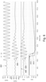
- Figure 6 illustrates the operation of a protection circuit according to an embodiment of this disclosure.
- the following plots are shown:
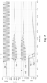
- Figure 7 illustrates the operation of a protection circuit according to an embodiment of this disclosure.
- the following plots are shown:
- Plots 602, 702 in Figures 6 and 7 each show RFin increasing (abruptly, in this example) from a relatively low amplitude to an amplitude which triggers the protection circuit 100.
- Plots 604, 704 in Figures 6 and 7 each show the signal seen by the circuit to be protected (i.e. the output of the low noise amplifier 102 is provided to the circuit to be protected in this embodiment (this connection is not shown in Figure 5 )).
- Plots 606, 706 and 608, 708 in Figures 6 and 7 each show how the output (RF_out) of the low noise amplifier 102 exceeds V detect , following the increase in amplitude of RFin.
- Plots 610 and 710 in Figures 6 and 7 each illustrate that embodiments of this disclosure can pull down RF_ok quickly, in reaction to RF_out exceeding V detect .
- the reaction time of the protection circuit 100 i.e. from RF_out exceeding V detect
- the reaction time of the protection circuit 100 is very fast (around 0.6ns).
- the protection circuit includes an input for receiving the radio frequency signal.
- the protection circuit also includes at least one amplification stage coupled to the input.
- the amplification stage is operable to produce an amplified signal based on V detect - V RF .
- the protection circuit further includes a hold circuit operable to determine, from the amplified signal produced by the amplification stage, whether a peak voltage V peak of the radio frequency signal exceeds V detect .
- the hold circuit is operable to output a first detection value if V peak exceeds V detect .
- the hold circuit is operable to output a second detection value if V peak does not exceed V detect .
- the protection circuit also includes a latch circuit operable to latch the detection value outputted by the hold circuit.
Landscapes
- Engineering & Computer Science (AREA)
- Power Engineering (AREA)
- Microelectronics & Electronic Packaging (AREA)
- Physics & Mathematics (AREA)
- General Physics & Mathematics (AREA)
- Amplifiers (AREA)
Claims (12)
- Schutzschaltung (100) zum Schützen angesteuerter Schaltkreise vor Spannungsspitzen in einem Hochfrequenzsignal "VRF" über einem vorbestimmten Spannungspegel "Vdetect", wobei die Schutzschaltung Folgendes umfasst:einen Eingang zum Empfangen des Hochfrequenzsignals;eine Vielzahl N von Verstärkungsstufen (10, 104, 106, 108, 110, 112), die in einer linearen Kette angeordnet sind, um eine Bandbreite zu verbessern, die zur Erzeugung eines verstärkten Signals verfügbar ist, auf der Basis von Vdetect - VRF, wobei die Vielzahl von Verstärkungsstufen Folgendes umfasst:eine erste Verstärkungsstufe (104), die mit dem Eingang gekoppelt ist;eine N-te Verstärkungsstufe (112) mit einem Ausgang, der betreibbar ist zum Ausgeben des verstärkten Signals auf der Basis von Vdetect - VRF; undmindestens eine Zwischenverstärkungsstufe (106, 108, 110), die zwischen die erste Verstärkungsstufe und die N-te Verstärkungsstufe in der linearen Kette geschaltet ist;eine Halteschaltung (90), die betreibbar ist, um aus dem durch die mindestens eine Verstärkungsstufe erzeugten verstärkten Signal zu bestimmen, ob eine Spitzenspannung Vpeak des Hochfrequenzsignals Vdetect überschreitet, und um Folgendes auszugeben:einen ersten Detektionswert, wenn Vpeak Vdetect überschreitet; undeinen zweiten Detektionswert, wenn Vpeak Vdetect nicht überschreitet; undeine Latch-Schaltung (130), betreibbar zum Latchen des durch die Halteschaltung ausgegebenen Detektionswerts, wobeidie Latch-Schaltung einen Ausgang umfasst, der betreibbar ist zum Ausgeben eines Steuersignals zum Freigeben/Sperren einer Ausgangsstufe der Schutzschaltung gemäß dem gelatchten Detektionswert; oderdie Schutzschaltung ferner ein programmierbares Dämpfungsglied zum Dämpfen des Hochfrequenzsignals gemäß dem gelatchten Detektionswert.
- Schutzschaltung nach Anspruch 1, wobei jede Verstärkungsstufe der N Verstärkungsstufen eine Differenzverstärkungsstufe ist, die ein Paar von Eingängen und ein Paar von Ausgängen umfasst.
- Schutzschaltung nach Anspruch 2, wobei das Paar von Eingängen der ersten Verstärkungsstufe Folgendes umfasst:einen ersten Eingang, der mit dem Eingang der Schutzschaltung gekoppelt ist, undeinen zweiten Eingang, der mit einer Referenzspannung gekoppelt ist, die durch Vdetect bestimmt wird.
- Schutzschaltung nach Anspruch 3, wobei der erste Eingang programmierbar vorspannbar ist, um eine lineare Region der ersten Verstärkungsstufe auf einem gewünschten Gleichtaktpegel zu halten.
- Schutzschaltung nach Anspruch 3 oder Anspruch 4, wobei die Referenzspannung programmierbar ist.
- Schutzschaltung nach einem der Ansprüche 2 bis 5, wobei das Paar von Eingängen jeder Zwischenverstärkungsstufe mit dem Paar von Ausgängen einer vorhergehenden Verstärkungsstufe in der linearen Kette gekoppelt ist.
- Schutzschaltung nach einem der Ansprüche 2 bis 6, wobei die Halteschaltung einen Differenzeingang aufweist und wobei das Paar von Ausgängen der N-ten Verstärkungsstufe mit dem Differenzeingang der Halteschaltung gekoppelt ist.
- Schutzschaltung nach einem der vorhergehenden Ansprüche, wobei ein rauscharmer Verstärker (102) geschaltet ist zum Empfangen des Hochfrequenzsignals und wobei die erste Verstärkungsstufe mit einem Ausgang des rauscharmen Verstärkers gekoppelt ist.
- Schutzschaltung nach einem der vorhergehenden Ansprüche, wobei die erste Halteschaltung Folgendes umfasst:einen Ausgang zum Ausgeben des Detektionswerts an die Latch-Schaltung undein RC-Netzwerk (96, 98) zum Einstellen einer Übergangszeit der Halteschaltung zwischen dem zweiten Detektionswert und dem ersten Detektionswert.
- Schutzschaltung nach Anspruch 9, wobei das RC-Netzwerk einen Kondensator (96) umfasst, der auf der Basis des durch die Verstärkungsstufe ausgegebenen verstärkten Signals betreibbar ist zum Ungeladenbleiben, während Vpeak Vdetect; und nicht überschreitet; und
Laden, wenn Vpeak Vdetect überschreitet, zum Ansteuern des durch die Halteschaltung ausgegebenen Detektionswerts auf den zweiten Detektionswert über einen Zeitraum, der durch eine Zeitkonstante des RC-Netzwerks bestimmt wird. - Schutzschaltung nach einem der vorhergehenden Ansprüche, wobei die Schutzschaltung betreibbar ist zum Schützen von angesteuerten Schaltkreisen vor Spannungsspitzen in einem Hochfrequenzsignal "VRF" über einer Vielzahl von verschiedenen vorbestimmten Spannungspegeln "Vdetect", wobei die Schutzschaltung Folgendes umfasst:den Eingang zum Empfangen des Hochfrequenzsignals;mehrere jeweilige Mengen der Vielzahl N von Verstärkungsstufen, die mit dem Eingang gekoppelt sind,wobei jede Menge zum Erzeugen eines verstärkten Signals auf der Basis von Vdetect - VRF für jeden verschiedenen jeweiligen vorbestimmten Spannungspegel dient;eine Vielzahl von jeweiligen Halteschaltungen, jeweils betreibbar zum Bestimmen aus dem durch eine jeweilige der Mengen einer oder mehrerer Verstärkungsstufen erzeugten verstärkten Signal, ob eine Spitzenspannung Vpeak des Hochfrequenzsignals den jeweiligen vorbestimmten Spannungspegel für diese Menge überschreitet, und zum Ausgeben voneinem ersten Detektionswert, wenn Vpeak Vdetect für diese Menge einer oder mehrerer Verstärkungsstufen überschreitet; undeinem zweiten Detektionswert, wenn Vpeak Vdetect für diese Menge einer oder mehrerer Verstärkungsstufen nicht überschreitet; undeine Vielzahl von jeweiligen Latch-Schaltungen, jeweils betreibbar zum Latchen des durch eine jeweilige der Halteschaltungen ausgegebenen Detektionswerts.
- Verfahren zum Schützen von angesteuerten Schaltkreisen vor Spannungsspitzen in einem Hochfrequenzsignal "VRF" über einem vorbestimmten Spannungspegel "Vdetect", wobei das Verfahren Folgendes umfasst:einen Eingang zum Empfangen des Hochfrequenzsignals;eine Vielzahl N von Verstärkungsstufen (10, 104, 106, 108, 110, 112), die auf der Basis von Vdetect - VRF ein verstärktes Signal erzeugen, wobei die Vielzahl N von Verstärkungsstufen in einer linearen Kette angeordnet sind, um eine Bandbreite zu verbessern, die zur Erzeugung des verstärkten Signals verfügbar ist, auf der Basis von Vdetect - VRF, wobei die Vielzahl von Verstärkungsstufen Folgendes umfasst:eine erste Verstärkungsstufe (104), die mit dem Eingang gekoppelt ist;eine N-te Verstärkungsstufe (112) mit einem Ausgang, der betreibbar ist zum Ausgeben des verstärkten Signals auf der Basis von Vdetect - VRF; undmindestens eine Zwischenverstärkungsstufe (106, 108, 110), die zwischen die erste Verstärkungsstufe und die N-te Verstärkungsstufe in der linearen Kette geschaltet ist;Bestimmen aus dem verstärkten Signal, ob eine Spitzenspannung Vpeak des Hochfrequenzsignals Vdetect überschreitet;Latchen:einen ersten Detektionswert, wenn Vpeak Vdetect überschreitet; undeines zweiten Detektionswerts, wenn Vpeak Vdetect nicht überschreitet; und entwederAusgeben eines Steuersignals zum Freigeben/Sperren einer Ausgangsstufe gemäß dem gelatchten Detektionswert; oderDämpfen des Hochfrequenzsignals gemäß dem gelatchten Detektionswert.
Priority Applications (3)
| Application Number | Priority Date | Filing Date | Title |
|---|---|---|---|
| EP21167721.6A EP4072011B1 (de) | 2021-04-09 | 2021-04-09 | Schutzschaltung und verfahren |
| CN202210151064.6A CN115208332A (zh) | 2021-04-09 | 2022-02-14 | 保护电路和方法 |
| US17/658,010 US12323111B2 (en) | 2021-04-09 | 2022-04-05 | Protection circuit and method |
Applications Claiming Priority (1)
| Application Number | Priority Date | Filing Date | Title |
|---|---|---|---|
| EP21167721.6A EP4072011B1 (de) | 2021-04-09 | 2021-04-09 | Schutzschaltung und verfahren |
Publications (2)
| Publication Number | Publication Date |
|---|---|
| EP4072011A1 EP4072011A1 (de) | 2022-10-12 |
| EP4072011B1 true EP4072011B1 (de) | 2025-06-25 |
Family
ID=75441844
Family Applications (1)
| Application Number | Title | Priority Date | Filing Date |
|---|---|---|---|
| EP21167721.6A Active EP4072011B1 (de) | 2021-04-09 | 2021-04-09 | Schutzschaltung und verfahren |
Country Status (3)
| Country | Link |
|---|---|
| US (1) | US12323111B2 (de) |
| EP (1) | EP4072011B1 (de) |
| CN (1) | CN115208332A (de) |
Family Cites Families (7)
| Publication number | Priority date | Publication date | Assignee | Title |
|---|---|---|---|---|
| US4654587A (en) | 1985-08-30 | 1987-03-31 | Rockwell International Corporation | Digital peak detector and method of peak detection |
| US9559639B2 (en) * | 2009-08-19 | 2017-01-31 | Qualcomm Incorporated | Protection circuit for power amplifier |
| US20120034895A1 (en) * | 2010-08-03 | 2012-02-09 | Quintic Holdings | Circuit and Method for Peak Detection with Hysteresis |
| US8854130B2 (en) * | 2012-06-25 | 2014-10-07 | Silicon Laboratories Inc. | DC-coupled peak detector |
| US9088257B2 (en) * | 2013-03-15 | 2015-07-21 | Avago Technologies General Ip (Singapore) Pte. Ltd. | Device and method for controlling power amplifier |
| US9379675B2 (en) * | 2014-02-20 | 2016-06-28 | Analog Devices Global | Power detector with overdrive detection |
| US9939467B1 (en) | 2016-10-14 | 2018-04-10 | Analog Devices, Inc. | Wide-range precision RF peak detector |
-
2021
- 2021-04-09 EP EP21167721.6A patent/EP4072011B1/de active Active
-
2022
- 2022-02-14 CN CN202210151064.6A patent/CN115208332A/zh active Pending
- 2022-04-05 US US17/658,010 patent/US12323111B2/en active Active
Also Published As
| Publication number | Publication date |
|---|---|
| CN115208332A (zh) | 2022-10-18 |
| EP4072011A1 (de) | 2022-10-12 |
| US12323111B2 (en) | 2025-06-03 |
| US20220329214A1 (en) | 2022-10-13 |
Similar Documents
| Publication | Publication Date | Title |
|---|---|---|
| JP4390706B2 (ja) | フェイルセーフ差動増幅器回路 | |
| US5703530A (en) | Radio frequency amplifier having improved CTB and cross modulation characteristics | |
| CN100578919C (zh) | 放大器单元及其故障检测方法 | |
| CN104965117A (zh) | 高线性快速峰值检测器 | |
| US20020153958A1 (en) | Signal amplifier and optical signal receiver using the same | |
| KR20110090751A (ko) | 검출회로와 그것을 사용한 반도체장치 | |
| US9843295B2 (en) | Transimpedance amplifier | |
| KR20190049096A (ko) | 차량용 레이다 시스템 | |
| CN102369663A (zh) | 宽带干扰检测器 | |
| US8476972B2 (en) | Method and apparatus for amplifying a time difference | |
| US20020187766A1 (en) | Circuit for compensating temperature of automatic gain control circuit | |
| EP4072011B1 (de) | Schutzschaltung und verfahren | |
| US20120098597A1 (en) | switch for use in a programmable gain amplifier | |
| EP2106022A1 (de) | Verstärkungsvorrichtung und Verfahren zur Erkennung einer Verstärkerfehlfunktion | |
| US7661879B2 (en) | Apparatus for detecting temperature using transistors | |
| CN106100600B (zh) | 一种微波连续波大功率限幅器 | |
| US7429891B2 (en) | Method and system for low noise amplifier (LNA) gain adjustment through narrowband received signal strength indicator (NRSSI) | |
| US20040251969A1 (en) | Method and apparatus for detecting interruption of an input signal with cancellation of offset level | |
| US10432319B2 (en) | Receivers with automatic gain control | |
| US10236851B2 (en) | Wide bandwidth variable gain amplifier and exponential function generator | |
| US20150381120A1 (en) | Slew rate control boost circuits and methods | |
| EP3675358B1 (de) | Hochgeschwindigkeitsentscheidungsvorrichtung | |
| US20110068862A1 (en) | Feedback amplifier and feedback amplification method | |
| DE102006012967A1 (de) | Aktiver Begrenzer mit integriertem Sensor | |
| US20200036351A1 (en) | Signal level detection and overrange signal limiter and clamp for electronic circuits |
Legal Events
| Date | Code | Title | Description |
|---|---|---|---|
| PUAI | Public reference made under article 153(3) epc to a published international application that has entered the european phase |
Free format text: ORIGINAL CODE: 0009012 |
|
| STAA | Information on the status of an ep patent application or granted ep patent |
Free format text: STATUS: THE APPLICATION HAS BEEN PUBLISHED |
|
| AK | Designated contracting states |
Kind code of ref document: A1 Designated state(s): AL AT BE BG CH CY CZ DE DK EE ES FI FR GB GR HR HU IE IS IT LI LT LU LV MC MK MT NL NO PL PT RO RS SE SI SK SM TR |
|
| STAA | Information on the status of an ep patent application or granted ep patent |
Free format text: STATUS: REQUEST FOR EXAMINATION WAS MADE |
|
| 17P | Request for examination filed |
Effective date: 20230412 |
|
| RBV | Designated contracting states (corrected) |
Designated state(s): AL AT BE BG CH CY CZ DE DK EE ES FI FR GB GR HR HU IE IS IT LI LT LU LV MC MK MT NL NO PL PT RO RS SE SI SK SM TR |
|
| GRAP | Despatch of communication of intention to grant a patent |
Free format text: ORIGINAL CODE: EPIDOSNIGR1 |
|
| STAA | Information on the status of an ep patent application or granted ep patent |
Free format text: STATUS: GRANT OF PATENT IS INTENDED |
|
| RIC1 | Information provided on ipc code assigned before grant |
Ipc: G01R 19/04 20060101ALN20250131BHEP Ipc: G01R 19/165 20060101ALI20250131BHEP Ipc: H03F 3/45 20060101ALI20250131BHEP Ipc: H03F 3/19 20060101ALI20250131BHEP Ipc: H03F 1/52 20060101AFI20250131BHEP |
|
| INTG | Intention to grant announced |
Effective date: 20250221 |
|
| GRAS | Grant fee paid |
Free format text: ORIGINAL CODE: EPIDOSNIGR3 |
|
| GRAA | (expected) grant |
Free format text: ORIGINAL CODE: 0009210 |
|
| STAA | Information on the status of an ep patent application or granted ep patent |
Free format text: STATUS: THE PATENT HAS BEEN GRANTED |
|
| AK | Designated contracting states |
Kind code of ref document: B1 Designated state(s): AL AT BE BG CH CY CZ DE DK EE ES FI FR GB GR HR HU IE IS IT LI LT LU LV MC MK MT NL NO PL PT RO RS SE SI SK SM TR |
|
| REG | Reference to a national code |
Ref country code: GB Ref legal event code: FG4D |
|
| REG | Reference to a national code |
Ref country code: CH Ref legal event code: EP |
|
| REG | Reference to a national code |
Ref country code: CH Ref legal event code: EP |
|
| REG | Reference to a national code |
Ref country code: IE Ref legal event code: FG4D |
|
| REG | Reference to a national code |
Ref country code: DE Ref legal event code: R096 Ref document number: 602021032686 Country of ref document: DE |
|
| PG25 | Lapsed in a contracting state [announced via postgrant information from national office to epo] |
Ref country code: FI Free format text: LAPSE BECAUSE OF FAILURE TO SUBMIT A TRANSLATION OF THE DESCRIPTION OR TO PAY THE FEE WITHIN THE PRESCRIBED TIME-LIMIT Effective date: 20250625 |
|
| REG | Reference to a national code |
Ref country code: LT Ref legal event code: MG9D |
|
| PG25 | Lapsed in a contracting state [announced via postgrant information from national office to epo] |
Ref country code: NO Free format text: LAPSE BECAUSE OF FAILURE TO SUBMIT A TRANSLATION OF THE DESCRIPTION OR TO PAY THE FEE WITHIN THE PRESCRIBED TIME-LIMIT Effective date: 20250925 Ref country code: GR Free format text: LAPSE BECAUSE OF FAILURE TO SUBMIT A TRANSLATION OF THE DESCRIPTION OR TO PAY THE FEE WITHIN THE PRESCRIBED TIME-LIMIT Effective date: 20250926 |
|
| PG25 | Lapsed in a contracting state [announced via postgrant information from national office to epo] |
Ref country code: BG Free format text: LAPSE BECAUSE OF FAILURE TO SUBMIT A TRANSLATION OF THE DESCRIPTION OR TO PAY THE FEE WITHIN THE PRESCRIBED TIME-LIMIT Effective date: 20250625 |
|
| PG25 | Lapsed in a contracting state [announced via postgrant information from national office to epo] |
Ref country code: HR Free format text: LAPSE BECAUSE OF FAILURE TO SUBMIT A TRANSLATION OF THE DESCRIPTION OR TO PAY THE FEE WITHIN THE PRESCRIBED TIME-LIMIT Effective date: 20250625 |
|
| PG25 | Lapsed in a contracting state [announced via postgrant information from national office to epo] |
Ref country code: RS Free format text: LAPSE BECAUSE OF FAILURE TO SUBMIT A TRANSLATION OF THE DESCRIPTION OR TO PAY THE FEE WITHIN THE PRESCRIBED TIME-LIMIT Effective date: 20250925 |
|
| PG25 | Lapsed in a contracting state [announced via postgrant information from national office to epo] |
Ref country code: LV Free format text: LAPSE BECAUSE OF FAILURE TO SUBMIT A TRANSLATION OF THE DESCRIPTION OR TO PAY THE FEE WITHIN THE PRESCRIBED TIME-LIMIT Effective date: 20250625 |
|
| REG | Reference to a national code |
Ref country code: NL Ref legal event code: MP Effective date: 20250625 |
|
| PG25 | Lapsed in a contracting state [announced via postgrant information from national office to epo] |
Ref country code: NL Free format text: LAPSE BECAUSE OF FAILURE TO SUBMIT A TRANSLATION OF THE DESCRIPTION OR TO PAY THE FEE WITHIN THE PRESCRIBED TIME-LIMIT Effective date: 20250625 |
|
| PG25 | Lapsed in a contracting state [announced via postgrant information from national office to epo] |
Ref country code: PT Free format text: LAPSE BECAUSE OF FAILURE TO SUBMIT A TRANSLATION OF THE DESCRIPTION OR TO PAY THE FEE WITHIN THE PRESCRIBED TIME-LIMIT Effective date: 20251027 |
|
| REG | Reference to a national code |
Ref country code: AT Ref legal event code: MK05 Ref document number: 1807660 Country of ref document: AT Kind code of ref document: T Effective date: 20250625 |
|
| PG25 | Lapsed in a contracting state [announced via postgrant information from national office to epo] |
Ref country code: IS Free format text: LAPSE BECAUSE OF FAILURE TO SUBMIT A TRANSLATION OF THE DESCRIPTION OR TO PAY THE FEE WITHIN THE PRESCRIBED TIME-LIMIT Effective date: 20251025 |
|
| PG25 | Lapsed in a contracting state [announced via postgrant information from national office to epo] |
Ref country code: AT Free format text: LAPSE BECAUSE OF FAILURE TO SUBMIT A TRANSLATION OF THE DESCRIPTION OR TO PAY THE FEE WITHIN THE PRESCRIBED TIME-LIMIT Effective date: 20250625 Ref country code: SM Free format text: LAPSE BECAUSE OF FAILURE TO SUBMIT A TRANSLATION OF THE DESCRIPTION OR TO PAY THE FEE WITHIN THE PRESCRIBED TIME-LIMIT Effective date: 20250625 |
|
| PG25 | Lapsed in a contracting state [announced via postgrant information from national office to epo] |
Ref country code: CZ Free format text: LAPSE BECAUSE OF FAILURE TO SUBMIT A TRANSLATION OF THE DESCRIPTION OR TO PAY THE FEE WITHIN THE PRESCRIBED TIME-LIMIT Effective date: 20250625 |
|
| PG25 | Lapsed in a contracting state [announced via postgrant information from national office to epo] |
Ref country code: PL Free format text: LAPSE BECAUSE OF FAILURE TO SUBMIT A TRANSLATION OF THE DESCRIPTION OR TO PAY THE FEE WITHIN THE PRESCRIBED TIME-LIMIT Effective date: 20250625 |
|
| PG25 | Lapsed in a contracting state [announced via postgrant information from national office to epo] |
Ref country code: EE Free format text: LAPSE BECAUSE OF FAILURE TO SUBMIT A TRANSLATION OF THE DESCRIPTION OR TO PAY THE FEE WITHIN THE PRESCRIBED TIME-LIMIT Effective date: 20250625 |
|
| PG25 | Lapsed in a contracting state [announced via postgrant information from national office to epo] |
Ref country code: SK Free format text: LAPSE BECAUSE OF FAILURE TO SUBMIT A TRANSLATION OF THE DESCRIPTION OR TO PAY THE FEE WITHIN THE PRESCRIBED TIME-LIMIT Effective date: 20250625 |
|
| PG25 | Lapsed in a contracting state [announced via postgrant information from national office to epo] |
Ref country code: ES Free format text: LAPSE BECAUSE OF FAILURE TO SUBMIT A TRANSLATION OF THE DESCRIPTION OR TO PAY THE FEE WITHIN THE PRESCRIBED TIME-LIMIT Effective date: 20250625 |